EP3093884A1 - Electronic apparatus - Google Patents
Electronic apparatus Download PDFInfo
- Publication number
- EP3093884A1 EP3093884A1 EP15765100.1A EP15765100A EP3093884A1 EP 3093884 A1 EP3093884 A1 EP 3093884A1 EP 15765100 A EP15765100 A EP 15765100A EP 3093884 A1 EP3093884 A1 EP 3093884A1
- Authority
- EP
- European Patent Office
- Prior art keywords
- integrated circuit
- semiconductor integrated
- radiation
- cooling device
- cooling
- Prior art date
- Legal status (The legal status is an assumption and is not a legal conclusion. Google has not performed a legal analysis and makes no representation as to the accuracy of the status listed.)
- Granted
Links
Images
Classifications
-
- H—ELECTRICITY
- H10—SEMICONDUCTOR DEVICES; ELECTRIC SOLID-STATE DEVICES NOT OTHERWISE PROVIDED FOR
- H10W—GENERIC PACKAGES, INTERCONNECTIONS, CONNECTORS OR OTHER CONSTRUCTIONAL DETAILS OF DEVICES COVERED BY CLASS H10
- H10W40/00—Arrangements for thermal protection or thermal control
- H10W40/20—Arrangements for cooling
- H10W40/22—Arrangements for cooling characterised by their shape, e.g. having conical or cylindrical projections
-
- B—PERFORMING OPERATIONS; TRANSPORTING
- B64—AIRCRAFT; AVIATION; COSMONAUTICS
- B64G—COSMONAUTICS; VEHICLES OR EQUIPMENT THEREFOR
- B64G1/00—Cosmonautic vehicles
- B64G1/10—Artificial satellites; Systems of such satellites; Interplanetary vehicles
-
- B—PERFORMING OPERATIONS; TRANSPORTING
- B64—AIRCRAFT; AVIATION; COSMONAUTICS
- B64G—COSMONAUTICS; VEHICLES OR EQUIPMENT THEREFOR
- B64G1/00—Cosmonautic vehicles
- B64G1/22—Parts of, or equipment specially adapted for fitting in or to, cosmonautic vehicles
- B64G1/46—Arrangements or adaptations of devices for control of environment or living conditions
- B64G1/50—Arrangements or adaptations of devices for control of environment or living conditions for temperature control
-
- B—PERFORMING OPERATIONS; TRANSPORTING
- B64—AIRCRAFT; AVIATION; COSMONAUTICS
- B64G—COSMONAUTICS; VEHICLES OR EQUIPMENT THEREFOR
- B64G1/00—Cosmonautic vehicles
- B64G1/22—Parts of, or equipment specially adapted for fitting in or to, cosmonautic vehicles
- B64G1/46—Arrangements or adaptations of devices for control of environment or living conditions
- B64G1/50—Arrangements or adaptations of devices for control of environment or living conditions for temperature control
- B64G1/503—Radiator panels
-
- B—PERFORMING OPERATIONS; TRANSPORTING
- B64—AIRCRAFT; AVIATION; COSMONAUTICS
- B64G—COSMONAUTICS; VEHICLES OR EQUIPMENT THEREFOR
- B64G1/00—Cosmonautic vehicles
- B64G1/22—Parts of, or equipment specially adapted for fitting in or to, cosmonautic vehicles
- B64G1/52—Protection, safety or emergency devices; Survival aids
- B64G1/54—Protection against radiation
-
- B—PERFORMING OPERATIONS; TRANSPORTING
- B64—AIRCRAFT; AVIATION; COSMONAUTICS
- B64G—COSMONAUTICS; VEHICLES OR EQUIPMENT THEREFOR
- B64G1/00—Cosmonautic vehicles
- B64G1/22—Parts of, or equipment specially adapted for fitting in or to, cosmonautic vehicles
- B64G1/52—Protection, safety or emergency devices; Survival aids
- B64G1/54—Protection against radiation
- B64G1/546—Protection against radiation shielding electronic equipment
-
- B—PERFORMING OPERATIONS; TRANSPORTING
- B64—AIRCRAFT; AVIATION; COSMONAUTICS
- B64G—COSMONAUTICS; VEHICLES OR EQUIPMENT THEREFOR
- B64G1/00—Cosmonautic vehicles
- B64G1/22—Parts of, or equipment specially adapted for fitting in or to, cosmonautic vehicles
- B64G1/52—Protection, safety or emergency devices; Survival aids
- B64G1/58—Thermal protection, e.g. heat shields
-
- B—PERFORMING OPERATIONS; TRANSPORTING
- B64—AIRCRAFT; AVIATION; COSMONAUTICS
- B64G—COSMONAUTICS; VEHICLES OR EQUIPMENT THEREFOR
- B64G1/00—Cosmonautic vehicles
- B64G1/22—Parts of, or equipment specially adapted for fitting in or to, cosmonautic vehicles
- B64G1/66—Arrangements or adaptations of apparatus or instruments, not otherwise provided for
-
- G—PHYSICS
- G01—MEASURING; TESTING
- G01J—MEASUREMENT OF INTENSITY, VELOCITY, SPECTRAL CONTENT, POLARISATION, PHASE OR PULSE CHARACTERISTICS OF INFRARED, VISIBLE OR ULTRAVIOLET LIGHT; COLORIMETRY; RADIATION PYROMETRY
- G01J5/00—Radiation pyrometry, e.g. infrared or optical thermometry
- G01J5/0003—Radiation pyrometry, e.g. infrared or optical thermometry for sensing the radiant heat transfer of samples, e.g. emittance meter
- G01J5/0007—Radiation pyrometry, e.g. infrared or optical thermometry for sensing the radiant heat transfer of samples, e.g. emittance meter of wafers or semiconductor substrates, e.g. using Rapid Thermal Processing
-
- G—PHYSICS
- G01—MEASURING; TESTING
- G01T—MEASUREMENT OF NUCLEAR OR X-RADIATION
- G01T1/00—Measuring X-radiation, gamma radiation, corpuscular radiation, or cosmic radiation
- G01T1/16—Measuring radiation intensity
- G01T1/24—Measuring radiation intensity with semiconductor detectors
- G01T1/244—Auxiliary details, e.g. casings, cooling, damping or insulation against damage by, e.g. heat, pressure or the like
-
- H—ELECTRICITY
- H10—SEMICONDUCTOR DEVICES; ELECTRIC SOLID-STATE DEVICES NOT OTHERWISE PROVIDED FOR
- H10D—INORGANIC ELECTRIC SEMICONDUCTOR DEVICES
- H10D84/00—Integrated devices formed in or on semiconductor substrates that comprise only semiconducting layers, e.g. on Si wafers or on GaAs-on-Si wafers
- H10D84/80—Integrated devices formed in or on semiconductor substrates that comprise only semiconducting layers, e.g. on Si wafers or on GaAs-on-Si wafers characterised by the integration of at least one component covered by groups H10D12/00 or H10D30/00, e.g. integration of IGFETs
- H10D84/82—Integrated devices formed in or on semiconductor substrates that comprise only semiconducting layers, e.g. on Si wafers or on GaAs-on-Si wafers characterised by the integration of at least one component covered by groups H10D12/00 or H10D30/00, e.g. integration of IGFETs of only field-effect components
- H10D84/83—Integrated devices formed in or on semiconductor substrates that comprise only semiconducting layers, e.g. on Si wafers or on GaAs-on-Si wafers characterised by the integration of at least one component covered by groups H10D12/00 or H10D30/00, e.g. integration of IGFETs of only field-effect components of only insulated-gate FETs [IGFET]
- H10D84/85—Complementary IGFETs, e.g. CMOS
-
- H—ELECTRICITY
- H10—SEMICONDUCTOR DEVICES; ELECTRIC SOLID-STATE DEVICES NOT OTHERWISE PROVIDED FOR
- H10W—GENERIC PACKAGES, INTERCONNECTIONS, CONNECTORS OR OTHER CONSTRUCTIONAL DETAILS OF DEVICES COVERED BY CLASS H10
- H10W40/00—Arrangements for thermal protection or thermal control
- H10W40/20—Arrangements for cooling
- H10W40/28—Arrangements for cooling comprising Peltier coolers
-
- F—MECHANICAL ENGINEERING; LIGHTING; HEATING; WEAPONS; BLASTING
- F25—REFRIGERATION OR COOLING; COMBINED HEATING AND REFRIGERATION SYSTEMS; HEAT PUMP SYSTEMS; MANUFACTURE OR STORAGE OF ICE; LIQUEFACTION SOLIDIFICATION OF GASES
- F25B—REFRIGERATION MACHINES, PLANTS OR SYSTEMS; COMBINED HEATING AND REFRIGERATION SYSTEMS; HEAT PUMP SYSTEMS
- F25B21/00—Machines, plants or systems, using electric or magnetic effects
- F25B21/02—Machines, plants or systems, using electric or magnetic effects using Peltier effect; using Nernst-Ettinghausen effect
-
- F—MECHANICAL ENGINEERING; LIGHTING; HEATING; WEAPONS; BLASTING
- F25—REFRIGERATION OR COOLING; COMBINED HEATING AND REFRIGERATION SYSTEMS; HEAT PUMP SYSTEMS; MANUFACTURE OR STORAGE OF ICE; LIQUEFACTION SOLIDIFICATION OF GASES
- F25B—REFRIGERATION MACHINES, PLANTS OR SYSTEMS; COMBINED HEATING AND REFRIGERATION SYSTEMS; HEAT PUMP SYSTEMS
- F25B2321/00—Details of machines, plants or systems, using electric or magnetic effects
- F25B2321/02—Details of machines, plants or systems, using electric or magnetic effects using Peltier effects; using Nernst-Ettinghausen effects
- F25B2321/021—Control thereof
- F25B2321/0212—Control thereof of electric power, current or voltage
-
- H—ELECTRICITY
- H10—SEMICONDUCTOR DEVICES; ELECTRIC SOLID-STATE DEVICES NOT OTHERWISE PROVIDED FOR
- H10W—GENERIC PACKAGES, INTERCONNECTIONS, CONNECTORS OR OTHER CONSTRUCTIONAL DETAILS OF DEVICES COVERED BY CLASS H10
- H10W40/00—Arrangements for thermal protection or thermal control
Definitions
- the cause of these errors is a charged particle and a radiation. Therefore, in an artificial satellite working in a space, a radiation camera and so on, it is necessary to constrain an error due to the radiation so that the built-in semiconductor integrated circuit works normally.
- Patent Literature 1 the redesigning of the semiconductor integrated circuit itself becomes necessary. Therefore, this technique is disadvantageous on both of a development period and a cost.
- the cooling device 321 is controlled by the cooling device control unit 324 to cool the semiconductor integrated circuit 31.
- the heat conductor 322 transfers a heat quantity generated with this cooling from the cooling device 321 to thermal radiator 323.
- the thermal radiator 323 radiates the heat quantity transferred from the heat conductor 322 toward the outside.
Landscapes
- Engineering & Computer Science (AREA)
- Health & Medical Sciences (AREA)
- Remote Sensing (AREA)
- Aviation & Aerospace Engineering (AREA)
- General Health & Medical Sciences (AREA)
- Toxicology (AREA)
- Physics & Mathematics (AREA)
- Life Sciences & Earth Sciences (AREA)
- General Physics & Mathematics (AREA)
- Critical Care (AREA)
- Emergency Medicine (AREA)
- Spectroscopy & Molecular Physics (AREA)
- Environmental & Geological Engineering (AREA)
- Biodiversity & Conservation Biology (AREA)
- Environmental Sciences (AREA)
- Molecular Biology (AREA)
- High Energy & Nuclear Physics (AREA)
- Thermal Sciences (AREA)
- Astronomy & Astrophysics (AREA)
- Semiconductor Integrated Circuits (AREA)
- Measurement Of Radiation (AREA)
- Cooling Or The Like Of Semiconductors Or Solid State Devices (AREA)
Abstract
Description
- The present invention relates to an electronic device, and for example, the electronic device which contains a semiconductor device used in the environment exposed to the radiation.
- It is known that a trouble, a malfunction and so on of a semiconductor integrated circuit are caused in the semiconductor integrated circuit used generally, when a charged particle having a relatively large energy hits to the semiconductor integrated circuit, resulting in occurrence of an important error.
- As an example of such an error, SEL (Single Event Latchup), SEU (Single Event Upset), SET (Single Event Transient), and so on are known.
- The cause of these errors is a charged particle and a radiation. Therefore, in an artificial satellite working in a space, a radiation camera and so on, it is necessary to constrain an error due to the radiation so that the built-in semiconductor integrated circuit works normally.
- In conjunction with the above, an invention of a semiconductor circuit is disclosed in Patent Literature 1 (JP_2010-183087A). The semiconductor circuit specified in Patent Literature 1 is composed of a first circuit block and a second circuit block. Here, the first circuit block is formed for a plurality of PMOS transistors to be connected in serial or to be connected to a parallel circuit having one PMOS transistor. The second circuit block is formed for a plurality of NMOS transistors to be connected in serial or to be connected to a parallel circuit having one NMOS transistor. In the semiconductor circuit described in Patent Literature 1, a connection point between the first circuit block and the second circuit block is connected with an output terminal and the gates of all the PMOS transistors and the gates of all the NMOS transistors are connected to a common input terminal.
- In case of Patent Literature 1, the redesigning of the semiconductor integrated circuit itself becomes necessary. Therefore, this technique is disadvantageous on both of a development period and a cost.
- [Patent Literature 1] JP_2010-183087A
- In the present invention, in an existing semiconductor integrated circuit, the tolerance to radiation is improved without changing the configuration. Other problems and new features will become clear from the description of this Specification and the attached drawings.
- An electronic device according to an embodiment of the semiconductor integrated circuit, a radiation detection unit and a cooling unit. Here, the radiation detection unit is prepared near the semiconductor integrated circuit and detects a radiation quantity. The cooling unit cools the semiconductor integrated circuit according to the detected radiation quantity.
- According to the one embodiment, in the environment having a more radiation quantity, by cooling the semiconductor integrated circuit, the generation of a malfunction can be more restrained. Also, because it adds the cooling unit and the radiation detection unit to an existing semiconductor integrated circuit, it is favorable in the aspect of a development period and a cost.
-
- [
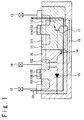
FIG. 1] FIG. 1 is a sectional view showing a configuration example of the semiconductor integrated circuit and the principle of occurrence of SEL. - [
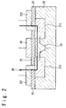
FIG. 2] FIG. 2 is a sectional view showing another configuration example of the semiconductor integrated circuit and the principle of occurrence of SEL, SEU or SET. - [
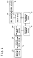
FIG. 3] FIG. 3 is a block diagram schematically showing a configuration example of the electronic device according to the present invention. - First, an important error which is caused in a semiconductor integrated device located under the environment exposed to radiation will be described.
-
FIG. 1 is a sectional view showing a configuration example of a semiconductor integrated circuit and a principle of occurrence of SEL. The configuration of the semiconductor integrated circuit shown inFIG. 1 will be described. - The semiconductor integrated circuit shown in
FIG. 1 has an N-type body region 10, a source 101, adrain 102, anoxide film 103 and a gate 104. These components work as a P-type MOS (Metal Oxide Semiconductor) FET (Field Effect Transistor). Apower supply terminal 12 is connected with the source 101 to supply a power supply voltage VDD. Asignal terminal 14 is connected with thedrain 102 to supply a signal voltage Pin. - The semiconductor integrated circuit shown in
FIG. 1 further has a P-type well 11, adrain 111, a source 112, an oxide film 113 and a gate 114. These components work as an N-type MOSFET. Aground terminal 13 is connected with the source 112 to supply a ground voltage VSS. - As in the semiconductor integrated circuit shown in
FIG. 1 , when the P-type MOSFET and the N-type MOSFET are formed to be adjacent to each other, aparasitic diode structure 15, parasiticbipolar transistor structures parasitic thyristor structure 18 and so on are formed, resulting in the operation of undesired functions. - In a configuration example shown in
FIG. 1 , aparasitic diode structure 15 exists in which thedrain 102 functions as an anode and the N-type body region 10 functions as a cathode. - The parasitic
bipolar transistor structure 16 exists, in which thedrain 102 functions as a P-type emitter, the P-type well 11 functions as a P-type collector and the N-type body region 10 functions as an N-type base. - Another parasitic
bipolar transistor structure 17 exists, in which the source 112 functions as an N-type emitter, the N-type body region 10 functions as an N-type collector and the P-type well 11 functions as a P-type base. - Moreover, the above-mentioned parasitic
bipolar transistor structure 16 and the other parasiticbipolar transistor structure 17 are combined to produce theparasitic thyristor structure 18. - When a charged particle with a high energy is incident on such a semiconductor integrated circuit, current 19 flows. The current 19 enters the semiconductor integrated circuit from the
power supply terminal 12 which applies the power supply voltage VDD to the N-type body region 10 and the source 101, passes through the N-type body region 10 and the P-type well 11, and goes out from theground terminal 13 which applies a ground voltage VSS to the P-type well 11 and the source 112. - Because this current 19 flows through the
parasitic thyristor structure 18, SEL occurs. The current 19 which accompanies SEL flows through an originally unintentional route, resulting in generation of an error in the operation of the semiconductor integrated circuit. -
FIG. 2 is a sectional view showing another configuration example of the semiconductor integrated circuit and a principle of occurrence of the SEU or SET. The structure of the semiconductor integrated circuit shown inFIG. 2 will be described. - The semiconductor integrated circuit shown in
FIG. 2 has a P-type body region 20, two N-type wells insulating layer 22, asource 231, adrain 232 and agate 24. These components operates as the N-type MOSFET. - In case of the semiconductor integrated circuit shown in
FIG. 2 , a parasiticbipolar transistor structure 25 exists in which one 211 of the two N-type wells functions as an N-type emitter, the other N-type well 212 functions as the N-type collector, and the P-type body region functions as the P-type base. - When a charged particle with a high energy is incident on such a semiconductor integrated circuit, a current 26 flows. The current 26 enters the semiconductor integrated circuit from the
drain 232, passes through the N-type well 212, the P-type body region 20 and the N-type well 211, and goes out from thesource 231. - Because this current 26 flows through the parasitic
bipolar transistor structure 25, SEU and SET occur. When SEU is caused in the semiconductor integrated circuit which functions as a memory, a flip-flop and so on, the inversion of the stored data can be caused. Also, when SET occurs in the semiconductor integrated circuit which functions as a logic circuit and so on, an undesired current and voltage occurs like a pulse so that a malfunction can be caused. - In the present invention, the tolerance to radiation is improved by using the phenomenon that the resistance of the semiconductor body region decreases through cooling a semiconductor integrated circuit. That is, the current generated when the charged particle is incident to the semiconductor integrated circuit becomes easier to pass through the semiconductor body region if the resistance of the semiconductor body region falls more. As a result, the value of the current which flows through the parasitic thyristor structure and the parasitic bipolar transistor structure becomes smaller. Here, according to the present invention, note that the redesigning of the semiconductor integrated circuit itself is unnecessary.
- Referring to the attached drawings, an embodiment to realize an electronic device according to the present invention will be described below.
-
FIG. 3 is a block diagram showing a configuration example of the electronic device according to the present invention. The configuration of the electronic device shown inFIG. 3 will be described. - The electronic device shown in
FIG. 3 has a semiconductor integratedcircuit 31, a cooling unit 32, aradiation detection unit 33 and atemperature measuring section 34. Here, as the semiconductor integratedcircuit 31, an optional semiconductor integrated circuit is available. - The cooling unit 32 contains a
cooling device 321, aheat conductor 322, athermal radiator 323 and a coolingdevice control section 324. As an example, thecooling device 321 may be a Peltier device and so on, andthermal radiator 323 may be a heat sink, an outer wall of an artificial satellite and so on. - The
radiation detection unit 33 contains aradiation detecting section 331 and a radiation detectingsection control section 332. - The connection relation of the components shown in
FIG. 3 will be described. Note that inFIG. 3 , an electric connection is shown by a single line and a thermal connection is shown by a double line. - The semiconductor integrated
circuit 31 and thecooling device 321 are thermally connected. Thecooling device 321 and theheat conductor 322 are thermally connected. Theheat conductor 322 andthermal radiator 323 are thermally connected. For example, when these thermal connections are established, it is desirable that the surface to be connected is brought into close contact through thermal grease, adhesive material and so on. - The semiconductor integrated
circuit 31 and thetemperature measuring section 34 are thermally connected. Here, thetemperature measuring section 34 may be built in the semiconductor integratedcircuit 31. Oppositely, when thetemperature measuring section 34 is independent from the semiconductor integratedcircuit 31, both of them may be brought into close contact, or thetemperature measuring section 34 may be arranged in a position apart from the semiconductor integratedcircuit 31 by a short distance. Moreover, onetemperature measuring section 34 may be provided to a plurality of semiconductor integratedcircuits 31. In any case, thetemperature measuring section 34 is arranged in the position where the temperature of semiconductor integratedcircuit 31 can be measured in a desired precision. - The output and input of the
radiation detecting section 331 are electrically connected with the input and output of the radiation detectingsection control unit 332, respectively. The other output and the other input of the radiation detectingsection control unit 332 are electrically connected with the input and output of the coolingdevice control section 324, respectively. The other input of the coolingdevice control section 324 is electrically connected with the output of thetemperature measuring section 34. The other output of the coolingdevice control section 324 is electrically connected with the input of thecooling device 321. Note that it is desirable for theradiation detecting section 331 to be arranged in a position which is near sufficiently from the semiconductor integratedcircuit 31 so that theradiation detecting section 331 can detect a radiation quantity which influences the semiconductor integratedcircuit 31 in a desired precision. - Each of the above-mentioned electric connections may be conducted with two wiring lines which are a combination of a signal line and a ground line. At this time, the
heat conductor 322 andthermal radiator 323 may be used as a part of the ground line. - An operation of each component shown in
FIG. 3 will be described. - The
cooling device 321 is controlled by the coolingdevice control unit 324 to cool the semiconductor integratedcircuit 31. Theheat conductor 322 transfers a heat quantity generated with this cooling from thecooling device 321 tothermal radiator 323. Thethermal radiator 323 radiates the heat quantity transferred from theheat conductor 322 toward the outside. - The
radiation detecting section 331 is controlled by the radiation detectingsection control section 332 to detect a radiation quantity. Theradiation detecting section 331 generates a signal indicating a detection result of the radiation quantity to transmit to the coolingdevice control section 324 through the radiation detectingsection control section 332. Note that the signal indicating the detection result of the radiation quantity may be directly communicated from theradiation detecting section 331 to the coolingdevice control section 324. - The
temperature measuring section 34 measures a temperature of the semiconductor integratedcircuit 31 itself or around it. Thetemperature measuring section 34 generates a signal indicting the measurement result of temperature toward the coolingdevice control section 324. - The operations of the cooling
device control section 324 and the radiation detectingsection control section 332 will be described in detail. When the electronic device according to the present invention is the above-mentioned artificial satellite as an example, it is necessary to control the power consumption so as to save it as much as possible. Especially, the Peltier device consumes much power to move a heat quantity from a cooling surface to a hot surface. Also, the power is consumed for the detection of the radiation quantity. - Therefore, the cooling
device control section 324 may control a cooling ability of thecooling device 321 based on a combination of the detected radiation quantity and the measured temperature. Also, the coolingdevice control section 324 may carry out the control operation of thecooling device 321 when the detected radiation quantity is higher than a predetermined threshold value, when the detected temperature is higher than a predetermined threshold value, or when the above two conditions are met. It is desirable that these operation conditions and specific threshold values can be set or changed appropriately according to the importance of the operation to be carried out by the semiconductor integratedcircuit 31. - Also, the radiation detecting
section control section 332 may control theradiation detecting section 331 to regularly detect the radiation quantity and may control it to detect the radiation only when the measured temperature is higher than the predetermined threshold value. - In this way, in the present invention, the tolerance to the radiation is improved by using the phenomenon that the resistance of the body region of the semiconductor integrated circuit falls without any alteration of the configuration of the existing semiconductor integrated circuit as the semiconductor integrated circuit is cooled. Moreover, by controlling the detection of the radiation quantity and the appropriately controlling to cool the semiconductor integrated circuit, the power consumed through these operations can be saved.
- Also, as a further application of this embodiment, a kit may be prepared which has components of the electronic device shown in
FIG. 3 except for the semiconductor integratedcircuit 31. If such a kit is loaded such that thecooling device 321 is brought into close contact to the surface of an existing semiconductor integrated circuit, the tolerance to radiation in the existing semiconductor integrated circuit can be improved. - The embodiments of the invention made by the inventors have been described. However, the present invention is not limited to the embodiments and various modifications are possible in a range without deviating from features of the present invention. Also, the features described in the embodiments may be combined in a range without contradicting technically.
-
- 10
- N-type body region
- 101
- source
- 102
- drain
- 103
- oxide film
- 104
- gates
- 11
- P-type well
- 111
- drain
- 112
- source
- 113
- oxide film
- 114
- gate
- 12
- power supply terminal
- 13
- ground terminal
- 14
- signal terminal
- 15
- parasitic diode structure
- 16
- parasitic transistor structure
- 17
- parasitic transistor structure
- 18
- parasitic thyristor structure
- 19
- SEL current
- 20
- P-type body region
- 211
- N-type well
- 212
- N-type well
- 22
- insulating layer
- 231
- source
- 232
- drain
- 24
- gate
- 25
- parasitic bipolar transistor structure
- 26
- SEU current, SEU current
- 31
- semiconductor integrated circuit
- 32
- cooling unit
- 321
- cooling device
- 322
- heat conductor
- 323
- thermal radiator
- 324
- cooling device control section
- 33
- radiation detection unit
- 331
- radiation detecting section
- 332
- radiation detecting section control section
- 34
- temperature measuring section
Claims (8)
- An electronic device comprising:an optional semiconductor integrated circuit;a radiation detection unit provided near the semiconductor integrated circuit to detect a radiation quantity; anda cooling unit configured to cool the semiconductor integrated circuit based on the detected radiation quantity.
- The electronic device according to claim 1, wherein the cooling unit comprises:a cooling device thermally connected with the semiconductor integrated circuit to absorb a heat quantity from the semiconductor integrated circuit;a heat conductor thermally connected with the cooling device to conduct the absorbed heat quantity;a thermal radiator thermally connected with the heat conductor to radiate the conducted heat quantity toward outside.
- The electronic device according to claim 2, further comprising:a temperature measuring section configured to measure a temperature of the semiconductor integrated circuit,wherein the cooling unit further comprises:a cooling device control section configured to control an operation of the cooling device such that the measured temperature falls within a predetermined range.
- The electronic device according to claim 3, wherein the radiation detection unit comprises:a radiation detecting section configured to detect the radiation quantity; anda radiation detecting section control section configured to control an operation of the radiation detecting section and generate a signal indicating the detected radiation quantity to transmit to the cooling device control section.
- A kit comprising:a radiation detection unit provided near an optional semiconductor integrated circuit to detect a radiation quantity; anda cooling unit attached to the semiconductor integrated circuit so as to be brought into close contact with the semiconductor integrated circuit and configured to cool the semiconductor integrated circuit based on the detected radiation quantity.
- The kit according to claim 5, wherein the cooling unit comprises:a cooling device thermally connected with the semiconductor integrated circuit to absorb a heat quantity from the semiconductor integrated circuit;a heat conductor thermally connected with the cooling unit to conduct the absorbed heat quantity; anda thermal radiator thermally connected with the heat conductor to radiate the conducted heat quantity toward outside.
- The kit according to claim 6, further comprising:a temperature measuring section configured to measure a temperature of the semiconductor integrated circuit,wherein the cooling unit further comprises:a cooling device control section configured to control an operation of the cooling unit such that the measured temperature falls within a predetermined range.
- The kit according to claim 7, wherein the radiation detection unit comprises:a radiation detecting section configured to detect a radiation quantity; anda radiation detecting section control section configured to control an operation of the radiation detecting section and to generate a signal indicating the detected radiation quantity to transmit to the cooling device control section.
Applications Claiming Priority (2)
| Application Number | Priority Date | Filing Date | Title |
|---|---|---|---|
| JP2014058801A JP6344938B2 (en) | 2014-03-20 | 2014-03-20 | Electronics |
| PCT/JP2015/058099 WO2015141737A1 (en) | 2014-03-20 | 2015-03-18 | Electronic apparatus |
Publications (3)
| Publication Number | Publication Date |
|---|---|
| EP3093884A1 true EP3093884A1 (en) | 2016-11-16 |
| EP3093884A4 EP3093884A4 (en) | 2017-04-26 |
| EP3093884B1 EP3093884B1 (en) | 2020-01-29 |
Family
ID=54144701
Family Applications (1)
| Application Number | Title | Priority Date | Filing Date |
|---|---|---|---|
| EP15765100.1A Active EP3093884B1 (en) | 2014-03-20 | 2015-03-18 | Electronic device |
Country Status (4)
| Country | Link |
|---|---|
| US (1) | US10002816B2 (en) |
| EP (1) | EP3093884B1 (en) |
| JP (1) | JP6344938B2 (en) |
| WO (1) | WO2015141737A1 (en) |
Families Citing this family (2)
| Publication number | Priority date | Publication date | Assignee | Title |
|---|---|---|---|---|
| CN108417571B (en) * | 2018-05-18 | 2024-08-13 | 北京时代华诺科技有限公司 | MOS control thyristor chip |
| CN110617885B (en) * | 2019-09-27 | 2020-11-24 | 衢州光明电力投资集团有限公司 | A method for measuring temperature of power equipment based on far-infrared imaging |
Family Cites Families (7)
| Publication number | Priority date | Publication date | Assignee | Title |
|---|---|---|---|---|
| JP3000688B2 (en) * | 1990-02-14 | 2000-01-17 | 株式会社日立製作所 | Radiation hardening protection device and artificial satellite for electronic circuit |
| US5270551A (en) | 1990-02-14 | 1993-12-14 | Hitachi, Ltd. | Method of and apparatus for protecting electronic circuit against radiation |
| US6173576B1 (en) | 1999-03-25 | 2001-01-16 | Intel Corporation | Cooling unit for an integrated circuit package |
| JP2002166898A (en) * | 2000-12-01 | 2002-06-11 | Mitsubishi Heavy Ind Ltd | Cooling device for space equipment |
| JP5351796B2 (en) | 2010-02-22 | 2013-11-27 | 三菱重工業株式会社 | Semiconductor circuit |
| EP2579239A4 (en) * | 2010-05-28 | 2016-01-20 | Nec Display Solutions Ltd | Projection display device |
| US8957385B2 (en) * | 2010-11-29 | 2015-02-17 | Saint-Gobain Ceramics & Plastics, Inc. | Radiation detection system, a radiation sensing unit, and methods of using the same |
-
2014
- 2014-03-20 JP JP2014058801A patent/JP6344938B2/en active Active
-
2015
- 2015-03-18 US US15/117,805 patent/US10002816B2/en active Active
- 2015-03-18 EP EP15765100.1A patent/EP3093884B1/en active Active
- 2015-03-18 WO PCT/JP2015/058099 patent/WO2015141737A1/en not_active Ceased
Also Published As
| Publication number | Publication date |
|---|---|
| EP3093884B1 (en) | 2020-01-29 |
| WO2015141737A1 (en) | 2015-09-24 |
| JP2015185596A (en) | 2015-10-22 |
| US10002816B2 (en) | 2018-06-19 |
| EP3093884A4 (en) | 2017-04-26 |
| JP6344938B2 (en) | 2018-06-20 |
| US20170011984A1 (en) | 2017-01-12 |
Similar Documents
| Publication | Publication Date | Title |
|---|---|---|
| JP5547429B2 (en) | Semiconductor device | |
| CN102195282B (en) | Current limiting circuit | |
| WO2021019539A1 (en) | On-die thermal sensing network for integrated circuits | |
| CN104967095B (en) | Thermal-shutdown circuit | |
| US20090033155A1 (en) | Semiconductor integrated circuits | |
| CN104967094B (en) | A kind of thermal-shutdown circuit | |
| US9875950B2 (en) | Semiconductor device | |
| Zhang et al. | Temperature dependence of soft-error rates for FF designs in 20-nm bulk planar and 16-nm bulk FinFET technologies | |
| CN103309389A (en) | Low pass filter circuit and voltage regulator | |
| US20100271739A1 (en) | Semiconductor integrated circuit having protection circuit capable of protecting against ESD and EOS | |
| US8947842B2 (en) | Temperature evaluation circuit | |
| US10002816B2 (en) | Electronic device | |
| EP3101686B1 (en) | Semiconductor integrated circuit device | |
| Tsai et al. | Active guard ring to improve latch-up immunity | |
| JP3132587B2 (en) | Power device overheat detection circuit | |
| TWI721045B (en) | Semiconductor component comprising a substrate and a first temperature measuring element, and method for determining a current flowing through a semiconductor component, and control unit for a vehicle | |
| US9804628B2 (en) | Reference voltage generator | |
| Gossner | Design for ESD protection at its limits | |
| Anashin et al. | Equipment and test results of the electronic components to SEE in the temperature range | |
| JP2016213981A (en) | Overheat protection circuit, semiconductor integrated circuit device using the same, and vehicle | |
| JP2009038186A (en) | Semiconductor device | |
| Du et al. | A double-threshold over-temperature protection circuit for smart power ICs | |
| US12598988B2 (en) | Integrated circuit device | |
| JP2024072439A (en) | Semiconductor Device | |
| US20140085758A1 (en) | Integrated circuit device and method of enabling thermal regulation within an integrated circuit device |
Legal Events
| Date | Code | Title | Description |
|---|---|---|---|
| PUAI | Public reference made under article 153(3) epc to a published international application that has entered the european phase |
Free format text: ORIGINAL CODE: 0009012 |
|
| 17P | Request for examination filed |
Effective date: 20160809 |
|
| AK | Designated contracting states |
Kind code of ref document: A1 Designated state(s): AL AT BE BG CH CY CZ DE DK EE ES FI FR GB GR HR HU IE IS IT LI LT LU LV MC MK MT NL NO PL PT RO RS SE SI SK SM TR |
|
| AX | Request for extension of the european patent |
Extension state: BA ME |
|
| RIC1 | Information provided on ipc code assigned before grant |
Ipc: H01L 27/144 20060101ALI20170316BHEP Ipc: G01T 7/00 20060101ALI20170316BHEP Ipc: H01L 21/822 20060101ALI20170316BHEP Ipc: B64G 1/50 20060101ALI20170316BHEP Ipc: H01L 27/04 20060101ALI20170316BHEP Ipc: H01L 23/34 20060101AFI20170316BHEP Ipc: H01L 27/092 20060101ALI20170316BHEP Ipc: H01L 23/367 20060101ALI20170316BHEP Ipc: B64G 1/54 20060101ALI20170316BHEP Ipc: G01T 1/24 20060101ALI20170316BHEP Ipc: G01J 5/00 20060101ALI20170316BHEP Ipc: H01L 23/38 20060101ALI20170316BHEP Ipc: F25B 21/02 20060101ALI20170316BHEP |
|
| A4 | Supplementary search report drawn up and despatched |
Effective date: 20170324 |
|
| DAV | Request for validation of the european patent (deleted) | ||
| DAX | Request for extension of the european patent (deleted) | ||
| REG | Reference to a national code |
Ref country code: DE Ref legal event code: R079 Ref document number: 602015046054 Country of ref document: DE Free format text: PREVIOUS MAIN CLASS: H01L0023340000 Ipc: B64G0001500000 |
|
| RIC1 | Information provided on ipc code assigned before grant |
Ipc: B64G 1/50 20060101AFI20190423BHEP Ipc: B64G 1/54 20060101ALI20190423BHEP Ipc: H01L 27/092 20060101ALI20190423BHEP Ipc: H01L 23/38 20060101ALI20190423BHEP Ipc: H01L 23/367 20060101ALI20190423BHEP Ipc: H01L 23/34 20060101ALN20190423BHEP Ipc: G01J 5/00 20060101ALI20190423BHEP Ipc: G01T 1/24 20060101ALI20190423BHEP Ipc: F25B 21/02 20060101ALN20190423BHEP Ipc: B64G 1/66 20060101ALI20190423BHEP |
|
| GRAP | Despatch of communication of intention to grant a patent |
Free format text: ORIGINAL CODE: EPIDOSNIGR1 |
|
| STAA | Information on the status of an ep patent application or granted ep patent |
Free format text: STATUS: GRANT OF PATENT IS INTENDED |
|
| INTG | Intention to grant announced |
Effective date: 20190605 |
|
| GRAS | Grant fee paid |
Free format text: ORIGINAL CODE: EPIDOSNIGR3 |
|
| GRAA | (expected) grant |
Free format text: ORIGINAL CODE: 0009210 |
|
| STAA | Information on the status of an ep patent application or granted ep patent |
Free format text: STATUS: THE PATENT HAS BEEN GRANTED |
|
| AK | Designated contracting states |
Kind code of ref document: B1 Designated state(s): AL AT BE BG CH CY CZ DE DK EE ES FI FR GB GR HR HU IE IS IT LI LT LU LV MC MK MT NL NO PL PT RO RS SE SI SK SM TR |
|
| REG | Reference to a national code |
Ref country code: GB Ref legal event code: FG4D |
|
| REG | Reference to a national code |
Ref country code: CH Ref legal event code: EP |
|
| REG | Reference to a national code |
Ref country code: AT Ref legal event code: REF Ref document number: 1228349 Country of ref document: AT Kind code of ref document: T Effective date: 20200215 |
|
| REG | Reference to a national code |
Ref country code: IE Ref legal event code: FG4D |
|
| REG | Reference to a national code |
Ref country code: DE Ref legal event code: R096 Ref document number: 602015046054 Country of ref document: DE |
|
| REG | Reference to a national code |
Ref country code: NL Ref legal event code: MP Effective date: 20200129 |
|
| PG25 | Lapsed in a contracting state [announced via postgrant information from national office to epo] |
Ref country code: RS Free format text: LAPSE BECAUSE OF FAILURE TO SUBMIT A TRANSLATION OF THE DESCRIPTION OR TO PAY THE FEE WITHIN THE PRESCRIBED TIME-LIMIT Effective date: 20200129 Ref country code: NO Free format text: LAPSE BECAUSE OF FAILURE TO SUBMIT A TRANSLATION OF THE DESCRIPTION OR TO PAY THE FEE WITHIN THE PRESCRIBED TIME-LIMIT Effective date: 20200429 Ref country code: FI Free format text: LAPSE BECAUSE OF FAILURE TO SUBMIT A TRANSLATION OF THE DESCRIPTION OR TO PAY THE FEE WITHIN THE PRESCRIBED TIME-LIMIT Effective date: 20200129 Ref country code: PT Free format text: LAPSE BECAUSE OF FAILURE TO SUBMIT A TRANSLATION OF THE DESCRIPTION OR TO PAY THE FEE WITHIN THE PRESCRIBED TIME-LIMIT Effective date: 20200621 |
|
| REG | Reference to a national code |
Ref country code: LT Ref legal event code: MG4D |
|
| PG25 | Lapsed in a contracting state [announced via postgrant information from national office to epo] |
Ref country code: IS Free format text: LAPSE BECAUSE OF FAILURE TO SUBMIT A TRANSLATION OF THE DESCRIPTION OR TO PAY THE FEE WITHIN THE PRESCRIBED TIME-LIMIT Effective date: 20200529 Ref country code: BG Free format text: LAPSE BECAUSE OF FAILURE TO SUBMIT A TRANSLATION OF THE DESCRIPTION OR TO PAY THE FEE WITHIN THE PRESCRIBED TIME-LIMIT Effective date: 20200429 Ref country code: GR Free format text: LAPSE BECAUSE OF FAILURE TO SUBMIT A TRANSLATION OF THE DESCRIPTION OR TO PAY THE FEE WITHIN THE PRESCRIBED TIME-LIMIT Effective date: 20200430 Ref country code: SE Free format text: LAPSE BECAUSE OF FAILURE TO SUBMIT A TRANSLATION OF THE DESCRIPTION OR TO PAY THE FEE WITHIN THE PRESCRIBED TIME-LIMIT Effective date: 20200129 Ref country code: LV Free format text: LAPSE BECAUSE OF FAILURE TO SUBMIT A TRANSLATION OF THE DESCRIPTION OR TO PAY THE FEE WITHIN THE PRESCRIBED TIME-LIMIT Effective date: 20200129 Ref country code: HR Free format text: LAPSE BECAUSE OF FAILURE TO SUBMIT A TRANSLATION OF THE DESCRIPTION OR TO PAY THE FEE WITHIN THE PRESCRIBED TIME-LIMIT Effective date: 20200129 |
|
| PG25 | Lapsed in a contracting state [announced via postgrant information from national office to epo] |
Ref country code: NL Free format text: LAPSE BECAUSE OF FAILURE TO SUBMIT A TRANSLATION OF THE DESCRIPTION OR TO PAY THE FEE WITHIN THE PRESCRIBED TIME-LIMIT Effective date: 20200129 |
|
| PG25 | Lapsed in a contracting state [announced via postgrant information from national office to epo] |
Ref country code: DK Free format text: LAPSE BECAUSE OF FAILURE TO SUBMIT A TRANSLATION OF THE DESCRIPTION OR TO PAY THE FEE WITHIN THE PRESCRIBED TIME-LIMIT Effective date: 20200129 Ref country code: SM Free format text: LAPSE BECAUSE OF FAILURE TO SUBMIT A TRANSLATION OF THE DESCRIPTION OR TO PAY THE FEE WITHIN THE PRESCRIBED TIME-LIMIT Effective date: 20200129 Ref country code: EE Free format text: LAPSE BECAUSE OF FAILURE TO SUBMIT A TRANSLATION OF THE DESCRIPTION OR TO PAY THE FEE WITHIN THE PRESCRIBED TIME-LIMIT Effective date: 20200129 Ref country code: MC Free format text: LAPSE BECAUSE OF FAILURE TO SUBMIT A TRANSLATION OF THE DESCRIPTION OR TO PAY THE FEE WITHIN THE PRESCRIBED TIME-LIMIT Effective date: 20200129 Ref country code: SK Free format text: LAPSE BECAUSE OF FAILURE TO SUBMIT A TRANSLATION OF THE DESCRIPTION OR TO PAY THE FEE WITHIN THE PRESCRIBED TIME-LIMIT Effective date: 20200129 Ref country code: CZ Free format text: LAPSE BECAUSE OF FAILURE TO SUBMIT A TRANSLATION OF THE DESCRIPTION OR TO PAY THE FEE WITHIN THE PRESCRIBED TIME-LIMIT Effective date: 20200129 Ref country code: ES Free format text: LAPSE BECAUSE OF FAILURE TO SUBMIT A TRANSLATION OF THE DESCRIPTION OR TO PAY THE FEE WITHIN THE PRESCRIBED TIME-LIMIT Effective date: 20200129 Ref country code: RO Free format text: LAPSE BECAUSE OF FAILURE TO SUBMIT A TRANSLATION OF THE DESCRIPTION OR TO PAY THE FEE WITHIN THE PRESCRIBED TIME-LIMIT Effective date: 20200129 Ref country code: LT Free format text: LAPSE BECAUSE OF FAILURE TO SUBMIT A TRANSLATION OF THE DESCRIPTION OR TO PAY THE FEE WITHIN THE PRESCRIBED TIME-LIMIT Effective date: 20200129 |
|
| REG | Reference to a national code |
Ref country code: CH Ref legal event code: PL Ref country code: DE Ref legal event code: R097 Ref document number: 602015046054 Country of ref document: DE |
|
| REG | Reference to a national code |
Ref country code: AT Ref legal event code: MK05 Ref document number: 1228349 Country of ref document: AT Kind code of ref document: T Effective date: 20200129 |
|
| PLBE | No opposition filed within time limit |
Free format text: ORIGINAL CODE: 0009261 |
|
| STAA | Information on the status of an ep patent application or granted ep patent |
Free format text: STATUS: NO OPPOSITION FILED WITHIN TIME LIMIT |
|
| REG | Reference to a national code |
Ref country code: BE Ref legal event code: MM Effective date: 20200331 |
|
| PG25 | Lapsed in a contracting state [announced via postgrant information from national office to epo] |
Ref country code: LU Free format text: LAPSE BECAUSE OF NON-PAYMENT OF DUE FEES Effective date: 20200318 |
|
| 26N | No opposition filed |
Effective date: 20201030 |
|
| PG25 | Lapsed in a contracting state [announced via postgrant information from national office to epo] |
Ref country code: IE Free format text: LAPSE BECAUSE OF NON-PAYMENT OF DUE FEES Effective date: 20200318 Ref country code: LI Free format text: LAPSE BECAUSE OF NON-PAYMENT OF DUE FEES Effective date: 20200331 Ref country code: IT Free format text: LAPSE BECAUSE OF FAILURE TO SUBMIT A TRANSLATION OF THE DESCRIPTION OR TO PAY THE FEE WITHIN THE PRESCRIBED TIME-LIMIT Effective date: 20200129 Ref country code: CH Free format text: LAPSE BECAUSE OF NON-PAYMENT OF DUE FEES Effective date: 20200331 Ref country code: AT Free format text: LAPSE BECAUSE OF FAILURE TO SUBMIT A TRANSLATION OF THE DESCRIPTION OR TO PAY THE FEE WITHIN THE PRESCRIBED TIME-LIMIT Effective date: 20200129 |
|
| PG25 | Lapsed in a contracting state [announced via postgrant information from national office to epo] |
Ref country code: SI Free format text: LAPSE BECAUSE OF FAILURE TO SUBMIT A TRANSLATION OF THE DESCRIPTION OR TO PAY THE FEE WITHIN THE PRESCRIBED TIME-LIMIT Effective date: 20200129 Ref country code: BE Free format text: LAPSE BECAUSE OF NON-PAYMENT OF DUE FEES Effective date: 20200331 Ref country code: PL Free format text: LAPSE BECAUSE OF FAILURE TO SUBMIT A TRANSLATION OF THE DESCRIPTION OR TO PAY THE FEE WITHIN THE PRESCRIBED TIME-LIMIT Effective date: 20200129 |
|
| PG25 | Lapsed in a contracting state [announced via postgrant information from national office to epo] |
Ref country code: TR Free format text: LAPSE BECAUSE OF FAILURE TO SUBMIT A TRANSLATION OF THE DESCRIPTION OR TO PAY THE FEE WITHIN THE PRESCRIBED TIME-LIMIT Effective date: 20200129 Ref country code: MT Free format text: LAPSE BECAUSE OF FAILURE TO SUBMIT A TRANSLATION OF THE DESCRIPTION OR TO PAY THE FEE WITHIN THE PRESCRIBED TIME-LIMIT Effective date: 20200129 Ref country code: CY Free format text: LAPSE BECAUSE OF FAILURE TO SUBMIT A TRANSLATION OF THE DESCRIPTION OR TO PAY THE FEE WITHIN THE PRESCRIBED TIME-LIMIT Effective date: 20200129 |
|
| PG25 | Lapsed in a contracting state [announced via postgrant information from national office to epo] |
Ref country code: MK Free format text: LAPSE BECAUSE OF FAILURE TO SUBMIT A TRANSLATION OF THE DESCRIPTION OR TO PAY THE FEE WITHIN THE PRESCRIBED TIME-LIMIT Effective date: 20200129 Ref country code: AL Free format text: LAPSE BECAUSE OF FAILURE TO SUBMIT A TRANSLATION OF THE DESCRIPTION OR TO PAY THE FEE WITHIN THE PRESCRIBED TIME-LIMIT Effective date: 20200129 |
|
| PGFP | Annual fee paid to national office [announced via postgrant information from national office to epo] |
Ref country code: GB Payment date: 20260202 Year of fee payment: 12 |
|
| PGFP | Annual fee paid to national office [announced via postgrant information from national office to epo] |
Ref country code: DE Payment date: 20260128 Year of fee payment: 12 |
|
| PGFP | Annual fee paid to national office [announced via postgrant information from national office to epo] |
Ref country code: FR Payment date: 20260209 Year of fee payment: 12 |