EP3091606A1 - Antenna for wireless communications - Google Patents
Antenna for wireless communications Download PDFInfo
- Publication number
- EP3091606A1 EP3091606A1 EP16165720.0A EP16165720A EP3091606A1 EP 3091606 A1 EP3091606 A1 EP 3091606A1 EP 16165720 A EP16165720 A EP 16165720A EP 3091606 A1 EP3091606 A1 EP 3091606A1
- Authority
- EP
- European Patent Office
- Prior art keywords
- core
- windings
- contact
- conductive path
- antenna
- Prior art date
- Legal status (The legal status is an assumption and is not a legal conclusion. Google has not performed a legal analysis and makes no representation as to the accuracy of the status listed.)
- Granted
Links
Images


Classifications
-
- H—ELECTRICITY
- H01—ELECTRIC ELEMENTS
- H01Q—ANTENNAS, i.e. RADIO AERIALS
- H01Q1/00—Details of, or arrangements associated with, antennas
- H01Q1/36—Structural form of radiating elements, e.g. cone, spiral, umbrella; Particular materials used therewith
-
- G—PHYSICS
- G06—COMPUTING OR CALCULATING; COUNTING
- G06K—GRAPHICAL DATA READING; PRESENTATION OF DATA; RECORD CARRIERS; HANDLING RECORD CARRIERS
- G06K19/00—Record carriers for use with machines and with at least a part designed to carry digital markings
- G06K19/06—Record carriers for use with machines and with at least a part designed to carry digital markings characterised by the kind of the digital marking, e.g. shape, nature, code
- G06K19/067—Record carriers with conductive marks, printed circuits or semiconductor circuit elements, e.g. credit or identity cards also with resonating or responding marks without active components
- G06K19/07—Record carriers with conductive marks, printed circuits or semiconductor circuit elements, e.g. credit or identity cards also with resonating or responding marks without active components with integrated circuit chips
- G06K19/077—Constructional details, e.g. mounting of circuits in the carrier
- G06K19/07749—Constructional details, e.g. mounting of circuits in the carrier the record carrier being capable of non-contact communication, e.g. constructional details of the antenna of a non-contact smart card
- G06K19/07773—Antenna details
- G06K19/07777—Antenna details the antenna being of the inductive type
- G06K19/07779—Antenna details the antenna being of the inductive type the inductive antenna being a coil
- G06K19/07781—Antenna details the antenna being of the inductive type the inductive antenna being a coil the coil being fabricated in a winding process
-
- G—PHYSICS
- G06—COMPUTING OR CALCULATING; COUNTING
- G06K—GRAPHICAL DATA READING; PRESENTATION OF DATA; RECORD CARRIERS; HANDLING RECORD CARRIERS
- G06K19/00—Record carriers for use with machines and with at least a part designed to carry digital markings
- G06K19/06—Record carriers for use with machines and with at least a part designed to carry digital markings characterised by the kind of the digital marking, e.g. shape, nature, code
- G06K19/067—Record carriers with conductive marks, printed circuits or semiconductor circuit elements, e.g. credit or identity cards also with resonating or responding marks without active components
- G06K19/07—Record carriers with conductive marks, printed circuits or semiconductor circuit elements, e.g. credit or identity cards also with resonating or responding marks without active components with integrated circuit chips
- G06K19/077—Constructional details, e.g. mounting of circuits in the carrier
- G06K19/07749—Constructional details, e.g. mounting of circuits in the carrier the record carrier being capable of non-contact communication, e.g. constructional details of the antenna of a non-contact smart card
- G06K19/07773—Antenna details
- G06K19/07786—Antenna details the antenna being of the HF type, such as a dipole
-
- H—ELECTRICITY
- H01—ELECTRIC ELEMENTS
- H01Q—ANTENNAS, i.e. RADIO AERIALS
- H01Q1/00—Details of, or arrangements associated with, antennas
- H01Q1/12—Supports; Mounting means
- H01Q1/22—Supports; Mounting means by structural association with other equipment or articles
- H01Q1/2208—Supports; Mounting means by structural association with other equipment or articles associated with components used in interrogation type services, i.e. in systems for information exchange between an interrogator/reader and a tag/transponder, e.g. in Radio Frequency Identification [RFID] systems
- H01Q1/2225—Supports; Mounting means by structural association with other equipment or articles associated with components used in interrogation type services, i.e. in systems for information exchange between an interrogator/reader and a tag/transponder, e.g. in Radio Frequency Identification [RFID] systems used in active tags, i.e. provided with its own power source or in passive tags, i.e. deriving power from RF signal
-
- H—ELECTRICITY
- H01—ELECTRIC ELEMENTS
- H01Q—ANTENNAS, i.e. RADIO AERIALS
- H01Q1/00—Details of, or arrangements associated with, antennas
- H01Q1/27—Adaptation for use in or on movable bodies
- H01Q1/273—Adaptation for carrying or wearing by persons or animals
-
- H—ELECTRICITY
- H01—ELECTRIC ELEMENTS
- H01Q—ANTENNAS, i.e. RADIO AERIALS
- H01Q1/00—Details of, or arrangements associated with, antennas
- H01Q1/52—Means for reducing coupling between antennas; Means for reducing coupling between an antenna and another structure
-
- H—ELECTRICITY
- H01—ELECTRIC ELEMENTS
- H01Q—ANTENNAS, i.e. RADIO AERIALS
- H01Q7/00—Loop antennas with a substantially uniform current distribution around the loop and having a directional radiation pattern in a plane perpendicular to the plane of the loop
Definitions
- RFID systems can include an RFID reader device (also referred to as a "reader device” or just a “reader”) that generates an RF signal that can be received and used by an RFID tag device (also referred to as a "tag device” or just a “tag”).
- the tag device can, in some instances, harvest power from the received RF signal and also transmit data back to the reader by modulating the RF signal.
- the size and ruggedness of tags allows for the use of tags in a number of different applications. One such area includes mobile technologies, and more specifically, wearable technologies.
- Various example embodiments are directed to an apparatus or device that includes an antenna structure with a core shaped as a toroid that is designed to be worn on a human digit.
- a first and second contact are located on the core.
- a conductive path connects the first contact and the second contact and includes a first set of windings that traverse a circumference of the core in a substantially parallel manner; and a second set of windings that traverse the circumference of the core in a substantially parallel manner.
- the windings are such that, from a vantage point exterior to the core, the first set of windings is substantially perpendicular to the second set of windings.
- Embodiments are directed toward a system that includes an implantable circuit that includes a wireless communication circuit.
- a core is shaped as toroid and is designed with an exterior and an interior with a respective circumference that is designed to be worn on a human digit.
- a conductive path that includes a first winding that traverses the toroid while alternating between the exterior and the interior for respective portions of the core; and a second winding that traverses the toroid while alternating between the exterior and the interior for respective portions of the core in a manner that the first winding is on the interior for portions where the second winding is on the exterior.
- a method for creating an antenna structure includes creating a core shaped as a toroid that is designed to be worn on a human digit.
- a first contact and a second contact are applied on the core.
- a conductive path is created that connects the first contact and the second contact.
- the path is created by: alternating between a first winding pattern that traverses a circumference of the core in a first substantially parallel manner; and a second winding pattern that traverse the circumference of the core in a second substantially parallel manner.
- the winding patterns are such that, from a vantage point exterior to the core, first and second winding patterns are substantially perpendicular to one another.
- aspects of the present disclosure are believed to be applicable to a variety of different types of apparatuses, systems and methods involving wireless communications and specialized antennas. Aspects of the present disclosure have been shown to be beneficial when used in the context of wearable wireless devices. For example, one or more embodiments may be adapted to an antenna that is designed to be worn on a digit (finger or toe) of a person. While not necessarily so limited, various aspects may be appreciated through a discussion of examples using such contexts.
- Embodiments of the present disclosures are directed toward a wearable antenna that is designed to be worn on a digit of a person, while also being configured to be used for wireless communication for different rotations of the antenna relative to another device and the other device's corresponding antenna.
- the wearable antenna can be configured such that, or any rotation, at least one conductive path (e.g ., a wire) is at about a 45° angle, or greater, relative to a conductive path of the other antenna and relative to a corresponding vantage point from the other antenna.
- a wearable antenna can have a toroid-shaped core.
- An opening in the core can be designed to allow the antenna to be worn on a digit of a person.
- the antenna includes a conductive path with multiple windings about the core, where each winding represents one traversal of the circumference of the core. Together, the multiple windings represent a single conductive path that is designed to allow for current to flow from one end of the path to the other end of the path.
- Each end of the path can be connected to contacts and a wireless (e . g ., HF-RFID) communication circuit.
- the windings of a wearable antenna can be separated into two different sets of windings, where each winding traverses a circumference of the core by alternating between an internal portion - forming the opening, and an external portion of the core.
- each of the windings in the same set can follow an antenna pattern in which the conductive paths, or wires, of the windings are substantially parallel to one another.
- the orientations of the windings from the different sets can be substantially perpendicular, when viewed from a vantage point that is exterior to the core.
- Wearable electronic products can be used for a variety of purposes including, but not limited to, the medical field (e . g ., wearable hearing aids and pacemakers).
- NFC-capable devices can be used for security applications, such as unlocking mobile phones, and sharing information like Wi-Fi passwords, links to websites, contact information, etc.
- Wearable technologies also can be used in automation and security systems such as car and home security systems.
- Security capabilities can be hampered by the use of more than one integrated circuit (IC) or the addition of security elements within an IC.
- IC integrated circuit
- the addition of a secure element to NFC controller can consume more chip space, making the chip bigger, and increase the power consumption.
- the NFC controller has limited power (e.g ., powered by an RF signal from a reader device)
- increases in power demands can negatively impact the read range.
- a particular type of wearable technology are rings that can be worn by a person and used as an antenna. NFC rings for wearable technology applications can cause security to suffer from problems with maintaining communication with the reader antenna while the ring is worn, and may need multiple different antenna patterns and designs for different sizes of rings.
- Various embodiments of the present disclosure utilize an antenna structure that uses polarization to reduce the connection loss due to rotation, and include an antenna layout design that can accommodate different finger sizes for a single structure. Particular embodiments relate to a design that is relatively thin and has a high Q factor value.
- Circular loop antennas can be designed for reliable use in the ultra-high frequency (UHF) RFID domain.
- UHF ultra-high frequency
- a ring antenna can be used with a microcontroller circuit, such as a secure authentication microcontroller.
- the secure authentication microcontroller may, for example, be configured to communicate one or more secure codes to an RFID reader device. This might, for example, validate the reader device before making patient data available ( e . g ., in the context of an implantable medical device). In another example, the authentication could be used to provide access to functions of the RFID reader device ( e . g ., automated access to a cellular smart phone).
- the ring antenna can be used for applications in high frequency (HF) range with low power/small signals. Accordingly, losses related to physical dimension and field distributions can largely be ignored, as they are mostly relevant to high power devices. Consistent with embodiments, the core or the ring carrier can be constructed from non-magnetic material and there is no need to consider core losses and induced eddy current.
- FIG. 1 depicts a block diagram of a system for RF communication, consistent with embodiments of the present disclosure.
- a reader device 116 can include a communication circuit 118 and a control circuit 120 that are designed to establish communication with one or more tag devices.
- the control circuit 120 can include a microcontroller and a memory circuit and the communication circuit 118 can include a transceiver circuit and an antenna.
- the reader device can be configured to communicate with HF RFID capable devices.
- a tag device 100 can be configured to communicate with the reader device 116.
- the tag device can include a control circuit 102 and a communication circuit 106. Consistent with embodiments, the tag device 100 can be configured to all, or some, of the circuits powered by an RF signal received from a reader device.
- the communication circuit 106 can be connected to a toroid-shaped antenna 110 by a set of wires or similar conductors 108.
- the antenna 110 can be designed to be worn on a human digit.
- standard ring sizes for fingers can have an inner circumference that ranges from 1.44 inches to 3.05 inches (i.e., from 3.6576 cm to 7.747 cm).
- the antenna 110 can be configured so it can receive a signal from reader 106 while being rotated in multiple directions 112, 114.
- the antenna can be constructed by creating a conductive path that follows a pattern for which at least a portion of the conductive path is not parallel with the direction of flux from the antenna reader for any particular orientation.
- Circuit diagram 124 depicts a small signal equivalent circuit for the tag device 104 and antenna 110.
- the antenna pattern and core structure can each be designed based upon a number of factors. For instance, the flux density varies in reverse proportion with the ring radius. This can result in the magnetic field being significantly higher on the inner edge of the core rather than the outer portion of the toroid. Accordingly, various embodiments are directed toward keeping the width of the toroid core (or carrier) as thin as possible to help provide a uniform flux density.
- a small ratio of outer diameter over inner diameter (OD/ID) also prevents small thermal gradients between different portions of the core. Although this factor can often be neglected for the small signals, thermal gradients can still have an effect, such as where the temperature varies rapidly over time.
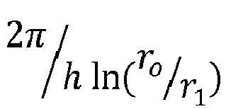
- C 1 and C 2 represent core constants that are computed for toroidal cores in terms of core height (h), and inner (n) and outer (r o ) radii of the core, where 2 ⁇ / h ln r o / r 1 and 2 ⁇ 1 / r i ⁇ 1 / r o / h 2 ln 3 r 0 / r 1 , respectively.
- reducing the ratio of the outer diameter to the inner diameter can reduce adverse effects resulting from variations in flux density within the core. Accordingly, it can be helpful to use a very thin core.
- V rms 2 ⁇ NA e B m ⁇
- V rms and B m are the root mean square (rms) values of the induced voltage and the peak and the peak value of the sinusoidal flux density, respectively. Since the voltage across the inductor in the series model is determined by voltage divider between the resistor and inductor, the flux density in the core is not directly related to the excitation voltage.
- each winding on the core wraps fully around the circumference of the toroid.
- a uniform winding reduces the amount of flux that leaves the core, and thus provides for a more uniform flux density.
- View 126 shows a ring that is segmented into four equal size quadrants sequentially numbered as I, II, III, and IV.
- Embodiments are directed toward a solution in which, for example, the pattern can be designed to have conductive paths on the exterior side of the ring that are substantially perpendicular to conductive paths on the interior of the ring, relative to a line passing through the center of the opening for the toroid.
- FIG. 2 depicts a top down view 200 of an antenna pattern, consistent with embodiments of the present disclosure.
- the antenna pattern 200 includes a plurality of windings that each traverse the circumference of the toroid core, which is not shown to allow for the windings on both sides of the core to be visible.
- Contact points, or terminals, 202 and 204 can be connected to respective ends of the conductive path formed by the windings.
- a transceiver circuit for a tag device can be connected across the terminals 202 and 204.
- FIG. 2 A portion of a first set of two windings, 206 and 208, are circled in FIG. 2 .
- the directional arrows indicate a possible direction of current for reference relative to the different windings (although the current direction can be reversed, which would result in a corresponding reversal in each winding).
- the physical orientation of the windings 206 and 208 are substantially parallel to one another, resulting in the direction of current flow also being substantially parallel with respect to each winding.
- the windings 206 and 208 are depicted as being on the top portion of the core (i.e., extending out of the page toward the viewer) at the circled location.
- a portion of a second set of two windings, 210 and 212, are also circled in FIG. 2 .
- the directional arrows again indicate a direction of current for reference relative to the different windings.
- the physical orientation of the windings 210 and 212 are substantially parallel to one another, resulting in the direction of current flow also being substantially parallel with respect to each winding.
- the physical orientation of the windings 210 and 212 is, however, substantially perpendicular to the windings 206 and 208, relative to the vantage point of the viewer of the figure.
- the windings 210 and 212 are depicted as being on the bottom portion of the core at the circled location.
- the core is designed to be relatively thin, and thus, either (or both) set of the windings can contribute to an inductive coupling between the tag and reader.
- View 220 shows a number of possible orientations and corresponding induced currents from windings of two different sets of windings.
- I can represent the current through an antenna (reader) wire of the reader device, while I 1 can correspond to current induced in windings 210 or 212, and I 2 can correspond to current induced in winding 206.
- the windings corresponding to I 1 and I 2 are shown with a directional arrow that corresponds to the directional arrow in view 200.
- the current direction may be in the opposite direction for certain orientations depicted in view 220.
- at least one of the antenna wires will be inductively coupled to the reader wire for all orientations.
- the other wire will be substantially perpendicular and therefore maximally coupled (where maximum coupling is with consideration to physical orientation only).
- FIG. 3 shows a side view 300 of an antenna structure, consistent with embodiments of the present disclosure. Consistent with FIG. 2 , the antenna structure is shown without the core present. Windings 302 and 304 form part of a first set of windings that are on the outside of the core, relative to the central opening for a digit of a person. Windings 306 and 308 form part of a second set of windings that are on the inside of the core. The orientations between the two sets of windings are similar to those described in connection with FIG. 2 in that windings of the same set are substantially perpendicular and windings of different sets are substantially perpendicular, relative to a particular vantage point.
- FIGs. 2 and 3 shows ten different windings.
- Various embodiments can include more or less windings depending upon the considerations of the particular implementation.
- the considerations can include, but are not necessarily limited to, communication frequencies, wireless signal strength of the reader device, limitations of the communication circuitry for the tag device, and cost.
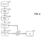
- FIG. 4 depicts a flow diagram for creating an antenna structure, consistent with embodiments of the present disclosure.
- a toroid-shaped core that is designed to wear on a digit of a person can be created, per block 402.
- the core can be non-magnetic and have an opening sufficient to be worn as a ring.
- Two contacts can be added to the core, per blocks 404 and 406.
- the contacts can be added at different times depending upon the particular implementation and manufacturing process. For instance, the contacts can be added to the core before, after, or during, the application of the windings.
- the contacts can be a pad or part of a physical connector that a wire, or similar conductor, can be attached using solder, physical connectors, and combinations thereof.
- a conductive path according to a first pattern set can be applied to the core, per block 408.
- the first part of conductive path can follow the first pattern and wrap round the inside and outside of the core while traversing the circumference of the core once.
- the conductive path can continued to be applied to the core according to a second pattern set, per block 410.
- the second pattern can be configured such that from different vantage points external to the core, the winding corresponding to the second pattern is substantially perpendicular to the previously-applied winding, which corresponds to first pattern.
- the conductive path can be applied by a printing process in which conductor material is applied to the core. Wire or similar conductor material can also be applied following the antenna pattern.
- a “block” (also sometimes “logic circuitry” or “module”) is a circuit that carries out one or more of these or related operations/activities (e . g ., performing secure authentication and carrying out related RFID communications).
- one or more modules or blocks are discrete logic circuits or programmable logic circuits configured and arranged for implementing these operations/activities, as in the circuit modules shown in FIG. 1 . The operations may be carried out in a logic circuit programmed to operate the indicated steps.
- such a programmable circuit is one or more computer circuits programmed to execute a set (or sets) of stored instructions (and/or configuration data).
- the instructions (and/or configuration data) can be in the form of firmware or software stored in and accessible from a memory (circuit).
- the various embodiments described herein may be combined in certain embodiments, and various aspects of individual embodiments may be implemented as separate embodiments.
- Certain embodiments are directed to a computer program product (e . g ., nonvolatile memory device), which includes a machine or computer-readable medium having stored instructions thereon which may be executed by a computer (or other electronic device) to perform one or more operations/activities disclosed herein.
- a computer program product e . g ., nonvolatile memory device
Landscapes
- Engineering & Computer Science (AREA)
- Computer Networks & Wireless Communication (AREA)
- Computer Hardware Design (AREA)
- Microelectronics & Electronic Packaging (AREA)
- Physics & Mathematics (AREA)
- General Physics & Mathematics (AREA)
- Theoretical Computer Science (AREA)
- Near-Field Transmission Systems (AREA)
- Support Of Aerials (AREA)
Abstract
Description
- Near field communication (NFC) and high frequency (HF) radio frequency identification (RFID), has rapidly grown for commercial applications such as peer-to-peer, payment, and card emulation. RFID systems can include an RFID reader device (also referred to as a "reader device" or just a "reader") that generates an RF signal that can be received and used by an RFID tag device (also referred to as a "tag device" or just a "tag"). The tag device can, in some instances, harvest power from the received RF signal and also transmit data back to the reader by modulating the RF signal. The size and ruggedness of tags allows for the use of tags in a number of different applications. One such area includes mobile technologies, and more specifically, wearable technologies.
- While various approaches have been implemented for wearable RFID devices, such devices may be susceptible to practical issues with establishing and maintaining wireless communication with an RFID reader due to antenna orientation and other problems. These issues can be particularly relevant to certain applications, such as implantable tag devices. These and other matters have presented challenges to communications and related aspects such as antenna orientations, for a variety of applications.
- Various example embodiments are directed to an apparatus or device that includes an antenna structure with a core shaped as a toroid that is designed to be worn on a human digit. A first and second contact are located on the core. A conductive path connects the first contact and the second contact and includes a first set of windings that traverse a circumference of the core in a substantially parallel manner; and a second set of windings that traverse the circumference of the core in a substantially parallel manner. The windings are such that, from a vantage point exterior to the core, the first set of windings is substantially perpendicular to the second set of windings.
- Embodiments are directed toward a system that includes an implantable circuit that includes a wireless communication circuit. A core is shaped as toroid and is designed with an exterior and an interior with a respective circumference that is designed to be worn on a human digit. A conductive path that includes a first winding that traverses the toroid while alternating between the exterior and the interior for respective portions of the core; and a second winding that traverses the toroid while alternating between the exterior and the interior for respective portions of the core in a manner that the first winding is on the interior for portions where the second winding is on the exterior.
- According to certain embodiments, a method for creating an antenna structure includes creating a core shaped as a toroid that is designed to be worn on a human digit. A first contact and a second contact are applied on the core. A conductive path is created that connects the first contact and the second contact. The path is created by: alternating between a first winding pattern that traverses a circumference of the core in a first substantially parallel manner; and a second winding pattern that traverse the circumference of the core in a second substantially parallel manner. The winding patterns are such that, from a vantage point exterior to the core, first and second winding patterns are substantially perpendicular to one another.
- The above discussion/summary is not intended to describe each embodiment or every implementation of the present disclosure. The figures and detailed description that follow also exemplify various embodiments.
- Various example embodiments may be more completely understood in consideration of the following detailed description and in connection with the accompanying drawings, in which:
-
FIG. 1 depicts a block diagram of a system for RF communication, consistent with embodiments of the present disclosure; -
FIG. 2 depicts a top downview 200 of an antenna pattern, consistent with embodiments of the present disclosure; -
FIG. 3 shows aside view 300 of an antenna structure, consistent with embodiments of the present disclosure; and -
FIG. 4 depicts a flow diagram for creating an antenna structure, consistent with embodiments of the present disclosure. - While various embodiments discussed herein are amenable to modifications and alternative forms, aspects thereof have been shown by way of example in the drawings and will be described in detail. It should be understood, however, that the intention is not to limit the disclosure to the particular embodiments described. On the contrary, the intention is to cover all modifications, equivalents, and alternatives falling within the scope of the disclosure including aspects defined in the claims. In addition, the term "example" as used throughout this application is only by way of illustration, and not limitation.
- Aspects of the present disclosure are believed to be applicable to a variety of different types of apparatuses, systems and methods involving wireless communications and specialized antennas. Aspects of the present disclosure have been shown to be beneficial when used in the context of wearable wireless devices. For example, one or more embodiments may be adapted to an antenna that is designed to be worn on a digit (finger or toe) of a person. While not necessarily so limited, various aspects may be appreciated through a discussion of examples using such contexts.
- Embodiments of the present disclosures are directed toward a wearable antenna that is designed to be worn on a digit of a person, while also being configured to be used for wireless communication for different rotations of the antenna relative to another device and the other device's corresponding antenna. For instance, the wearable antenna can be configured such that, or any rotation, at least one conductive path (e.g., a wire) is at about a 45° angle, or greater, relative to a conductive path of the other antenna and relative to a corresponding vantage point from the other antenna.
- Consistent with certain embodiments, a wearable antenna can have a toroid-shaped core. An opening in the core can be designed to allow the antenna to be worn on a digit of a person. The antenna includes a conductive path with multiple windings about the core, where each winding represents one traversal of the circumference of the core. Together, the multiple windings represent a single conductive path that is designed to allow for current to flow from one end of the path to the other end of the path. Each end of the path can be connected to contacts and a wireless (e.g., HF-RFID) communication circuit.
- Consistent with some embodiments, the windings of a wearable antenna can be separated into two different sets of windings, where each winding traverses a circumference of the core by alternating between an internal portion - forming the opening, and an external portion of the core. As discussed in more detail herein, each of the windings in the same set can follow an antenna pattern in which the conductive paths, or wires, of the windings are substantially parallel to one another. The orientations of the windings from the different sets, however, can be substantially perpendicular, when viewed from a vantage point that is exterior to the core.
- Wearable electronic products can be used for a variety of purposes including, but not limited to, the medical field (e.g., wearable hearing aids and pacemakers). NFC-capable devices can be used for security applications, such as unlocking mobile phones, and sharing information like Wi-Fi passwords, links to websites, contact information, etc. Wearable technologies also can be used in automation and security systems such as car and home security systems.
- Security capabilities can be hampered by the use of more than one integrated circuit (IC) or the addition of security elements within an IC. For instance, the addition of a secure element to NFC controller can consume more chip space, making the chip bigger, and increase the power consumption. For applications in which the NFC controller has limited power (e.g., powered by an RF signal from a reader device), increases in power demands can negatively impact the read range. A particular type of wearable technology are rings that can be worn by a person and used as an antenna. NFC rings for wearable technology applications can cause security to suffer from problems with maintaining communication with the reader antenna while the ring is worn, and may need multiple different antenna patterns and designs for different sizes of rings.
- Various embodiments of the present disclosure utilize an antenna structure that uses polarization to reduce the connection loss due to rotation, and include an antenna layout design that can accommodate different finger sizes for a single structure. Particular embodiments relate to a design that is relatively thin and has a high Q factor value.
- Circular loop antennas can be designed for reliable use in the ultra-high frequency (UHF) RFID domain. Particular embodiments of the present disclosure relate to antennas that are designed for use with the HF RFID/NFC domain (e.g., inductive coupling at frequencies around 3MHz to around 30MHz or at around 13.56 MHz). Consistent with embodiments, a ring antenna can be used with a microcontroller circuit, such as a secure authentication microcontroller. The secure authentication microcontroller may, for example, be configured to communicate one or more secure codes to an RFID reader device. This might, for example, validate the reader device before making patient data available (e.g., in the context of an implantable medical device). In another example, the authentication could be used to provide access to functions of the RFID reader device (e.g., automated access to a cellular smart phone).
- The ring antenna can be used for applications in high frequency (HF) range with low power/small signals. Accordingly, losses related to physical dimension and field distributions can largely be ignored, as they are mostly relevant to high power devices. Consistent with embodiments, the core or the ring carrier can be constructed from non-magnetic material and there is no need to consider core losses and induced eddy current.
- Turning now to the figures,
FIG. 1 depicts a block diagram of a system for RF communication, consistent with embodiments of the present disclosure. Areader device 116 can include acommunication circuit 118 and acontrol circuit 120 that are designed to establish communication with one or more tag devices. For instance, thecontrol circuit 120 can include a microcontroller and a memory circuit and thecommunication circuit 118 can include a transceiver circuit and an antenna. Consistent with embodiments, the reader device can be configured to communicate with HF RFID capable devices. - A
tag device 100 can be configured to communicate with thereader device 116. The tag device can include acontrol circuit 102 and acommunication circuit 106. Consistent with embodiments, thetag device 100 can be configured to all, or some, of the circuits powered by an RF signal received from a reader device. Thecommunication circuit 106 can be connected to a toroid-shaped antenna 110 by a set of wires orsimilar conductors 108. - Consistent with embodiments, the antenna 110 can be designed to be worn on a human digit. For instance, standard ring sizes for fingers can have an inner circumference that ranges from 1.44 inches to 3.05 inches (i.e., from 3.6576 cm to 7.747 cm). As discussed in more detail herein, the antenna 110 can be configured so it can receive a signal from
reader 106 while being rotated inmultiple directions 112, 114. For example, the antenna can be constructed by creating a conductive path that follows a pattern for which at least a portion of the conductive path is not parallel with the direction of flux from the antenna reader for any particular orientation. - Circuit diagram 124 depicts a small signal equivalent circuit for the
tag device 104 and antenna 110. The antenna pattern and core structure can each be designed based upon a number of factors. For instance, the flux density varies in reverse proportion with the ring radius. This can result in the magnetic field being significantly higher on the inner edge of the core rather than the outer portion of the toroid. Accordingly, various embodiments are directed toward keeping the width of the toroid core (or carrier) as thin as possible to help provide a uniform flux density. A small ratio of outer diameter over inner diameter (OD/ID) also prevents small thermal gradients between different portions of the core. Although this factor can often be neglected for the small signals, thermal gradients can still have an effect, such as where the temperature varies rapidly over time. The Rs is a function of the air-core inductance (L0) and angular velocity (ω) or frequency (f) where Rs = L0 ω, L0 = (µ0 N2 Ae)/le, and ω=2πf. Here, Ae and le are effective core geometries and are equal to: Ae = C1/C2,


- Consistent with embodiments, each winding on the core wraps fully around the circumference of the toroid. Depending on the wire rotation angle, a uniform winding reduces the amount of flux that leaves the core, and thus provides for a more uniform flux density. View 126 shows a ring that is segmented into four equal size quadrants sequentially numbered as I, II, III, and IV. For a winding 122 with a wire rotation angle that is the same around the entire ring, the flux density (Φ) ratio for a small ring and relative to the contribution from quadrant I is ΦII/ ΦI = ΦIV/ΦI ≈ 0.4 and ΦIII / ΦI is slightly smaller. One way to link all parts uniformly with ratio equal to ~ 1, would be for the core to be magnetic with permeability more than 1000, however this may not be feasible for commercial applications. Embodiments are directed toward a solution in which, for example, the pattern can be designed to have conductive paths on the exterior side of the ring that are substantially perpendicular to conductive paths on the interior of the ring, relative to a line passing through the center of the opening for the toroid.
-
FIG. 2 depicts a top downview 200 of an antenna pattern, consistent with embodiments of the present disclosure. Theantenna pattern 200 includes a plurality of windings that each traverse the circumference of the toroid core, which is not shown to allow for the windings on both sides of the core to be visible. Contact points, or terminals, 202 and 204 can be connected to respective ends of the conductive path formed by the windings. In certain embodiments, a transceiver circuit for a tag device can be connected across theterminals 202 and 204. - A portion of a first set of two windings, 206 and 208, are circled in
FIG. 2 . The directional arrows indicate a possible direction of current for reference relative to the different windings (although the current direction can be reversed, which would result in a corresponding reversal in each winding). As depicted inview 200 ofFIG. 2 , the physical orientation of thewindings windings - A portion of a second set of two windings, 210 and 212, are also circled in
FIG. 2 . The directional arrows again indicate a direction of current for reference relative to the different windings. As depicted inFIG. 2 , the physical orientation of thewindings windings windings windings - View 220 shows a number of possible orientations and corresponding induced currents from windings of two different sets of windings. For instance, I can represent the current through an antenna (reader) wire of the reader device, while I1 can correspond to current induced in
windings view 200. It is noted that the current direction may be in the opposite direction for certain orientations depicted inview 220. As shown by the current values, at least one of the antenna wires will be inductively coupled to the reader wire for all orientations. Moreover, for any orientation in which one wire is parallel with the reader wire, the other wire will be substantially perpendicular and therefore maximally coupled (where maximum coupling is with consideration to physical orientation only). -
FIG. 3 shows aside view 300 of an antenna structure, consistent with embodiments of the present disclosure. Consistent withFIG. 2 , the antenna structure is shown without the core present.Windings Windings FIG. 2 in that windings of the same set are substantially perpendicular and windings of different sets are substantially perpendicular, relative to a particular vantage point. - The depicted example of
FIGs. 2 and3 shows ten different windings. Various embodiments can include more or less windings depending upon the considerations of the particular implementation. The considerations can include, but are not necessarily limited to, communication frequencies, wireless signal strength of the reader device, limitations of the communication circuitry for the tag device, and cost. -
FIG. 4 depicts a flow diagram for creating an antenna structure, consistent with embodiments of the present disclosure. To begin with, a toroid-shaped core that is designed to wear on a digit of a person can be created, perblock 402. As discussed herein, the core can be non-magnetic and have an opening sufficient to be worn as a ring. Two contacts can be added to the core, perblocks - Beginning at a location corresponding to one of the contacts, a conductive path according to a first pattern set can be applied to the core, per
block 408. As discussed herein, the first part of conductive path can follow the first pattern and wrap round the inside and outside of the core while traversing the circumference of the core once. Continuing from the end of a first winding created perblock 408, the conductive path can continued to be applied to the core according to a second pattern set, perblock 410. As discussed herein, the second pattern can be configured such that from different vantage points external to the core, the winding corresponding to the second pattern is substantially perpendicular to the previously-applied winding, which corresponds to first pattern. - A determination can then be made as to whether or not additional windings are to be added, per
block 412. If additional windings are to be added, then the alternating patterning, between first and second patterns, can be repeated perblocks block 414. - In some embodiments, the conductive path can be applied by a printing process in which conductor material is applied to the core. Wire or similar conductor material can also be applied following the antenna pattern.
- Various blocks, modules or other circuits may be implemented to carry out one or more of the operations and activities described herein and/or shown in the figures. In these contexts, a "block" (also sometimes "logic circuitry" or "module") is a circuit that carries out one or more of these or related operations/activities (e.g., performing secure authentication and carrying out related RFID communications). For example, in certain of the above-discussed embodiments, one or more modules or blocks are discrete logic circuits or programmable logic circuits configured and arranged for implementing these operations/activities, as in the circuit modules shown in
FIG. 1 . The operations may be carried out in a logic circuit programmed to operate the indicated steps. In certain embodiments, such a programmable circuit is one or more computer circuits programmed to execute a set (or sets) of stored instructions (and/or configuration data). The instructions (and/or configuration data) can be in the form of firmware or software stored in and accessible from a memory (circuit). In addition, the various embodiments described herein may be combined in certain embodiments, and various aspects of individual embodiments may be implemented as separate embodiments. - Certain embodiments are directed to a computer program product (e.g., nonvolatile memory device), which includes a machine or computer-readable medium having stored instructions thereon which may be executed by a computer (or other electronic device) to perform one or more operations/activities disclosed herein.
- Based upon the above discussion and illustrations, those skilled in the art will readily recognize that various modifications and changes may be made to the various embodiments without strictly following the exemplary embodiments and applications illustrated and described herein. For example, the core could be an imperfect toroid. Similarly, different materials and methods of application could be used for the windings. Such modifications do not depart from the true spirit and scope of various aspects of the disclosure, including aspects set forth in the claims.
Claims (14)
- An apparatus comprising:an antenna structure including:a core shaped as a toroid that is designed to be worn on a human digit;a first contact on the core;a second contact on the core; anda conductive path connecting the first contact and the second contact and including:a first set of windings that traverse a circumference of the core in a substantially parallel manner;a second set of windings that traverse the circumference of the core in a substantially parallel manner; andwherein, from a vantage point exterior to the core, the first set of windings is substantially perpendicular to the second set of windings.
- The apparatus of claim 1, wherein the core is non-magnetic.
- The apparatus of claim 1 or 2, wherein the core has an opening which is greater than 3.6576 cm and less than 7.747 cm.
- The apparatus of any preceding claim, wherein the first and second set of windings are configured such that, for any rotation of the antenna structure, at least one conductive path is at least about a 45° angle relative to a particular conductive path of another antenna.
- The apparatus of any preceding claim, wherein the antenna structure is designed for use with inductive coupling occurring at frequencies from about 3MHz to about 30MHz.
- The apparatus of any preceding claim, wherein the antenna structure includes at least ten windings.
- A system comprising:an implantable circuit that includes a wireless communication circuit;the apparatus of any preceding claim, wherein the antenna structure is connected to the wireless communication circuit.
- The system of claim 7, wherein the wireless communication circuit is configured to communicate with a high frequency (HF) radio frequency identification (RFID) reader device.
- The system of claim 8, wherein the implantable circuit includes a secure code for communication with the RFID reader device.
- A method comprising:providing a core shaped as a toroid that is designed to be worn on a human digit;providing a first contact on the core;providing a second contact on the core; andproviding a conductive path connecting the first contact and the second contact; andwherein, from a vantage point exterior to the core, the conductive path includes first and second winding patterns that are substantially perpendicular to one another.
- The method of claim 10, wherein providing a conductive path includes alternating between a first winding pattern that traverses a circumference of the core in a first substantially parallel manner; and a second winding pattern that traverses the circumference of the core in a second substantially parallel manner.
- The method of claim 10 or 11, wherein providing a conductive path includes printing a conductive material on the core.
- The method of any one of claims 10 to 12, wherein the core is non-magnetic.
- The method of any one of claims 10 to 13, further comprising repeating the alternating between the first winding pattern and the second winding pattern to produce at least ten windings.
Applications Claiming Priority (1)
| Application Number | Priority Date | Filing Date | Title |
|---|---|---|---|
| US14/706,653 US9450306B1 (en) | 2015-05-07 | 2015-05-07 | Antenna for wireless communications |
Publications (2)
| Publication Number | Publication Date |
|---|---|
| EP3091606A1 true EP3091606A1 (en) | 2016-11-09 |
| EP3091606B1 EP3091606B1 (en) | 2020-03-25 |
Family
ID=55755502
Family Applications (1)
| Application Number | Title | Priority Date | Filing Date |
|---|---|---|---|
| EP16165720.0A Active EP3091606B1 (en) | 2015-05-07 | 2016-04-18 | Antenna for wireless communications |
Country Status (3)
| Country | Link |
|---|---|
| US (1) | US9450306B1 (en) |
| EP (1) | EP3091606B1 (en) |
| CN (1) | CN106129592B (en) |
Cited By (3)
| Publication number | Priority date | Publication date | Assignee | Title |
|---|---|---|---|---|
| EP3451543A1 (en) * | 2017-08-30 | 2019-03-06 | Nxp B.V. | Nfc device and power management method |
| WO2022016104A1 (en) * | 2020-07-16 | 2022-01-20 | Square, Inc. | Systems and methods for performing payment transactions |
| WO2025149766A1 (en) * | 2024-01-12 | 2025-07-17 | Linxens Holding | Radio frequency identification (rfid) ring with coil antenna |
Families Citing this family (4)
| Publication number | Priority date | Publication date | Assignee | Title |
|---|---|---|---|---|
| EP3454473B1 (en) * | 2017-09-08 | 2020-11-11 | Nxp B.V. | Nfc ring |
| US11691005B2 (en) * | 2018-12-20 | 2023-07-04 | Medtronic, Inc. | Medical device and MRI systems |
| US11829831B1 (en) | 2021-04-15 | 2023-11-28 | Apple Inc. | Electronic system with ring device |
| US12212058B1 (en) * | 2024-06-14 | 2025-01-28 | Vortexon Inc. | Atomic resonance communication device |
Citations (5)
| Publication number | Priority date | Publication date | Assignee | Title |
|---|---|---|---|---|
| US5319354A (en) * | 1991-11-14 | 1994-06-07 | Compagnie Generale Des Etablissements Michelin-Michelin & Cie | Antenna structure for communicating with an electronic tag implanted in a pneumatic tire |
| US5734353A (en) * | 1995-08-14 | 1998-03-31 | Vortekx P.C. | Contrawound toroidal helical antenna |
| US6300920B1 (en) * | 2000-08-10 | 2001-10-09 | West Virginia University | Electromagnetic antenna |
| US6961024B1 (en) * | 1999-03-29 | 2005-11-01 | Nikolay Zheludev | Transmitting and receiving apparatus |
| DE102013012339A1 (en) * | 2013-07-25 | 2015-01-29 | Giesecke & Devrient Gmbh | External secure unit |
Family Cites Families (11)
| Publication number | Priority date | Publication date | Assignee | Title |
|---|---|---|---|---|
| JP2000341024A (en) * | 1999-05-13 | 2000-12-08 | K Cera Inc | Helical antenna, manufacturing apparatus and manufacturing method thereof |
| US8585852B2 (en) * | 1999-06-16 | 2013-11-19 | Vanguard Identification Systems, Inc. | Methods of making printed planar radio frequency identification elements |
| US6720930B2 (en) | 2001-01-16 | 2004-04-13 | Digital Angel Corporation | Omnidirectional RFID antenna |
| US7307595B2 (en) | 2004-12-21 | 2007-12-11 | Q-Track Corporation | Near field location system and method |
| US7443362B2 (en) * | 2005-07-19 | 2008-10-28 | 3M Innovative Properties Company | Solenoid antenna |
| EP2381532B1 (en) * | 2008-12-19 | 2018-09-05 | Hitachi Metals, Ltd. | Resonant receiving antenna and reception device |
| US8548623B2 (en) * | 2009-03-18 | 2013-10-01 | Acelrx Pharmaceuticals, Inc. | Storage and dispensing devices for administration of oral transmucosal dosage forms |
| US8228260B2 (en) | 2009-05-08 | 2012-07-24 | Sonoco Development, Inc. | Structure having an antenna incorporated therein |
| US8567046B2 (en) * | 2009-12-07 | 2013-10-29 | General Electric Company | Methods for making magnetic components |
| US9339697B2 (en) * | 2010-08-18 | 2016-05-17 | Edge Technology | RFID golf ball target system and method |
| JP2014204100A (en) * | 2013-04-10 | 2014-10-27 | 本田技研工業株式会社 | Choke coil and electronic apparatus |
-
2015
- 2015-05-07 US US14/706,653 patent/US9450306B1/en active Active
-
2016
- 2016-04-18 EP EP16165720.0A patent/EP3091606B1/en active Active
- 2016-04-22 CN CN201610256694.4A patent/CN106129592B/en active Active
Patent Citations (5)
| Publication number | Priority date | Publication date | Assignee | Title |
|---|---|---|---|---|
| US5319354A (en) * | 1991-11-14 | 1994-06-07 | Compagnie Generale Des Etablissements Michelin-Michelin & Cie | Antenna structure for communicating with an electronic tag implanted in a pneumatic tire |
| US5734353A (en) * | 1995-08-14 | 1998-03-31 | Vortekx P.C. | Contrawound toroidal helical antenna |
| US6961024B1 (en) * | 1999-03-29 | 2005-11-01 | Nikolay Zheludev | Transmitting and receiving apparatus |
| US6300920B1 (en) * | 2000-08-10 | 2001-10-09 | West Virginia University | Electromagnetic antenna |
| DE102013012339A1 (en) * | 2013-07-25 | 2015-01-29 | Giesecke & Devrient Gmbh | External secure unit |
Cited By (7)
| Publication number | Priority date | Publication date | Assignee | Title |
|---|---|---|---|---|
| EP3451543A1 (en) * | 2017-08-30 | 2019-03-06 | Nxp B.V. | Nfc device and power management method |
| WO2022016104A1 (en) * | 2020-07-16 | 2022-01-20 | Square, Inc. | Systems and methods for performing payment transactions |
| US11715085B2 (en) | 2020-07-16 | 2023-08-01 | Block, Inc. | Systems and methods for performing payment transactions |
| US11763285B2 (en) | 2020-07-16 | 2023-09-19 | Block, Inc. | Wearable payment device with tunable antenna |
| US11783312B2 (en) | 2020-07-16 | 2023-10-10 | Block, Inc. | Systems and methods for performing payment transactions |
| US12182790B2 (en) | 2020-07-16 | 2024-12-31 | Block, Inc. | Systems and methods for performing transactions |
| WO2025149766A1 (en) * | 2024-01-12 | 2025-07-17 | Linxens Holding | Radio frequency identification (rfid) ring with coil antenna |
Also Published As
| Publication number | Publication date |
|---|---|
| CN106129592B (en) | 2020-12-04 |
| EP3091606B1 (en) | 2020-03-25 |
| US9450306B1 (en) | 2016-09-20 |
| CN106129592A (en) | 2016-11-16 |
Similar Documents
| Publication | Publication Date | Title |
|---|---|---|
| EP3091606B1 (en) | Antenna for wireless communications | |
| US10997484B2 (en) | Antenna device and communication terminal apparatus | |
| CN107771368B (en) | Combined antenna unit and wireless power receiving module including the same | |
| US9646242B2 (en) | Booster antenna, contactless chip arrangement, antenna structure and chip arrangement | |
| CN208820061U (en) | Antenna assembly and electronic equipment | |
| KR102194806B1 (en) | Wireless antenna for wireless charging and nfc communication, and wireless device having the same | |
| US9755309B2 (en) | Resonant compensating loop for shielding of metal for magnetically coupled NFC and/or RFID devices, and methods of making and using the same | |
| KR101467706B1 (en) | The improved NFC antenna structure for reducing the proximity effect due to the coupled current loops | |
| KR20170129086A (en) | Wiress antenna for wireless charging and nfc communication, and wireless device having the same | |
| US8401471B2 (en) | Large band inductive antenna for contactless communication systems | |
| KR101491472B1 (en) | Antenna Apparatusfor Wireless Power Transfer | |
| TW201541709A (en) | Antenna equipment, electronic device, and method for adjusting inductance of antenna equipment | |
| US20240106122A1 (en) | Compact, single near-field communication (NFC) antenna utilized for multiple functions in a smart ring | |
| CN208596787U (en) | Antenna assembly and electronic equipment | |
| CN208589547U (en) | Antenna devices and electronic equipment | |
| CN109075431A (en) | Antenna assembly | |
| KR20180042194A (en) | Wiress antenna for wireless charging and nfc communication, and wireless device having the same | |
| JP2017220849A (en) | Antenna device | |
| KR101671461B1 (en) | Multi transmission chip antenna, battery pack including the same and mobile device including the same | |
| KR101659778B1 (en) | Modified Helix Antenna for Magnetic Resonance Wireless Power Transfer | |
| CN210576467U (en) | Antenna device and electronic apparatus | |
| CN223713061U (en) | An antenna module and an electronic terminal device | |
| JP2015195577A (en) | ANTENNA DEVICE AND ELECTRONIC DEVICE | |
| US20170054475A1 (en) | Coil antenna device, electronic apparatus with coil antenna device, and method of producing coil antenna device | |
| EP3391551B1 (en) | Nfc antenna system and method of alteration of modulation depth |
Legal Events
| Date | Code | Title | Description |
|---|---|---|---|
| PUAI | Public reference made under article 153(3) epc to a published international application that has entered the european phase |
Free format text: ORIGINAL CODE: 0009012 |
|
| AK | Designated contracting states |
Kind code of ref document: A1 Designated state(s): AL AT BE BG CH CY CZ DE DK EE ES FI FR GB GR HR HU IE IS IT LI LT LU LV MC MK MT NL NO PL PT RO RS SE SI SK SM TR |
|
| AX | Request for extension of the european patent |
Extension state: BA ME |
|
| STAA | Information on the status of an ep patent application or granted ep patent |
Free format text: STATUS: REQUEST FOR EXAMINATION WAS MADE |
|
| 17P | Request for examination filed |
Effective date: 20170509 |
|
| RBV | Designated contracting states (corrected) |
Designated state(s): AL AT BE BG CH CY CZ DE DK EE ES FI FR GB GR HR HU IE IS IT LI LT LU LV MC MK MT NL NO PL PT RO RS SE SI SK SM TR |
|
| STAA | Information on the status of an ep patent application or granted ep patent |
Free format text: STATUS: EXAMINATION IS IN PROGRESS |
|
| 17Q | First examination report despatched |
Effective date: 20190703 |
|
| REG | Reference to a national code |
Ref country code: DE Ref legal event code: R079 Ref document number: 602016032386 Country of ref document: DE Free format text: PREVIOUS MAIN CLASS: H01Q0001220000 Ipc: H01Q0001360000 |
|
| GRAP | Despatch of communication of intention to grant a patent |
Free format text: ORIGINAL CODE: EPIDOSNIGR1 |
|
| STAA | Information on the status of an ep patent application or granted ep patent |
Free format text: STATUS: GRANT OF PATENT IS INTENDED |
|
| RIC1 | Information provided on ipc code assigned before grant |
Ipc: H01Q 1/27 20060101ALI20191115BHEP Ipc: H01Q 7/00 20060101ALI20191115BHEP Ipc: H01Q 1/36 20060101AFI20191115BHEP Ipc: H01Q 1/22 20060101ALI20191115BHEP |
|
| INTG | Intention to grant announced |
Effective date: 20191211 |
|
| GRAS | Grant fee paid |
Free format text: ORIGINAL CODE: EPIDOSNIGR3 |
|
| GRAA | (expected) grant |
Free format text: ORIGINAL CODE: 0009210 |
|
| STAA | Information on the status of an ep patent application or granted ep patent |
Free format text: STATUS: THE PATENT HAS BEEN GRANTED |
|
| AK | Designated contracting states |
Kind code of ref document: B1 Designated state(s): AL AT BE BG CH CY CZ DE DK EE ES FI FR GB GR HR HU IE IS IT LI LT LU LV MC MK MT NL NO PL PT RO RS SE SI SK SM TR |
|
| REG | Reference to a national code |
Ref country code: GB Ref legal event code: FG4D |
|
| REG | Reference to a national code |
Ref country code: AT Ref legal event code: REF Ref document number: 1249652 Country of ref document: AT Kind code of ref document: T Effective date: 20200415 Ref country code: IE Ref legal event code: FG4D |
|
| REG | Reference to a national code |
Ref country code: DE Ref legal event code: R096 Ref document number: 602016032386 Country of ref document: DE |
|
| PG25 | Lapsed in a contracting state [announced via postgrant information from national office to epo] |
Ref country code: RS Free format text: LAPSE BECAUSE OF FAILURE TO SUBMIT A TRANSLATION OF THE DESCRIPTION OR TO PAY THE FEE WITHIN THE PRESCRIBED TIME-LIMIT Effective date: 20200325 Ref country code: NO Free format text: LAPSE BECAUSE OF FAILURE TO SUBMIT A TRANSLATION OF THE DESCRIPTION OR TO PAY THE FEE WITHIN THE PRESCRIBED TIME-LIMIT Effective date: 20200625 Ref country code: FI Free format text: LAPSE BECAUSE OF FAILURE TO SUBMIT A TRANSLATION OF THE DESCRIPTION OR TO PAY THE FEE WITHIN THE PRESCRIBED TIME-LIMIT Effective date: 20200325 |
|
| PGFP | Annual fee paid to national office [announced via postgrant information from national office to epo] |
Ref country code: FR Payment date: 20200421 Year of fee payment: 5 |
|
| PG25 | Lapsed in a contracting state [announced via postgrant information from national office to epo] |
Ref country code: BG Free format text: LAPSE BECAUSE OF FAILURE TO SUBMIT A TRANSLATION OF THE DESCRIPTION OR TO PAY THE FEE WITHIN THE PRESCRIBED TIME-LIMIT Effective date: 20200625 Ref country code: LV Free format text: LAPSE BECAUSE OF FAILURE TO SUBMIT A TRANSLATION OF THE DESCRIPTION OR TO PAY THE FEE WITHIN THE PRESCRIBED TIME-LIMIT Effective date: 20200325 Ref country code: GR Free format text: LAPSE BECAUSE OF FAILURE TO SUBMIT A TRANSLATION OF THE DESCRIPTION OR TO PAY THE FEE WITHIN THE PRESCRIBED TIME-LIMIT Effective date: 20200626 Ref country code: SE Free format text: LAPSE BECAUSE OF FAILURE TO SUBMIT A TRANSLATION OF THE DESCRIPTION OR TO PAY THE FEE WITHIN THE PRESCRIBED TIME-LIMIT Effective date: 20200325 Ref country code: HR Free format text: LAPSE BECAUSE OF FAILURE TO SUBMIT A TRANSLATION OF THE DESCRIPTION OR TO PAY THE FEE WITHIN THE PRESCRIBED TIME-LIMIT Effective date: 20200325 |
|
| PGFP | Annual fee paid to national office [announced via postgrant information from national office to epo] |
Ref country code: GB Payment date: 20200422 Year of fee payment: 5 |
|
| REG | Reference to a national code |
Ref country code: NL Ref legal event code: MP Effective date: 20200325 |
|
| REG | Reference to a national code |
Ref country code: LT Ref legal event code: MG4D |
|
| PG25 | Lapsed in a contracting state [announced via postgrant information from national office to epo] |
Ref country code: NL Free format text: LAPSE BECAUSE OF FAILURE TO SUBMIT A TRANSLATION OF THE DESCRIPTION OR TO PAY THE FEE WITHIN THE PRESCRIBED TIME-LIMIT Effective date: 20200325 |
|
| PG25 | Lapsed in a contracting state [announced via postgrant information from national office to epo] |
Ref country code: LT Free format text: LAPSE BECAUSE OF FAILURE TO SUBMIT A TRANSLATION OF THE DESCRIPTION OR TO PAY THE FEE WITHIN THE PRESCRIBED TIME-LIMIT Effective date: 20200325 Ref country code: SK Free format text: LAPSE BECAUSE OF FAILURE TO SUBMIT A TRANSLATION OF THE DESCRIPTION OR TO PAY THE FEE WITHIN THE PRESCRIBED TIME-LIMIT Effective date: 20200325 Ref country code: PT Free format text: LAPSE BECAUSE OF FAILURE TO SUBMIT A TRANSLATION OF THE DESCRIPTION OR TO PAY THE FEE WITHIN THE PRESCRIBED TIME-LIMIT Effective date: 20200818 Ref country code: RO Free format text: LAPSE BECAUSE OF FAILURE TO SUBMIT A TRANSLATION OF THE DESCRIPTION OR TO PAY THE FEE WITHIN THE PRESCRIBED TIME-LIMIT Effective date: 20200325 Ref country code: IS Free format text: LAPSE BECAUSE OF FAILURE TO SUBMIT A TRANSLATION OF THE DESCRIPTION OR TO PAY THE FEE WITHIN THE PRESCRIBED TIME-LIMIT Effective date: 20200725 Ref country code: CZ Free format text: LAPSE BECAUSE OF FAILURE TO SUBMIT A TRANSLATION OF THE DESCRIPTION OR TO PAY THE FEE WITHIN THE PRESCRIBED TIME-LIMIT Effective date: 20200325 Ref country code: EE Free format text: LAPSE BECAUSE OF FAILURE TO SUBMIT A TRANSLATION OF THE DESCRIPTION OR TO PAY THE FEE WITHIN THE PRESCRIBED TIME-LIMIT Effective date: 20200325 Ref country code: SM Free format text: LAPSE BECAUSE OF FAILURE TO SUBMIT A TRANSLATION OF THE DESCRIPTION OR TO PAY THE FEE WITHIN THE PRESCRIBED TIME-LIMIT Effective date: 20200325 |
|
| REG | Reference to a national code |
Ref country code: AT Ref legal event code: MK05 Ref document number: 1249652 Country of ref document: AT Kind code of ref document: T Effective date: 20200325 |
|
| REG | Reference to a national code |
Ref country code: CH Ref legal event code: PL |
|
| PG25 | Lapsed in a contracting state [announced via postgrant information from national office to epo] |
Ref country code: MC Free format text: LAPSE BECAUSE OF FAILURE TO SUBMIT A TRANSLATION OF THE DESCRIPTION OR TO PAY THE FEE WITHIN THE PRESCRIBED TIME-LIMIT Effective date: 20200325 |
|
| REG | Reference to a national code |
Ref country code: DE Ref legal event code: R097 Ref document number: 602016032386 Country of ref document: DE |
|
| PG25 | Lapsed in a contracting state [announced via postgrant information from national office to epo] |
Ref country code: LU Free format text: LAPSE BECAUSE OF NON-PAYMENT OF DUE FEES Effective date: 20200418 Ref country code: ES Free format text: LAPSE BECAUSE OF FAILURE TO SUBMIT A TRANSLATION OF THE DESCRIPTION OR TO PAY THE FEE WITHIN THE PRESCRIBED TIME-LIMIT Effective date: 20200325 Ref country code: DK Free format text: LAPSE BECAUSE OF FAILURE TO SUBMIT A TRANSLATION OF THE DESCRIPTION OR TO PAY THE FEE WITHIN THE PRESCRIBED TIME-LIMIT Effective date: 20200325 Ref country code: LI Free format text: LAPSE BECAUSE OF NON-PAYMENT OF DUE FEES Effective date: 20200430 Ref country code: IT Free format text: LAPSE BECAUSE OF FAILURE TO SUBMIT A TRANSLATION OF THE DESCRIPTION OR TO PAY THE FEE WITHIN THE PRESCRIBED TIME-LIMIT Effective date: 20200325 Ref country code: AT Free format text: LAPSE BECAUSE OF FAILURE TO SUBMIT A TRANSLATION OF THE DESCRIPTION OR TO PAY THE FEE WITHIN THE PRESCRIBED TIME-LIMIT Effective date: 20200325 Ref country code: CH Free format text: LAPSE BECAUSE OF NON-PAYMENT OF DUE FEES Effective date: 20200430 |
|
| REG | Reference to a national code |
Ref country code: BE Ref legal event code: MM Effective date: 20200430 |
|
| PLBE | No opposition filed within time limit |
Free format text: ORIGINAL CODE: 0009261 |
|
| STAA | Information on the status of an ep patent application or granted ep patent |
Free format text: STATUS: NO OPPOSITION FILED WITHIN TIME LIMIT |
|
| PG25 | Lapsed in a contracting state [announced via postgrant information from national office to epo] |
Ref country code: PL Free format text: LAPSE BECAUSE OF FAILURE TO SUBMIT A TRANSLATION OF THE DESCRIPTION OR TO PAY THE FEE WITHIN THE PRESCRIBED TIME-LIMIT Effective date: 20200325 Ref country code: BE Free format text: LAPSE BECAUSE OF NON-PAYMENT OF DUE FEES Effective date: 20200430 |
|
| 26N | No opposition filed |
Effective date: 20210112 |
|
| PG25 | Lapsed in a contracting state [announced via postgrant information from national office to epo] |
Ref country code: IE Free format text: LAPSE BECAUSE OF NON-PAYMENT OF DUE FEES Effective date: 20200418 |
|
| PG25 | Lapsed in a contracting state [announced via postgrant information from national office to epo] |
Ref country code: SI Free format text: LAPSE BECAUSE OF FAILURE TO SUBMIT A TRANSLATION OF THE DESCRIPTION OR TO PAY THE FEE WITHIN THE PRESCRIBED TIME-LIMIT Effective date: 20200325 |
|
| GBPC | Gb: european patent ceased through non-payment of renewal fee |
Effective date: 20210418 |
|
| PG25 | Lapsed in a contracting state [announced via postgrant information from national office to epo] |
Ref country code: FR Free format text: LAPSE BECAUSE OF NON-PAYMENT OF DUE FEES Effective date: 20210430 Ref country code: GB Free format text: LAPSE BECAUSE OF NON-PAYMENT OF DUE FEES Effective date: 20210418 |
|
| PG25 | Lapsed in a contracting state [announced via postgrant information from national office to epo] |
Ref country code: TR Free format text: LAPSE BECAUSE OF FAILURE TO SUBMIT A TRANSLATION OF THE DESCRIPTION OR TO PAY THE FEE WITHIN THE PRESCRIBED TIME-LIMIT Effective date: 20200325 Ref country code: MT Free format text: LAPSE BECAUSE OF FAILURE TO SUBMIT A TRANSLATION OF THE DESCRIPTION OR TO PAY THE FEE WITHIN THE PRESCRIBED TIME-LIMIT Effective date: 20200325 Ref country code: CY Free format text: LAPSE BECAUSE OF FAILURE TO SUBMIT A TRANSLATION OF THE DESCRIPTION OR TO PAY THE FEE WITHIN THE PRESCRIBED TIME-LIMIT Effective date: 20200325 |
|
| PG25 | Lapsed in a contracting state [announced via postgrant information from national office to epo] |
Ref country code: MK Free format text: LAPSE BECAUSE OF FAILURE TO SUBMIT A TRANSLATION OF THE DESCRIPTION OR TO PAY THE FEE WITHIN THE PRESCRIBED TIME-LIMIT Effective date: 20200325 Ref country code: AL Free format text: LAPSE BECAUSE OF FAILURE TO SUBMIT A TRANSLATION OF THE DESCRIPTION OR TO PAY THE FEE WITHIN THE PRESCRIBED TIME-LIMIT Effective date: 20200325 |
|
| P01 | Opt-out of the competence of the unified patent court (upc) registered |
Effective date: 20230725 |
|
| REG | Reference to a national code |
Ref country code: DE Ref legal event code: R081 Ref document number: 602016032386 Country of ref document: DE Owner name: VELOCITY COMMUNICATION TECHNOLOGIES, LLC, CAMD, US Free format text: FORMER OWNER: NXP B.V., EINDHOVEN, NL |
|
| PGFP | Annual fee paid to national office [announced via postgrant information from national office to epo] |
Ref country code: DE Payment date: 20241223 Year of fee payment: 10 |