EP3091106A1 - Method for manufacturing monocrystalline graphene - Google Patents
Method for manufacturing monocrystalline graphene Download PDFInfo
- Publication number
- EP3091106A1 EP3091106A1 EP14877483.9A EP14877483A EP3091106A1 EP 3091106 A1 EP3091106 A1 EP 3091106A1 EP 14877483 A EP14877483 A EP 14877483A EP 3091106 A1 EP3091106 A1 EP 3091106A1
- Authority
- EP
- European Patent Office
- Prior art keywords
- graphene
- substrate
- monocrystalline
- polycrystalline
- catalyst
- Prior art date
- Legal status (The legal status is an assumption and is not a legal conclusion. Google has not performed a legal analysis and makes no representation as to the accuracy of the status listed.)
- Granted
Links
Images


Classifications
-
- C—CHEMISTRY; METALLURGY
- C30—CRYSTAL GROWTH
- C30B—SINGLE-CRYSTAL GROWTH; UNIDIRECTIONAL SOLIDIFICATION OF EUTECTIC MATERIAL OR UNIDIRECTIONAL DEMIXING OF EUTECTOID MATERIAL; REFINING BY ZONE-MELTING OF MATERIAL; PRODUCTION OF A HOMOGENEOUS POLYCRYSTALLINE MATERIAL WITH DEFINED STRUCTURE; SINGLE CRYSTALS OR HOMOGENEOUS POLYCRYSTALLINE MATERIAL WITH DEFINED STRUCTURE; AFTER-TREATMENT OF SINGLE CRYSTALS OR A HOMOGENEOUS POLYCRYSTALLINE MATERIAL WITH DEFINED STRUCTURE; APPARATUS THEREFOR
- C30B1/00—Single-crystal growth directly from the solid state
- C30B1/02—Single-crystal growth directly from the solid state by thermal treatment, e.g. strain annealing
- C30B1/06—Recrystallisation under a temperature gradient
- C30B1/08—Zone recrystallisation
-
- C—CHEMISTRY; METALLURGY
- C23—COATING METALLIC MATERIAL; COATING MATERIAL WITH METALLIC MATERIAL; CHEMICAL SURFACE TREATMENT; DIFFUSION TREATMENT OF METALLIC MATERIAL; COATING BY VACUUM EVAPORATION, BY SPUTTERING, BY ION IMPLANTATION OR BY CHEMICAL VAPOUR DEPOSITION, IN GENERAL; INHIBITING CORROSION OF METALLIC MATERIAL OR INCRUSTATION IN GENERAL
- C23C—COATING METALLIC MATERIAL; COATING MATERIAL WITH METALLIC MATERIAL; SURFACE TREATMENT OF METALLIC MATERIAL BY DIFFUSION INTO THE SURFACE, BY CHEMICAL CONVERSION OR SUBSTITUTION; COATING BY VACUUM EVAPORATION, BY SPUTTERING, BY ION IMPLANTATION OR BY CHEMICAL VAPOUR DEPOSITION, IN GENERAL
- C23C16/00—Chemical coating by decomposition of gaseous compounds, without leaving reaction products of surface material in the coating, i.e. chemical vapour deposition [CVD] processes
- C23C16/22—Chemical coating by decomposition of gaseous compounds, without leaving reaction products of surface material in the coating, i.e. chemical vapour deposition [CVD] processes characterised by the deposition of inorganic material, other than metallic material
- C23C16/26—Deposition of carbon only
-
- C—CHEMISTRY; METALLURGY
- C01—INORGANIC CHEMISTRY
- C01B—NON-METALLIC ELEMENTS; COMPOUNDS THEREOF; METALLOIDS OR COMPOUNDS THEREOF NOT COVERED BY SUBCLASS C01C
- C01B32/00—Carbon; Compounds thereof
- C01B32/15—Nano-sized carbon materials
- C01B32/182—Graphene
- C01B32/184—Preparation
- C01B32/186—Preparation by chemical vapour deposition [CVD]
-
- C—CHEMISTRY; METALLURGY
- C01—INORGANIC CHEMISTRY
- C01B—NON-METALLIC ELEMENTS; COMPOUNDS THEREOF; METALLOIDS OR COMPOUNDS THEREOF NOT COVERED BY SUBCLASS C01C
- C01B32/00—Carbon; Compounds thereof
- C01B32/15—Nano-sized carbon materials
- C01B32/182—Graphene
- C01B32/194—After-treatment
-
- C—CHEMISTRY; METALLURGY
- C30—CRYSTAL GROWTH
- C30B—SINGLE-CRYSTAL GROWTH; UNIDIRECTIONAL SOLIDIFICATION OF EUTECTIC MATERIAL OR UNIDIRECTIONAL DEMIXING OF EUTECTOID MATERIAL; REFINING BY ZONE-MELTING OF MATERIAL; PRODUCTION OF A HOMOGENEOUS POLYCRYSTALLINE MATERIAL WITH DEFINED STRUCTURE; SINGLE CRYSTALS OR HOMOGENEOUS POLYCRYSTALLINE MATERIAL WITH DEFINED STRUCTURE; AFTER-TREATMENT OF SINGLE CRYSTALS OR A HOMOGENEOUS POLYCRYSTALLINE MATERIAL WITH DEFINED STRUCTURE; APPARATUS THEREFOR
- C30B25/00—Single-crystal growth by chemical reaction of reactive gases, e.g. chemical vapour-deposition growth
- C30B25/02—Epitaxial-layer growth
- C30B25/16—Controlling or regulating
-
- C—CHEMISTRY; METALLURGY
- C30—CRYSTAL GROWTH
- C30B—SINGLE-CRYSTAL GROWTH; UNIDIRECTIONAL SOLIDIFICATION OF EUTECTIC MATERIAL OR UNIDIRECTIONAL DEMIXING OF EUTECTOID MATERIAL; REFINING BY ZONE-MELTING OF MATERIAL; PRODUCTION OF A HOMOGENEOUS POLYCRYSTALLINE MATERIAL WITH DEFINED STRUCTURE; SINGLE CRYSTALS OR HOMOGENEOUS POLYCRYSTALLINE MATERIAL WITH DEFINED STRUCTURE; AFTER-TREATMENT OF SINGLE CRYSTALS OR A HOMOGENEOUS POLYCRYSTALLINE MATERIAL WITH DEFINED STRUCTURE; APPARATUS THEREFOR
- C30B29/00—Single crystals or homogeneous polycrystalline material with defined structure characterised by the material or by their shape
- C30B29/02—Elements
-
- C—CHEMISTRY; METALLURGY
- C30—CRYSTAL GROWTH
- C30B—SINGLE-CRYSTAL GROWTH; UNIDIRECTIONAL SOLIDIFICATION OF EUTECTIC MATERIAL OR UNIDIRECTIONAL DEMIXING OF EUTECTOID MATERIAL; REFINING BY ZONE-MELTING OF MATERIAL; PRODUCTION OF A HOMOGENEOUS POLYCRYSTALLINE MATERIAL WITH DEFINED STRUCTURE; SINGLE CRYSTALS OR HOMOGENEOUS POLYCRYSTALLINE MATERIAL WITH DEFINED STRUCTURE; AFTER-TREATMENT OF SINGLE CRYSTALS OR A HOMOGENEOUS POLYCRYSTALLINE MATERIAL WITH DEFINED STRUCTURE; APPARATUS THEREFOR
- C30B29/00—Single crystals or homogeneous polycrystalline material with defined structure characterised by the material or by their shape
- C30B29/10—Inorganic compounds or compositions
- C30B29/36—Carbides
-
- C—CHEMISTRY; METALLURGY
- C01—INORGANIC CHEMISTRY
- C01B—NON-METALLIC ELEMENTS; COMPOUNDS THEREOF; METALLOIDS OR COMPOUNDS THEREOF NOT COVERED BY SUBCLASS C01C
- C01B2204/00—Structure or properties of graphene
- C01B2204/20—Graphene characterized by its properties
Definitions
- the present invention relates to a method of producing graphene and, more particularly, to a method of producing monocrystalline graphene.
- Graphene refers to a two-dimensional thin layer with honeycomb structure, comprising one or more layers of carbon atoms.
- a two-dimensional plane of a hexagonal carbon mesh is provided.
- Carbon has four outermost electrons, and the four electrons are hybridized to participate in bonding.
- a method of bonding carbon atoms includes sp 3 bonding and sp 2 bonding. Carbon atoms bonded using only sp 3 bonding correspond to a diamond having a square shape, and carbon atoms bonded using only sp 2 bonding correspond to graphite or graphene, a layer of graphite.
- electrons which should be present in an s orbital and a p orbital have an sp 2 or sp 3 hybrid orbital corresponding to a combination of the s and p orbitals.
- the sp 2 hybrid orbital has one electron in the s orbital and two electrons in the p orbital, and thus has a total of three electrons. In this case, the electrons have equal energy levels.
- Having the hybrid orbital is more stable compared to separately having the s and p orbitals.
- An aggregate of carbon atoms having a planar structure due to sp 2 bonding is graphene, and the thickness of a monolayer thereof corresponds to the size of one carbon atom, e.g., about 0.3nm.
- Graphene has properties of metal.
- graphene has conductivity in a layer direction, has excellent thermal conductivity, and has a high mobility of charge carriers, and thus may be used to implement a high-speed electronic device. It is known that electron mobility of a graphene sheet has a value of about 20,000 to 50,000 cm 2 /Vs.
- a highly-integrated semiconductor device having a thickness equal to or less than 30 nm may not be easily manufactured because atoms of metal, e.g., gold (Au) or aluminum (Al), deposited on a substrate are thermodynamically unstable, stuck to each other, and thus incapable of obtaining a uniform thin layer if the thickness of the layer thereof is equal to or less than 30 nm, and because the density of impurities doped on silicon is not uniform at the above-mentioned nano-size.
- metal e.g., gold (Au) or aluminum (Al)
- graphene has a possibility of solving the restriction in integration of the silicon-based semiconductor device technology.
- Graphene has properties of metal, has a thickness equal to or less than several nm corresponding to an electron shielding thickness, and thus has an electric resistance which varies due to a charge density changed depending on a gate voltage.
- a metal transistor may be implemented.
- a high-speed electronic device may be implemented.
- charges of the charge carriers may be changed from electrons to holes depending on the polarity of the gate voltage, and application to a variety of fields may be expected.
- the first method is a micro cleavage method using cellophane tape.
- This method has been developed by a research team of the University of Manchester, UK, and researchers use this method due to simplicity thereof.
- the thickness of graphite may be reduced by repeatedly peeling graphite using cellophane tape, and a thin graphite layer obtained as described above is transferred onto a substrate.
- a thin graphite layer is obtained by rubbing graphite on a substrate like rubbing chalk on a blackboard.
- this method depends on the quality of the adhesive tape, and electrodes may not be easily patterned using electron-beam lithography due to a large number of useless and thick graphite particles.
- the second method is a method of epitaxially growing graphene by pyrolyzing silicon carbide (SiC) under high vacuum.
- This epitaxial growth method is a method of producing graphene using carbon atoms remaining on the surface of SiC after silicon is sublimated from the surface at high vacuum and high temperature, e.g., in a molecular beam epitaxy (MBE) system.
- MBE molecular beam epitaxy
- SiC should be used as a substrate. However, this substrate does not have good performance to be used as an electronic material.
- the third method is a method using chemical peeling of a graphite compound.
- this method only a piece of graphite having a thickness of several hundred nanometers may be obtained and graphene may not be obtained.
- a chemical material inserted between graphite layers may not be completely removed and thus a large number of defects may be caused.
- the fourth method is a method of growing graphene on a metal substrate using chemical vapor deposition (CVD).
- CVD chemical vapor deposition
- graphene may not be oriented in a direction due to growth characteristics thereof.
- the largest obstacle to commercialization of graphene electronic devices is not a fact that a bandgap may not be easily provided due to material characteristics and thus a logic circuit may not be easily configured, but is a fact that a large-area single crystal, e.g., silicon, may not be easily found.
- initial uniformity of a graphene layer is controllable by growing graphene on almost melted liquid-state copper.
- directivities are not equal and thus growing of a large-area graphene single crystal is impossible.
- a new idea for producing monocrystalline graphene is required to newly develop electronic devices using graphene.
- the present invention provides a method of growing a graphene layer oriented in a direction, e.g., a monocrystalline graphene layer, on a wafer-scale insulating substrate.
- a graphene layer oriented in a direction e.g., a monocrystalline graphene layer
- the scope of the present invention is not limited thereto.
- a method of manufacturing monocrystalline graphene including forming polycrystalline graphene on a substrate using a hydrocarbon gas, forming a catalyst on the polycrystalline graphene, and recrystallizing the polycrystalline graphene into monocrystalline graphene by heat-treating the polycrystalline graphene and the catalyst.
- the substrate may be an insulating substrate including Al 2 O 3 , AIN, Si 3 N 4 , SrTiO 3 , or BN.
- the substrate may be a composite substrate obtained by growing a transition metal including copper (Cu) or nickel (Ni) in a form of a thin layer having a thickness of 0.5 ⁇ m to 3 ⁇ m, on the insulating substrate.
- the monocrystalline graphene may include monocrystalline graphene grown on the substrate.
- the substrate may be a metal substrate including tungsten (W) or molybdenum (Mo).
- the substrate may include a wafer-scale substrate.
- the forming of the polycrystalline graphene on the substrate using the hydrocarbon gas may be performed at a temperature of 600°C to 1100°C.
- the catalyst may include aluminum (Al), an Al-containing compound, or a 3d transition metal compound.
- the recrystallizing of the polycrystalline graphene into the monocrystalline graphene by heat-treating the polycrystalline graphene and the catalyst may be performed at a temperature of 1400°C to 2000°C.
- the heat-treating may include heating a first part of the polycrystalline graphene and the catalyst using a local heat soruce, and moving the local heat source to another location to cool the first part and to heat a second part at the same time.
- the heat-treating may be performed by moving the local heater in a direction from one side to the other side of the substrate.
- a method of growing a graphene layer oriented in a direction, e.g., a monocrystalline graphene layer, on a wafer-scale insulating substrate may be provided.
- a graphene layer oriented in a direction e.g., a monocrystalline graphene layer
- graphene electronic devices may be commercialized and thus may lead the post-silicon era.
- the scope of the present invention is not limited to the above-described effect.
- FIG. 1 is a flowchart of a method of producing a monocrystalline graphene layer, according to an embodiment of the present invention
- FIGS. 2 and 3 are sequential cross-sectional views for describing the method of producing the monocrystalline graphene layer, according to an embodiment of the present invention.
- the method of producing the monocrystalline graphene layer includes forming polycrystalline graphene 20 on a substrate 10 using a hydrocarbon gas (S100), forming a catalyst 30 on the polycrystalline graphene 20 (S200), and recrystallizing the polycrystalline graphene 20 into monocrystalline graphene 40 by heat-treating the polycrystalline graphene 20 and the catalyst 30 (S300).
- a hydrocarbon gas S100
- S200 a hydrocarbon gas
- S300 heat-treating the polycrystalline graphene 20 and the catalyst 30
- the substrate 10 may be an insulating substrate including Al 2 O 3 , AIN, Si 3 N 4 , SrTiO 3 , or BN.
- the substrate 10 may be a composite substrate obtained by growing transition metal including copper (Cu) or nickel (Ni) in the form of a thin layer having a thickness of 0.5 ⁇ m to 3 ⁇ m, on an insulator (e.g., an insulating substrate including Al 2 O 3 , AIN, Si 3 N 4 , SrTiO 3 , or BN).
- the monocrystalline graphene 40 may include monocrystalline graphene grown on the insulating substrate or the composite substrate.
- the substrate 10 may be a metal substrate including tungsten (W) or molybdenum (Mo).
- the substrate 10 may include a wafer-scale substrate.
- the hydrocarbon gas may include, for example, methyl, methane, ethane, ethylene, acetylene, propane, propylene, butane, butadiene, pentane, or hexane.
- the forming of the polycrystalline graphene 20 on the substrate 10 using the hydrocarbon gas (S100) may be performed at a temperature of about 600°C to 1100°C.
- the catalyst 30 in the method of producing the monocrystalline graphene layer, according to an embodiment of the present invention, in the forming of the catalyst 30 on the polycrystalline graphene 20 (S200), the catalyst 30 may include aluminum (Al), an Al-containing compound, or a 3d transition metal compound.
- the 3d transition metal may include, for example, titanium (Ti), vanadium (V), chromium (Cr), manganese (Mn), iron (Fe), cobalt (Co), nickel (Ni), or copper (Cu).
- the Al-containing compound or the 3d transition metal compound may be Al 4 C 3 , KAl 2 (AlSi 3 )O 10 (OH) 2 , Cu, Ni, Co, Mn, CaO, CrCl 2 -6H 2 O, Cr 3 C 2 , CrS, CuF 2 , CuSiF 6 , CuO, or CuCl.
- the present inventor has prepared the catalyst 30 by depositing Al, the Al-containing compound, or the 3d transition metal compound to a very low coverage, or by adsorbing a precursor including the same using chemical vapor deposition (CVD) or atomic layer deposition (ALD), and has found that monocrystalline graphene may be grown on the insulating substrate or the composite substrate using the above-described catalyst 30.
- CVD chemical vapor deposition
- ALD atomic layer deposition
- the recrystallizing of the polycrystalline graphene 20 into the monocrystalline graphene 40 by heat-treating the polycrystalline graphene 20 and the catalyst 30 (S300) may be performed at a temperature of about 1400°C to 2000°C.
- the heat-treating may be performed not by increasing the temperature of a whole sample at once but by moving a heater to increase the temperature of a part of the sample and then scanning the temperature-increased part in a direction.
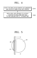
- FIG. 4 is a flowchart of a recrystallizing process in the method of producing the monocrystalline graphene layer, according to an embodiment of the present invention
- FIGS. 5 and 6 are sequential plan views for describing the recrystallizing process in the method of producing the monocrystalline graphene layer, according to an embodiment of the present invention.
- the recrystallizing of the polycrystalline graphene 20 into the monocrystalline graphene 40 by heat-treating the polycrystalline graphene 20 and the catalyst 30 may include heating a first part A1 of a sample 50 including the polycrystalline graphene 20 and the catalyst 30, using a local heater 60 (S310), and moving the local heater 60 to another location to cool the first part A1 and to heat a second part A2 of the sample 50 (S320).
- the heat-treating may be performed by moving the local heater 60 in a direction from a side to another side of the substrate 10 included in the sample 50 (e.g., in a direction from a left side to a right side of FIGS. 5 and 6 ).
- the second part A2 may be a part adjacent to the first part A1 in the direction in which the local heater 60 moves from the first part A1.
- the present invention does not disclose a method of directly growing monocrystalline graphene using a hydrocarbon gas, but discloses a multistage method of growing polycrystalline graphene on a substrate using a hydrocarbon gas, forming a catalyst on the polycrystalline graphene, and then recrystallizing the polycrystalline graphene into monocrystalline graphene by heat-treating the polycrystalline graphene and the catalyst using a zone heating scheme.
- the heat-treating may be understood as post annealing.
- a temperature for producing bulk graphite is equal to or greater than about 2500K in consideration of the size of carbon atoms and bonding between carbon atoms.
- a monolayer has a larger space in which carbon atoms move, and thus a temperature for producing the same may be lower than 2500K.
- different grains should be re-boned to be oriented in a direction, and thus a temperature for producing the same may be in a range of about 1400K to 2000K.
- a metal substrate including, for example, tungsten (W) or molybdenum (Mo) having a high melting point should be used.
- graphene may be grown using a ceramic substrate capable of growing a thin layer at high temperature (e.g., an insulating substrate including Al 2 O 3 , AIN, Si 3 N 4 , SrTiO 3 , or BN).
- a semiconductor device or an electronic device may be manufactured without transferring the grown graphene to another substrate.
- reaction energy may be lowered by utilizing catalyst reaction using organic and inorganic materials to reduce the temperature of recrystallization.
- the present inventor has found that the process temperature may be lowered to 1800K or below if Al or a 3d transition metal compound is used as a catalyst.
- efficient recrystallization may be achieved not by increasing the temperature of a whole sample at once but by moving a heater to increase the temperature of a part of the sample and then scanning the temperature-increased part in a direction.
- recrystallization is induced not by heating the whole sample but by performing a zone heating process to heat an edge of a substrate and then to move a heater in a direction, and thus graphene monocrystalline is grown on the insulating substrate or the composite substrate.
Landscapes
- Chemical & Material Sciences (AREA)
- Organic Chemistry (AREA)
- Engineering & Computer Science (AREA)
- Materials Engineering (AREA)
- Inorganic Chemistry (AREA)
- Metallurgy (AREA)
- Nanotechnology (AREA)
- Crystallography & Structural Chemistry (AREA)
- General Chemical & Material Sciences (AREA)
- Chemical Kinetics & Catalysis (AREA)
- Mechanical Engineering (AREA)
- Physics & Mathematics (AREA)
- Thermal Sciences (AREA)
- Carbon And Carbon Compounds (AREA)
- Crystals, And After-Treatments Of Crystals (AREA)
- Catalysts (AREA)
Abstract
Description
- The present invention relates to a method of producing graphene and, more particularly, to a method of producing monocrystalline graphene.
- Graphene refers to a two-dimensional thin layer with honeycomb structure, comprising one or more layers of carbon atoms. When the carbon atoms are chemically bonded due to an sp2 hybrid orbital, a two-dimensional plane of a hexagonal carbon mesh is provided. Carbon has four outermost electrons, and the four electrons are hybridized to participate in bonding. A method of bonding carbon atoms includes sp3 bonding and sp2 bonding. Carbon atoms bonded using only sp3 bonding correspond to a diamond having a square shape, and carbon atoms bonded using only sp2 bonding correspond to graphite or graphene, a layer of graphite. For example, electrons which should be present in an s orbital and a p orbital have an sp2 or sp3 hybrid orbital corresponding to a combination of the s and p orbitals. The sp2 hybrid orbital has one electron in the s orbital and two electrons in the p orbital, and thus has a total of three electrons. In this case, the electrons have equal energy levels. Having the hybrid orbital is more stable compared to separately having the s and p orbitals. An aggregate of carbon atoms having a planar structure due to sp2 bonding is graphene, and the thickness of a monolayer thereof corresponds to the size of one carbon atom, e.g., about 0.3nm. Graphene has properties of metal. For example, graphene has conductivity in a layer direction, has excellent thermal conductivity, and has a high mobility of charge carriers, and thus may be used to implement a high-speed electronic device. It is known that electron mobility of a graphene sheet has a value of about 20,000 to 50,000 cm2/Vs.
- Since a research group of the University of Manchester, UK has published a method of producing a thin carbon layer having a thickness of one atom, from graphite in 2005, graphene has become one of the most attractive study items in physics because research can be conducted on the unique quantum-Hall effect of graphene and conventionally impossible particle physics experiments can be indirectly implemented using graphene based on a fact that electrons have no effective mass in graphene and thus behave as relativistic particles moving at 1,000 km per sec. (1/300 of the speed of light).
- Using a conventional silicon-based semiconductor process technology, a highly-integrated semiconductor device having a thickness equal to or less than 30 nm may not be easily manufactured because atoms of metal, e.g., gold (Au) or aluminum (Al), deposited on a substrate are thermodynamically unstable, stuck to each other, and thus incapable of obtaining a uniform thin layer if the thickness of the layer thereof is equal to or less than 30 nm, and because the density of impurities doped on silicon is not uniform at the above-mentioned nano-size. However, graphene has a possibility of solving the restriction in integration of the silicon-based semiconductor device technology. Graphene has properties of metal, has a thickness equal to or less than several nm corresponding to an electron shielding thickness, and thus has an electric resistance which varies due to a charge density changed depending on a gate voltage. Using the above characteristics, a metal transistor may be implemented. Furthermore, due to a high mobility of charge carriers, a high-speed electronic device may be implemented. In addition, charges of the charge carriers may be changed from electrons to holes depending on the polarity of the gate voltage, and application to a variety of fields may be expected.
- Currently, a method of obtaining graphene is classified into the following three.
- The first method is a micro cleavage method using cellophane tape. This method has been developed by a research team of the University of Manchester, UK, and researchers use this method due to simplicity thereof. In this method, the thickness of graphite may be reduced by repeatedly peeling graphite using cellophane tape, and a thin graphite layer obtained as described above is transferred onto a substrate. Alternatively, a thin graphite layer is obtained by rubbing graphite on a substrate like rubbing chalk on a blackboard. However, this method depends on the quality of the adhesive tape, and electrodes may not be easily patterned using electron-beam lithography due to a large number of useless and thick graphite particles.
- The second method is a method of epitaxially growing graphene by pyrolyzing silicon carbide (SiC) under high vacuum. This epitaxial growth method is a method of producing graphene using carbon atoms remaining on the surface of SiC after silicon is sublimated from the surface at high vacuum and high temperature, e.g., in a molecular beam epitaxy (MBE) system. In this technology, SiC should be used as a substrate. However, this substrate does not have good performance to be used as an electronic material.
- The third method is a method using chemical peeling of a graphite compound. However, in this method, only a piece of graphite having a thickness of several hundred nanometers may be obtained and graphene may not be obtained. In addition, a chemical material inserted between graphite layers may not be completely removed and thus a large number of defects may be caused.
- The fourth method is a method of growing graphene on a metal substrate using chemical vapor deposition (CVD). However, in this method, graphene may not be oriented in a direction due to growth characteristics thereof. The largest obstacle to commercialization of graphene electronic devices is not a fact that a bandgap may not be easily provided due to material characteristics and thus a logic circuit may not be easily configured, but is a fact that a large-area single crystal, e.g., silicon, may not be easily found. It is currently known that initial uniformity of a graphene layer is controllable by growing graphene on almost melted liquid-state copper. However, even in this case, directivities are not equal and thus growing of a large-area graphene single crystal is impossible. A new idea for producing monocrystalline graphene is required to newly develop electronic devices using graphene.
- The present invention provides a method of growing a graphene layer oriented in a direction, e.g., a monocrystalline graphene layer, on a wafer-scale insulating substrate. However, the scope of the present invention is not limited thereto.
- According to an aspect of the present invention, there is provided a method of manufacturing monocrystalline graphene, the method including forming polycrystalline graphene on a substrate using a hydrocarbon gas, forming a catalyst on the polycrystalline graphene, and recrystallizing the polycrystalline graphene into monocrystalline graphene by heat-treating the polycrystalline graphene and the catalyst.
- The substrate may be an insulating substrate including Al2O3, AIN, Si3N4, SrTiO3, or BN. Alternatively, the substrate may be a composite substrate obtained by growing a transition metal including copper (Cu) or nickel (Ni) in a form of a thin layer having a thickness of 0.5µm to 3µm, on the insulating substrate. The monocrystalline graphene may include monocrystalline graphene grown on the substrate.
- The substrate may be a metal substrate including tungsten (W) or molybdenum (Mo).
- The substrate may include a wafer-scale substrate.
- The forming of the polycrystalline graphene on the substrate using the hydrocarbon gas may be performed at a temperature of 600°C to 1100°C.
- The catalyst may include aluminum (Al), an Al-containing compound, or a 3d transition metal compound.
- The recrystallizing of the polycrystalline graphene into the monocrystalline graphene by heat-treating the polycrystalline graphene and the catalyst may be performed at a temperature of 1400°C to 2000°C.
- The heat-treating may include heating a first part of the polycrystalline graphene and the catalyst using a local heat soruce, and moving the local heat source to another location to cool the first part and to heat a second part at the same time. The heat-treating may be performed by moving the local heater in a direction from one side to the other side of the substrate.
- According to an embodiment of the present invention, a method of growing a graphene layer oriented in a direction, e.g., a monocrystalline graphene layer, on a wafer-scale insulating substrate may be provided. According to an embodiment of the present invention, by growing a graphene layer oriented in a direction, e.g., a monocrystalline graphene layer, on a wafer-scale insulator, graphene electronic devices may be commercialized and thus may lead the post-silicon era. However, the scope of the present invention is not limited to the above-described effect.
-
-
FIG. 1 is a flowchart of a method of producing a monocrystalline graphene layer, according to an embodiment of the present invention. -
FIGS. 2 and 3 are sequential cross-sectional views for describing the method of producing the monocrystalline graphene layer, according to an embodiment of the present invention. -
FIG. 4 is a flowchart of a recrystallizing process in the method of producing the monocrystalline graphene layer, according to an embodiment of the present invention. -
FIGS. 5 and6 are sequential plan views for describing the recrystallizing process in the method of producing the monocrystalline graphene layer, according to an embodiment of the present invention. - Hereinafter, the present invention will be described in detail by explaining embodiments of the invention with reference to the attached drawings. The invention may, however, be embodied in many different forms and should not be construed as being limited to the embodiments set forth herein; rather, these embodiments are provided so that this disclosure will be thorough and complete, and will fully convey the concept of the invention to one of ordinary skill in the art. In the drawings, the sizes of elements are exaggerated for convenience of explanation.
-
FIG. 1 is a flowchart of a method of producing a monocrystalline graphene layer, according to an embodiment of the present invention, andFIGS. 2 and 3 are sequential cross-sectional views for describing the method of producing the monocrystalline graphene layer, according to an embodiment of the present invention. - Referring to
FIGS. 1 to 3 , the method of producing the monocrystalline graphene layer, according to an embodiment of the present invention includes forming polycrystalline graphene 20 on asubstrate 10 using a hydrocarbon gas (S100), forming acatalyst 30 on the polycrystalline graphene 20 (S200), and recrystallizing the polycrystalline graphene 20 intomonocrystalline graphene 40 by heat-treating the polycrystalline graphene 20 and the catalyst 30 (S300). - In the forming of the polycrystalline graphene 20 on the
substrate 10 using the hydrocarbon gas (S100), thesubstrate 10 may be an insulating substrate including Al2O3, AIN, Si3N4, SrTiO3, or BN. Alternatively, thesubstrate 10 may be a composite substrate obtained by growing transition metal including copper (Cu) or nickel (Ni) in the form of a thin layer having a thickness of 0.5µm to 3µm, on an insulator (e.g., an insulating substrate including Al2O3, AIN, Si3N4, SrTiO3, or BN). In this case, themonocrystalline graphene 40 may include monocrystalline graphene grown on the insulating substrate or the composite substrate. In the method of producing the monocrystalline graphene layer, according to a modified embodiment of the present invention, thesubstrate 10 may be a metal substrate including tungsten (W) or molybdenum (Mo). In embodiments of the present invention, thesubstrate 10 may include a wafer-scale substrate. The hydrocarbon gas may include, for example, methyl, methane, ethane, ethylene, acetylene, propane, propylene, butane, butadiene, pentane, or hexane. In the method of producing the monocrystalline graphene layer, according to an embodiment of the present invention, the forming of the polycrystalline graphene 20 on thesubstrate 10 using the hydrocarbon gas (S100) may be performed at a temperature of about 600°C to 1100°C. - In the method of producing the monocrystalline graphene layer, according to an embodiment of the present invention, in the forming of the
catalyst 30 on the polycrystalline graphene 20 (S200), thecatalyst 30 may include aluminum (Al), an Al-containing compound, or a 3d transition metal compound. The 3d transition metal may include, for example, titanium (Ti), vanadium (V), chromium (Cr), manganese (Mn), iron (Fe), cobalt (Co), nickel (Ni), or copper (Cu). For example, the Al-containing compound or the 3d transition metal compound may be Al4C3, KAl2(AlSi3)O10(OH)2, Cu, Ni, Co, Mn, CaO, CrCl2-6H2O, Cr3C2, CrS, CuF2, CuSiF6, CuO, or CuCl. The present inventor has prepared thecatalyst 30 by depositing Al, the Al-containing compound, or the 3d transition metal compound to a very low coverage, or by adsorbing a precursor including the same using chemical vapor deposition (CVD) or atomic layer deposition (ALD), and has found that monocrystalline graphene may be grown on the insulating substrate or the composite substrate using the above-describedcatalyst 30. - In the method of producing the monocrystalline graphene layer, according to an embodiment of the present invention, the recrystallizing of the polycrystalline graphene 20 into the
monocrystalline graphene 40 by heat-treating the polycrystalline graphene 20 and the catalyst 30 (S300) may be performed at a temperature of about 1400°C to 2000°C. The heat-treating may be performed not by increasing the temperature of a whole sample at once but by moving a heater to increase the temperature of a part of the sample and then scanning the temperature-increased part in a direction. A description thereof is now given with reference to the drawings. -
FIG. 4 is a flowchart of a recrystallizing process in the method of producing the monocrystalline graphene layer, according to an embodiment of the present invention, andFIGS. 5 and6 are sequential plan views for describing the recrystallizing process in the method of producing the monocrystalline graphene layer, according to an embodiment of the present invention. - The recrystallizing of the polycrystalline graphene 20 into the
monocrystalline graphene 40 by heat-treating the polycrystalline graphene 20 and the catalyst 30 (S300) may include heating a first part A1 of asample 50 including the polycrystalline graphene 20 and thecatalyst 30, using a local heater 60 (S310), and moving thelocal heater 60 to another location to cool the first part A1 and to heat a second part A2 of the sample 50 (S320). The heat-treating may be performed by moving thelocal heater 60 in a direction from a side to another side of thesubstrate 10 included in the sample 50 (e.g., in a direction from a left side to a right side ofFIGS. 5 and6 ). The second part A2 may be a part adjacent to the first part A1 in the direction in which thelocal heater 60 moves from the first part A1. - The method of producing the monocrystalline graphene layer, according to an embodiment of the present invention has been described above with reference to the drawings.
- The present invention does not disclose a method of directly growing monocrystalline graphene using a hydrocarbon gas, but discloses a multistage method of growing polycrystalline graphene on a substrate using a hydrocarbon gas, forming a catalyst on the polycrystalline graphene, and then recrystallizing the polycrystalline graphene into monocrystalline graphene by heat-treating the polycrystalline graphene and the catalyst using a zone heating scheme. The heat-treating may be understood as post annealing.
- One of factors considered to produce a monocrystalline graphene layer is temperature. A temperature for producing bulk graphite is equal to or greater than about 2500K in consideration of the size of carbon atoms and bonding between carbon atoms. Compared to the bulk, a monolayer has a larger space in which carbon atoms move, and thus a temperature for producing the same may be lower than 2500K. To obtain a single crystal, different grains should be re-boned to be oriented in a direction, and thus a temperature for producing the same may be in a range of about 1400K to 2000K. At this temperature, a metal substrate including, for example, tungsten (W) or molybdenum (Mo) having a high melting point should be used. The solubility of carbon atoms of the metal at this temperature is far apart from the melting point, and thus graphene may be produced due to surface reaction of hydrocarbon. In some embodiments of the present invention, graphene may be grown using a ceramic substrate capable of growing a thin layer at high temperature (e.g., an insulating substrate including Al2O3, AIN, Si3N4, SrTiO3, or BN). In this case, a semiconductor device or an electronic device may be manufactured without transferring the grown graphene to another substrate.
- In the method of producing the monocrystalline graphene layer, according to an embodiment of the present invention, reaction energy may be lowered by utilizing catalyst reaction using organic and inorganic materials to reduce the temperature of recrystallization. The present inventor has found that the process temperature may be lowered to 1800K or below if Al or a 3d transition metal compound is used as a catalyst. The present inventor has also found that efficient recrystallization may be achieved not by increasing the temperature of a whole sample at once but by moving a heater to increase the temperature of a part of the sample and then scanning the temperature-increased part in a direction. That is, recrystallization is induced not by heating the whole sample but by performing a zone heating process to heat an edge of a substrate and then to move a heater in a direction, and thus graphene monocrystalline is grown on the insulating substrate or the composite substrate.
- While the present invention has been particularly shown and described with reference to embodiments thereof, it will be understood by one of ordinary skill in the art that various changes in form and details may be made therein without departing from the spirit and scope of the present invention as defined by the following claims.
Claims (11)
- A method of manufacturing monocrystalline graphene, the method comprising:forming polycrystalline graphene on a substrate using a hydrocarbon gas;forming a catalyst on the polycrystalline graphene; andrecrystallizing the polycrystalline graphene into monocrystalline graphene by heat-treating the polycrystalline graphene and the catalyst.
- The method of claim 1, wherein the substrate is an insulating substrate comprising Al2O3, AIN, Si3N4, SrTiO3, or BN.
- The method of claim 2, wherein the substrate is a composite substrate obtained by growing a transition metal having a thickness of 0.5µm to 3µm, on the insulating substrate.
- The method of claim 2 or 3, wherein the monocrystalline graphene comprises monocrystalline graphene grown on the substrate.
- The method of claim 1, wherein the substrate is a metal substrate comprising tungsten (W) or molybdenum (Mo).
- The method of claim 1, wherein the substrate comprises a wafer-scale substrate.
- The method of claim 1, wherein the forming of the polycrystalline graphene on the substrate using the hydrocarbon gas is performed at a temperature of 600°C to 1100°C.
- The method of claim 1, wherein the catalyst comprises aluminum (Al), an Al-containing compound, or a 3d transition metal compound.
- The method of claim 8, wherein the recrystallizing of the polycrystalline graphene into the monocrystalline graphene by heat-treating the polycrystalline graphene and the catalyst is performed at a temperature of 1400°C to 2000°C.
- The method of claim 1, wherein the heat-treating comprises:heating a first part of the polycrystalline graphene and the catalyst using a local heat source; andmoving the local heat source to another location to cool the first part and to heat a second part at the same time.
- The method of claim 10, wherein the heat-treating is performed by moving the local heat source in a direction from one side to the other side of the substrate.
Applications Claiming Priority (2)
| Application Number | Priority Date | Filing Date | Title |
|---|---|---|---|
| KR1020130167109A KR101572066B1 (en) | 2013-12-30 | 2013-12-30 | Methods of fabricating single crystal graphene |
| PCT/KR2014/012902 WO2015102318A1 (en) | 2013-12-30 | 2014-12-26 | Method for manufacturing monocrystalline graphene |
Publications (3)
| Publication Number | Publication Date |
|---|---|
| EP3091106A1 true EP3091106A1 (en) | 2016-11-09 |
| EP3091106A4 EP3091106A4 (en) | 2017-08-02 |
| EP3091106B1 EP3091106B1 (en) | 2019-02-13 |
Family
ID=53493610
Family Applications (1)
| Application Number | Title | Priority Date | Filing Date |
|---|---|---|---|
| EP14877483.9A Active EP3091106B1 (en) | 2013-12-30 | 2014-12-26 | Method for manufacturing monocrystalline graphene |
Country Status (5)
| Country | Link |
|---|---|
| US (1) | US9834855B2 (en) |
| EP (1) | EP3091106B1 (en) |
| JP (1) | JP2016538236A (en) |
| KR (1) | KR101572066B1 (en) |
| WO (1) | WO2015102318A1 (en) |
Families Citing this family (6)
| Publication number | Priority date | Publication date | Assignee | Title |
|---|---|---|---|---|
| JP6592766B2 (en) * | 2015-07-31 | 2019-10-23 | 川研ファインケミカル株式会社 | Graphene-coated aluminum nitride filler, production method thereof, electronic material, resin composite, and hydrophobic treatment method |
| CN108368469A (en) * | 2015-10-07 | 2018-08-03 | 加利福尼亚大学校董会 | Graphene based multimodal sensor |
| KR102106781B1 (en) * | 2017-11-30 | 2020-05-06 | 성균관대학교산학협력단 | Single-crystal metal thin film and preparing method thereof |
| KR102082694B1 (en) * | 2018-05-09 | 2020-02-28 | 한국과학기술연구원 | Method for directly synthesizing graphene on the surface of target object and device including graphene prepared using the method |
| KR102672480B1 (en) * | 2019-08-30 | 2024-06-07 | 한국전력공사 | Method for preparing doped graphene and doped graphene prepared thereby |
| CN117448969B (en) * | 2023-11-02 | 2025-03-25 | 天津大学 | A kind of ultra-large single crystal domain semiconductor graphene and preparation method thereof |
Family Cites Families (11)
| Publication number | Priority date | Publication date | Assignee | Title |
|---|---|---|---|---|
| JPH06326022A (en) * | 1993-03-16 | 1994-11-25 | Mitsubishi Electric Corp | Semiconductor substrate manufacturing method, semiconductor device manufacturing method, and semiconductor manufacturing apparatus |
| KR101344493B1 (en) * | 2007-12-17 | 2013-12-24 | 삼성전자주식회사 | Single crystalline graphene sheet and process for preparing the same |
| KR101611410B1 (en) * | 2009-04-07 | 2016-04-11 | 삼성전자주식회사 | Manufacturing method of graphene |
| EP2460481A1 (en) * | 2010-12-01 | 2012-06-06 | FACET-LINK Inc. | Fusion implant for facet joints |
| KR20120099917A (en) * | 2011-03-02 | 2012-09-12 | 세종대학교산학협력단 | Method for forming graphene wiring |
| KR101993382B1 (en) * | 2011-05-06 | 2019-06-27 | 삼성전자주식회사 | Graphene on substrate and process for preparing the same |
| KR101878736B1 (en) * | 2011-06-24 | 2018-07-17 | 삼성전자주식회사 | Method for manufacturing graphene |
| KR101165354B1 (en) * | 2011-10-24 | 2012-07-18 | 성균관대학교산학협력단 | Method of manufacturing graphene on the face centered cubic metal catalyst with the single oriented texture |
| US9845551B2 (en) * | 2012-07-10 | 2017-12-19 | William Marsh Rice University | Methods for production of single-crystal graphenes |
| US10053366B2 (en) * | 2012-12-12 | 2018-08-21 | William Marsh Rice Univerisity | Methods of controllably forming bernal-stacked graphene layers |
| US9284640B2 (en) * | 2013-11-01 | 2016-03-15 | Advanced Graphene Products Sp. Z.O.O. | Method of producing graphene from liquid metal |
-
2013
- 2013-12-30 KR KR1020130167109A patent/KR101572066B1/en active Active
-
2014
- 2014-12-26 EP EP14877483.9A patent/EP3091106B1/en active Active
- 2014-12-26 US US15/103,368 patent/US9834855B2/en active Active
- 2014-12-26 WO PCT/KR2014/012902 patent/WO2015102318A1/en not_active Ceased
- 2014-12-26 JP JP2016555437A patent/JP2016538236A/en active Pending
Also Published As
| Publication number | Publication date |
|---|---|
| EP3091106B1 (en) | 2019-02-13 |
| WO2015102318A1 (en) | 2015-07-09 |
| KR20150078047A (en) | 2015-07-08 |
| KR101572066B1 (en) | 2015-11-26 |
| US9834855B2 (en) | 2017-12-05 |
| EP3091106A4 (en) | 2017-08-02 |
| JP2016538236A (en) | 2016-12-08 |
| US20170009371A1 (en) | 2017-01-12 |
Similar Documents
| Publication | Publication Date | Title |
|---|---|---|
| Geng et al. | Recent advances in growth of novel 2D materials: beyond graphene and transition metal dichalcogenides | |
| US9834855B2 (en) | Method for manufacturing monocrystalline graphene | |
| US8632855B2 (en) | Methods of preparing a graphene sheet | |
| Bayer et al. | Atomic-scale in situ observations of crystallization and restructuring processes in two-dimensional MoS2 films | |
| Wang et al. | Direct CVD graphene growth on semiconductors and dielectrics for transfer‐free device fabrication | |
| Dong et al. | Progress in fabrication of transition metal dichalcogenides heterostructure systems | |
| Park et al. | Scanning tunneling microscopy and spectroscopy of air exposure effects on molecular beam epitaxy grown WSe2 monolayers and bilayers | |
| US9040957B2 (en) | Field effect transistor using graphene | |
| CN102392225B (en) | Method for preparing graphene nanoribbon on insulating substrate | |
| US8946692B2 (en) | Graphene (multilayer) boron nitride heteroepitaxy for electronic device applications | |
| US10319589B2 (en) | High performance thin films from solution processible two-dimensional nanoplates | |
| KR101284059B1 (en) | Graphene-Oxide Semiconductor Heterojunction Devices, and Production Method of the Same | |
| Li et al. | Controllable preparation of 2D vertical van der Waals heterostructures and superlattices for functional applications | |
| Niu et al. | Surface Engineering of Two‐Dimensional Materials | |
| EP3356582B1 (en) | Epitaxial growth of defect-free, wafer-scale single-layer graphene on thin films of cobalt | |
| Nakajima et al. | Metal catalysts for layer-exchange growth of multilayer graphene | |
| Kang et al. | Growth of β-SiC nanowires on Si (100) substrates by MOCVD using nickel as a catalyst | |
| Zhao et al. | Epitaxial growth of two-dimensional SnSe 2/MoS 2 misfit heterostructures | |
| Ago et al. | Lattice-oriented catalytic growth of graphene nanoribbons on heteroepitaxial nickel films | |
| Liu et al. | 2D TMD‐Based Lateral Heterostructures: Preparation, Property, and Application | |
| JP2013067549A (en) | Method for forming thin film | |
| JP5872672B2 (en) | Catalyst-free synthesis of vertically aligned CNT on SiNW array | |
| US10840338B2 (en) | Semiconductor device including graphene and method of manufacturing the semiconductor device | |
| CN112689609A (en) | Black phosphorus phase ultrathin bismuth nanosheet modified composite film and preparation method thereof | |
| Sato et al. | Graphene—Novel material for nanoelectronics |
Legal Events
| Date | Code | Title | Description |
|---|---|---|---|
| PUAI | Public reference made under article 153(3) epc to a published international application that has entered the european phase |
Free format text: ORIGINAL CODE: 0009012 |
|
| 17P | Request for examination filed |
Effective date: 20160617 |
|
| AK | Designated contracting states |
Kind code of ref document: A1 Designated state(s): AL AT BE BG CH CY CZ DE DK EE ES FI FR GB GR HR HU IE IS IT LI LT LU LV MC MK MT NL NO PL PT RO RS SE SI SK SM TR |
|
| AX | Request for extension of the european patent |
Extension state: BA ME |
|
| DAX | Request for extension of the european patent (deleted) | ||
| A4 | Supplementary search report drawn up and despatched |
Effective date: 20170629 |
|
| RIC1 | Information provided on ipc code assigned before grant |
Ipc: C01B 32/186 20170101ALI20170623BHEP Ipc: C30B 29/36 20060101ALI20170623BHEP Ipc: C01B 32/196 20170101ALI20170623BHEP Ipc: C30B 25/16 20060101AFI20170623BHEP |
|
| RIC1 | Information provided on ipc code assigned before grant |
Ipc: C01B 32/194 20170101ALI20180412BHEP Ipc: C01B 32/186 20170101ALI20180412BHEP Ipc: C30B 29/36 20060101ALI20180412BHEP Ipc: C01B 32/196 20170101ALI20180412BHEP Ipc: C23C 16/26 20060101ALI20180412BHEP Ipc: C30B 1/08 20060101ALI20180412BHEP Ipc: C30B 25/16 20060101AFI20180412BHEP Ipc: C30B 29/02 20060101ALI20180412BHEP |
|
| GRAP | Despatch of communication of intention to grant a patent |
Free format text: ORIGINAL CODE: EPIDOSNIGR1 |
|
| STAA | Information on the status of an ep patent application or granted ep patent |
Free format text: STATUS: GRANT OF PATENT IS INTENDED |
|
| GRAJ | Information related to disapproval of communication of intention to grant by the applicant or resumption of examination proceedings by the epo deleted |
Free format text: ORIGINAL CODE: EPIDOSDIGR1 |
|
| GRAP | Despatch of communication of intention to grant a patent |
Free format text: ORIGINAL CODE: EPIDOSNIGR1 |
|
| GRAJ | Information related to disapproval of communication of intention to grant by the applicant or resumption of examination proceedings by the epo deleted |
Free format text: ORIGINAL CODE: EPIDOSDIGR1 |
|
| INTG | Intention to grant announced |
Effective date: 20180625 |
|
| GRAP | Despatch of communication of intention to grant a patent |
Free format text: ORIGINAL CODE: EPIDOSNIGR1 |
|
| INTG | Intention to grant announced |
Effective date: 20180706 |
|
| INTG | Intention to grant announced |
Effective date: 20180801 |
|
| GRAS | Grant fee paid |
Free format text: ORIGINAL CODE: EPIDOSNIGR3 |
|
| GRAA | (expected) grant |
Free format text: ORIGINAL CODE: 0009210 |
|
| STAA | Information on the status of an ep patent application or granted ep patent |
Free format text: STATUS: THE PATENT HAS BEEN GRANTED |
|
| AK | Designated contracting states |
Kind code of ref document: B1 Designated state(s): AL AT BE BG CH CY CZ DE DK EE ES FI FR GB GR HR HU IE IS IT LI LT LU LV MC MK MT NL NO PL PT RO RS SE SI SK SM TR |
|
| REG | Reference to a national code |
Ref country code: GB Ref legal event code: FG4D |
|
| REG | Reference to a national code |
Ref country code: CH Ref legal event code: EP Ref country code: AT Ref legal event code: REF Ref document number: 1096294 Country of ref document: AT Kind code of ref document: T Effective date: 20190215 |
|
| REG | Reference to a national code |
Ref country code: IE Ref legal event code: FG4D |
|
| REG | Reference to a national code |
Ref country code: DE Ref legal event code: R096 Ref document number: 602014041113 Country of ref document: DE |
|
| REG | Reference to a national code |
Ref country code: LT Ref legal event code: MG4D |
|
| REG | Reference to a national code |
Ref country code: NL Ref legal event code: MP Effective date: 20190213 |
|
| PG25 | Lapsed in a contracting state [announced via postgrant information from national office to epo] |
Ref country code: NO Free format text: LAPSE BECAUSE OF FAILURE TO SUBMIT A TRANSLATION OF THE DESCRIPTION OR TO PAY THE FEE WITHIN THE PRESCRIBED TIME-LIMIT Effective date: 20190513 Ref country code: FI Free format text: LAPSE BECAUSE OF FAILURE TO SUBMIT A TRANSLATION OF THE DESCRIPTION OR TO PAY THE FEE WITHIN THE PRESCRIBED TIME-LIMIT Effective date: 20190213 Ref country code: PT Free format text: LAPSE BECAUSE OF FAILURE TO SUBMIT A TRANSLATION OF THE DESCRIPTION OR TO PAY THE FEE WITHIN THE PRESCRIBED TIME-LIMIT Effective date: 20190613 Ref country code: SE Free format text: LAPSE BECAUSE OF FAILURE TO SUBMIT A TRANSLATION OF THE DESCRIPTION OR TO PAY THE FEE WITHIN THE PRESCRIBED TIME-LIMIT Effective date: 20190213 Ref country code: NL Free format text: LAPSE BECAUSE OF FAILURE TO SUBMIT A TRANSLATION OF THE DESCRIPTION OR TO PAY THE FEE WITHIN THE PRESCRIBED TIME-LIMIT Effective date: 20190213 Ref country code: LT Free format text: LAPSE BECAUSE OF FAILURE TO SUBMIT A TRANSLATION OF THE DESCRIPTION OR TO PAY THE FEE WITHIN THE PRESCRIBED TIME-LIMIT Effective date: 20190213 |
|
| PG25 | Lapsed in a contracting state [announced via postgrant information from national office to epo] |
Ref country code: LV Free format text: LAPSE BECAUSE OF FAILURE TO SUBMIT A TRANSLATION OF THE DESCRIPTION OR TO PAY THE FEE WITHIN THE PRESCRIBED TIME-LIMIT Effective date: 20190213 Ref country code: GR Free format text: LAPSE BECAUSE OF FAILURE TO SUBMIT A TRANSLATION OF THE DESCRIPTION OR TO PAY THE FEE WITHIN THE PRESCRIBED TIME-LIMIT Effective date: 20190514 Ref country code: HR Free format text: LAPSE BECAUSE OF FAILURE TO SUBMIT A TRANSLATION OF THE DESCRIPTION OR TO PAY THE FEE WITHIN THE PRESCRIBED TIME-LIMIT Effective date: 20190213 Ref country code: BG Free format text: LAPSE BECAUSE OF FAILURE TO SUBMIT A TRANSLATION OF THE DESCRIPTION OR TO PAY THE FEE WITHIN THE PRESCRIBED TIME-LIMIT Effective date: 20190513 Ref country code: IS Free format text: LAPSE BECAUSE OF FAILURE TO SUBMIT A TRANSLATION OF THE DESCRIPTION OR TO PAY THE FEE WITHIN THE PRESCRIBED TIME-LIMIT Effective date: 20190613 Ref country code: RS Free format text: LAPSE BECAUSE OF FAILURE TO SUBMIT A TRANSLATION OF THE DESCRIPTION OR TO PAY THE FEE WITHIN THE PRESCRIBED TIME-LIMIT Effective date: 20190213 |
|
| REG | Reference to a national code |
Ref country code: AT Ref legal event code: MK05 Ref document number: 1096294 Country of ref document: AT Kind code of ref document: T Effective date: 20190213 |
|
| PG25 | Lapsed in a contracting state [announced via postgrant information from national office to epo] |
Ref country code: DK Free format text: LAPSE BECAUSE OF FAILURE TO SUBMIT A TRANSLATION OF THE DESCRIPTION OR TO PAY THE FEE WITHIN THE PRESCRIBED TIME-LIMIT Effective date: 20190213 Ref country code: EE Free format text: LAPSE BECAUSE OF FAILURE TO SUBMIT A TRANSLATION OF THE DESCRIPTION OR TO PAY THE FEE WITHIN THE PRESCRIBED TIME-LIMIT Effective date: 20190213 Ref country code: ES Free format text: LAPSE BECAUSE OF FAILURE TO SUBMIT A TRANSLATION OF THE DESCRIPTION OR TO PAY THE FEE WITHIN THE PRESCRIBED TIME-LIMIT Effective date: 20190213 Ref country code: CZ Free format text: LAPSE BECAUSE OF FAILURE TO SUBMIT A TRANSLATION OF THE DESCRIPTION OR TO PAY THE FEE WITHIN THE PRESCRIBED TIME-LIMIT Effective date: 20190213 Ref country code: IT Free format text: LAPSE BECAUSE OF FAILURE TO SUBMIT A TRANSLATION OF THE DESCRIPTION OR TO PAY THE FEE WITHIN THE PRESCRIBED TIME-LIMIT Effective date: 20190213 Ref country code: RO Free format text: LAPSE BECAUSE OF FAILURE TO SUBMIT A TRANSLATION OF THE DESCRIPTION OR TO PAY THE FEE WITHIN THE PRESCRIBED TIME-LIMIT Effective date: 20190213 Ref country code: AL Free format text: LAPSE BECAUSE OF FAILURE TO SUBMIT A TRANSLATION OF THE DESCRIPTION OR TO PAY THE FEE WITHIN THE PRESCRIBED TIME-LIMIT Effective date: 20190213 Ref country code: SK Free format text: LAPSE BECAUSE OF FAILURE TO SUBMIT A TRANSLATION OF THE DESCRIPTION OR TO PAY THE FEE WITHIN THE PRESCRIBED TIME-LIMIT Effective date: 20190213 |
|
| REG | Reference to a national code |
Ref country code: DE Ref legal event code: R097 Ref document number: 602014041113 Country of ref document: DE |
|
| PG25 | Lapsed in a contracting state [announced via postgrant information from national office to epo] |
Ref country code: PL Free format text: LAPSE BECAUSE OF FAILURE TO SUBMIT A TRANSLATION OF THE DESCRIPTION OR TO PAY THE FEE WITHIN THE PRESCRIBED TIME-LIMIT Effective date: 20190213 Ref country code: SM Free format text: LAPSE BECAUSE OF FAILURE TO SUBMIT A TRANSLATION OF THE DESCRIPTION OR TO PAY THE FEE WITHIN THE PRESCRIBED TIME-LIMIT Effective date: 20190213 |
|
| PLBE | No opposition filed within time limit |
Free format text: ORIGINAL CODE: 0009261 |
|
| STAA | Information on the status of an ep patent application or granted ep patent |
Free format text: STATUS: NO OPPOSITION FILED WITHIN TIME LIMIT |
|
| PG25 | Lapsed in a contracting state [announced via postgrant information from national office to epo] |
Ref country code: AT Free format text: LAPSE BECAUSE OF FAILURE TO SUBMIT A TRANSLATION OF THE DESCRIPTION OR TO PAY THE FEE WITHIN THE PRESCRIBED TIME-LIMIT Effective date: 20190213 |
|
| 26N | No opposition filed |
Effective date: 20191114 |
|
| PG25 | Lapsed in a contracting state [announced via postgrant information from national office to epo] |
Ref country code: SI Free format text: LAPSE BECAUSE OF FAILURE TO SUBMIT A TRANSLATION OF THE DESCRIPTION OR TO PAY THE FEE WITHIN THE PRESCRIBED TIME-LIMIT Effective date: 20190213 |
|
| PG25 | Lapsed in a contracting state [announced via postgrant information from national office to epo] |
Ref country code: TR Free format text: LAPSE BECAUSE OF FAILURE TO SUBMIT A TRANSLATION OF THE DESCRIPTION OR TO PAY THE FEE WITHIN THE PRESCRIBED TIME-LIMIT Effective date: 20190213 |
|
| REG | Reference to a national code |
Ref country code: CH Ref legal event code: PL |
|
| REG | Reference to a national code |
Ref country code: BE Ref legal event code: MM Effective date: 20191231 |
|
| PG25 | Lapsed in a contracting state [announced via postgrant information from national office to epo] |
Ref country code: MC Free format text: LAPSE BECAUSE OF FAILURE TO SUBMIT A TRANSLATION OF THE DESCRIPTION OR TO PAY THE FEE WITHIN THE PRESCRIBED TIME-LIMIT Effective date: 20190213 |
|
| PG25 | Lapsed in a contracting state [announced via postgrant information from national office to epo] |
Ref country code: IE Free format text: LAPSE BECAUSE OF NON-PAYMENT OF DUE FEES Effective date: 20191226 Ref country code: LU Free format text: LAPSE BECAUSE OF NON-PAYMENT OF DUE FEES Effective date: 20191226 |
|
| PG25 | Lapsed in a contracting state [announced via postgrant information from national office to epo] |
Ref country code: LI Free format text: LAPSE BECAUSE OF NON-PAYMENT OF DUE FEES Effective date: 20191231 Ref country code: CH Free format text: LAPSE BECAUSE OF NON-PAYMENT OF DUE FEES Effective date: 20191231 Ref country code: BE Free format text: LAPSE BECAUSE OF NON-PAYMENT OF DUE FEES Effective date: 20191231 |
|
| PG25 | Lapsed in a contracting state [announced via postgrant information from national office to epo] |
Ref country code: CY Free format text: LAPSE BECAUSE OF FAILURE TO SUBMIT A TRANSLATION OF THE DESCRIPTION OR TO PAY THE FEE WITHIN THE PRESCRIBED TIME-LIMIT Effective date: 20190213 |
|
| PG25 | Lapsed in a contracting state [announced via postgrant information from national office to epo] |
Ref country code: HU Free format text: LAPSE BECAUSE OF FAILURE TO SUBMIT A TRANSLATION OF THE DESCRIPTION OR TO PAY THE FEE WITHIN THE PRESCRIBED TIME-LIMIT; INVALID AB INITIO Effective date: 20141226 Ref country code: MT Free format text: LAPSE BECAUSE OF FAILURE TO SUBMIT A TRANSLATION OF THE DESCRIPTION OR TO PAY THE FEE WITHIN THE PRESCRIBED TIME-LIMIT Effective date: 20190213 |
|
| PG25 | Lapsed in a contracting state [announced via postgrant information from national office to epo] |
Ref country code: MK Free format text: LAPSE BECAUSE OF FAILURE TO SUBMIT A TRANSLATION OF THE DESCRIPTION OR TO PAY THE FEE WITHIN THE PRESCRIBED TIME-LIMIT Effective date: 20190213 |
|
| PGFP | Annual fee paid to national office [announced via postgrant information from national office to epo] |
Ref country code: FR Payment date: 20250925 Year of fee payment: 12 |
|
| PGFP | Annual fee paid to national office [announced via postgrant information from national office to epo] |
Ref country code: DE Payment date: 20250922 Year of fee payment: 12 |
|
| PGFP | Annual fee paid to national office [announced via postgrant information from national office to epo] |
Ref country code: GB Payment date: 20251001 Year of fee payment: 12 |