EP3089556A1 - Illumination lamp, illumination apparatus, and illumination control circuit - Google Patents
Illumination lamp, illumination apparatus, and illumination control circuit Download PDFInfo
- Publication number
- EP3089556A1 EP3089556A1 EP16167287.8A EP16167287A EP3089556A1 EP 3089556 A1 EP3089556 A1 EP 3089556A1 EP 16167287 A EP16167287 A EP 16167287A EP 3089556 A1 EP3089556 A1 EP 3089556A1
- Authority
- EP
- European Patent Office
- Prior art keywords
- voltage
- illumination lamp
- illumination
- ballast
- fluorescent lamps
- Prior art date
- Legal status (The legal status is an assumption and is not a legal conclusion. Google has not performed a legal analysis and makes no representation as to the accuracy of the status listed.)
- Granted
Links
- 238000005286 illumination Methods 0.000 title claims abstract description 113
- 230000007704 transition Effects 0.000 claims description 7
- 230000007423 decrease Effects 0.000 claims description 3
- 238000001514 detection method Methods 0.000 description 20
- 239000000758 substrate Substances 0.000 description 10
- 239000003990 capacitor Substances 0.000 description 6
- 238000000034 method Methods 0.000 description 4
- 230000008901 benefit Effects 0.000 description 2
- 238000009499 grossing Methods 0.000 description 2
- 238000012986 modification Methods 0.000 description 2
- 230000004048 modification Effects 0.000 description 2
- 238000011084 recovery Methods 0.000 description 2
- 239000004065 semiconductor Substances 0.000 description 2
- XUIMIQQOPSSXEZ-UHFFFAOYSA-N Silicon Chemical compound [Si] XUIMIQQOPSSXEZ-UHFFFAOYSA-N 0.000 description 1
- 239000011521 glass Substances 0.000 description 1
- 239000011347 resin Substances 0.000 description 1
- 229920005989 resin Polymers 0.000 description 1
- 229910052710 silicon Inorganic materials 0.000 description 1
- 239000010703 silicon Substances 0.000 description 1
Images



Classifications
-
- H—ELECTRICITY
- H05—ELECTRIC TECHNIQUES NOT OTHERWISE PROVIDED FOR
- H05B—ELECTRIC HEATING; ELECTRIC LIGHT SOURCES NOT OTHERWISE PROVIDED FOR; CIRCUIT ARRANGEMENTS FOR ELECTRIC LIGHT SOURCES, IN GENERAL
- H05B45/00—Circuit arrangements for operating light-emitting diodes [LED]
- H05B45/40—Details of LED load circuits
-
- F—MECHANICAL ENGINEERING; LIGHTING; HEATING; WEAPONS; BLASTING
- F21—LIGHTING
- F21K—NON-ELECTRIC LIGHT SOURCES USING LUMINESCENCE; LIGHT SOURCES USING ELECTROCHEMILUMINESCENCE; LIGHT SOURCES USING CHARGES OF COMBUSTIBLE MATERIAL; LIGHT SOURCES USING SEMICONDUCTOR DEVICES AS LIGHT-GENERATING ELEMENTS; LIGHT SOURCES NOT OTHERWISE PROVIDED FOR
- F21K9/00—Light sources using semiconductor devices as light-generating elements, e.g. using light-emitting diodes [LED] or lasers
- F21K9/20—Light sources comprising attachment means
- F21K9/27—Retrofit light sources for lighting devices with two fittings for each light source, e.g. for substitution of fluorescent tubes
-
- F—MECHANICAL ENGINEERING; LIGHTING; HEATING; WEAPONS; BLASTING
- F21—LIGHTING
- F21Y—INDEXING SCHEME ASSOCIATED WITH SUBCLASSES F21K, F21L, F21S and F21V, RELATING TO THE FORM OR THE KIND OF THE LIGHT SOURCES OR OF THE COLOUR OF THE LIGHT EMITTED
- F21Y2115/00—Light-generating elements of semiconductor light sources
- F21Y2115/10—Light-emitting diodes [LED]
-
- Y—GENERAL TAGGING OF NEW TECHNOLOGICAL DEVELOPMENTS; GENERAL TAGGING OF CROSS-SECTIONAL TECHNOLOGIES SPANNING OVER SEVERAL SECTIONS OF THE IPC; TECHNICAL SUBJECTS COVERED BY FORMER USPC CROSS-REFERENCE ART COLLECTIONS [XRACs] AND DIGESTS
- Y02—TECHNOLOGIES OR APPLICATIONS FOR MITIGATION OR ADAPTATION AGAINST CLIMATE CHANGE
- Y02B—CLIMATE CHANGE MITIGATION TECHNOLOGIES RELATED TO BUILDINGS, e.g. HOUSING, HOUSE APPLIANCES OR RELATED END-USER APPLICATIONS
- Y02B20/00—Energy efficient lighting technologies, e.g. halogen lamps or gas discharge lamps
- Y02B20/30—Semiconductor lamps, e.g. solid state lamps [SSL] light emitting diodes [LED] or organic LED [OLED]
Definitions
- the present invention relates to an illumination lamp, an illumination apparatus, and an illumination control circuit.
- LED illumination lamp having an output of an inverter ballast for fluorescent lamps as an input, is one of such illumination lamps and can be used in replacing a conventional fluorescent lamp.
- inverter ballast for fluorescent lamps which performs an anomaly detection at the startup, and does not allow a fluorescent lamp to be turned on by performing a protection operation when an anomaly is detected.
- an LED illumination lamp is attached, replacing the fluorescent lamp, to the above described inverter ballast for fluorescent lamps, there may be a case where the LED illumination lamp is not turned on due to the protection operation.
- the above case may be considered as follows.
- a fluorescent lamp When a fluorescent lamp is used, current does not flow in the fluorescent lamp at the startup; but when an LED illumination is used, there is a case where current flows in the LED illumination lamp at the startup, an anomaly is detected by the inverter ballast for fluorescent lamps, and the protection operation is performed. Therefore, in order to connect an LED illumination lamp to an inverter ballast for fluorescent lamps, the above problem needs to be resolved.
- a technique which includes a full-wave rectifier circuit for rectifying a high frequency from the inverter ballast; a smoothing capacitor connected to the full-wave rectifier circuit via an inductor element; and an LED unit connected to the smoothing capacitor.
- the technique includes setting an impedance of the inductor element to be a value sufficient for twice the high frequency from the inverter ballast for fluorescent lamps.
- the inverter ballast for fluorescent lamps continues outputting a high voltage even after the inverter ballast for fluorescent lamps transitions to a stable operation, and thus, energy saving cannot be realized.
- Patent Document 1 Japanese Laid-Open Patent Application No. 11-135274
- An illumination lamp connectable to an inverter ballast for fluorescent lamps includes a light emitting diode; a rectifier circuit configured to rectify an AC voltage supplied by the inverter ballast for fluorescent lamps and supply the rectified voltage to the light emitting diode; and a switching circuit configured to be in a non-conductive state when the rectified voltage from the rectifier circuit is less than a predetermined voltage and not allow current to flow in the light emitting diode, to switch to a conductive state when the rectified voltage from the rectifier circuit is equal to or greater than the predetermined voltage and allow the current to flow in the light emitting diode, and to continue in the conductive state even when the rectified voltage changes to be less than the predetermined voltage after switching to the conductive state.
- stable illumination can be provided when an illumination lamp with a light emitting diode is connected to an inverter ballast for fluorescent lamps.
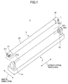
- Fig. 1 is a perspective view illustrating an appearance of an illumination apparatus 1 according to a first embodiment.
- the illumination apparatus 1 includes an illumination lamp 2 and an illumination fixture 5 which removably connects the illumination lamp 2.
- the illumination lamp 2 includes a translucent unit 20 and mouthpieces 21 and 22.
- the translucent unit 20 includes a member made of light-transmissive resin or glass through which light emitted from an embedded light source (an LED module 27 which will be described later) is transmitted, which member is sealed by the mouthpiece 21 disposed at one end and the mouthpiece 22 disposed at the other end.
- the translucent unit 20 may be, for example, straight tubular.
- the mouthpiece 21 includes convex terminals 211 and 212.
- the mouthpiece 22 includes convex terminals 221 and 222. Some of the terminals, however, are not shown in Fig. 1 (refer to Fig. 9 which will be described later). It should be noted that an electric circuit is disposed in the translucent unit 20 (refer to Fig. 3 which will be described later).
- the illumination fixture 5 includes a fluorescent ballast 50 (refer to Fig. 9 ), sockets 51 and 52 to which the illumination lamp 2 can be removably attached, and is connectable to commercial AC power.
- the commercial AC power frequency is, for example, 50 Hz or 60 Hz.
- the commercial AC power is supplied to the fluorescent ballast 50.
- the fluorescent ballast 50 may be, for example, a well-known fluorescent glow ballast, a fluorescent rapid ballast, an inverter ballast for fluorescent lamps, or the like.
- the illumination lamp 2 may be, however, directly connectable to the commercial AC power, and, in this case, the fluorescent ballast 50 is not needed. In this way, the illumination lamp 2 may be connectable to any one of the fluorescent glow ballast, the fluorescent rapid ballast, the inverter ballast for fluorescent lamps and the commercial AC power.
- the socket 51 includes concave terminals 511 and 512.
- the socket 52 includes concave terminals 521 and 522. Some of the terminals, however, are not shown in Fig. 1 (refer to Fig. 9 which will be described later).
- the terminals 211 and 212 of the mouthpiece 21 of the illumination lamp 2 are inserted into, engaged with, and electrically connected to the terminals 511 and 512 of the socket 51 of the illumination fixture 5.
- the terminals 221 and 222 of the mouthpiece 22 of the illumination lamp 2 are inserted into, engaged with, and electrically connected to the terminals 521 and 522 of the socket 52 of the illumination fixture 5.
- Fig. 2 is a cross-section view illustrating an illumination lamp 2 according to the first embodiment.
- a frame 410 is fixed inside the translucent unit 20.
- An LED substrate 420 on which an LED module 27 is mounted is removably installed on one side of the frame 410.
- a holder 430 is disposed on another side of the frame 410.
- a DRV substrate 440 on which rectifier circuits 24 and 25, a drive circuit 26, etc., are mounted is removably installed in the holder 430.
- Cross-sectional shapes of the frame 410 and the holder 430 are substantially the same in the longitudinal direction, and the frame 410 and the holder 430 can be inserted into the translucent unit 20 by sliding them in the longitudinal direction from an end of the translucent unit 20 into inside the translucent unit 20.
- cross-sectional shapes of the LED substrate 420 and the DRV substrate 440 are substantially the same in the longitudinal direction, and the LED substrate 420 and the DRV substrate 440 can be inserted into the translucent unit 20 by sliding them in the longitudinal direction from an end of the translucent unit 20 into inside the translucent unit 20.
- the shape of the illumination lamp 2 is similar to a straight tubular fluorescent lamp and is easily exchangeable with an existing fluorescent lamp attached to the illumination fixture 5.
- the shape of the illumination lamp 2 may not be necessarily similar to the existing fluorescent lamp.
- the cross-sectional shape of the translucent unit 20 may not be circular and may be semicircular, or the like.
- Fig. 3 is a drawing illustrating circuit blocks of an illumination lamp 2 according to the first embodiment.
- the illumination lamp 2 includes as major units the mouthpieces 21 and 22, a filter circuit 23, the rectifier circuits 24 and 25, the drive circuit 26, an LED module 27 and an inverter detection circuit 28.
- the filter circuit 23 is an EMI countermeasure filter which is a circuit for reducing electromagnetic noise emitted by the illumination lamp 2.
- the filter circuit 23 may be a circuit in which, for example, an inter-line capacitor (X-capacitor), a versus-ground capacitor (Y-capacitor), a common mode coil, a normal mode coil, and the like, are connected in series or in parallel.
- the illumination lamp 2 is capable of reducing electromagnetic noise by including the filter circuit 23, and satisfies the EMI (ElectroMagnetic Interference) standards.
- the filter circuit 23 is configured to be by-passed using a switching circuit 61.
- the switching circuit 61 may be configured to include, for example, a relay or a semiconductor switch (e.g., FET).
- the rectifier circuits 24 and 25 are circuits for rectifying AC voltages supplied directly from the mouthpieces 21 and 22, or via the filter circuit 23, and supplying the rectified voltages to the LED module 27 via the drive circuit 26.
- the drive circuit 26 is a circuit for driving the LED module 27 which includes a plurality of light emitting diodes.
- the drive circuit 26 may be configured to include, for example, a buck-boost circuit, a constant current circuit, or the like. By including the drive circuit 26, it becomes possible to supply appropriate current not exceeding the rated current to the LED module 27 even when the voltages supplied from the rectifier circuits 24 and 25 may vary, thereby a failure of the LED module 27 can be avoided and power saving can be achieved.
- the illumination lamp 2 is configured to be connectable to any one of the fluorescent glow ballast, the fluorescent rapid ballast, the inverter ballast for fluorescent lamps and the commercial AC power and capable of selecting circuits for use depending on the connected target.
- the inverter detection circuit 28 is a circuit for detecting whether the fluorescent ballast 50 included in the illumination fixture 5 is an inverter ballast for fluorescent lamps when the illumination lamp 2 is connected to the illumination fixture 5 and powered.
- the frequency of a signal input to the illumination lamp 2 from the fluorescent ballast 50 is a high frequency on the order of several tens KHz.
- the inverter detection circuit 28 can detect whether the fluorescent ballast 50 included in the illumination fixture 5 is an inverter ballast for fluorescent lamps based on, for example, the frequency of a signal input to the illumination lamp 2.
- the filter circuit 23 is by-passed by the switching circuit 61. Further, a switching circuit 33, which will be described later, becomes effective only in a case where it is detected that the fluorescent ballast 50 is an inverter ballast for fluorescent lamps, and is by-passed by the switching circuit 61 in other cases.
- the inverter detection circuit 28 detects that the fluorescent ballast 50 included in the illumination fixture 5 is an inverter ballast for fluorescent lamps
- the signal input to the illumination lamp 2 from the inverter ballast for fluorescent lamps via the mouthpieces 21 and 22 is, by by-passing the filter circuit 23, supplied to the rectifier circuits 24 and 25.
- the outputs of the rectifier circuits 24 and 25 are supplied to the LED module 27 through the switching circuit 33 (the drive circuit 26 is by-passed).
- high frequency filter circuits 63 may be disposed separately from the filter circuit 23. Furthermore, in the case where the inverter detection circuit 28 detects that the fluorescent ballast 50 included in the illumination fixture 5 is an inverter ballast for fluorescent lamps, the outputs of the mouthpieces 21 and 22 may, by using the switching circuit 61, pass through the high frequency filter circuits 63. As a result, even if the filter circuit 23 is by-passed, an EMI noise problem does not occur and it becomes possible to provide appropriate current not exceeding the rated current to the LED module 27. Also, there may be a case where the fluorescent ballast 50 performs a function corresponding to the filter circuits.
- the drive circuit 26 may be capable of being by-passed by a switching circuit.
- the switching circuit may be configured to include, for example, a relay or a semiconductor switch (e.g., FET).
- FET semiconductor switch
- the outputs of the mouthpieces 21 and 22 may, by using the switching circuit 61, pass through the high frequency filter circuits 63.
- second drive circuits 66 may be disposed separately from the drive circuit 26.
- the illumination lamp 2 may be configured to include a rapid detection circuit 29.
- the rapid detection circuit 29 is a circuit for detecting whether the fluorescent ballast 50 included in the illumination fixture 5 is a fluorescent rapid ballast when the illumination lamp 2 is connected to the illumination fixture 5 and powered.
- the filter circuit 23 and the drive circuit 26 may not be by-passed, but the specification of the drive circuit 26 may be changed.
- the inverter detection circuit 28 does not detect that the fluorescent ballast 50 is an inverter ballast for fluorescent lamps and the rapid detection circuit 29 does not detect that the fluorescent ballast 50 is a fluorescent rapid ballast.
- the fluorescent ballast 50 is a fluorescent glow ballast or the illumination lamp 2 is not connected through the fluorescent ballast 50, but directly connected to the commercial AC power, and the signals input to the illumination lamp 2 through the mouthpieces 21 and 22 are supplied to the rectifier circuits 24 and 25 via the filter circuit 23. Then, the outputs of the rectifier circuits 24 and 25 are supplied to the LED module 27 via the drive circuit 26.
- the specification of the drive circuit 26 a specification which fits the fluorescent glow ballast and the commercial AC power may be selected.
- the outputs of the mouthpieces 21 and 22 may, by using the switching circuit 61, pass through the high frequency filter circuits 63.
- the filter circuit 23 and the high frequency filter circuits 63 may not be included.
- FIG. 9 characteristic operations of the illumination lamp 2 will be described. It should be noted that, in Fig. 9 , wire connections only for the major circuits of the illumination lamp 2 according to the embodiment are shown and an illustration of wire connections for portions not related to the characteristic operations is omitted.
- the terminals 211 and 212 of the mouthpiece 21 of the illumination lamp 2 are inserted, engaged with, and electrically connected to the respective terminals 511 and 512 of the socket 51 of the illumination fixture 5.
- the terminals 221 and 222 of the mouthpiece 22 of the illumination lamp 2 are inserted into, engaged with, and electrically connected to the respective terminals 521 and 522 of the socket 52 of the illumination fixture 5.
- the rectifier circuits 24 and 25 are, for example, bridge type full-wave rectifier circuits configured to include a so-called fast recovery diode whose reverse recovery time is short.
- the rectifier circuits 24 and 25 rectify the AC voltages which are input from the mouthpieces 21 and 22 through the filter circuits 23 (not shown in Fig. 9 ).
- a rectified voltage V 1 rectified by the rectifier circuits 24 and 25 is, through the plus side wire connection 31 and the minus side wire connection 32 which are output units of the rectifier circuits 24 and 25, and through the drive circuit 26 (not shown in Fig. 9 ), supplied to the LED module 27.
- the rectifier circuits 24 and 25 rectify the AC voltage directly input from the inverter ballast for fluorescent lamps without passing through the filter circuit 23. Further, the rectified voltage V 1 rectified by the rectifier circuits 24 and 25 is output to the plus side wire connection 31 and the minus side wire connection 32, and, through the switching circuit 33 (the drive circuit 26 is by-passed), supplied to the LED module 27.
- the switching circuit 33 is inserted in the plus side wire connection 31, and is a circuit a state of which is switched between a conductive state and a non-conductive state according to the voltage V 1 (voltage between the plus side wire connection 31 and the minus side wire connection 32) rectified by the rectifier circuits 24 and 25. Specifically, when the voltage V 1 is less than a predetermined voltage, the switching circuit 33 is non-conductive and does not allow the current to flow in the LED module 27. When the voltage V 1 is equal to or more than the predetermined voltage, the switching circuit 33 is conductive and allows the current to flow in the LED module 27; and after the switching circuit 33 become conductive, it keeps being conductive even if the voltage V 1 changes to be less than the predetermined voltage.
- the switching circuit 33 can be by-passed by using the switching circuit 61.
- the switching circuit 33 includes a silicon diode alternating current bi-directional switch (SIDAC (registered trademark)). It should be noted that the switching circuit 33 may include not only a single switching element like a SIDAC but also multiple elements.
- the switching circuit 33 may include a detection unit for detecting the voltage V 1 and a switch unit for switching between a conductive state and a non-conductive state of the plus side wire connection 31.
- the circuit switches to a conductive state when the voltage V 1 is equal to or more than a predetermined voltage, and continues in a conductive state even the voltage V 1 becomes less than the predetermined voltage after the voltage V 1 has become equal to or more than the predetermined voltage.
- a part of the circuit may include an element such as a thyristor or a triode for alternating current (TRIAC).
- the LED module 27 includes a plurality of serial connection units in which a plurality of light emitting diodes 271 are connected in series between the plus side wire connection 31 and the minus side wire connection 32 (6 light emitting diodes 271 are connected in series in Fig. 9 ). Further, the serial connection units are connected in parallel. When the switching circuit 33 switches to a conductive state, current flows in the light emitting diodes 271, and light is emitted.
- the fluorescent ballast 50 is an inverter ballast for fluorescent lamps
- an inverter ballast for fluorescent lamps which performs an anomaly detection at the startup.
- a fluorescent lamp is connected to an inverter ballast for fluorescent lamps
- current does not flow in the fluorescent lamp. Therefore, in the case where an illumination lamp 2 is connected to the inverter ballast for fluorescent lamps, it is necessary to make the same things happen as in the case where a fluorescent lamp is connected to the inverter ballast for fluorescent lamps. If different things happen, the inverter ballast for fluorescent lamps may detect an anomaly, a protection operation may be performed, and the illumination lamp 2 may not be turned on.
- the switching circuit 33 is included. Further, the predetermined voltage with which the switching circuit 33 switches to a conductive state is set greater than a voltage the inverter ballast for fluorescent lamps outputs at the startup, and less than a voltage the inverter ballast for fluorescent lamps outputs when it transitions from the startup operation to the stable operation.
- a SIDAC a breakover voltage of which is 200 V
- the voltage V 1 is less than the SIDAC breakover voltage, 200 V
- current does not flow from the inverter ballast for fluorescent lamps to the rectifier circuits 24 and 25.
- the voltage V 1 is equal to or more than 200 V, current flows from the inverter ballast for fluorescent lamps to the rectifier circuits 24 and 25.
- the voltage V 1 applied by the inverter ballast for fluorescent lamps at the startup is a little less than 200 V at most. Therefore, the current does not flow from the inverter ballast for fluorescent lamps to the rectifier circuits 24 and 25 at the startup, which is the same behavior as in the case where a fluorescent lamp is connected to the inverter ballast for fluorescent lamps. As a result, a problem can be solved in which the illumination lamp 2 is not turned on.
- the voltage V 1 applied by the inverter ballast for fluorescent lamps gradually increases to a little more than 200 V that is the breakover voltage of the SIDAC, and transitions to a stable operation.
- the voltage V 1 is equal to or more than the breakover voltage of the SIDAC, current flows from the inverter ballast for fluorescent lamps to the rectifier circuits 24 and 25, and the current is provided to the LED module 27 through the SIDAC.
- the voltage V 1 applied by the inverter ballast for fluorescent lamps decreases to a voltage in which a voltage-drop voltage at the SIDAC (a little less than 1 V) is added to a sum of the forward voltages of the light emitting diodes 271 included in each of the serial connection units of the LED module 27.
- the switching circuit 33 by using the switching circuit 33, it becomes possible to avoid a situation in which the illumination lamp 2 is not turned on by having an anomaly detected by the anomaly detection performed at the startup of the inverter ballast for fluorescent lamps. In this way, the LED module 27 is capable of providing stable illumination.
- the sum of the forward voltages of the light emitting diodes 271 included in each of the serial connection units of the LED module 27 is set to be a voltage (e.g., about 80 V) less than a voltage normally applied at the stable operation of a fluorescent lamp (a little more than 200 V). Therefore, it becomes possible to make a voltage when the inverter ballast for fluorescent lamps transitions to a stable operation (e.g., 80 V + voltage-drop voltage at the SIDAC) less than a voltage of a case where a fluorescent lamp is used (about a little more than 200 V), and thus, energy saving can be achieved.
- a voltage e.g. 80 V
- a stable operation e.g. 80 V + voltage-drop voltage at the SIDAC
- the breakover voltage be about 200 V.
- the more the breakover voltage decreases from 200 V the more increases the likelihood of the breakover voltage being less than a voltage output by the inverter ballast for fluorescent lamps at the startup, and the protection operation is performed as a result of anomaly detection of the inverter ballast for fluorescent lamps.
- the more the breakover voltage increases above 200 V the more increases the likelihood of the voltage output by the inverter ballast for fluorescent lamps when it transitions from the startup to a stable operation cannot exceed the breakover voltage, and the current is not provided to the illumination lamp 2 and the illumination lamp 2 is not turned on.
- an illumination lamp which is capable of connecting to any one of the fluorescent glow ballast, the fluorescent rapid ballast, the fluorescent inverter ballast and the commercial AC power.
- the present invention can be applied to an illumination lamp capable of being connected to at least an inverter ballast for fluorescent lamps.
- the present invention can be applied to an illumination lamp which can be connected to only the inverter ballast for fluorescent lamps, and also applied to an illumination lamp which can be connected to not only the inverter ballast for fluorescent lamps but also other fluorescent ballasts or the commercial AC power.
- the illumination lamp capable of being connected to only an inverter ballast for fluorescent lamps
- only necessary units in the circuit blocks shown in FIGs. 3 through 8 may be included.
- the inverter detection circuit 28, the rapid detection circuit 29, the filter circuit 23, the drive circuit 26 or the like may not be included.
Landscapes
- Circuit Arrangement For Electric Light Sources In General (AREA)
- Fastening Of Light Sources Or Lamp Holders (AREA)
- Non-Portable Lighting Devices Or Systems Thereof (AREA)
Abstract
Description
- The present invention relates to an illumination lamp, an illumination apparatus, and an illumination control circuit.
- In recent years, illumination lamps using a light emitting diode (LED) (hereinafter also referred to as an LED illumination lamp) with features of low power consumption, long service life, and the like, have been drawing attention. An LED illumination lamp, having an output of an inverter ballast for fluorescent lamps as an input, is one of such illumination lamps and can be used in replacing a conventional fluorescent lamp.
- It should be noted that there is an inverter ballast for fluorescent lamps which performs an anomaly detection at the startup, and does not allow a fluorescent lamp to be turned on by performing a protection operation when an anomaly is detected. When an LED illumination lamp is attached, replacing the fluorescent lamp, to the above described inverter ballast for fluorescent lamps, there may be a case where the LED illumination lamp is not turned on due to the protection operation.
- The above case may be considered as follows. When a fluorescent lamp is used, current does not flow in the fluorescent lamp at the startup; but when an LED illumination is used, there is a case where current flows in the LED illumination lamp at the startup, an anomaly is detected by the inverter ballast for fluorescent lamps, and the protection operation is performed. Therefore, in order to connect an LED illumination lamp to an inverter ballast for fluorescent lamps, the above problem needs to be resolved.
- As an example method for resolving the problem, a technique is known which includes a full-wave rectifier circuit for rectifying a high frequency from the inverter ballast; a smoothing capacitor connected to the full-wave rectifier circuit via an inductor element; and an LED unit connected to the smoothing capacitor. The technique includes setting an impedance of the inductor element to be a value sufficient for twice the high frequency from the inverter ballast for fluorescent lamps.
- However, in the above technique, the inverter ballast for fluorescent lamps continues outputting a high voltage even after the inverter ballast for fluorescent lamps transitions to a stable operation, and thus, energy saving cannot be realized.
- It is an object of the present invention to obviate the above problem, provide stable illumination when an illumination lamp with a light emitting diode is used by being connected to an inverter ballast for fluorescent lamps, and realize the energy saving.
- [Patent Document 1] Japanese Laid-Open Patent Application No.
11-135274 - An illumination lamp connectable to an inverter ballast for fluorescent lamps is provided. The illumination lamp includes a light emitting diode; a rectifier circuit configured to rectify an AC voltage supplied by the inverter ballast for fluorescent lamps and supply the rectified voltage to the light emitting diode; and a switching circuit configured to be in a non-conductive state when the rectified voltage from the rectifier circuit is less than a predetermined voltage and not allow current to flow in the light emitting diode, to switch to a conductive state when the rectified voltage from the rectifier circuit is equal to or greater than the predetermined voltage and allow the current to flow in the light emitting diode, and to continue in the conductive state even when the rectified voltage changes to be less than the predetermined voltage after switching to the conductive state.
- According to the present invention, stable illumination can be provided when an illumination lamp with a light emitting diode is connected to an inverter ballast for fluorescent lamps.
- Other objects, features and advantages of the present invention will become more apparent from the following detailed description when read in conjunction with the accompanying drawings.
-
-
Fig. 1 is a perspective view illustrating an appearance of an illumination apparatus according to a first embodiment. -
Fig. 2 is a cross-sectional view illustrating an illumination lamp according to the first embodiment. -
Fig. 3 is a drawing illustrating circuit blocks of an illumination lamp according to the first embodiment. -
Fig. 4 is a drawing illustrating circuit blocks of an illumination lamp according to a modified example 1 of the first embodiment. -
Fig. 5 is a drawing illustrating circuit blocks of an illumination lamp according to a modified example 2 of the first embodiment. -
Fig. 6 is a drawing illustrating circuit blocks of an illumination lamp according to a modified example 3 of the first embodiment. -
Fig. 7 is a drawing illustrating circuit blocks of an illumination lamp according to a modified example 4 of the first embodiment. -
Fig. 8 is a drawing illustrating circuit blocks of an illumination lamp according to a modified example 5 of the first embodiment. -
Fig. 9 is a drawing illustrating a wire connection of major circuits of an illumination lamp according to the first embodiment. - In the following, embodiments of the present invention will be described referring to the drawings. In each of the drawings, the same numeral is assigned to the same element and a duplicated description may be omitted.
-
Fig. 1 is a perspective view illustrating an appearance of anillumination apparatus 1 according to a first embodiment. Referring toFig. 1 , theillumination apparatus 1 includes anillumination lamp 2 and anillumination fixture 5 which removably connects theillumination lamp 2. - The
illumination lamp 2 includes atranslucent unit 20 andmouthpieces translucent unit 20 includes a member made of light-transmissive resin or glass through which light emitted from an embedded light source (anLED module 27 which will be described later) is transmitted, which member is sealed by themouthpiece 21 disposed at one end and themouthpiece 22 disposed at the other end. Thetranslucent unit 20 may be, for example, straight tubular. - The
mouthpiece 21 includes convexterminals mouthpiece 22 includesconvex terminals Fig. 1 (refer toFig. 9 which will be described later). It should be noted that an electric circuit is disposed in the translucent unit 20 (refer toFig. 3 which will be described later). - The
illumination fixture 5 includes a fluorescent ballast 50 (refer toFig. 9 ),sockets illumination lamp 2 can be removably attached, and is connectable to commercial AC power. The commercial AC power frequency is, for example, 50 Hz or 60 Hz. The commercial AC power is supplied to thefluorescent ballast 50. - The
fluorescent ballast 50 may be, for example, a well-known fluorescent glow ballast, a fluorescent rapid ballast, an inverter ballast for fluorescent lamps, or the like. Theillumination lamp 2 may be, however, directly connectable to the commercial AC power, and, in this case, thefluorescent ballast 50 is not needed. In this way, theillumination lamp 2 may be connectable to any one of the fluorescent glow ballast, the fluorescent rapid ballast, the inverter ballast for fluorescent lamps and the commercial AC power. - The
socket 51 includesconcave terminals socket 52 includesconcave terminals Fig. 1 (refer toFig. 9 which will be described later). - The
terminals mouthpiece 21 of theillumination lamp 2 are inserted into, engaged with, and electrically connected to theterminals socket 51 of theillumination fixture 5. Similarly, theterminals mouthpiece 22 of theillumination lamp 2 are inserted into, engaged with, and electrically connected to theterminals socket 52 of theillumination fixture 5. -
Fig. 2 is a cross-section view illustrating anillumination lamp 2 according to the first embodiment. As shown inFig. 2 , in theillumination lamp 2, aframe 410 is fixed inside thetranslucent unit 20. AnLED substrate 420 on which anLED module 27 is mounted is removably installed on one side of theframe 410. Further, aholder 430 is disposed on another side of theframe 410. ADRV substrate 440 on whichrectifier circuits drive circuit 26, etc., are mounted is removably installed in theholder 430. - Cross-sectional shapes of the
frame 410 and theholder 430 are substantially the same in the longitudinal direction, and theframe 410 and theholder 430 can be inserted into thetranslucent unit 20 by sliding them in the longitudinal direction from an end of thetranslucent unit 20 into inside thetranslucent unit 20. Similarly, cross-sectional shapes of theLED substrate 420 and theDRV substrate 440 are substantially the same in the longitudinal direction, and theLED substrate 420 and theDRV substrate 440 can be inserted into thetranslucent unit 20 by sliding them in the longitudinal direction from an end of thetranslucent unit 20 into inside thetranslucent unit 20. - By having the
holder 430 between theLED substrate 420 and theDRV substrate 440, heat of theDRV substrate 440 is not easily transferred to theLED substrate 420. As a result, influence of the heat given to LEDs of theLED module 27 becomes substantially uniform for all LEDs. Therefore, a problem can be prevented in which service lives of the LEDs partially become short as time passes. - In this way, the shape of the
illumination lamp 2 is similar to a straight tubular fluorescent lamp and is easily exchangeable with an existing fluorescent lamp attached to theillumination fixture 5. The shape of theillumination lamp 2, however, may not be necessarily similar to the existing fluorescent lamp. For example, the cross-sectional shape of thetranslucent unit 20 may not be circular and may be semicircular, or the like. -
Fig. 3 is a drawing illustrating circuit blocks of anillumination lamp 2 according to the first embodiment. Referring toFig. 3 , theillumination lamp 2 includes as major units themouthpieces filter circuit 23, therectifier circuits drive circuit 26, anLED module 27 and aninverter detection circuit 28. - The
filter circuit 23 is an EMI countermeasure filter which is a circuit for reducing electromagnetic noise emitted by theillumination lamp 2. Thefilter circuit 23 may be a circuit in which, for example, an inter-line capacitor (X-capacitor), a versus-ground capacitor (Y-capacitor), a common mode coil, a normal mode coil, and the like, are connected in series or in parallel. Theillumination lamp 2 is capable of reducing electromagnetic noise by including thefilter circuit 23, and satisfies the EMI (ElectroMagnetic Interference) standards. - It should be noted that the
filter circuit 23 is configured to be by-passed using aswitching circuit 61. The switchingcircuit 61 may be configured to include, for example, a relay or a semiconductor switch (e.g., FET). - The
rectifier circuits mouthpieces filter circuit 23, and supplying the rectified voltages to theLED module 27 via thedrive circuit 26. - The
drive circuit 26 is a circuit for driving theLED module 27 which includes a plurality of light emitting diodes. Thedrive circuit 26 may be configured to include, for example, a buck-boost circuit, a constant current circuit, or the like. By including thedrive circuit 26, it becomes possible to supply appropriate current not exceeding the rated current to theLED module 27 even when the voltages supplied from therectifier circuits LED module 27 can be avoided and power saving can be achieved. - The
illumination lamp 2 is configured to be connectable to any one of the fluorescent glow ballast, the fluorescent rapid ballast, the inverter ballast for fluorescent lamps and the commercial AC power and capable of selecting circuits for use depending on the connected target. - The
inverter detection circuit 28 is a circuit for detecting whether thefluorescent ballast 50 included in theillumination fixture 5 is an inverter ballast for fluorescent lamps when theillumination lamp 2 is connected to theillumination fixture 5 and powered. In the case where thefluorescent ballast 50 is an inverter ballast for fluorescent lamps, the frequency of a signal input to theillumination lamp 2 from thefluorescent ballast 50 is a high frequency on the order of several tens KHz. - On the other hand, in the case where the
fluorescent ballast 50 is any one of the fluorescent glow ballast, the fluorescent rapid ballast, and the commercial AC power, the frequency of a signal input from the fluorescent ballast 50 (or directly from the commercial AC power) to theillumination lamp 2 is a low frequency on the order of 50 to 60 Hz. Therefore, theinverter detection circuit 28 can detect whether thefluorescent ballast 50 included in theillumination fixture 5 is an inverter ballast for fluorescent lamps based on, for example, the frequency of a signal input to theillumination lamp 2. - In the case where the
inverter detection circuit 28 detects that thefluorescent ballast 50 included in theillumination fixture 5 is an inverter ballast for fluorescent lamps, thefilter circuit 23 is by-passed by the switchingcircuit 61. Further, a switching circuit 33, which will be described later, becomes effective only in a case where it is detected that thefluorescent ballast 50 is an inverter ballast for fluorescent lamps, and is by-passed by the switchingcircuit 61 in other cases. - In other words, in the case where the
inverter detection circuit 28 detects that thefluorescent ballast 50 included in theillumination fixture 5 is an inverter ballast for fluorescent lamps, the signal input to theillumination lamp 2 from the inverter ballast for fluorescent lamps via themouthpieces filter circuit 23, supplied to therectifier circuits rectifier circuits LED module 27 through the switching circuit 33 (thedrive circuit 26 is by-passed). - Further, as shown in
Fig. 4 , highfrequency filter circuits 63 may be disposed separately from thefilter circuit 23. Furthermore, in the case where theinverter detection circuit 28 detects that thefluorescent ballast 50 included in theillumination fixture 5 is an inverter ballast for fluorescent lamps, the outputs of themouthpieces switching circuit 61, pass through the highfrequency filter circuits 63. As a result, even if thefilter circuit 23 is by-passed, an EMI noise problem does not occur and it becomes possible to provide appropriate current not exceeding the rated current to theLED module 27. Also, there may be a case where thefluorescent ballast 50 performs a function corresponding to the filter circuits. - Furthermore, as shown in
Fig. 5 , thedrive circuit 26 may be capable of being by-passed by a switching circuit. The switching circuit may be configured to include, for example, a relay or a semiconductor switch (e.g., FET). In the case where thefilter circuit 23 is by-passed by using theswitching circuit 61, the outputs of therectifier circuits drive circuit 26, supplied to theLED module 27. It should be noted that in theillumination lamp 2 inFig. 5 , in the case where theinverter detection circuit 28 detects that thefluorescent ballast 50 included in theillumination fixture 5 is an inverter ballast for fluorescent lamps, the outputs of themouthpieces switching circuit 61, pass through the highfrequency filter circuits 63. - Further, as shown in
Fig. 6 ,second drive circuits 66 may be disposed separately from thedrive circuit 26. Furthermore, as shown inFig. 7 , theillumination lamp 2 may be configured to include arapid detection circuit 29. Therapid detection circuit 29 is a circuit for detecting whether thefluorescent ballast 50 included in theillumination fixture 5 is a fluorescent rapid ballast when theillumination lamp 2 is connected to theillumination fixture 5 and powered. - For example, in the case where the
rapid detection circuit 29 detects that thefluorescent ballast 50 included in theillumination fixture 5 is a fluorescent rapid ballast, thefilter circuit 23 and thedrive circuit 26 may not be by-passed, but the specification of thedrive circuit 26 may be changed. - It should be noted that there may be a case where the
inverter detection circuit 28 does not detect that thefluorescent ballast 50 is an inverter ballast for fluorescent lamps and therapid detection circuit 29 does not detect that thefluorescent ballast 50 is a fluorescent rapid ballast. In this case, it is determined that thefluorescent ballast 50 is a fluorescent glow ballast or theillumination lamp 2 is not connected through thefluorescent ballast 50, but directly connected to the commercial AC power, and the signals input to theillumination lamp 2 through themouthpieces rectifier circuits filter circuit 23. Then, the outputs of therectifier circuits LED module 27 via thedrive circuit 26. Also, regarding the specification of thedrive circuit 26, a specification which fits the fluorescent glow ballast and the commercial AC power may be selected. - It should be noted that in the
illumination lamp 2 inFig. 6 andFig. 7 , in the case where theinverter detection circuit 28 detects that thefluorescent ballast 50 included in theillumination fixture 5 is an inverter ballast for fluorescent lamps, the outputs of themouthpieces switching circuit 61, pass through the highfrequency filter circuits 63. - Further, as shown in
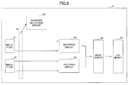
Fig. 8 , thefilter circuit 23 and the highfrequency filter circuits 63 may not be included. - Referring to
Figs. 3 through 8 , an outline of overall operations of the circuit blocks included in theillumination lamp 2 has been described above. Next, referring toFig. 9 , characteristic operations of theillumination lamp 2 will be described. It should be noted that, inFig. 9 , wire connections only for the major circuits of theillumination lamp 2 according to the embodiment are shown and an illustration of wire connections for portions not related to the characteristic operations is omitted. - In
Fig. 9 , theterminals mouthpiece 21 of theillumination lamp 2 are inserted, engaged with, and electrically connected to therespective terminals socket 51 of theillumination fixture 5. Similarly, theterminals mouthpiece 22 of theillumination lamp 2 are inserted into, engaged with, and electrically connected to therespective terminals socket 52 of theillumination fixture 5. - The
rectifier circuits fluorescent ballast 50 is other than an inverter ballast for fluorescent lamps, therectifier circuits mouthpieces Fig. 9 ). Further, a rectified voltage V1 rectified by therectifier circuits side wire connection 31 and the minusside wire connection 32 which are output units of therectifier circuits Fig. 9 ), supplied to theLED module 27. - On the other hand, in the case where the
fluorescent ballast 50 is an inverter ballast for fluorescent lamps, therectifier circuits filter circuit 23. Further, the rectified voltage V1 rectified by therectifier circuits side wire connection 31 and the minusside wire connection 32, and, through the switching circuit 33 (thedrive circuit 26 is by-passed), supplied to theLED module 27. - It should be noted that the switching circuit 33 is inserted in the plus
side wire connection 31, and is a circuit a state of which is switched between a conductive state and a non-conductive state according to the voltage V1 (voltage between the plusside wire connection 31 and the minus side wire connection 32) rectified by therectifier circuits LED module 27. When the voltage V1 is equal to or more than the predetermined voltage, the switching circuit 33 is conductive and allows the current to flow in theLED module 27; and after the switching circuit 33 become conductive, it keeps being conductive even if the voltage V1 changes to be less than the predetermined voltage. - The switching circuit 33 can be by-passed by using the
switching circuit 61. InFig. 9 , as an example, the switching circuit 33 includes a silicon diode alternating current bi-directional switch (SIDAC (registered trademark)). It should be noted that the switching circuit 33 may include not only a single switching element like a SIDAC but also multiple elements. - For example, the switching circuit 33 may include a detection unit for detecting the voltage V1 and a switch unit for switching between a conductive state and a non-conductive state of the plus
side wire connection 31. The circuit switches to a conductive state when the voltage V1 is equal to or more than a predetermined voltage, and continues in a conductive state even the voltage V1 becomes less than the predetermined voltage after the voltage V1 has become equal to or more than the predetermined voltage. Further, a part of the circuit may include an element such as a thyristor or a triode for alternating current (TRIAC). - The
LED module 27 includes a plurality of serial connection units in which a plurality oflight emitting diodes 271 are connected in series between the plusside wire connection 31 and the minus side wire connection 32 (6light emitting diodes 271 are connected in series inFig. 9 ). Further, the serial connection units are connected in parallel. When the switching circuit 33 switches to a conductive state, current flows in thelight emitting diodes 271, and light is emitted. - It should be noted that in the case where the
fluorescent ballast 50 is an inverter ballast for fluorescent lamps, at the startup of the inverter ballast for fluorescent lamps, a low voltage (voltage V1 = about 5 to 10 V) for preheating is applied, and after that, the voltage V1 becomes a little less than 200 V. Afterwards, the voltage V1 gradually increases to a little more than 200 V, and transitions to a stable operation. In the stable operation of a fluorescent lamp, a voltage a little more than 200 V is continuously applied. - There is an inverter ballast for fluorescent lamps which performs an anomaly detection at the startup. In the case where a fluorescent lamp is connected to an inverter ballast for fluorescent lamps, current does not flow in the fluorescent lamp. Therefore, in the case where an
illumination lamp 2 is connected to the inverter ballast for fluorescent lamps, it is necessary to make the same things happen as in the case where a fluorescent lamp is connected to the inverter ballast for fluorescent lamps. If different things happen, the inverter ballast for fluorescent lamps may detect an anomaly, a protection operation may be performed, and theillumination lamp 2 may not be turned on. - Therefore, in order to make the same things happen (that is, in order not to make the current flow), the switching circuit 33 is included. Further, the predetermined voltage with which the switching circuit 33 switches to a conductive state is set greater than a voltage the inverter ballast for fluorescent lamps outputs at the startup, and less than a voltage the inverter ballast for fluorescent lamps outputs when it transitions from the startup operation to the stable operation.
- For example, as the switching circuit 33, a SIDAC, a breakover voltage of which is 200 V, may be used. In this case, when the voltage V1 is less than the SIDAC breakover voltage, 200 V, current does not flow from the inverter ballast for fluorescent lamps to the
rectifier circuits rectifier circuits - The voltage V1 applied by the inverter ballast for fluorescent lamps at the startup is a little less than 200 V at most. Therefore, the current does not flow from the inverter ballast for fluorescent lamps to the
rectifier circuits illumination lamp 2 is not turned on. - Afterwards, the voltage V1 applied by the inverter ballast for fluorescent lamps gradually increases to a little more than 200 V that is the breakover voltage of the SIDAC, and transitions to a stable operation. When the voltage V1 is equal to or more than the breakover voltage of the SIDAC, current flows from the inverter ballast for fluorescent lamps to the
rectifier circuits LED module 27 through the SIDAC. At this time, the voltage V1 applied by the inverter ballast for fluorescent lamps decreases to a voltage in which a voltage-drop voltage at the SIDAC (a little less than 1 V) is added to a sum of the forward voltages of thelight emitting diodes 271 included in each of the serial connection units of theLED module 27. - As described above, in the
illumination lamp 2 according to the first embodiment, by using the switching circuit 33, it becomes possible to avoid a situation in which theillumination lamp 2 is not turned on by having an anomaly detected by the anomaly detection performed at the startup of the inverter ballast for fluorescent lamps. In this way, theLED module 27 is capable of providing stable illumination. - Further, the sum of the forward voltages of the
light emitting diodes 271 included in each of the serial connection units of theLED module 27 is set to be a voltage (e.g., about 80 V) less than a voltage normally applied at the stable operation of a fluorescent lamp (a little more than 200 V). Therefore, it becomes possible to make a voltage when the inverter ballast for fluorescent lamps transitions to a stable operation (e.g., 80 V + voltage-drop voltage at the SIDAC) less than a voltage of a case where a fluorescent lamp is used (about a little more than 200 V), and thus, energy saving can be achieved. - It should be noted that it is preferable that, in the case where the switching circuit 33 is a SIDAC, the breakover voltage be about 200 V. The more the breakover voltage decreases from 200 V, the more increases the likelihood of the breakover voltage being less than a voltage output by the inverter ballast for fluorescent lamps at the startup, and the protection operation is performed as a result of anomaly detection of the inverter ballast for fluorescent lamps. Further, the more the breakover voltage increases above 200 V, the more increases the likelihood of the voltage output by the inverter ballast for fluorescent lamps when it transitions from the startup to a stable operation cannot exceed the breakover voltage, and the current is not provided to the
illumination lamp 2 and theillumination lamp 2 is not turned on. - As described above, although preferred embodiments and modified examples thereof have been described in detail, the present invention is not limited to the above embodiments and modified examples, and various modifications and replacements may be applied to the above embodiments and modified examples without departing from the scope of the present invention.
- For example, in the above embodiments, as an example of the illumination lamp, an illumination lamp is shown, which is capable of connecting to any one of the fluorescent glow ballast, the fluorescent rapid ballast, the fluorescent inverter ballast and the commercial AC power. It should be noted that the present invention can be applied to an illumination lamp capable of being connected to at least an inverter ballast for fluorescent lamps. In other words, the present invention can be applied to an illumination lamp which can be connected to only the inverter ballast for fluorescent lamps, and also applied to an illumination lamp which can be connected to not only the inverter ballast for fluorescent lamps but also other fluorescent ballasts or the commercial AC power.
- Further, in the case of the illumination lamp capable of being connected to only an inverter ballast for fluorescent lamps, only necessary units in the circuit blocks shown in
FIGs. 3 through 8 may be included. For example, theinverter detection circuit 28, therapid detection circuit 29, thefilter circuit 23, thedrive circuit 26 or the like, may not be included. - The present invention is not limited to the specifically disclosed embodiments, and variations and modifications may be made without departing from the scope of the present invention.
- The present application is based on and claims the benefit of priority of Japanese Priority Application No.
2015-092645 filed on April 30, 2015
Claims (8)
- An illumination lamp connectable to an inverter ballast for fluorescent lamps, the illumination lamp comprising:a light emitting diode;a rectifier circuit configured to rectify an AC voltage supplied by the inverter ballast for fluorescent lamps and supply the rectified voltage to the light emitting diode; anda switching circuit configured to be in a non-conductive state when the rectified voltage from the rectifier circuit is less than a predetermined voltage and not allow current to flow in the light emitting diode, to switch to a conductive state when the rectified voltage from the rectifier circuit is equal to or greater than the predetermined voltage and allow the current to flow in the light emitting diode, and to continue in the conductive state even when the rectified voltage changes to be less than the predetermined voltage after switching to the conductive state.
- The illumination lamp according to claim 1, wherein
after the switching circuit has switched to the conductive state, the rectified voltage decreases to a voltage in which a voltage-drop voltage at the switching circuit is added to a forward direction voltage of the light emitting diode. - The illumination lamp according to claim 1, wherein
the predetermined voltage is set greater than a voltage output by the inverter ballast for fluorescent lamps at a startup and less than a voltage output by the inverter ballast for fluorescent lamps when the inverter ballast for fluorescent lamps transitions from a startup operation to a stable operation. - The illumination lamp according to claim 2, wherein the predetermined voltage is 200 V.
- The illumination lamp according to claim 3, wherein the predetermined voltage is 200 V.
- The illumination lamp according to claim 1, wherein
the switching circuit includes a single switching element. - An illumination apparatus comprising:the illumination lamp according to claim 1; andan illumination fixture the illumination lamp is attached to.
- An illumination control circuit used for an illumination lamp connectable to an inverter ballast for fluorescent lamps, the illumination control circuit comprising:a light emitting diode;a rectifier unit configured to rectify an AC voltage supplied by the inverter ballast for fluorescent lamps and supply the rectified voltage to the light emitting diode; anda switching unit configured to be in a non-conductive state when the rectified voltage from the rectifier unit is less than a predetermined voltage and not allow current to flow in the light emitting diode, to switch to a conductive state when the rectified voltage from the rectifier unit becomes equal to or greater than the predetermined voltage and allow the current to flow in the light emitting diode, and to continue in the conductive state even when the rectified voltage changes to be less than the predetermined voltage after switching to the conductive state.
Applications Claiming Priority (1)
| Application Number | Priority Date | Filing Date | Title |
|---|---|---|---|
| JP2015092645A JP6011676B1 (en) | 2015-04-30 | 2015-04-30 | Lighting lamp, lighting device, and lighting control circuit |
Publications (2)
| Publication Number | Publication Date |
|---|---|
| EP3089556A1 true EP3089556A1 (en) | 2016-11-02 |
| EP3089556B1 EP3089556B1 (en) | 2019-02-27 |
Family
ID=55854685
Family Applications (1)
| Application Number | Title | Priority Date | Filing Date |
|---|---|---|---|
| EP16167287.8A Not-in-force EP3089556B1 (en) | 2015-04-30 | 2016-04-27 | Illumination lamp, illumination apparatus, and illumination control circuit |
Country Status (2)
| Country | Link |
|---|---|
| EP (1) | EP3089556B1 (en) |
| JP (1) | JP6011676B1 (en) |
Cited By (1)
| Publication number | Priority date | Publication date | Assignee | Title |
|---|---|---|---|---|
| WO2020094438A1 (en) * | 2018-11-08 | 2020-05-14 | Signify Holding B.V. | A double ended retrofit light emitting diode, led, based lighting device for preventing an excess of leakage current during installation of said lighting device, as well as a corresponding method |
Families Citing this family (1)
| Publication number | Priority date | Publication date | Assignee | Title |
|---|---|---|---|---|
| JP7319418B2 (en) * | 2017-06-09 | 2023-08-01 | コイズミ照明株式会社 | lighting equipment |
Citations (5)
| Publication number | Priority date | Publication date | Assignee | Title |
|---|---|---|---|---|
| JPH11135274A (en) | 1997-10-30 | 1999-05-21 | Toshiba Tec Corp | Led light system |
| KR20090116259A (en) * | 2008-05-07 | 2009-11-11 | 주식회사 아모럭스 | Leakage current breaker when switching off from AC LED luminaire |
| JP2011060563A (en) * | 2009-09-10 | 2011-03-24 | Shindengen Electric Mfg Co Ltd | Led lighting device and led lighting method |
| JP2015179651A (en) * | 2014-02-26 | 2015-10-08 | 株式会社リコー | Illumination lamp, illumination device, and connection method of illumination lamp |
| WO2015156633A1 (en) * | 2014-04-10 | 2015-10-15 | 주식회사 아모센스 | Led lamp using switching circuit |
Family Cites Families (5)
| Publication number | Priority date | Publication date | Assignee | Title |
|---|---|---|---|---|
| WO2001045470A1 (en) * | 1999-12-14 | 2001-06-21 | Takion Co., Ltd. | Power supply and led lamp device |
| JP2012221940A (en) * | 2011-04-11 | 2012-11-12 | Shigenori Ishitobi | Fluorescent tube-type led illumination compatible with inverter-type fluorescent lamp fixture |
| JP2013120667A (en) * | 2011-12-07 | 2013-06-17 | Iwasaki Electric Co Ltd | Checker circuit detecting whether or not choke coil ballast is connected between socket for bulb and ac power supply, and checker device using the same |
| JP6007680B2 (en) * | 2012-08-31 | 2016-10-12 | 株式会社リコー | Lighting control circuit, illumination lamp using the lighting control circuit, and control method of the lighting control circuit |
| JP5266594B1 (en) * | 2012-10-25 | 2013-08-21 | 株式会社エム・システム技研 | LED lamp, lighting device including the LED lamp, and LED lamp current control method |
-
2015
- 2015-04-30 JP JP2015092645A patent/JP6011676B1/en not_active Expired - Fee Related
-
2016
- 2016-04-27 EP EP16167287.8A patent/EP3089556B1/en not_active Not-in-force
Patent Citations (5)
| Publication number | Priority date | Publication date | Assignee | Title |
|---|---|---|---|---|
| JPH11135274A (en) | 1997-10-30 | 1999-05-21 | Toshiba Tec Corp | Led light system |
| KR20090116259A (en) * | 2008-05-07 | 2009-11-11 | 주식회사 아모럭스 | Leakage current breaker when switching off from AC LED luminaire |
| JP2011060563A (en) * | 2009-09-10 | 2011-03-24 | Shindengen Electric Mfg Co Ltd | Led lighting device and led lighting method |
| JP2015179651A (en) * | 2014-02-26 | 2015-10-08 | 株式会社リコー | Illumination lamp, illumination device, and connection method of illumination lamp |
| WO2015156633A1 (en) * | 2014-04-10 | 2015-10-15 | 주식회사 아모센스 | Led lamp using switching circuit |
Cited By (3)
| Publication number | Priority date | Publication date | Assignee | Title |
|---|---|---|---|---|
| WO2020094438A1 (en) * | 2018-11-08 | 2020-05-14 | Signify Holding B.V. | A double ended retrofit light emitting diode, led, based lighting device for preventing an excess of leakage current during installation of said lighting device, as well as a corresponding method |
| CN113196884A (en) * | 2018-11-08 | 2021-07-30 | 昕诺飞控股有限公司 | Lighting device for preventing generation of excessive leakage current and corresponding method |
| US11483911B2 (en) | 2018-11-08 | 2022-10-25 | Signify Holding B.V. | Double ended retrofit light emitting diode, LED, based lighting device for preventing an excess of leakage current during installation of said lighting device, as well as a corresponding method |
Also Published As
| Publication number | Publication date |
|---|---|
| EP3089556B1 (en) | 2019-02-27 |
| JP2016212968A (en) | 2016-12-15 |
| JP6011676B1 (en) | 2016-10-19 |
Similar Documents
| Publication | Publication Date | Title |
|---|---|---|
| EP2914065B1 (en) | Illumination lamp and illumination apparatus | |
| US9560700B2 (en) | Illumination lamp and illumination device configured for rapid-start method | |
| CN105359625B (en) | For actuator device to be connected into external power source so as to the connection circuit of driving load especially LED unit | |
| JP2008277188A (en) | LED illumination lamp and lamp fixture using the LED illumination lamp | |
| WO2011014111A1 (en) | Lighting system | |
| US10136483B2 (en) | Solid-state lighting with auto-select settings for line voltage and ballast voltage | |
| CN109587866B (en) | Electronic driver for LED lighting module and LED lamp | |
| EP2838318A1 (en) | Lighting circuit and luminiare | |
| JP6614315B2 (en) | Illumination lamp and illumination device | |
| EP3089556B1 (en) | Illumination lamp, illumination apparatus, and illumination control circuit | |
| CN105874884B (en) | Lighting system including a switch with 2 power levels | |
| JP5924437B1 (en) | Lighting lamp, lighting device, and lighting control circuit | |
| JP6728299B2 (en) | Three-stage switching type omnidirectional LED lamp drive circuit | |
| KR20180015999A (en) | LED lamp control circuit compatible type fluorescent and lighting the use | |
| JP6354265B2 (en) | Illumination lamp, illumination device, and connection method of illumination lamp | |
| JP2017004611A (en) | Illumination lamp, illumination apparatus, lighting control circuit, and drive method for illumination lamp | |
| JP6331594B2 (en) | Illumination lamp, illumination device, and connection method of illumination lamp | |
| US10798794B2 (en) | LED lighting assembly and drive circuit | |
| US9198249B1 (en) | Lighting system including a driving device for driving a lighting appliance | |
| KR20180101699A (en) | Led lighting apparatus with interchangeability of fluorescent lamp | |
| JP3193669U (en) | AC-DC conversion power supply system for LED lamp | |
| CN111212499B (en) | Rectifier circuit for LED lamp driver | |
| CN109915797B (en) | Electronic driver for LED lighting module and LED lamp | |
| JP2016212966A (en) | Lighting lamp, lighting device, and lighting control circuit | |
| CN106870974B (en) | Multifunctional compatible lamp tube |
Legal Events
| Date | Code | Title | Description |
|---|---|---|---|
| PUAI | Public reference made under article 153(3) epc to a published international application that has entered the european phase |
Free format text: ORIGINAL CODE: 0009012 |
|
| 17P | Request for examination filed |
Effective date: 20160427 |
|
| AK | Designated contracting states |
Kind code of ref document: A1 Designated state(s): AL AT BE BG CH CY CZ DE DK EE ES FI FR GB GR HR HU IE IS IT LI LT LU LV MC MK MT NL NO PL PT RO RS SE SI SK SM TR |
|
| AX | Request for extension of the european patent |
Extension state: BA ME |
|
| STAA | Information on the status of an ep patent application or granted ep patent |
Free format text: STATUS: EXAMINATION IS IN PROGRESS |
|
| 17Q | First examination report despatched |
Effective date: 20170710 |
|
| REG | Reference to a national code |
Ref country code: DE Ref legal event code: R079 Ref document number: 602016010236 Country of ref document: DE Free format text: PREVIOUS MAIN CLASS: H05B0035000000 Ipc: H05B0033080000 |
|
| GRAP | Despatch of communication of intention to grant a patent |
Free format text: ORIGINAL CODE: EPIDOSNIGR1 |
|
| STAA | Information on the status of an ep patent application or granted ep patent |
Free format text: STATUS: GRANT OF PATENT IS INTENDED |
|
| RIC1 | Information provided on ipc code assigned before grant |
Ipc: F21Y 115/10 20160101ALI20180905BHEP Ipc: H05B 33/08 20060101AFI20180905BHEP |
|
| INTG | Intention to grant announced |
Effective date: 20180925 |
|
| GRAS | Grant fee paid |
Free format text: ORIGINAL CODE: EPIDOSNIGR3 |
|
| GRAA | (expected) grant |
Free format text: ORIGINAL CODE: 0009210 |
|
| STAA | Information on the status of an ep patent application or granted ep patent |
Free format text: STATUS: THE PATENT HAS BEEN GRANTED |
|
| AK | Designated contracting states |
Kind code of ref document: B1 Designated state(s): AL AT BE BG CH CY CZ DE DK EE ES FI FR GB GR HR HU IE IS IT LI LT LU LV MC MK MT NL NO PL PT RO RS SE SI SK SM TR |
|
| REG | Reference to a national code |
Ref country code: GB Ref legal event code: FG4D |
|
| REG | Reference to a national code |
Ref country code: CH Ref legal event code: EP |
|
| REG | Reference to a national code |
Ref country code: AT Ref legal event code: REF Ref document number: 1103281 Country of ref document: AT Kind code of ref document: T Effective date: 20190315 |
|
| REG | Reference to a national code |
Ref country code: IE Ref legal event code: FG4D |
|
| REG | Reference to a national code |
Ref country code: DE Ref legal event code: R096 Ref document number: 602016010236 Country of ref document: DE |
|
| REG | Reference to a national code |
Ref country code: NL Ref legal event code: MP Effective date: 20190227 |
|
| REG | Reference to a national code |
Ref country code: LT Ref legal event code: MG4D |
|
| PG25 | Lapsed in a contracting state [announced via postgrant information from national office to epo] |
Ref country code: NO Free format text: LAPSE BECAUSE OF FAILURE TO SUBMIT A TRANSLATION OF THE DESCRIPTION OR TO PAY THE FEE WITHIN THE PRESCRIBED TIME-LIMIT Effective date: 20190527 Ref country code: PT Free format text: LAPSE BECAUSE OF FAILURE TO SUBMIT A TRANSLATION OF THE DESCRIPTION OR TO PAY THE FEE WITHIN THE PRESCRIBED TIME-LIMIT Effective date: 20190627 Ref country code: FI Free format text: LAPSE BECAUSE OF FAILURE TO SUBMIT A TRANSLATION OF THE DESCRIPTION OR TO PAY THE FEE WITHIN THE PRESCRIBED TIME-LIMIT Effective date: 20190227 Ref country code: NL Free format text: LAPSE BECAUSE OF FAILURE TO SUBMIT A TRANSLATION OF THE DESCRIPTION OR TO PAY THE FEE WITHIN THE PRESCRIBED TIME-LIMIT Effective date: 20190227 Ref country code: SE Free format text: LAPSE BECAUSE OF FAILURE TO SUBMIT A TRANSLATION OF THE DESCRIPTION OR TO PAY THE FEE WITHIN THE PRESCRIBED TIME-LIMIT Effective date: 20190227 Ref country code: LT Free format text: LAPSE BECAUSE OF FAILURE TO SUBMIT A TRANSLATION OF THE DESCRIPTION OR TO PAY THE FEE WITHIN THE PRESCRIBED TIME-LIMIT Effective date: 20190227 |
|
| PG25 | Lapsed in a contracting state [announced via postgrant information from national office to epo] |
Ref country code: RS Free format text: LAPSE BECAUSE OF FAILURE TO SUBMIT A TRANSLATION OF THE DESCRIPTION OR TO PAY THE FEE WITHIN THE PRESCRIBED TIME-LIMIT Effective date: 20190227 Ref country code: HR Free format text: LAPSE BECAUSE OF FAILURE TO SUBMIT A TRANSLATION OF THE DESCRIPTION OR TO PAY THE FEE WITHIN THE PRESCRIBED TIME-LIMIT Effective date: 20190227 Ref country code: LV Free format text: LAPSE BECAUSE OF FAILURE TO SUBMIT A TRANSLATION OF THE DESCRIPTION OR TO PAY THE FEE WITHIN THE PRESCRIBED TIME-LIMIT Effective date: 20190227 Ref country code: GR Free format text: LAPSE BECAUSE OF FAILURE TO SUBMIT A TRANSLATION OF THE DESCRIPTION OR TO PAY THE FEE WITHIN THE PRESCRIBED TIME-LIMIT Effective date: 20190528 Ref country code: IS Free format text: LAPSE BECAUSE OF FAILURE TO SUBMIT A TRANSLATION OF THE DESCRIPTION OR TO PAY THE FEE WITHIN THE PRESCRIBED TIME-LIMIT Effective date: 20190627 Ref country code: BG Free format text: LAPSE BECAUSE OF FAILURE TO SUBMIT A TRANSLATION OF THE DESCRIPTION OR TO PAY THE FEE WITHIN THE PRESCRIBED TIME-LIMIT Effective date: 20190527 |
|
| REG | Reference to a national code |
Ref country code: AT Ref legal event code: MK05 Ref document number: 1103281 Country of ref document: AT Kind code of ref document: T Effective date: 20190227 |
|
| PG25 | Lapsed in a contracting state [announced via postgrant information from national office to epo] |
Ref country code: RO Free format text: LAPSE BECAUSE OF FAILURE TO SUBMIT A TRANSLATION OF THE DESCRIPTION OR TO PAY THE FEE WITHIN THE PRESCRIBED TIME-LIMIT Effective date: 20190227 Ref country code: IT Free format text: LAPSE BECAUSE OF FAILURE TO SUBMIT A TRANSLATION OF THE DESCRIPTION OR TO PAY THE FEE WITHIN THE PRESCRIBED TIME-LIMIT Effective date: 20190227 Ref country code: DK Free format text: LAPSE BECAUSE OF FAILURE TO SUBMIT A TRANSLATION OF THE DESCRIPTION OR TO PAY THE FEE WITHIN THE PRESCRIBED TIME-LIMIT Effective date: 20190227 Ref country code: EE Free format text: LAPSE BECAUSE OF FAILURE TO SUBMIT A TRANSLATION OF THE DESCRIPTION OR TO PAY THE FEE WITHIN THE PRESCRIBED TIME-LIMIT Effective date: 20190227 Ref country code: AL Free format text: LAPSE BECAUSE OF FAILURE TO SUBMIT A TRANSLATION OF THE DESCRIPTION OR TO PAY THE FEE WITHIN THE PRESCRIBED TIME-LIMIT Effective date: 20190227 Ref country code: CZ Free format text: LAPSE BECAUSE OF FAILURE TO SUBMIT A TRANSLATION OF THE DESCRIPTION OR TO PAY THE FEE WITHIN THE PRESCRIBED TIME-LIMIT Effective date: 20190227 Ref country code: ES Free format text: LAPSE BECAUSE OF FAILURE TO SUBMIT A TRANSLATION OF THE DESCRIPTION OR TO PAY THE FEE WITHIN THE PRESCRIBED TIME-LIMIT Effective date: 20190227 Ref country code: SK Free format text: LAPSE BECAUSE OF FAILURE TO SUBMIT A TRANSLATION OF THE DESCRIPTION OR TO PAY THE FEE WITHIN THE PRESCRIBED TIME-LIMIT Effective date: 20190227 |
|
| REG | Reference to a national code |
Ref country code: DE Ref legal event code: R079 Ref document number: 602016010236 Country of ref document: DE Free format text: PREVIOUS MAIN CLASS: H05B0033080000 Ipc: H05B0045000000 |
|
| REG | Reference to a national code |
Ref country code: DE Ref legal event code: R097 Ref document number: 602016010236 Country of ref document: DE |
|
| PG25 | Lapsed in a contracting state [announced via postgrant information from national office to epo] |
Ref country code: PL Free format text: LAPSE BECAUSE OF FAILURE TO SUBMIT A TRANSLATION OF THE DESCRIPTION OR TO PAY THE FEE WITHIN THE PRESCRIBED TIME-LIMIT Effective date: 20190227 Ref country code: SM Free format text: LAPSE BECAUSE OF FAILURE TO SUBMIT A TRANSLATION OF THE DESCRIPTION OR TO PAY THE FEE WITHIN THE PRESCRIBED TIME-LIMIT Effective date: 20190227 |
|
| REG | Reference to a national code |
Ref country code: CH Ref legal event code: PL |
|
| REG | Reference to a national code |
Ref country code: BE Ref legal event code: MM Effective date: 20190430 |
|
| PG25 | Lapsed in a contracting state [announced via postgrant information from national office to epo] |
Ref country code: AT Free format text: LAPSE BECAUSE OF FAILURE TO SUBMIT A TRANSLATION OF THE DESCRIPTION OR TO PAY THE FEE WITHIN THE PRESCRIBED TIME-LIMIT Effective date: 20190227 Ref country code: LU Free format text: LAPSE BECAUSE OF NON-PAYMENT OF DUE FEES Effective date: 20190427 Ref country code: MC Free format text: LAPSE BECAUSE OF FAILURE TO SUBMIT A TRANSLATION OF THE DESCRIPTION OR TO PAY THE FEE WITHIN THE PRESCRIBED TIME-LIMIT Effective date: 20190227 |
|
| PLBE | No opposition filed within time limit |
Free format text: ORIGINAL CODE: 0009261 |
|
| STAA | Information on the status of an ep patent application or granted ep patent |
Free format text: STATUS: NO OPPOSITION FILED WITHIN TIME LIMIT |
|
| PG25 | Lapsed in a contracting state [announced via postgrant information from national office to epo] |
Ref country code: LI Free format text: LAPSE BECAUSE OF NON-PAYMENT OF DUE FEES Effective date: 20190430 Ref country code: CH Free format text: LAPSE BECAUSE OF NON-PAYMENT OF DUE FEES Effective date: 20190430 |
|
| 26N | No opposition filed |
Effective date: 20191128 |
|
| PG25 | Lapsed in a contracting state [announced via postgrant information from national office to epo] |
Ref country code: SI Free format text: LAPSE BECAUSE OF FAILURE TO SUBMIT A TRANSLATION OF THE DESCRIPTION OR TO PAY THE FEE WITHIN THE PRESCRIBED TIME-LIMIT Effective date: 20190227 Ref country code: BE Free format text: LAPSE BECAUSE OF NON-PAYMENT OF DUE FEES Effective date: 20190430 |
|
| PG25 | Lapsed in a contracting state [announced via postgrant information from national office to epo] |
Ref country code: TR Free format text: LAPSE BECAUSE OF FAILURE TO SUBMIT A TRANSLATION OF THE DESCRIPTION OR TO PAY THE FEE WITHIN THE PRESCRIBED TIME-LIMIT Effective date: 20190227 |
|
| PG25 | Lapsed in a contracting state [announced via postgrant information from national office to epo] |
Ref country code: IE Free format text: LAPSE BECAUSE OF NON-PAYMENT OF DUE FEES Effective date: 20190427 |
|
| PGFP | Annual fee paid to national office [announced via postgrant information from national office to epo] |
Ref country code: DE Payment date: 20200420 Year of fee payment: 5 Ref country code: FR Payment date: 20200420 Year of fee payment: 5 |
|
| PGFP | Annual fee paid to national office [announced via postgrant information from national office to epo] |
Ref country code: GB Payment date: 20200427 Year of fee payment: 5 |
|
| PG25 | Lapsed in a contracting state [announced via postgrant information from national office to epo] |
Ref country code: CY Free format text: LAPSE BECAUSE OF FAILURE TO SUBMIT A TRANSLATION OF THE DESCRIPTION OR TO PAY THE FEE WITHIN THE PRESCRIBED TIME-LIMIT Effective date: 20190227 |
|
| PG25 | Lapsed in a contracting state [announced via postgrant information from national office to epo] |
Ref country code: HU Free format text: LAPSE BECAUSE OF FAILURE TO SUBMIT A TRANSLATION OF THE DESCRIPTION OR TO PAY THE FEE WITHIN THE PRESCRIBED TIME-LIMIT; INVALID AB INITIO Effective date: 20160427 Ref country code: MT Free format text: LAPSE BECAUSE OF FAILURE TO SUBMIT A TRANSLATION OF THE DESCRIPTION OR TO PAY THE FEE WITHIN THE PRESCRIBED TIME-LIMIT Effective date: 20190227 |
|
| REG | Reference to a national code |
Ref country code: DE Ref legal event code: R119 Ref document number: 602016010236 Country of ref document: DE |
|
| GBPC | Gb: european patent ceased through non-payment of renewal fee |
Effective date: 20210427 |
|
| PG25 | Lapsed in a contracting state [announced via postgrant information from national office to epo] |
Ref country code: DE Free format text: LAPSE BECAUSE OF NON-PAYMENT OF DUE FEES Effective date: 20211103 Ref country code: FR Free format text: LAPSE BECAUSE OF NON-PAYMENT OF DUE FEES Effective date: 20210430 Ref country code: GB Free format text: LAPSE BECAUSE OF NON-PAYMENT OF DUE FEES Effective date: 20210427 |
|
| PG25 | Lapsed in a contracting state [announced via postgrant information from national office to epo] |
Ref country code: MK Free format text: LAPSE BECAUSE OF FAILURE TO SUBMIT A TRANSLATION OF THE DESCRIPTION OR TO PAY THE FEE WITHIN THE PRESCRIBED TIME-LIMIT Effective date: 20190227 |