EP3089297A1 - Electrical coupler, power converter, and method - Google Patents
Electrical coupler, power converter, and method Download PDFInfo
- Publication number
- EP3089297A1 EP3089297A1 EP16167249.8A EP16167249A EP3089297A1 EP 3089297 A1 EP3089297 A1 EP 3089297A1 EP 16167249 A EP16167249 A EP 16167249A EP 3089297 A1 EP3089297 A1 EP 3089297A1
- Authority
- EP
- European Patent Office
- Prior art keywords
- layer
- resistance
- frequency range
- current
- coupler
- Prior art date
- Legal status (The legal status is an assumption and is not a legal conclusion. Google has not performed a legal analysis and makes no representation as to the accuracy of the status listed.)
- Granted
Links
- 238000000034 method Methods 0.000 title claims description 14
- 229910000831 Steel Inorganic materials 0.000 claims description 10
- 239000010959 steel Substances 0.000 claims description 10
- RYGMFSIKBFXOCR-UHFFFAOYSA-N Copper Chemical compound [Cu] RYGMFSIKBFXOCR-UHFFFAOYSA-N 0.000 claims description 9
- 229910052802 copper Inorganic materials 0.000 claims description 9
- 239000010949 copper Substances 0.000 claims description 9
- 239000003990 capacitor Substances 0.000 claims description 8
- 239000012212 insulator Substances 0.000 claims description 5
- 238000003466 welding Methods 0.000 claims description 2
- 230000000087 stabilizing effect Effects 0.000 claims 1
- 238000013016 damping Methods 0.000 description 11
- 239000000463 material Substances 0.000 description 9
- 239000004020 conductor Substances 0.000 description 6
- 238000001816 cooling Methods 0.000 description 5
- 230000002500 effect on skin Effects 0.000 description 4
- 230000035699 permeability Effects 0.000 description 4
- 238000012360 testing method Methods 0.000 description 4
- 230000000694 effects Effects 0.000 description 3
- 238000012546 transfer Methods 0.000 description 3
- 230000007423 decrease Effects 0.000 description 2
- 230000005284 excitation Effects 0.000 description 2
- 239000007788 liquid Substances 0.000 description 2
- 238000004519 manufacturing process Methods 0.000 description 2
- 239000002184 metal Substances 0.000 description 2
- 229910052751 metal Inorganic materials 0.000 description 2
- 229910001092 metal group alloy Inorganic materials 0.000 description 2
- 230000005012 migration Effects 0.000 description 2
- 238000013508 migration Methods 0.000 description 2
- 230000010355 oscillation Effects 0.000 description 2
- 238000003825 pressing Methods 0.000 description 2
- 230000008569 process Effects 0.000 description 2
- 230000009467 reduction Effects 0.000 description 2
- 239000007787 solid Substances 0.000 description 2
- 238000001228 spectrum Methods 0.000 description 2
- 230000004308 accommodation Effects 0.000 description 1
- 230000008901 benefit Effects 0.000 description 1
- 238000005219 brazing Methods 0.000 description 1
- 238000001311 chemical methods and process Methods 0.000 description 1
- 238000006243 chemical reaction Methods 0.000 description 1
- 239000011248 coating agent Substances 0.000 description 1
- 238000000576 coating method Methods 0.000 description 1
- 230000003247 decreasing effect Effects 0.000 description 1
- 238000010586 diagram Methods 0.000 description 1
- 230000005669 field effect Effects 0.000 description 1
- 230000020169 heat generation Effects 0.000 description 1
- 238000009434 installation Methods 0.000 description 1
- 238000010297 mechanical methods and process Methods 0.000 description 1
- 230000005226 mechanical processes and functions Effects 0.000 description 1
- 230000007246 mechanism Effects 0.000 description 1
- 229910044991 metal oxide Inorganic materials 0.000 description 1
- 150000004706 metal oxides Chemical class 0.000 description 1
- 238000012986 modification Methods 0.000 description 1
- 230000004048 modification Effects 0.000 description 1
- 230000004044 response Effects 0.000 description 1
- 239000004065 semiconductor Substances 0.000 description 1
- 238000005476 soldering Methods 0.000 description 1
- 239000010935 stainless steel Substances 0.000 description 1
- 229910001220 stainless steel Inorganic materials 0.000 description 1
Images




Classifications
-
- H—ELECTRICITY
- H01—ELECTRIC ELEMENTS
- H01B—CABLES; CONDUCTORS; INSULATORS; SELECTION OF MATERIALS FOR THEIR CONDUCTIVE, INSULATING OR DIELECTRIC PROPERTIES
- H01B5/00—Non-insulated conductors or conductive bodies characterised by their form
- H01B5/16—Non-insulated conductors or conductive bodies characterised by their form comprising conductive material in insulating or poorly conductive material, e.g. conductive rubber
-
- H—ELECTRICITY
- H01—ELECTRIC ELEMENTS
- H01B—CABLES; CONDUCTORS; INSULATORS; SELECTION OF MATERIALS FOR THEIR CONDUCTIVE, INSULATING OR DIELECTRIC PROPERTIES
- H01B1/00—Conductors or conductive bodies characterised by the conductive materials; Selection of materials as conductors
- H01B1/02—Conductors or conductive bodies characterised by the conductive materials; Selection of materials as conductors mainly consisting of metals or alloys
- H01B1/026—Alloys based on copper
-
- H—ELECTRICITY
- H01—ELECTRIC ELEMENTS
- H01G—CAPACITORS; CAPACITORS, RECTIFIERS, DETECTORS, SWITCHING DEVICES, LIGHT-SENSITIVE OR TEMPERATURE-SENSITIVE DEVICES OF THE ELECTROLYTIC TYPE
- H01G4/00—Fixed capacitors; Processes of their manufacture
- H01G4/33—Thin- or thick-film capacitors (thin- or thick-film circuits; capacitors without a potential-jump or surface barrier specially adapted for integrated circuits, details thereof, multistep manufacturing processes therefor)
-
- H—ELECTRICITY
- H01—ELECTRIC ELEMENTS
- H01G—CAPACITORS; CAPACITORS, RECTIFIERS, DETECTORS, SWITCHING DEVICES, LIGHT-SENSITIVE OR TEMPERATURE-SENSITIVE DEVICES OF THE ELECTROLYTIC TYPE
- H01G4/00—Fixed capacitors; Processes of their manufacture
- H01G4/35—Feed-through capacitors or anti-noise capacitors
-
- H—ELECTRICITY
- H02—GENERATION; CONVERSION OR DISTRIBUTION OF ELECTRIC POWER
- H02M—APPARATUS FOR CONVERSION BETWEEN AC AND AC, BETWEEN AC AND DC, OR BETWEEN DC AND DC, AND FOR USE WITH MAINS OR SIMILAR POWER SUPPLY SYSTEMS; CONVERSION OF DC OR AC INPUT POWER INTO SURGE OUTPUT POWER; CONTROL OR REGULATION THEREOF
- H02M1/00—Details of apparatus for conversion
- H02M1/12—Arrangements for reducing harmonics from AC input or output
- H02M1/126—Arrangements for reducing harmonics from AC input or output using passive filters
-
- H—ELECTRICITY
- H02—GENERATION; CONVERSION OR DISTRIBUTION OF ELECTRIC POWER
- H02M—APPARATUS FOR CONVERSION BETWEEN AC AND AC, BETWEEN AC AND DC, OR BETWEEN DC AND DC, AND FOR USE WITH MAINS OR SIMILAR POWER SUPPLY SYSTEMS; CONVERSION OF DC OR AC INPUT POWER INTO SURGE OUTPUT POWER; CONTROL OR REGULATION THEREOF
- H02M7/00—Conversion of AC power input into DC power output; Conversion of DC power input into AC power output
- H02M7/42—Conversion of DC power input into AC power output without possibility of reversal
- H02M7/44—Conversion of DC power input into AC power output without possibility of reversal by static converters
- H02M7/48—Conversion of DC power input into AC power output without possibility of reversal by static converters using discharge tubes with control electrode or semiconductor devices with control electrode
Definitions
- Embodiments of the subject matter disclosed herein generally relate to an electrical coupler, and more particularly, to a bus bar for a power converter.
- Modem power converters incorporate a variety of electrical components to convert energy from an electrical source into usable electrical power for a load.
- some of these components may introduce harmonic excitations to the converter's framework of electrical couplers and capacitors.
- the response of the couplers and capacitors to these excitations may have to be explicitly damped with resistors.
- heat generated by damping is often significant and is another potential source of damage to the converter. Accordingly, damping is often accompanied by additional cooling equipment.
- damping and cooling a power converter increases costs and decreases converter efficiency. These measures also compromise converter power density, particularly when liquid cooling is implemented.
- an electric coupler includes a body, a first electrical path through the body having a first resistance to electric current within a first frequency range, and a second electrical path through the body having a second resistance to electric current within a second frequency range.
- a power converter may include an input stage configured to receive alternating or direct current, an output stage configured to output alternating or direct current and a coupler between the input stage and the output stage.
- the coupler may include a first body, a first electrical path through the first body having a first resistance to electric current within a first frequency range and, a second electrical path through the first body having a second resistance to electric current within a second frequency range.
- a method of conducting electrical current through a bus bar of a power converter can include conducting electric current within a first frequency range through a first layer of the bus bar at a first resistance and conducting electric current within a second frequency range through a second layer of the bus bar at a second resistance.
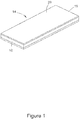
- an electrical coupler 14 defines an elongate body 20 having a rectangular cross section.
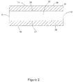
- Elongate body 20 includes an inner layer 22 and two outer layers 28 and 32.
- Inner layer 22 is made of a first electrically conductive material such as a metal or a metallic alloy, and outer layers 28 and 32 are made of a second electrically conductive material, such as a metal or a metallic alloy.
- the material of inner layer 22 may have a higher electrical conductivity than outer layers 28 and 32.
- Layers 22, 28, and 32 are electrically connected at the ends 16 and 18 of body 20 such that current entering body 20 may migrate to any of layers 22, 28, and 32.
- Layers 22, 28, and 32 may also be electrically connected along the interfaces 24 and 26 between the layers to allow for further migration and control of current flow across layers 22, 28, and 32.
- coupler 14 provides at least two electrical paths between the longitudinal ends 16 and 18. Specifically, a first electrical path is provided through the first material of inner layer 22 and a second electrical path is provided through the second material of outer layers 28 and 32.
- high frequency current components travelling through body 20 will cause an inductance within each of the outer layers 28 and 32.
- the inductance of each of first body 320 and second body 340 may be used to further force the migration of higher frequency components of the current toward the outer surface of layers 328, 332, 348 and 352 according to the so-called proximity effect. Therefore, reducing the distance between first body 320 and second body 340 will cause a corresponding reduction in the skin depth of the high frequency current within outer layers 328, 332, 348 and 352.
- each layer 22, 28, and 32 may also be configured with different materials, geometric dimensions, resistivity, and magnetic permeability to control or process longitudinal current flow through body 20 from end 16 to end 18.
- each layer of electrical coupler 14 may be configured to provide a frequency specific resistance.
- the skin effect and the proximity effect will tend to force higher frequency components of current to the outer surfaces of the outer layers 28 and 32.
- the outer layers 28 and 32 may be configured, for example, with a higher resistance such that current having a frequency above a certain predetermined magnitude will pass relatively freely from end 16 to end 18 within outer layers 28 and 32.
- the material, geometric dimensions (length, width and height), resistivity, and magnetic permeability of outer layers 28 and 32 may be configured such that almost all of the current within a preselected frequency range will flow in outer layers 28 and 32.
- Outer layers 28 and 32 may be further configured to provide a resistance to this current or to allow this current to pass relatively freely through body 20.
- inner layer 22 may be configured such that almost all of the current within a lower preselected frequency range will flow through inner layer 22.
- Inner layer 22 may be further configured to provide a resistance to this current or to allow this current to pass relatively freely through body 20.
- the preselected frequency range of outer layers 28 and 32 and the preselected frequency range of inner layer 22 may overlap to provide body 20 with an overall resistance which may behave in a predictable manner, e.g., linearly, with frequency.
- coupler 14 is enhanced by the rectangular cross section of each of layers 22, 28, and 32 which provide adequate surface area for optimizing skin effect, skin depth, and the proximity effect on current flowing through coupler 14 while also providing low volume for reduced material usage. Further, in embodiments where the interface between layers 22, 28, and 32 includes an air gap, manufacturing and assembly of connector 14 can be readily performed using a variety of manufacturing techniques without concern for whether or not electrical connectivity is maintained along interfaces 24 and 26. Exemplary methods of connecting second layer 28 and third layer 32 to first layer 22 include chemical processes such as coating, adhering, welding, brazing, or soldering and/or mechanical processes such as clamping, fastening or banding.
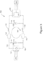
- FIG. 3 shows a schematic diagram of a power converter circuit 100.
- Power circuit 100 includes an input stage 101 that may receive fixed frequency AC current from AC source 103 and an output stage 102 that may provide variable frequency AC current to an AC load 104.
- Input stage 101 may include a three-phase rectifier (not shown) and output stage 102 may include six phase legs that contain metal oxide semiconductor field effect transistors (MOSFETs), insulated gate bipolar transistors (IGBTs), integrated gate commutated thyristors (IGCTs) and/or any other power device suitable for use in pulse width modulation.
- MOSFETs metal oxide semiconductor field effect transistors
- IGBTs insulated gate bipolar transistors
- IGCTs integrated gate commutated thyristors
- the input stage 101 is connected to the output stage 102 by first and second DC buses 106 and 108.
- First and second capacitor legs 110 and 112 extend between first and second DC buses 106 and 108 and include capacitor banks 114 and 116.
- a current loop 130 in power converter 100 is formed by first capacitor leg 110, first bus 106, second capacitor leg 112, and second bus 108.
- Each bus 106 and 108 may behave as an inductor 132 and 134 and, assuming a balanced inductance provided by each bus, may be said to have an inductance 1 ⁇ 2 L.
- first and second capacitor banks 114 and 116 may be said to each have a capacitance 1 ⁇ 2 C.
- the pulse width modulated power signal created by the aforementioned components in the first stage 101 of the power converter 100 may create current oscillations at or near the resonant frequency.
- a pair of resistors 140 and 142 may be incorporated in the power converter 100 such that a balanced RLC circuit is formed with each resistor having a resistance 1 ⁇ 2 R.
- the inclusion of resistors 132 and 134 within the current loop 130 allows for current oscillations at or near the resonant frequency to be damped thereby preventing damage to the power converter.
- bus bars 106 and 108 may be of sufficient length that the addition of explicit damping resistors will be required.
- the first and second stages 101 and 102 may be located in separate equipment cabinets that are interconnected by the bus bars 106 and 108.
- a larger damping resistance may be implemented to the current loop by the inclusion of a highly resistive conductor, such as stainless steel, in series with each bus bar.
- a highly resistive conductor such as stainless steel
- the loss in energy from this damping resistance becomes significant.
- this lost energy is expressed as heat which, as previously discussed, may require extensive accommodations to ensure effective heat transfer away from sensitive components.
- some power converters may be outfitted with liquid cooling arrangements in order to provide sufficient heat transfer capacity for continuous high load operation.
- the damping resistors may interfere with the conduction of low-frequency current flow desired for optimum power converter operation.
- a coupler according to the present invention may be implemented in series with each bus bar 106 and 108 to provide resistance to components of the current having a frequency at or near the resonant frequency f of the power converter 100 while allowing remaining lower-frequency currents to pass through relatively unimpeded.
- FIG 4 shows an embodiment of a dual-conductor coupler 314 appropriate for inclusion in a power converter, such as power converter 100 shown in Figure 3 .
- Coupler 314 includes first and second electrical bodies 320 and 340 separated by an insulator 310.
- the first electrical body 320 includes a pair of outer layers 328 and 332 electrically connected to an inner layer 322.
- the second electrical body 340 includes a pair of outer layers 348 and 352 electrically connected to an inner layer 342.
- each of the first and second electrical bodies 320 and 340 is also secured to an insulator 310 to form coupler 314.
- the first electrical body 320 may be formed by pressing the outer layers 328 and 332 against the inner layer 322 and fastening the layers 328, 332 and 322 together at the ends 316 and 318
- the second electrical body 340 may be formed by pressing the outer layers 348 and 352 against the inner layer 342 and fastening the layers 348, 352 and 342 together at the ends 316 and 318.
- Each of the first and second electrical bodies 320 and 340 may then be adhered, fastened or otherwise secured to insulator 310.
- a prototype coupler 314 has been configured with outer layers 328, 332, 348 and 352 made of steel and with inner layers 322 and 342 made of copper.
- the high permeability of steel material allows high frequency current to be concentrated into a very thin skin depth within the outer layers 328 and 332 of the first electrical body 320 and the outer layers 348 and 352 of the second electrical body 340.
- coupler 314 may be configured to provide damping resistance to high frequency current which may be at or near the resonant frequency of the power converter 100.
- the copper layer 322 or 342 in each first and second electrical body 320 or 340 allows low frequency current to travel through coupler 314 relatively unimpeded.
- Figure 5 shows the results of a frequency sweep comparison test between a conventional copper bus bar, a steel resistor, and an electrical coupler according to the embodiment of Figure 2 .
- the conventional copper bus bar exhibits an effective resistance which remains below 1.0 micro-Ohms across the tested frequency spectrum.
- the steel resistor exhibits an initial relatively constant effective resistance of approximately 2.8 micro-Ohms between 400 and 1000 Hz. The effective resistance then increases with frequency through 7000 Hz.
- the electrical coupler according to the embodiment of Figure 2 provides an effective resistance which rises relatively linearly from 0.5 micro-Ohms at approximately 350 Hz through approximately 4.5 micro-Ohms at 7000 Hz.
- the resistance provided by the electrical coupler according to the embodiment of Figure 2 is between the resistance provided by the copper bus bar and the steel resistor across the tested frequency spectrum.
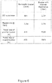
- Figure 6 shows the results of a power loss comparison test between a bus bar including coupler 314 and a conventional bus bar. Note that for current near the resonant frequency of approximately 7 kHz (seven kilohertz) both the bus bar including coupler 314 and the conventional bus bar provide an equivalent resistance of about 3.7 milli-Ohms. However, for low frequency or DC current flowing through each of the inner layers 322 and 342, the bus bar including coupler 314 provides a reduced resistance of approximately 90 micro-Ohms and the conventional bus bar provides a resistance of 3.7 milli-Ohms (a ratio of approximately 40-to-1).
- the decreased resistance to low frequency or DC current flowing through the bus bar with coupler 314 provides a power loss savings in the positive bus bar of approximately 1110 Watts and in the negative bus bar of approximately 760 Watts for a total average heat load reduction of approximately 60%. In addition to reduced energy costs, this increase in efficiency allows for the installation of smaller heat transfer mechanisms thereby further reducing equipment costs, increasing safety, and improving reliability of the power converter.
- coupler 314 may advantageously decrease the total portion of current requiring damping resistance.
- a method 1000 of conducting electrical current through a bus bar of a power converter may include conducting 1002 electric current within a first frequency range through a first layer of the bus bar at a first resistance and conducting 1004 electric current within a second frequency range through at least one of a second layer and a third layer of the bus bar at a second resistance.
- the electric current within the second frequency range may be conducted through both the second and third layers of the bus bar.
- the method 1000 may further include causing an inductance in one of the second and third layers to force current in the other of the second and third layers away from the first layer.
- the first resistance may be lower than the second resistance.
- the first frequency range may be lower than the second frequency range, or overlap the second frequency range.
- the second and third layers may be connected to opposed first and second sides of the first layer, respectively.
- the first layer may include copper and the second and third layers may include steel.
- the first, second and third layers may have a rectangular cross-section.
- each of the electrical bodies has been provided with a rectangular cross section and three layers.
- an electrical body according to the present invention may be provided with other cross-sectional shapes, for example, a coupler may have a circular or polygonal cross section.
- an electrical body may have less than three or more than three layers.
- an electrical body having a circular cross-sectional shape may have an innermost layer having a hollow or solid cross-sectional shape while one or more outer layers may each be provided in an annular or ring shaped cross-sectional profile.
- each layer may have a different cross-sectional profile, for example, an outer layer may have a polygonal or a faceted cross section, while an inner layer may have a circular or non-faceted cross-sectional profile.
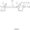
- FIGS 8 and 9 show an exemplary embodiment of a cylindrical electrical coupler 414 including an inner solid copper layer 422 and an outer steel layer 428. Each end of cylindrical coupler 414 includes a threaded hole 52. Coupler 414 may be fixed to a pair of support brackets 54 by a threaded fastener 56 provided with a fender washer 58 and lock washer 62. The configuration of cylindrical coupler 414 and brackets 54 allows coupler 414 to be readily replaced with another coupler having different characteristics.
Landscapes
- Engineering & Computer Science (AREA)
- Power Engineering (AREA)
- Microelectronics & Electronic Packaging (AREA)
- Manufacturing & Machinery (AREA)
- Inverter Devices (AREA)
- General Induction Heating (AREA)
Abstract
Description
- Embodiments of the subject matter disclosed herein generally relate to an electrical coupler, and more particularly, to a bus bar for a power converter.
- Modem power converters incorporate a variety of electrical components to convert energy from an electrical source into usable electrical power for a load. During the power conversion process, some of these components may introduce harmonic excitations to the converter's framework of electrical couplers and capacitors. In order to prevent potentially damaging resonances from occurring within the converter, the response of the couplers and capacitors to these excitations may have to be explicitly damped with resistors. However, heat generated by damping is often significant and is another potential source of damage to the converter. Accordingly, damping is often accompanied by additional cooling equipment. Thus, damping and cooling a power converter increases costs and decreases converter efficiency. These measures also compromise converter power density, particularly when liquid cooling is implemented.
- What is needed then is a component capable of introduction to a power converter or other electrical system, that provides adequate system damping while increasing efficiency and reducing heat generation.
- According to an exemplary embodiment, an electric coupler includes a body, a first electrical path through the body having a first resistance to electric current within a first frequency range, and a second electrical path through the body having a second resistance to electric current within a second frequency range.
- According to another exemplary embodiment, a power converter may include an input stage configured to receive alternating or direct current, an output stage configured to output alternating or direct current and a coupler between the input stage and the output stage. The coupler may include a first body, a first electrical path through the first body having a first resistance to electric current within a first frequency range and, a second electrical path through the first body having a second resistance to electric current within a second frequency range.
- According to another exemplary embodiment, a method of conducting electrical current through a bus bar of a power converter can include conducting electric current within a first frequency range through a first layer of the bus bar at a first resistance and conducting electric current within a second frequency range through a second layer of the bus bar at a second resistance.
- The accompanying drawings, which are incorporated in and constitute a part of the specification, illustrate one or more embodiments and, together with the description, explain these embodiments. In the drawings:
-
Figure 1 is a perspective view of an electrical coupler according to an exemplary embodiment. -
Figure 2 is a cross-sectional view of the electrical coupler shown inFigure 1 . -
Figure 3 is a schematic of a power converter. -
Figure 4 is a cross-sectional view of an electrical coupler according to another exemplary embodiment. -
Figure 5 shows frequency sweep test results of a conventional bus bar, a steel resistor, and the electrical coupler ofFigure 2 . -
Figure 6 shows converter thermal test results of a conventional bus bar compared with a bus bar in series with the electrical coupler ofFigure 4 . -
Figure 7 shows a method according to another exemplary embodiment. -
Figure 8 shows an electrical coupler according to another exemplary embodiment of the invention. -
Figure 9 shows a cross-sectional view of the electrical coupler shown inFigure 8 . - The following description of the exemplary embodiments refers to the accompanying drawings. The same reference numbers in different drawings identify the same or similar elements. The following detailed description does not limit the invention. Instead, the scope of the invention is defined by the appended claims. The following embodiments are discussed, for simplicity, with regard to the terminology and structure of power converter systems. However, the embodiments to be discussed next are not limited to these exemplary systems, but may be applied to other systems.
- Reference throughout the specification to "one embodiment" or "an embodiment" means that a particular feature, structure, or characteristic described in connection with an embodiment is included in at least one embodiment of the subject matter disclosed. Thus, the appearance of the phrases "in one embodiment" or "in an embodiment" in various places throughout the specification is not necessarily referring to the same embodiment. Further, the particular features, structures or characteristics may be combined in any suitable manner in one or more embodiments.
- An exemplary embodiment of an
electrical coupler 14 according to the present invention is shown inFigures 1 and2 . Therein, anelectrical coupler 14 defines anelongate body 20 having a rectangular cross section.Elongate body 20 includes aninner layer 22 and twoouter layers -
Inner layer 22 is made of a first electrically conductive material such as a metal or a metallic alloy, andouter layers inner layer 22 may have a higher electrical conductivity thanouter layers Layers ends body 20 such that current enteringbody 20 may migrate to any oflayers Layers interfaces layers - As may be appreciated from
Figures 1 and2 ,coupler 14 provides at least two electrical paths between thelongitudinal ends inner layer 22 and a second electrical path is provided through the second material ofouter layers - Even though two electrical paths are provided by
layers layers ends electrical body 20 to behave similarly to a traditional single material conductor. Specifically, higher frequency components of the current flowing withinelectrical body 20 may migrate, according to the so-called skin effect, from theinner layer 22 to theouter layers - Also, high frequency current components travelling through
body 20 will cause an inductance within each of theouter layers Figure 4 , the inductance of each offirst body 320 andsecond body 340 may be used to further force the migration of higher frequency components of the current toward the outer surface oflayers first body 320 andsecond body 340 will cause a corresponding reduction in the skin depth of the high frequency current withinouter layers - In addition to controlling skin effect and skin depth of electrical current according to frequency, each
layer body 20 fromend 16 toend 18. - In particular, each layer of
electrical coupler 14 may be configured to provide a frequency specific resistance. As discussed above, the skin effect and the proximity effect will tend to force higher frequency components of current to the outer surfaces of theouter layers outer layers end 16 to end 18 withinouter layers outer layers outer layers Outer layers body 20. Similarly, the material, geometric dimensions (length, width and height), resistivity, and magnetic permeability ofinner layer 22 may be configured such that almost all of the current within a lower preselected frequency range will flow throughinner layer 22.Inner layer 22 may be further configured to provide a resistance to this current or to allow this current to pass relatively freely throughbody 20. The preselected frequency range ofouter layers inner layer 22 may overlap to providebody 20 with an overall resistance which may behave in a predictable manner, e.g., linearly, with frequency. - The versatility of
coupler 14 is enhanced by the rectangular cross section of each oflayers coupler 14 while also providing low volume for reduced material usage. Further, in embodiments where the interface betweenlayers connector 14 can be readily performed using a variety of manufacturing techniques without concern for whether or not electrical connectivity is maintained alonginterfaces second layer 28 andthird layer 32 tofirst layer 22 include chemical processes such as coating, adhering, welding, brazing, or soldering and/or mechanical processes such as clamping, fastening or banding. -
Electrical coupler 14 may provide particular advantage in a power converter.Figure 3 shows a schematic diagram of apower converter circuit 100.Power circuit 100 includes aninput stage 101 that may receive fixed frequency AC current fromAC source 103 and anoutput stage 102 that may provide variable frequency AC current to anAC load 104.Input stage 101 may include a three-phase rectifier (not shown) andoutput stage 102 may include six phase legs that contain metal oxide semiconductor field effect transistors (MOSFETs), insulated gate bipolar transistors (IGBTs), integrated gate commutated thyristors (IGCTs) and/or any other power device suitable for use in pulse width modulation. - The
input stage 101 is connected to theoutput stage 102 by first andsecond DC buses second capacitor legs second DC buses capacitor banks - In operation, a
current loop 130 inpower converter 100 is formed byfirst capacitor leg 110,first bus 106,second capacitor leg 112, andsecond bus 108. Eachbus inductor second capacitor banks current loop 130 has an inductance L and capacitance C and the resonant frequency of the LC circuit in thepower converter 100 is provided by the Equation:
- During operation, the pulse width modulated power signal created by the aforementioned components in the
first stage 101 of thepower converter 100 may create current oscillations at or near the resonant frequency. In order to prevent potential damage caused by resonant operation ofpower converter 100, a pair ofresistors power converter 100 such that a balanced RLC circuit is formed with each resistor having a resistance ½ R. The inclusion ofresistors current loop 130 allows for current oscillations at or near the resonant frequency to be damped thereby preventing damage to the power converter. - For systems with very high resonant frequencies, the intrinsic resistance of normal bus bars may be enough to provide sufficient damping. However, bus bars 106 and 108 may be of sufficient length that the addition of explicit damping resistors will be required. For example, the first and
second stages - Of course, a larger damping resistance may be implemented to the current loop by the inclusion of a highly resistive conductor, such as stainless steel, in series with each bus bar. However, with increased power levels and increased bus bar lengths, the loss in energy from this damping resistance becomes significant. Moreover, this lost energy is expressed as heat which, as previously discussed, may require extensive accommodations to ensure effective heat transfer away from sensitive components. For example, and as previously mentioned, some power converters may be outfitted with liquid cooling arrangements in order to provide sufficient heat transfer capacity for continuous high load operation. In addition to the difficulty of dealing with the heat coming from a highly resistive conductor, the damping resistors may interfere with the conduction of low-frequency current flow desired for optimum power converter operation.
- In order to reduce and potentially obviate the need for such cooling, and to facilitate the delivery of low-frequency current, a coupler according to the present invention may be implemented in series with each
bus bar power converter 100 while allowing remaining lower-frequency currents to pass through relatively unimpeded. -
Figure 4 shows an embodiment of a dual-conductor coupler 314 appropriate for inclusion in a power converter, such aspower converter 100 shown inFigure 3 .Coupler 314 includes first and secondelectrical bodies insulator 310. The firstelectrical body 320 includes a pair ofouter layers inner layer 322. The secondelectrical body 340 includes a pair ofouter layers 348 and 352 electrically connected to aninner layer 342. As will be further described below, each of the first and secondelectrical bodies insulator 310 to formcoupler 314. - The first
electrical body 320 may be formed by pressing theouter layers inner layer 322 and fastening thelayers ends electrical body 340 may be formed by pressing theouter layers 348 and 352 against theinner layer 342 and fastening thelayers ends electrical bodies insulator 310. - A
prototype coupler 314 has been configured withouter layers inner layers outer layers electrical body 320 and theouter layers 348 and 352 of the secondelectrical body 340. Also, since steel has a resistivity approximately ten times larger in magnitude than copper,coupler 314 may be configured to provide damping resistance to high frequency current which may be at or near the resonant frequency of thepower converter 100. Thecopper layer electrical body coupler 314 relatively unimpeded. -
Figure 5 shows the results of a frequency sweep comparison test between a conventional copper bus bar, a steel resistor, and an electrical coupler according to the embodiment ofFigure 2 . As may be appreciated inFigure 5 , the conventional copper bus bar exhibits an effective resistance which remains below 1.0 micro-Ohms across the tested frequency spectrum. The steel resistor exhibits an initial relatively constant effective resistance of approximately 2.8 micro-Ohms between 400 and 1000 Hz. The effective resistance then increases with frequency through 7000 Hz. In contrast, the electrical coupler according to the embodiment ofFigure 2 provides an effective resistance which rises relatively linearly from 0.5 micro-Ohms at approximately 350 Hz through approximately 4.5 micro-Ohms at 7000 Hz. Also the resistance provided by the electrical coupler according to the embodiment ofFigure 2 is between the resistance provided by the copper bus bar and the steel resistor across the tested frequency spectrum. -
Figure 6 shows the results of a power loss comparison test between a busbar including coupler 314 and a conventional bus bar. Note that for current near the resonant frequency of approximately 7 kHz (seven kilohertz) both the busbar including coupler 314 and the conventional bus bar provide an equivalent resistance of about 3.7 milli-Ohms. However, for low frequency or DC current flowing through each of theinner layers bar including coupler 314 provides a reduced resistance of approximately 90 micro-Ohms and the conventional bus bar provides a resistance of 3.7 milli-Ohms (a ratio of approximately 40-to-1). The decreased resistance to low frequency or DC current flowing through the bus bar withcoupler 314 provides a power loss savings in the positive bus bar of approximately 1110 Watts and in the negative bus bar of approximately 760 Watts for a total average heat load reduction of approximately 60%. In addition to reduced energy costs, this increase in efficiency allows for the installation of smaller heat transfer mechanisms thereby further reducing equipment costs, increasing safety, and improving reliability of the power converter. - The flow of current through
coupler 314 is further facilitated by the three layer configuration shown inFigure 4 . Specifically, stray inductance of the firstelectrical body 320 may cancel out or otherwise interact with the stray inductance of the secondelectrical body 340 thereby causing the harmonic frequency of bus bar structure to be pushed away from the resonant frequency of thepower converter 100. Accordingly,coupler 314 may advantageously decrease the total portion of current requiring damping resistance. - Accordingly, and as shown in
Figure 7 , amethod 1000 of conducting electrical current through a bus bar of a power converter may include conducting 1002 electric current within a first frequency range through a first layer of the bus bar at a first resistance and conducting 1004 electric current within a second frequency range through at least one of a second layer and a third layer of the bus bar at a second resistance. The electric current within the second frequency range may be conducted through both the second and third layers of the bus bar. In some embodiments, themethod 1000 may further include causing an inductance in one of the second and third layers to force current in the other of the second and third layers away from the first layer. As described above, the first resistance may be lower than the second resistance. The first frequency range may be lower than the second frequency range, or overlap the second frequency range. The second and third layers may be connected to opposed first and second sides of the first layer, respectively. The first layer may include copper and the second and third layers may include steel. The first, second and third layers may have a rectangular cross-section. - In the embodiments of
Figures 1 to 4 , each of the electrical bodies has been provided with a rectangular cross section and three layers. However, an electrical body according to the present invention may be provided with other cross-sectional shapes, for example, a coupler may have a circular or polygonal cross section. Further, an electrical body may have less than three or more than three layers. For example, an electrical body having a circular cross-sectional shape may have an innermost layer having a hollow or solid cross-sectional shape while one or more outer layers may each be provided in an annular or ring shaped cross-sectional profile. Also, each layer may have a different cross-sectional profile, for example, an outer layer may have a polygonal or a faceted cross section, while an inner layer may have a circular or non-faceted cross-sectional profile. -
Figures 8 and9 show an exemplary embodiment of a cylindricalelectrical coupler 414 including an innersolid copper layer 422 and anouter steel layer 428. Each end ofcylindrical coupler 414 includes a threadedhole 52.Coupler 414 may be fixed to a pair ofsupport brackets 54 by a threadedfastener 56 provided with afender washer 58 andlock washer 62. The configuration ofcylindrical coupler 414 andbrackets 54 allowscoupler 414 to be readily replaced with another coupler having different characteristics. - The above-described embodiments are intended to be illustrative in all respects, rather than restrictive, of the present invention. All such variations and modifications are considered to be within the scope and spirit of the present invention as defined by the following claims. No element, act, or instruction used in the description of the present application should be construed as critical or essential to the invention unless explicitly described as such. Also, as used herein, the article "a" is intended to include one or more items.
Claims (15)
- An electric coupler (14; 314), comprising:a first body (20; 320);a first electrical path through the first body (20; 320) having a first resistance to electric current within a first frequency range; anda second electrical path through the first body (20; 320) having a second resistance to electric current within a second frequency range, wherein the first resistance is optionally lower than the second resistance, and the first frequency range is optionally lower than the second frequency range or overlaps the second frequency range.
- An electric coupler (14; 314) according to claim 1, wherein the first electrical path is defined by a first layer (22; 322) of the first body (20; 320) having opposed first and second sides, and wherein the second electrical path is defined by at least one of a second layer (28; 328) and a third layer (32; 332) of the first body (20; 320), the second layer (28; 328) being connected to the first side of the first layer (22; 322) and the third layer (32; 332) being connected to the second side of the first layer (22; 322).
- An electric coupler (14; 314) according to claim 2, wherein the second electrical path is defined by the second layer (28; 328) and the third layer (32; 332).
- An electric coupler (14; 314) according to claim 2 or claim 3, wherein an input end (16; 316) and an output end (18; 318) of the second and third layers (28, 32; 328, 332) are electrically connected to a respective input end and a respective output end of the first layer (22; 322) by at least one of welding, clamping, and fastening.
- An electric coupler (14; 314) according to any of claims 2 to 4, wherein the first layer (22; 322) includes copper and the second and third layers (28, 32; 328, 332) include steel.
- An electric coupler (314) according to any preceding claim, further comprising:a second body (340);a third electrical path through the second body (320) having a third resistance to electric current within a third frequency range; anda fourth electrical path through the second body (320) having a fourth resistance to electric current within a fourth frequency range, wherein the third resistance is optionally lower than the fourth resistance, and the third frequency range is optionally lower than the fourth frequency range or overlaps with the fourth frequency range.
- An electric coupler (314) according to claim 6, wherein the third electrical path is defined by a fourth layer (342) of the second body (340) having opposed first and second sides and the fourth electrical path is defined by at least one of a fifth layer (348) and a sixth layer (352) of the second body (340), the fifth layer (348) being connected to the first side of the fourth layer (342) and the sixth layer (352) being connected to the second side of the fourth layer (342).
- An electric coupler (314) according to claim 7, wherein the fourth electrical path is defined by the fifth layer (348) and the sixth layer (352).
- An electric coupler (314) according to any of claims 6 to 8, wherein the first resistance is substantially equal to the third resistance and the second resistance is substantially equal to the fourth resistance.
- An electric coupler (314) according to any of claims 6 to 9, wherein an insulator (310) is disposed between the first body (320) and the second body (340), the insulator (310) optionally being configured such that an inductance in one of the first body (320) and the second body (340) cancels at least a portion of an inductance in the other of the first body (320) and the second body (340).
- A power converter (100), comprising:an input stage (101) configured to receive alternating or direct current;an output stage (102) configured to output alternating or direct current;a voltage stabilizing capacitor (114, 116) between the input stage (101) and the output stage (102), andan electric coupler (14; 314) according to any preceding claim between the input stage and the output stage.
- A method of conducting electrical current through a bus bar of a power converter, the method comprising:conducting electric current within a first frequency range through a first layer (22; 322) of the bus bar at a first resistance; andconducting electric current within a second frequency range through at least one of a second layer (28; 328) and a third layer (32; 332) of the bus bar at a second resistance.
- A method according to claim 12, wherein an inductance in one of the second layer (28; 328) and the third layer (32; 332) forces current in the other of the second layer (28; 328) and the third layer (32; 332) away from the first layer (22; 322).
- A method according to claim 12 or claim 13, further comprising:conducting electric current within a third frequency range through a fourth layer (342) of the bus bar at a third resistance; andconducting electric current within a second frequency range through at least one of a fifth layer (348) and a sixth layer (352) of the bus bar at a fourth resistance.
- A method according to claim 14, wherein an inductance in one of the fifth layer (348) and the sixth layer (352) forces current in the other of the fifth layer (348) and the sixth layer (352) away from the fourth layer (342).
Applications Claiming Priority (1)
| Application Number | Priority Date | Filing Date | Title |
|---|---|---|---|
| CN201510206919.0A CN106160413A (en) | 2015-04-27 | 2015-04-27 | Circuit connector, power supply changeover device and method thereof |
Publications (2)
| Publication Number | Publication Date |
|---|---|
| EP3089297A1 true EP3089297A1 (en) | 2016-11-02 |
| EP3089297B1 EP3089297B1 (en) | 2018-03-07 |
Family
ID=55952967
Family Applications (1)
| Application Number | Title | Priority Date | Filing Date |
|---|---|---|---|
| EP16167249.8A Not-in-force EP3089297B1 (en) | 2015-04-27 | 2016-04-27 | Electrical coupler, power converter, and method |
Country Status (5)
| Country | Link |
|---|---|
| US (1) | US10475551B2 (en) |
| EP (1) | EP3089297B1 (en) |
| CN (1) | CN106160413A (en) |
| BR (1) | BR102016008503A2 (en) |
| CA (1) | CA2927272A1 (en) |
Families Citing this family (2)
| Publication number | Priority date | Publication date | Assignee | Title |
|---|---|---|---|---|
| EP4264640A1 (en) * | 2020-12-16 | 2023-10-25 | Robert Bosch GmbH | Conductor assembly, in particular for use in electric vehicles or hybrid vehicles |
| US20250140706A1 (en) * | 2023-10-26 | 2025-05-01 | Eaton Intelligent Power Limited | Bus system for a high-power converter circuit |
Citations (2)
| Publication number | Priority date | Publication date | Assignee | Title |
|---|---|---|---|---|
| US1561270A (en) * | 1920-09-17 | 1925-11-10 | Westinghouse Electric & Mfg Co | Bus bar |
| CN202608143U (en) * | 2012-04-16 | 2012-12-19 | 金川集团股份有限公司 | Copper coated stainless steel compound bar |
Family Cites Families (7)
| Publication number | Priority date | Publication date | Assignee | Title |
|---|---|---|---|---|
| JPS62164898A (en) | 1986-01-14 | 1987-07-21 | Tanaka Kikinzoku Kogyo Kk | Composite bus bar for electric conduction |
| JPS62164899A (en) | 1986-01-14 | 1987-07-21 | Tanaka Kikinzoku Kogyo Kk | Composite bus bar for electric conduction |
| JPS62164900A (en) | 1986-01-14 | 1987-07-21 | Tanaka Kikinzoku Kogyo Kk | Composite bus bar for electric conduction |
| JPS62164897A (en) | 1986-01-14 | 1987-07-21 | Tanaka Kikinzoku Kogyo Kk | Composite bus bar for electric conduction |
| JPH06309958A (en) | 1993-04-28 | 1994-11-04 | Hitachi Cable Ltd | Method for manufacturing conductive composite wire |
| US7265993B1 (en) * | 2005-05-16 | 2007-09-04 | Sun Microsystems, Inc. | Dispersive interconnect system for EMI reduction |
| US9240712B2 (en) * | 2012-12-13 | 2016-01-19 | Power Systems Technologies Ltd. | Controller including a common current-sense device for power switches of a power converter |
-
2015
- 2015-04-27 CN CN201510206919.0A patent/CN106160413A/en active Pending
-
2016
- 2016-04-14 CA CA2927272A patent/CA2927272A1/en not_active Abandoned
- 2016-04-15 BR BR102016008503A patent/BR102016008503A2/en not_active IP Right Cessation
- 2016-04-27 EP EP16167249.8A patent/EP3089297B1/en not_active Not-in-force
- 2016-04-27 US US15/139,781 patent/US10475551B2/en not_active Expired - Fee Related
Patent Citations (2)
| Publication number | Priority date | Publication date | Assignee | Title |
|---|---|---|---|---|
| US1561270A (en) * | 1920-09-17 | 1925-11-10 | Westinghouse Electric & Mfg Co | Bus bar |
| CN202608143U (en) * | 2012-04-16 | 2012-12-19 | 金川集团股份有限公司 | Copper coated stainless steel compound bar |
Also Published As
| Publication number | Publication date |
|---|---|
| EP3089297B1 (en) | 2018-03-07 |
| BR102016008503A2 (en) | 2016-11-01 |
| US10475551B2 (en) | 2019-11-12 |
| CN106160413A (en) | 2016-11-23 |
| CA2927272A1 (en) | 2016-10-27 |
| US20160315530A1 (en) | 2016-10-27 |
Similar Documents
| Publication | Publication Date | Title |
|---|---|---|
| US8693222B2 (en) | DC-DC converter, power supply unit and an information processing apparatus | |
| Mu et al. | Design of integrated transformer and inductor for high frequency dual active bridge GaN Charger for PHEV | |
| EP3425783B1 (en) | Power conversion device | |
| US20130070504A1 (en) | Non-isolated inverter and related control manner thereof and application using the same | |
| EP3305018B1 (en) | Power supply apparatus for induction heating | |
| Mohamed et al. | Optimal design of high frequency H-bridge inverter for wireless power transfer systems in EV applications | |
| US9509206B2 (en) | Power factor corrector correcting a power factor of an alternating current (AC) voltage | |
| EP3089297B1 (en) | Electrical coupler, power converter, and method | |
| CN107070268A (en) | Electrical power conversion machine device | |
| US20140177294A1 (en) | Systems and methods for suppressing resonances in power converters | |
| JP6835082B2 (en) | Power converter | |
| JP3637741B2 (en) | Power converter | |
| CN110692186B (en) | Power conversion device | |
| JP2016010308A (en) | Power conversion device | |
| Wang et al. | Study on planar busbar regarding stray inductance minimization and oscillation suppression for high power converter | |
| Narayanasamy et al. | Analysis and mitigation of reflected wave voltages and currents in WBG devices based motor drives | |
| JP2017022835A (en) | Power converter | |
| US20180047496A1 (en) | Current conductor structure with frequency-dependent resistance | |
| US20190036414A1 (en) | Bus Bar with Integrated Voltage Rise Time Filter | |
| JP2018182880A (en) | Power converter | |
| KR20130135784A (en) | Power supply system with an inverter for generation of single-phase alternating current | |
| US11437970B2 (en) | Method and apparatus for common-mode voltage cancellation | |
| CN112889211A (en) | Power conversion device | |
| US10523108B1 (en) | System and method for providing resonance damping | |
| Feeney et al. | Analysis of coupled microinductors for power-supplyon-chip applications |
Legal Events
| Date | Code | Title | Description |
|---|---|---|---|
| PUAI | Public reference made under article 153(3) epc to a published international application that has entered the european phase |
Free format text: ORIGINAL CODE: 0009012 |
|
| AK | Designated contracting states |
Kind code of ref document: A1 Designated state(s): AL AT BE BG CH CY CZ DE DK EE ES FI FR GB GR HR HU IE IS IT LI LT LU LV MC MK MT NL NO PL PT RO RS SE SI SK SM TR |
|
| AX | Request for extension of the european patent |
Extension state: BA ME |
|
| RIN1 | Information on inventor provided before grant (corrected) |
Inventor name: ZHANG, FAN Inventor name: ZHANG, RICHARD S. Inventor name: ZHAO, YAZHU Inventor name: LAN, LIN Inventor name: LINDHOLM, BRIAN ERIC Inventor name: ZHANG, YINGQI Inventor name: WANG, JUN |
|
| 17P | Request for examination filed |
Effective date: 20170428 |
|
| RBV | Designated contracting states (corrected) |
Designated state(s): AL AT BE BG CH CY CZ DE DK EE ES FI FR GB GR HR HU IE IS IT LI LT LU LV MC MK MT NL NO PL PT RO RS SE SI SK SM TR |
|
| GRAP | Despatch of communication of intention to grant a patent |
Free format text: ORIGINAL CODE: EPIDOSNIGR1 |
|
| INTG | Intention to grant announced |
Effective date: 20170922 |
|
| GRAS | Grant fee paid |
Free format text: ORIGINAL CODE: EPIDOSNIGR3 |
|
| GRAA | (expected) grant |
Free format text: ORIGINAL CODE: 0009210 |
|
| AK | Designated contracting states |
Kind code of ref document: B1 Designated state(s): AL AT BE BG CH CY CZ DE DK EE ES FI FR GB GR HR HU IE IS IT LI LT LU LV MC MK MT NL NO PL PT RO RS SE SI SK SM TR |
|
| REG | Reference to a national code |
Ref country code: GB Ref legal event code: FG4D |
|
| REG | Reference to a national code |
Ref country code: CH Ref legal event code: EP Ref country code: AT Ref legal event code: REF Ref document number: 977524 Country of ref document: AT Kind code of ref document: T Effective date: 20180315 |
|
| REG | Reference to a national code |
Ref country code: DE Ref legal event code: R096 Ref document number: 602016001796 Country of ref document: DE |
|
| REG | Reference to a national code |
Ref country code: IE Ref legal event code: FG4D |
|
| REG | Reference to a national code |
Ref country code: FR Ref legal event code: PLFP Year of fee payment: 3 |
|
| REG | Reference to a national code |
Ref country code: NL Ref legal event code: MP Effective date: 20180307 |
|
| REG | Reference to a national code |
Ref country code: LT Ref legal event code: MG4D |
|
| PG25 | Lapsed in a contracting state [announced via postgrant information from national office to epo] |
Ref country code: FI Free format text: LAPSE BECAUSE OF FAILURE TO SUBMIT A TRANSLATION OF THE DESCRIPTION OR TO PAY THE FEE WITHIN THE PRESCRIBED TIME-LIMIT Effective date: 20180307 Ref country code: NO Free format text: LAPSE BECAUSE OF FAILURE TO SUBMIT A TRANSLATION OF THE DESCRIPTION OR TO PAY THE FEE WITHIN THE PRESCRIBED TIME-LIMIT Effective date: 20180607 Ref country code: HR Free format text: LAPSE BECAUSE OF FAILURE TO SUBMIT A TRANSLATION OF THE DESCRIPTION OR TO PAY THE FEE WITHIN THE PRESCRIBED TIME-LIMIT Effective date: 20180307 Ref country code: CY Free format text: LAPSE BECAUSE OF FAILURE TO SUBMIT A TRANSLATION OF THE DESCRIPTION OR TO PAY THE FEE WITHIN THE PRESCRIBED TIME-LIMIT Effective date: 20180307 Ref country code: LT Free format text: LAPSE BECAUSE OF FAILURE TO SUBMIT A TRANSLATION OF THE DESCRIPTION OR TO PAY THE FEE WITHIN THE PRESCRIBED TIME-LIMIT Effective date: 20180307 Ref country code: ES Free format text: LAPSE BECAUSE OF FAILURE TO SUBMIT A TRANSLATION OF THE DESCRIPTION OR TO PAY THE FEE WITHIN THE PRESCRIBED TIME-LIMIT Effective date: 20180307 |
|
| REG | Reference to a national code |
Ref country code: AT Ref legal event code: MK05 Ref document number: 977524 Country of ref document: AT Kind code of ref document: T Effective date: 20180307 |
|
| PG25 | Lapsed in a contracting state [announced via postgrant information from national office to epo] |
Ref country code: BG Free format text: LAPSE BECAUSE OF FAILURE TO SUBMIT A TRANSLATION OF THE DESCRIPTION OR TO PAY THE FEE WITHIN THE PRESCRIBED TIME-LIMIT Effective date: 20180607 Ref country code: LV Free format text: LAPSE BECAUSE OF FAILURE TO SUBMIT A TRANSLATION OF THE DESCRIPTION OR TO PAY THE FEE WITHIN THE PRESCRIBED TIME-LIMIT Effective date: 20180307 Ref country code: SE Free format text: LAPSE BECAUSE OF FAILURE TO SUBMIT A TRANSLATION OF THE DESCRIPTION OR TO PAY THE FEE WITHIN THE PRESCRIBED TIME-LIMIT Effective date: 20180307 Ref country code: RS Free format text: LAPSE BECAUSE OF FAILURE TO SUBMIT A TRANSLATION OF THE DESCRIPTION OR TO PAY THE FEE WITHIN THE PRESCRIBED TIME-LIMIT Effective date: 20180307 Ref country code: GR Free format text: LAPSE BECAUSE OF FAILURE TO SUBMIT A TRANSLATION OF THE DESCRIPTION OR TO PAY THE FEE WITHIN THE PRESCRIBED TIME-LIMIT Effective date: 20180608 |
|
| PG25 | Lapsed in a contracting state [announced via postgrant information from national office to epo] |
Ref country code: RO Free format text: LAPSE BECAUSE OF FAILURE TO SUBMIT A TRANSLATION OF THE DESCRIPTION OR TO PAY THE FEE WITHIN THE PRESCRIBED TIME-LIMIT Effective date: 20180307 Ref country code: IT Free format text: LAPSE BECAUSE OF FAILURE TO SUBMIT A TRANSLATION OF THE DESCRIPTION OR TO PAY THE FEE WITHIN THE PRESCRIBED TIME-LIMIT Effective date: 20180307 Ref country code: EE Free format text: LAPSE BECAUSE OF FAILURE TO SUBMIT A TRANSLATION OF THE DESCRIPTION OR TO PAY THE FEE WITHIN THE PRESCRIBED TIME-LIMIT Effective date: 20180307 Ref country code: NL Free format text: LAPSE BECAUSE OF FAILURE TO SUBMIT A TRANSLATION OF THE DESCRIPTION OR TO PAY THE FEE WITHIN THE PRESCRIBED TIME-LIMIT Effective date: 20180307 Ref country code: AL Free format text: LAPSE BECAUSE OF FAILURE TO SUBMIT A TRANSLATION OF THE DESCRIPTION OR TO PAY THE FEE WITHIN THE PRESCRIBED TIME-LIMIT Effective date: 20180307 Ref country code: PL Free format text: LAPSE BECAUSE OF FAILURE TO SUBMIT A TRANSLATION OF THE DESCRIPTION OR TO PAY THE FEE WITHIN THE PRESCRIBED TIME-LIMIT Effective date: 20180307 |
|
| REG | Reference to a national code |
Ref country code: DE Ref legal event code: R119 Ref document number: 602016001796 Country of ref document: DE |
|
| PG25 | Lapsed in a contracting state [announced via postgrant information from national office to epo] |
Ref country code: AT Free format text: LAPSE BECAUSE OF FAILURE TO SUBMIT A TRANSLATION OF THE DESCRIPTION OR TO PAY THE FEE WITHIN THE PRESCRIBED TIME-LIMIT Effective date: 20180307 Ref country code: SK Free format text: LAPSE BECAUSE OF FAILURE TO SUBMIT A TRANSLATION OF THE DESCRIPTION OR TO PAY THE FEE WITHIN THE PRESCRIBED TIME-LIMIT Effective date: 20180307 Ref country code: CZ Free format text: LAPSE BECAUSE OF FAILURE TO SUBMIT A TRANSLATION OF THE DESCRIPTION OR TO PAY THE FEE WITHIN THE PRESCRIBED TIME-LIMIT Effective date: 20180307 Ref country code: SM Free format text: LAPSE BECAUSE OF FAILURE TO SUBMIT A TRANSLATION OF THE DESCRIPTION OR TO PAY THE FEE WITHIN THE PRESCRIBED TIME-LIMIT Effective date: 20180307 |
|
| REG | Reference to a national code |
Ref country code: BE Ref legal event code: MM Effective date: 20180430 |
|
| PG25 | Lapsed in a contracting state [announced via postgrant information from national office to epo] |
Ref country code: PT Free format text: LAPSE BECAUSE OF FAILURE TO SUBMIT A TRANSLATION OF THE DESCRIPTION OR TO PAY THE FEE WITHIN THE PRESCRIBED TIME-LIMIT Effective date: 20180709 |
|
| PLBE | No opposition filed within time limit |
Free format text: ORIGINAL CODE: 0009261 |
|
| STAA | Information on the status of an ep patent application or granted ep patent |
Free format text: STATUS: NO OPPOSITION FILED WITHIN TIME LIMIT |
|
| REG | Reference to a national code |
Ref country code: IE Ref legal event code: MM4A |
|
| PG25 | Lapsed in a contracting state [announced via postgrant information from national office to epo] |
Ref country code: DE Free format text: LAPSE BECAUSE OF NON-PAYMENT OF DUE FEES Effective date: 20181101 Ref country code: LU Free format text: LAPSE BECAUSE OF NON-PAYMENT OF DUE FEES Effective date: 20180427 Ref country code: MC Free format text: LAPSE BECAUSE OF FAILURE TO SUBMIT A TRANSLATION OF THE DESCRIPTION OR TO PAY THE FEE WITHIN THE PRESCRIBED TIME-LIMIT Effective date: 20180307 Ref country code: DK Free format text: LAPSE BECAUSE OF FAILURE TO SUBMIT A TRANSLATION OF THE DESCRIPTION OR TO PAY THE FEE WITHIN THE PRESCRIBED TIME-LIMIT Effective date: 20180307 |
|
| 26N | No opposition filed |
Effective date: 20181210 |
|
| PG25 | Lapsed in a contracting state [announced via postgrant information from national office to epo] |
Ref country code: BE Free format text: LAPSE BECAUSE OF NON-PAYMENT OF DUE FEES Effective date: 20180430 Ref country code: SI Free format text: LAPSE BECAUSE OF FAILURE TO SUBMIT A TRANSLATION OF THE DESCRIPTION OR TO PAY THE FEE WITHIN THE PRESCRIBED TIME-LIMIT Effective date: 20180307 |
|
| PG25 | Lapsed in a contracting state [announced via postgrant information from national office to epo] |
Ref country code: IE Free format text: LAPSE BECAUSE OF NON-PAYMENT OF DUE FEES Effective date: 20180427 |
|
| REG | Reference to a national code |
Ref country code: CH Ref legal event code: PL |
|
| PG25 | Lapsed in a contracting state [announced via postgrant information from national office to epo] |
Ref country code: CH Free format text: LAPSE BECAUSE OF NON-PAYMENT OF DUE FEES Effective date: 20190430 Ref country code: MT Free format text: LAPSE BECAUSE OF NON-PAYMENT OF DUE FEES Effective date: 20180427 Ref country code: LI Free format text: LAPSE BECAUSE OF NON-PAYMENT OF DUE FEES Effective date: 20190430 |
|
| PG25 | Lapsed in a contracting state [announced via postgrant information from national office to epo] |
Ref country code: TR Free format text: LAPSE BECAUSE OF FAILURE TO SUBMIT A TRANSLATION OF THE DESCRIPTION OR TO PAY THE FEE WITHIN THE PRESCRIBED TIME-LIMIT Effective date: 20180307 |
|
| PGFP | Annual fee paid to national office [announced via postgrant information from national office to epo] |
Ref country code: GB Payment date: 20200323 Year of fee payment: 5 |
|
| PG25 | Lapsed in a contracting state [announced via postgrant information from national office to epo] |
Ref country code: MK Free format text: LAPSE BECAUSE OF NON-PAYMENT OF DUE FEES Effective date: 20180307 Ref country code: HU Free format text: LAPSE BECAUSE OF FAILURE TO SUBMIT A TRANSLATION OF THE DESCRIPTION OR TO PAY THE FEE WITHIN THE PRESCRIBED TIME-LIMIT; INVALID AB INITIO Effective date: 20160427 |
|
| PGFP | Annual fee paid to national office [announced via postgrant information from national office to epo] |
Ref country code: FR Payment date: 20200319 Year of fee payment: 5 |
|
| PG25 | Lapsed in a contracting state [announced via postgrant information from national office to epo] |
Ref country code: IS Free format text: LAPSE BECAUSE OF FAILURE TO SUBMIT A TRANSLATION OF THE DESCRIPTION OR TO PAY THE FEE WITHIN THE PRESCRIBED TIME-LIMIT Effective date: 20180707 |
|
| GBPC | Gb: european patent ceased through non-payment of renewal fee |
Effective date: 20210427 |
|
| PG25 | Lapsed in a contracting state [announced via postgrant information from national office to epo] |
Ref country code: FR Free format text: LAPSE BECAUSE OF NON-PAYMENT OF DUE FEES Effective date: 20210430 Ref country code: GB Free format text: LAPSE BECAUSE OF NON-PAYMENT OF DUE FEES Effective date: 20210427 |