EP3082952B1 - Implantable medical device construction - Google Patents
Implantable medical device construction Download PDFInfo
- Publication number
- EP3082952B1 EP3082952B1 EP14821937.1A EP14821937A EP3082952B1 EP 3082952 B1 EP3082952 B1 EP 3082952B1 EP 14821937 A EP14821937 A EP 14821937A EP 3082952 B1 EP3082952 B1 EP 3082952B1
- Authority
- EP
- European Patent Office
- Prior art keywords
- enclosure
- sheet
- edge
- header plate
- conductive enclosure
- Prior art date
- Legal status (The legal status is an assumption and is not a legal conclusion. Google has not performed a legal analysis and makes no representation as to the accuracy of the status listed.)
- Active
Links
Images






Classifications
-
- A—HUMAN NECESSITIES
- A61—MEDICAL OR VETERINARY SCIENCE; HYGIENE
- A61N—ELECTROTHERAPY; MAGNETOTHERAPY; RADIATION THERAPY; ULTRASOUND THERAPY
- A61N1/00—Electrotherapy; Circuits therefor
- A61N1/18—Applying electric currents by contact electrodes
- A61N1/32—Applying electric currents by contact electrodes alternating or intermittent currents
- A61N1/36—Applying electric currents by contact electrodes alternating or intermittent currents for stimulation
- A61N1/372—Arrangements in connection with the implantation of stimulators
- A61N1/375—Constructional arrangements, e.g. casings
- A61N1/3758—Packaging of the components within the casing
-
- B—PERFORMING OPERATIONS; TRANSPORTING
- B23—MACHINE TOOLS; METAL-WORKING NOT OTHERWISE PROVIDED FOR
- B23K—SOLDERING OR UNSOLDERING; WELDING; CLADDING OR PLATING BY SOLDERING OR WELDING; CUTTING BY APPLYING HEAT LOCALLY, e.g. FLAME CUTTING; WORKING BY LASER BEAM
- B23K26/00—Working by laser beam, e.g. welding, cutting or boring
- B23K26/20—Bonding
- B23K26/21—Bonding by welding
- B23K26/24—Seam welding
-
- H—ELECTRICITY
- H01—ELECTRIC ELEMENTS
- H01M—PROCESSES OR MEANS, e.g. BATTERIES, FOR THE DIRECT CONVERSION OF CHEMICAL ENERGY INTO ELECTRICAL ENERGY
- H01M10/00—Secondary cells; Manufacture thereof
- H01M10/42—Methods or arrangements for servicing or maintenance of secondary cells or secondary half-cells
- H01M10/425—Structural combination with electronic components, e.g. electronic circuits integrated to the outside of the casing
-
- H—ELECTRICITY
- H01—ELECTRIC ELEMENTS
- H01M—PROCESSES OR MEANS, e.g. BATTERIES, FOR THE DIRECT CONVERSION OF CHEMICAL ENERGY INTO ELECTRICAL ENERGY
- H01M50/00—Constructional details or processes of manufacture of the non-active parts of electrochemical cells other than fuel cells, e.g. hybrid cells
- H01M50/20—Mountings; Secondary casings or frames; Racks, modules or packs; Suspension devices; Shock absorbers; Transport or carrying devices; Holders
- H01M50/247—Mountings; Secondary casings or frames; Racks, modules or packs; Suspension devices; Shock absorbers; Transport or carrying devices; Holders specially adapted for portable devices, e.g. mobile phones, computers, hand tools or pacemakers
-
- A—HUMAN NECESSITIES
- A61—MEDICAL OR VETERINARY SCIENCE; HYGIENE
- A61N—ELECTROTHERAPY; MAGNETOTHERAPY; RADIATION THERAPY; ULTRASOUND THERAPY
- A61N1/00—Electrotherapy; Circuits therefor
- A61N1/18—Applying electric currents by contact electrodes
- A61N1/32—Applying electric currents by contact electrodes alternating or intermittent currents
- A61N1/36—Applying electric currents by contact electrodes alternating or intermittent currents for stimulation
- A61N1/372—Arrangements in connection with the implantation of stimulators
- A61N1/375—Constructional arrangements, e.g. casings
- A61N1/3752—Details of casing-lead connections
- A61N1/3754—Feedthroughs
-
- A—HUMAN NECESSITIES
- A61—MEDICAL OR VETERINARY SCIENCE; HYGIENE
- A61N—ELECTROTHERAPY; MAGNETOTHERAPY; RADIATION THERAPY; ULTRASOUND THERAPY
- A61N1/00—Electrotherapy; Circuits therefor
- A61N1/18—Applying electric currents by contact electrodes
- A61N1/32—Applying electric currents by contact electrodes alternating or intermittent currents
- A61N1/36—Applying electric currents by contact electrodes alternating or intermittent currents for stimulation
- A61N1/372—Arrangements in connection with the implantation of stimulators
- A61N1/378—Electrical supply
-
- Y—GENERAL TAGGING OF NEW TECHNOLOGICAL DEVELOPMENTS; GENERAL TAGGING OF CROSS-SECTIONAL TECHNOLOGIES SPANNING OVER SEVERAL SECTIONS OF THE IPC; TECHNICAL SUBJECTS COVERED BY FORMER USPC CROSS-REFERENCE ART COLLECTIONS [XRACs] AND DIGESTS
- Y02—TECHNOLOGIES OR APPLICATIONS FOR MITIGATION OR ADAPTATION AGAINST CLIMATE CHANGE
- Y02E—REDUCTION OF GREENHOUSE GAS [GHG] EMISSIONS, RELATED TO ENERGY GENERATION, TRANSMISSION OR DISTRIBUTION
- Y02E60/00—Enabling technologies; Technologies with a potential or indirect contribution to GHG emissions mitigation
- Y02E60/10—Energy storage using batteries
-
- Y—GENERAL TAGGING OF NEW TECHNOLOGICAL DEVELOPMENTS; GENERAL TAGGING OF CROSS-SECTIONAL TECHNOLOGIES SPANNING OVER SEVERAL SECTIONS OF THE IPC; TECHNICAL SUBJECTS COVERED BY FORMER USPC CROSS-REFERENCE ART COLLECTIONS [XRACs] AND DIGESTS
- Y10—TECHNICAL SUBJECTS COVERED BY FORMER USPC
- Y10T—TECHNICAL SUBJECTS COVERED BY FORMER US CLASSIFICATION
- Y10T29/00—Metal working
- Y10T29/49—Method of mechanical manufacture
- Y10T29/49826—Assembling or joining
Definitions
- the present disclosure pertains to implantable medical electrical devices, and, more particularly, to constructions thereof.
- Implantable medical systems that are designed to deliver electrical stimulation, for example, to cardiac muscle or the spinal cord, typically include a pulse generator device to which one or more elongate electrical leads are coupled, for example, like the exemplary system schematically shown in Figure 1A.
- Figure 1A illustrates the system including a device 100, which is implanted subcutaneously in a pectoral region of a patient 12, and a pair of leads 110, which are connected to device 100. Leads 110 are shown extending distally from device 100, and into the venous system of patient 12, so that electrodes thereof are positioned for cardiac sensing and stimulation.
- FIG. 1A is a plan view of device 100 having a portion of enclosure 103 removed, electronics 14 and an associated power source 16, for example, a battery assembly, are contained within conductive enclosure 103, and a feedthrough assembly 115 ( Figure 4 ), such as is known in the art, electrically couples electronics 14 to the aforementioned connector contacts.
- the comfort of patient 12 may be enhanced if a volume of device 100 is minimized. Yet the operational life of device 100 depends, at least in part, upon the longevity of power source 16, which, if power source 16 is a battery assembly, can directly depend upon the battery cell volume thereof - the larger the volume of the battery cell, the longer the life thereof.
- power source 16 is a battery assembly
- packaging arrangements for IMDs are taught in US 2005/228456 , US 5,814,091 and US 2013/079600 .
- the present invention provides an implantable medical device as defined in claim 1.
- the dependent claims define preferred embodiments. Other aspects, embodiments or methods of the present disclosure which are not covered by the appended claims do not form part of the present invention.
- an implantable medical device for example, a pulse generator for treating cardiac arrhythmias
- a device includes a package formed by two conductive enclosures that are attached together, wherein the first conductive enclosure contains electronics of the device, and a second conductive enclosure, all or a portion of which is located outside the first conductive enclosure, contains a power source of the device, for example, a battery assembly, and includes an inner layer, an outer layer, and a header assembly configured to provide redundant sealing for the power source of the device.
- the inner and outer layers of the second conductive enclosure are preferably formed by separate metal sheets, which are nested one within the other, and may be in direct mechanical and electrical contact with one another, or, in some cases, electrically isolated from one another.
- the metal sheets for the second enclosure are preferably formed by a deep drawing method, either together or separately.
- the first sheet, which forms the inner layer approximately conforms to a profile of a power source that is located therein, and the second sheet, which forms the outer layer, conforms to a profile of the first sheet.
- the header assembly of the second enclosure includes a header plate having a hermetically sealed feedthrough extending therethrough, wherein the feedthrough electrically couples the power source to the electronics, and wherein the header plate extends over an opening into the second enclosure, which is defined by an edge of the first sheet.
- the edge of the first sheet is recessed from an edge of the second sheet.
- the second enclosure further includes at least two welds that extend around an entire perimeter of the header plate, the first of which joins the header plate to the edge of the first sheet and provides a seal for the power source within the second enclosure, and the second of which joins the header plate to the second sheet, in proximity to the edge thereof, and provides a redundant seal for the power source.
- the second enclosure includes another header plate, which also has the aforementioned feedthrough extending therethrough, and a third weld that extends around an entire perimeter of the other header plate to join the other header plate to the edge of the second sheet and to provide another redundant seal for the power source.
- the first conductive enclosure comprises a metal sheet that contains the electronics, a header plate having a hermetically sealed feedthrough extending therethrough, for electrical coupling with the contained electronics, and a weld extending around an entire perimeter of the header plate of the first conductive enclosure.
- the sheet of the first enclosure includes an edge that defines an opening into the first enclosure, and the weld of the first enclosure joins the header plate to the edge thereof and provides a seal for the contained electronics.
- a portion of the first enclosure is inserted within a perimeter of the edge of the second sheet of the second enclosure, when the enclosures are attached together.
- the edge of the second sheet of the second enclosure is inserted within an opening into the first enclosure, such that the edge of a sheet of the first conductive enclosure overlaps the edge of the second sheet of the second enclosure, when the enclosures are attached together.
- an insulative housing of the device which contains connector contacts mounted within a receptacle thereof, is secured to the first and second conductive enclosures of the device, for example, by mounting brackets, wherein a first pair of mounting brackets secures a first end of the insulative housing to the first conductive enclosure, and a second pair of mounting brackets secures a second end of the insulative housing to the second conductive enclosure.
- Figure 2A is a perspective view of an implantable medical device 300, according to some embodiments of the present disclosure.
- Figure 2A illustrates device 300 including a first conductive enclosure 310, a second conductive enclosure 320, and an insulative housing 201.
- First conductive enclosure 310 contains electronics of device 300, for example, electronics 14 shown in Figure 1B
- second conductive enclosure 320 is attached to first enclosure 310 by a junction 23, for example a welded seam that extends around an entire perimeter of both enclosures 310, 320.
- Figure 2A further illustrates insulative housing 201 of device 300 having receptacles 215 formed therein, wherein connector contacts (not shown) are mounted in each receptacle 215 for connecting to a medical electrical lead connector, and each connector contact is coupled to the electronics contained in first conductive enclosure 310 via a hermetically sealed feedthrough assembly 315, which is configured according to constructions and methods known in the art.
- insulative housing 201 is directly secured to both first and second enclosures 310, 320, for example, by mounting brackets 26, which are shown in Figure 2B .
- second conductive enclosure 320 is configured to contain a power source, for example, a battery assembly 316 described below, in conjunction with Figure 3A ; second enclosure 320 approximately conforms to a profile of battery assembly 316 to maximize the volume of the battery cell thereof within a given overall volume of device 300.
- second conductive enclosure 320 includes a hermetically sealed feedthrough 357 for electrically coupling battery assembly 316 to electronics 14.
- FIG 2B is an exploded perspective view of device 300, according to some embodiments, wherein a header plate 351A is shown having a hermetically sealed feedthrough 357 extending therethrough, both of which may be part of a header assembly 325 of second enclosure 320, which is described below in conjunction with Figure 3A .
- Figure 3A is an exploded perspective view of second conductive enclosure 320 and the associated power source 316, according to some embodiments.
- Figure 3A illustrates second enclosure 320 including a first metal sheet 321, which forms an inner layer of enclosure 320, a second metal sheet 322, which forms an outer layer of enclosure 320, and the aforementioned header assembly 325.
- first sheet 321 approximately conforms to the profile of battery assembly 316 and includes an edge 21 that defines an opening 301 into enclosure 320; and second sheet 322 conforms to a profile of first sheet 321, preferably being in direct mechanical and electrical contact therewith.
- the conforming profiles of sheets 321, 322 are seamless, and sheets 321, 322 are preferably formed by a deep drawing method known in the art, either together or separately.
- Sheets 321, 322 may have a thickness from approximately 0.0762mm (0.003 inch) to approximately 0.127mm (0.005 inch), and may be formed from titanium, or any suitable alloy thereof, or from any other suitable biocompatible and biostable metal known in the art.
- header plate 351A extends over opening 301, within edge 22 of second sheet 322 and, being formed of a conductive material, such as titanium, header plate 351A is welded, around an entire perimeter 305 thereof, to both first and second sheets 321, 322, according to some preferred embodiments.
- Figure 2B illustrates a weld 25 joining header plate 351A, around an entire perimeter thereof, to second sheet 322 at a location recessed from edge 22 of second sheet 322.
- FIG. 5A Another weld 27, which may be seen in Figure 5A , extends around an entire perimeter of header plate 351A, joins header plate 351A to first sheet 321, and provides a seal for contained power source 316, such that weld 25, between header plate 351A and second sheet 322, provides a redundant seal for contained power source 316.
- Figure 3B illustrates an alternative header plate 351B that includes a flange 306 extending about a perimeter thereof, and which may be substituted for header plate 351A in header assembly 325, according to some embodiments, for example, as illustrated in Figures 4 and 5B .
- Figure 3A further illustrates header assembly 325 including a headspace insulator 352, which is located to extend between battery assembly 316 and header plate 351A, when header plate 351A extends over opening 301.
- Battery assembly 316 may include a battery cell formed by any suitable anode, cathode, and separator, for example, lithium, silver vanadium oxide, and polypropylene film, respectively, which are configured in any suitable manner (e.g., wound, stacked, plate or serpentine), and are contained within a non conductive liner.
- Headspace insulator 352 may be formed from Ethylene tetrafluoroethylene (ETFE) and configured to protect battery assembly 316 against thermal degradation during welding operations, for example, that form welded seams, for example, junction 23, and/or welds 25, 27, and/or those which are described below. However, according to some alternate embodiments, such an insulator need not be included.
- EFE Ethylene tetrafluoroethylene
- header plate 351A/351B and headspace insulator 352 each have an aperture formed therein to receive an insulator disk 372 of feedthrough 357, through which a feedthrough pin 371 extends.
- Insulator disk 372 for example, formed any suitable glass (e.g., CABAL-12, or TA-23), is hermetically sealed within the apertures and around feedthrough pin 371, which may be formed from any suitable conductive material (e.g., tantalum, or niobium), according to constructions, configurations and methods that are known in the art.
- feedthrough pin 371 is configured to electrically couple battery assembly 316 to electronics 14, which are contained in first enclosure 310, when enclosures 310, 320 are attached together.
- a volume of the battery cell of power source 16 may be increased from approximately 3.44 cubic centimeters (cc) to approximately 5.28 cc, when the battery cell is part of battery assembly 316, which is contained within second enclosure 320 of device 300.
- an implantable medical device 400 includes a power source/battery assembly packaged in a second enclosure 420, in a similar fashion to the above-described packaging of battery assembly 316 in second enclosure 320, such that a volume thereof, and thus the longevity, is the same as that of power source/battery assembly 16 of device 100.
- Figure 4 is a scaled perspective view of device 400 alongside device 100, to illustrate the reduction in overall volume from device 100 to device 400 that is realized when the above-described packaging is employed.
- Figure 4 illustrates device 400 including a first enclosure 410, which contains electronics 14, and a second enclosure 420, which includes an outer layer formed by a second metal sheet 422; second sheet 422 conforms to a profile of a first metal sheet (not shown) that forms an inner layer of enclosure 420.
- the first metal sheet which is similar to first sheet 321, approximately conforms to the profile of the corresponding battery assembly, and has an edge that defines an opening into second enclosure 420.
- Figure 4 further illustrates header plate 351B extending over the opening into second enclosure 420, and a weld 23B, which is formed between flange 306 of header plate 351B and second sheet 422, and which extends about an entire perimeter of plate 351B, in a fashion similar to that illustrated for second enclosure 320 in Figure 5B .
- the dual layer construction of second enclosure 320/420 via incorporation of the first and second metal sheets, facilitates redundant sealing of the corresponding battery assembly within second enclosure 320/420 to maintain a reliable construction integrity for device 300/400.
- Figure 5A is a plan view of first and second conductive enclosures 310, 320 of device 300, with a partial cross-section view, according to some embodiments.
- Figure 5A illustrates edge 21 of first sheet 321 recessed from edge 22 of second sheet 322, such that edge 22 overlaps a portion of first conductive enclosure 310 in the general location of junction 23 (e.g., the aforementioned weld).
- Figure 5A further illustrates the above-described welds 27, 25 formed between header plate 351A and first and second sheets 321, 322, respectively, which provide the redundant sealing of battery assembly 316 within second enclosure 320.
- Figure 5B is a plan view, similar to that of Figure 5A , in which an alternate construction includes header plate 351B, for example, as introduced above, in conjunction with Figures 3B and 4 .
- Figure 5B illustrates flange 306 of header plate 351B sandwiched between edge 22 of second sheet 322 of second enclosure 320 and an edge 11 of a metal sheet 311 of first conductive enclosure 310, such that a weld 23A is formed between sheet 311 and flange 306 of header plate 351B, about an entire perimeter thereof, and alongside the above described weld 23B between flange 306 and second sheet 322 of second enclosure 320.
- Sheet 311 generally conforms to a profile of electronics 14 contained in first enclosure 310, and edge 11 of sheet 311 defines an opening into first enclosure 310 through which the feedthrough pin of feedthrough 357 extends for coupling to electronics 14.
- Figure 5B further illustrates a weld 29 formed between edge 21 of first sheet 321 of second enclosure 320, which is recessed from edge 22 of second sheet 322, and an edge of header plate 351B, which is offset from flange 306, to join header plate 351B to first sheet 321 and to seal battery assembly 316 within second conductive enclosure 320, such that the aforementioned weld 23B provides a redundant seal for battery assembly 316.
- Figure 5C is a plan view of another construction embodiment, in which the header assembly of second enclosure 320 further includes another header plate 451, which has an aperture through which feedthrough 357 extends.
- Figures 5A and 5C illustrate headspace insulator 352 positioned adjacent edge 21 of first sheet 321, and header plate 351A extending over headspace insulator 352 and over edge 21 of first sheet 321 for the above-described weld 27 ( Figure 5A ) between header plate 351A and first sheet 321.
- header plate 351A extends over edge 22 of second sheet 322, where another weld 255 is formed around an entire perimeter of header plate 451 to form another redundant seal for battery assembly 316, in addition to that provided by weld 25.
- Figure 5C further illustrates edge 11 of sheet 311 of first enclosure 310 overlapping edge 22 of second sheet 322 of second enclosure 320 in the general area of junction 23.
- Figure 5D is a plan view of yet another embodiment, in which first conductive enclosure 310 includes another header assembly, wherein the other header assembly, similar to header assembly 325 ( Figure 3A ), includes a headspace insulator 552, a header plate 551, and a feedthrough 557 that extends through an aperture formed through each of headspace insulator 552 and header plate 551.
- Figure 5D illustrates headspace insulator 552 received within a perimeter of edge 11 of sheet 311, and header plate 551 extending over headspace insulator 552 and edge 11 of sheet 311.
- Figure 5D further illustrates edge 22 of second sheet of second enclosure 320 overlapping edge 11 of sheet 311 of first enclosure 311 in the region of junction 23.
- Figure 6 is a flow chart outlining some methods of the present disclosure for integrating a power source into an implantable medical device package, for example, battery assembly 316 into any of the above-described packages that include first and second conductive enclosures 310, 320.
- metal sheets are formed for an enclosure that has an inner layer and an outer layer, for example, second enclosure 320.
- the metal sheets are placed alongside one another and then deep drawn together, according to methods known in the art, such that a first of the sheets forms the inner layer of the enclosure, and a second of the sheets forms the outer layer of the enclosure.
- a lubricant may be applied between the sheets to facilitate the drawing process.
- the sheets may be deep drawn separately and then nested together, for example, with the aid of a lubricant.
- a feedthrough for example, of header assembly 325 ( Figure 3A ) is coupled to the power source, per step 625, and then a header plate of the header assembly, for example, header plate 351A or 351B, is joined to an edge of the first sheet, per step 630, such that the header plate covers an opening into the enclosure that is defined by the edge of the first sheet.
- the header plate is joined to the edge of the first sheet by laser seam welding about an entire perimeter of the header plate, after which the second sheet/outer layer of the second enclosure is nested around the first sheet/inner layer and the header plate is joined, in a similar fashion, to the second sheet, per step 635.
- the weld that joins the header plate to the second sheet is located in proximity to an edge of the second sheet, and, as was described above, provides a redundant seal to that provided by the weld between the header plate and the first sheet/inner layer, for the power source located within the enclosure.
- another header plate may be joined to second sheet/outer layer of enclosure by a third weld formed between an entire perimeter of the other header plate and the edge of the second sheet/outer layer, after step 635, in order to provide another redundant seal for the power source.
- step 640 once the enclosure is redundantly sealed, per steps 630 and 635, the feedthrough is coupled to electronics of the device that are located outside the enclosure that contains the power source, for example, electronics 14 that are located within first conductive enclosure 310.
- the two conductive enclosures are attached together, for example, by another laser seam weld at junction 23 shown in Figure 2A .
- a portion of the enclosure that contains the electronics may be inserted within a perimeter of the second sheet/outer layer of the enclosure that contains the power source prior to attaching the two enclosures together, for example, resulting in the embodiment of Figure 5A or that of Figure 5D .
- a portion of the enclosure that contains the power source is inserted within a perimeter of an edge of a sheet that forms the enclosure for the electronics, prior to attaching the two enclosures together, for example, resulting in the embodiment of Figure 5B or that of Figure 5C .
- an insulative housing for example, housing 201, is directly secured to both enclosures, per step 660.
- a first end of housing 201 is secured to first enclosure 310, and a second end of housing 201 is secured to second enclosure 320, each end by a pair of mounting brackets, for example, mounting brackets 26 shown in Figure 2B , after which electronics 14 are coupled, via feedthrough assembly 315 ( Figure 2A ), to connector contacts, which are mounted within housing receptacles 215.
Landscapes
- Engineering & Computer Science (AREA)
- Health & Medical Sciences (AREA)
- Life Sciences & Earth Sciences (AREA)
- Chemical & Material Sciences (AREA)
- Chemical Kinetics & Catalysis (AREA)
- Electrochemistry (AREA)
- General Chemical & Material Sciences (AREA)
- Biomedical Technology (AREA)
- Animal Behavior & Ethology (AREA)
- Veterinary Medicine (AREA)
- Public Health (AREA)
- Nuclear Medicine, Radiotherapy & Molecular Imaging (AREA)
- Radiology & Medical Imaging (AREA)
- General Health & Medical Sciences (AREA)
- Physics & Mathematics (AREA)
- Optics & Photonics (AREA)
- Manufacturing & Machinery (AREA)
- Microelectronics & Electronic Packaging (AREA)
- Biophysics (AREA)
- Computer Hardware Design (AREA)
- Mechanical Engineering (AREA)
- Plasma & Fusion (AREA)
- Connection Of Batteries Or Terminals (AREA)
- Electrotherapy Devices (AREA)
- Cardiology (AREA)
- Heart & Thoracic Surgery (AREA)
Description
- The present disclosure pertains to implantable medical electrical devices, and, more particularly, to constructions thereof.
- Implantable medical systems that are designed to deliver electrical stimulation, for example, to cardiac muscle or the spinal cord, typically include a pulse generator device to which one or more elongate electrical leads are coupled, for example, like the exemplary system schematically shown in
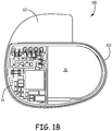
Figure 1A. Figure 1A illustrates the system including adevice 100, which is implanted subcutaneously in a pectoral region of apatient 12, and a pair ofleads 110, which are connected todevice 100.Leads 110 are shown extending distally fromdevice 100, and into the venous system ofpatient 12, so that electrodes thereof are positioned for cardiac sensing and stimulation. A terminal connector assembly of eachlead 110 is plugged into a corresponding receptacle of aninsulative housing 101 ofdevice 100, for electrical connection to device connector contacts, which are mounted within the receptacles.Figure 1A further illustratesdevice 100 including aconductive enclosure 103 to whichinsulative housing 101 is attached. With reference toFigure 1B , which is a plan view ofdevice 100 having a portion ofenclosure 103 removed,electronics 14 and an associatedpower source 16, for example, a battery assembly, are contained withinconductive enclosure 103, and a feedthrough assembly 115 (Figure 4 ), such as is known in the art, electricallycouples electronics 14 to the aforementioned connector contacts. - With further reference to
Figure 1A , the comfort ofpatient 12 may be enhanced if a volume ofdevice 100 is minimized. Yet the operational life ofdevice 100 depends, at least in part, upon the longevity ofpower source 16, which, ifpower source 16 is a battery assembly, can directly depend upon the battery cell volume thereof - the larger the volume of the battery cell, the longer the life thereof. Thus there is a need for new implantable medical device constructions that increase packaging efficiency, so that the volume of the power source may be increased without significantly increasing an overall volume of the device. Packaging arrangements for IMDs are taught inUS 2005/228456 ,US 5,814,091 andUS 2013/079600 . - The present invention provides an implantable medical device as defined in claim 1. The dependent claims define preferred embodiments. Other aspects, embodiments or methods of the present disclosure which are not covered by the appended claims do not form part of the present invention.
- The operational life of an implantable medical device, for example, a pulse generator for treating cardiac arrhythmias, may be prolonged by increasing a packaging efficiency thereof, so as to maximize the volume of a power source of the device, without significantly increasing an overall volume of the device, and without compromising reliable construction integrity. According to embodiments and methods disclosed herein, such a device includes a package formed by two conductive enclosures that are attached together, wherein the first conductive enclosure contains electronics of the device, and a second conductive enclosure, all or a portion of which is located outside the first conductive enclosure, contains a power source of the device, for example, a battery assembly, and includes an inner layer, an outer layer, and a header assembly configured to provide redundant sealing for the power source of the device.
- The inner and outer layers of the second conductive enclosure are preferably formed by separate metal sheets, which are nested one within the other, and may be in direct mechanical and electrical contact with one another, or, in some cases, electrically isolated from one another. The metal sheets for the second enclosure are preferably formed by a deep drawing method, either together or separately. The first sheet, which forms the inner layer, approximately conforms to a profile of a power source that is located therein, and the second sheet, which forms the outer layer, conforms to a profile of the first sheet. According to some embodiments, the header assembly of the second enclosure includes a header plate having a hermetically sealed feedthrough extending therethrough, wherein the feedthrough electrically couples the power source to the electronics, and wherein the header plate extends over an opening into the second enclosure, which is defined by an edge of the first sheet. The edge of the first sheet is recessed from an edge of the second sheet. The second enclosure further includes at least two welds that extend around an entire perimeter of the header plate, the first of which joins the header plate to the edge of the first sheet and provides a seal for the power source within the second enclosure, and the second of which joins the header plate to the second sheet, in proximity to the edge thereof, and provides a redundant seal for the power source.
- In some embodiments, the second enclosure includes another header plate, which also has the aforementioned feedthrough extending therethrough, and a third weld that extends around an entire perimeter of the other header plate to join the other header plate to the edge of the second sheet and to provide another redundant seal for the power source. In some additional embodiments, the first conductive enclosure comprises a metal sheet that contains the electronics, a header plate having a hermetically sealed feedthrough extending therethrough, for electrical coupling with the contained electronics, and a weld extending around an entire perimeter of the header plate of the first conductive enclosure. The sheet of the first enclosure includes an edge that defines an opening into the first enclosure, and the weld of the first enclosure joins the header plate to the edge thereof and provides a seal for the contained electronics.
- According to some embodiments, a portion of the first enclosure is inserted within a perimeter of the edge of the second sheet of the second enclosure, when the enclosures are attached together. According to some alternate embodiments, the edge of the second sheet of the second enclosure is inserted within an opening into the first enclosure, such that the edge of a sheet of the first conductive enclosure overlaps the edge of the second sheet of the second enclosure, when the enclosures are attached together. Finally, according to some embodiments and methods, an insulative housing of the device, which contains connector contacts mounted within a receptacle thereof, is secured to the first and second conductive enclosures of the device, for example, by mounting brackets, wherein a first pair of mounting brackets secures a first end of the insulative housing to the first conductive enclosure, and a second pair of mounting brackets secures a second end of the insulative housing to the second conductive enclosure.
- The following drawings are illustrative of particular embodiments of the present disclosure and therefore do not limit the scope of the invention as claimed. The drawings are not to scale (unless so stated) and are intended for use in conjunction with the explanations in the following detailed description. Embodiments will hereinafter be described in conjunction with the appended drawings wherein like numerals/letters denote like elements, and:
-
Figure 1A is a schematic of an exemplary implantable medical electrical system; -
Figure 1B is a plan view of an exemplary implantable device that may be part of the system shown inFigure 1A ; -
Figure 2A is a perspective view of an implantable medical device, according to some embodiments of the present disclosure; -
Figure 2B is an exploded perspective view of the device shown inFigure 2A , according to some embodiments; -
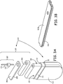
Figure 3A is an exploded perspective view of a conductive enclosure and associated power source of the device, according to some embodiments; -
Figure 3B is a perspective view of a portion of a conductive enclosure, according to some alternate embodiments; -
Figure 4 is a scaled perspective view of a portion of another implantable medical device, according to some embodiments, alongside the exemplary device ofFigures 1A-B ; -
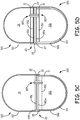
Figures 5A-D are plan views, with partial cross-section views, of portions of implantable medical devices, according to some alternate embodiments; and -
Figure 6 is a flow chart outlining some methods of the present disclosure. - The following detailed description is exemplary in nature and is not intended to limit the scope, applicability, or configuration of the invention in any way. Rather, the following description provides practical examples, and those skilled in the art will recognize that some of the examples may have suitable alternatives. Examples of constructions, materials, dimensions and fabrication processes are provided for select elements and all other elements employ that which is known by those skilled in the art.
-
Figure 2A is a perspective view of an implantablemedical device 300, according to some embodiments of the present disclosure.Figure 2A illustratesdevice 300 including a firstconductive enclosure 310, a secondconductive enclosure 320, and aninsulative housing 201. Firstconductive enclosure 310 contains electronics ofdevice 300, for example,electronics 14 shown inFigure 1B , and secondconductive enclosure 320 is attached tofirst enclosure 310 by ajunction 23, for example a welded seam that extends around an entire perimeter of bothenclosures Figure 2A further illustratesinsulative housing 201 ofdevice 300 havingreceptacles 215 formed therein, wherein connector contacts (not shown) are mounted in eachreceptacle 215 for connecting to a medical electrical lead connector, and each connector contact is coupled to the electronics contained in firstconductive enclosure 310 via a hermetically sealedfeedthrough assembly 315, which is configured according to constructions and methods known in the art. According to some preferred embodiments,insulative housing 201 is directly secured to both first andsecond enclosures mounting brackets 26, which are shown inFigure 2B . - According to embodiments of the present disclosure, second
conductive enclosure 320 is configured to contain a power source, for example, abattery assembly 316 described below, in conjunction withFigure 3A ;second enclosure 320 approximately conforms to a profile ofbattery assembly 316 to maximize the volume of the battery cell thereof within a given overall volume ofdevice 300. With reference toFigure 2B , according to some embodiments, secondconductive enclosure 320 includes a hermetically sealedfeedthrough 357 for electricallycoupling battery assembly 316 toelectronics 14.Figure 2B is an exploded perspective view ofdevice 300, according to some embodiments, wherein aheader plate 351A is shown having a hermetically sealedfeedthrough 357 extending therethrough, both of which may be part of aheader assembly 325 ofsecond enclosure 320, which is described below in conjunction withFigure 3A . -
Figure 3A is an exploded perspective view of secondconductive enclosure 320 and the associatedpower source 316, according to some embodiments.Figure 3A illustratessecond enclosure 320 including afirst metal sheet 321, which forms an inner layer ofenclosure 320, asecond metal sheet 322, which forms an outer layer ofenclosure 320, and theaforementioned header assembly 325. According to the illustrated embodiment,first sheet 321 approximately conforms to the profile ofbattery assembly 316 and includes anedge 21 that defines anopening 301 intoenclosure 320; andsecond sheet 322 conforms to a profile offirst sheet 321, preferably being in direct mechanical and electrical contact therewith. The conforming profiles ofsheets sheets Sheets - The exploded view of
Figure 3A showsbattery assembly 316 partially inserted withinenclosure 320, throughopening 301, andfirst sheet 321 partially inserted withinsecond sheet 322. With reference back toFigure 2B , according to some embodiments,header plate 351A extends overopening 301, withinedge 22 ofsecond sheet 322 and, being formed of a conductive material, such as titanium,header plate 351A is welded, around anentire perimeter 305 thereof, to both first andsecond sheets Figure 2B illustrates aweld 25 joiningheader plate 351A, around an entire perimeter thereof, tosecond sheet 322 at a location recessed fromedge 22 ofsecond sheet 322. Anotherweld 27, which may be seen inFigure 5A , extends around an entire perimeter ofheader plate 351A, joinsheader plate 351A tofirst sheet 321, and provides a seal for containedpower source 316, such thatweld 25, betweenheader plate 351A andsecond sheet 322, provides a redundant seal for containedpower source 316.Figure 3B illustrates analternative header plate 351B that includes aflange 306 extending about a perimeter thereof, and which may be substituted forheader plate 351A inheader assembly 325, according to some embodiments, for example, as illustrated inFigures 4 and5B . -
Figure 3A further illustratesheader assembly 325 including aheadspace insulator 352, which is located to extend betweenbattery assembly 316 andheader plate 351A, whenheader plate 351A extends overopening 301.Battery assembly 316 may include a battery cell formed by any suitable anode, cathode, and separator, for example, lithium, silver vanadium oxide, and polypropylene film, respectively, which are configured in any suitable manner (e.g., wound, stacked, plate or serpentine), and are contained within a non conductive liner.Headspace insulator 352 may be formed from Ethylene tetrafluoroethylene (ETFE) and configured to protectbattery assembly 316 against thermal degradation during welding operations, for example, that form welded seams, for example,junction 23, and/or welds 25, 27, and/or those which are described below. However, according to some alternate embodiments, such an insulator need not be included. - With further reference to
Figure 3A-B ,header plate 351A/351B andheadspace insulator 352 each have an aperture formed therein to receive aninsulator disk 372 offeedthrough 357, through which afeedthrough pin 371 extends.Insulator disk 372, for example, formed any suitable glass (e.g., CABAL-12, or TA-23), is hermetically sealed within the apertures and aroundfeedthrough pin 371, which may be formed from any suitable conductive material (e.g., tantalum, or niobium), according to constructions, configurations and methods that are known in the art. According to the illustrated embodiment,feedthrough pin 371 is configured to electrically couplebattery assembly 316 toelectronics 14, which are contained infirst enclosure 310, whenenclosures - With reference back to
Figures 1B and2A , if we assume thatdevice 100 anddevice 300 have approximately the same overall volume, and thatpower source 16 is a battery assembly similar tobattery assembly 316, it may be appreciated that the packaging ofbattery assembly 316 within the profile-conformingsecond enclosure 320, separate fromfirst enclosure 310, as compared to the packaging ofpower source 16 in thesame enclosure 103 withelectronics 14, can allow for an increased volume of the battery cell. For example, a volume of the battery cell ofpower source 16 may be increased from approximately 3.44 cubic centimeters (cc) to approximately 5.28 cc, when the battery cell is part ofbattery assembly 316, which is contained withinsecond enclosure 320 ofdevice 300. Given a constant packaged energy density of medium rate cells in this size range, the longevity of the battery cell increases in proportion to the volume increase, so that, in the above example, the increased packaging efficiency ofdevice 300 may givedevice 300 an increased useful life of up to approximately 50% overdevice 100. Alternately, an overall volume ofdevice 100 may be reduced without compromising battery cell longevity when the packaging ofFigures 3A-B is employed. For example, with reference toFigure 4 , an implantablemedical device 400 includes a power source/battery assembly packaged in asecond enclosure 420, in a similar fashion to the above-described packaging ofbattery assembly 316 insecond enclosure 320, such that a volume thereof, and thus the longevity, is the same as that of power source/battery assembly 16 ofdevice 100.Figure 4 is a scaled perspective view ofdevice 400 alongsidedevice 100, to illustrate the reduction in overall volume fromdevice 100 todevice 400 that is realized when the above-described packaging is employed.Figure 4 illustratesdevice 400 including afirst enclosure 410, which containselectronics 14, and asecond enclosure 420, which includes an outer layer formed by asecond metal sheet 422;second sheet 422 conforms to a profile of a first metal sheet (not shown) that forms an inner layer ofenclosure 420. Although not seen inFigure 4 , the first metal sheet, which is similar tofirst sheet 321, approximately conforms to the profile of the corresponding battery assembly, and has an edge that defines an opening intosecond enclosure 420.Figure 4 further illustratesheader plate 351B extending over the opening intosecond enclosure 420, and aweld 23B, which is formed betweenflange 306 ofheader plate 351B andsecond sheet 422, and which extends about an entire perimeter ofplate 351B, in a fashion similar to that illustrated forsecond enclosure 320 inFigure 5B . In either case described above, the dual layer construction ofsecond enclosure 320/420, via incorporation of the first and second metal sheets, facilitates redundant sealing of the corresponding battery assembly withinsecond enclosure 320/420 to maintain a reliable construction integrity fordevice 300/400. -
Figure 5A is a plan view of first and secondconductive enclosures device 300, with a partial cross-section view, according to some embodiments.Figure 5A illustratesedge 21 offirst sheet 321 recessed fromedge 22 ofsecond sheet 322, such thatedge 22 overlaps a portion of firstconductive enclosure 310 in the general location of junction 23 (e.g., the aforementioned weld).Figure 5A further illustrates the above-describedwelds header plate 351A and first andsecond sheets battery assembly 316 withinsecond enclosure 320.Figure 5B is a plan view, similar to that ofFigure 5A , in which an alternate construction includesheader plate 351B, for example, as introduced above, in conjunction withFigures 3B and4 .Figure 5B illustratesflange 306 ofheader plate 351B sandwiched betweenedge 22 ofsecond sheet 322 ofsecond enclosure 320 and anedge 11 of ametal sheet 311 of firstconductive enclosure 310, such that aweld 23A is formed betweensheet 311 andflange 306 ofheader plate 351B, about an entire perimeter thereof, and alongside the above describedweld 23B betweenflange 306 andsecond sheet 322 ofsecond enclosure 320.Sheet 311 generally conforms to a profile ofelectronics 14 contained infirst enclosure 310, and edge 11 ofsheet 311 defines an opening intofirst enclosure 310 through which the feedthrough pin offeedthrough 357 extends for coupling toelectronics 14.Figure 5B further illustrates aweld 29 formed betweenedge 21 offirst sheet 321 ofsecond enclosure 320, which is recessed fromedge 22 ofsecond sheet 322, and an edge ofheader plate 351B, which is offset fromflange 306, to joinheader plate 351B tofirst sheet 321 and to sealbattery assembly 316 within secondconductive enclosure 320, such that theaforementioned weld 23B provides a redundant seal forbattery assembly 316. -
Figure 5C is a plan view of another construction embodiment, in which the header assembly ofsecond enclosure 320 further includes anotherheader plate 451, which has an aperture through which feedthrough 357 extends.Figures 5A and5C illustrateheadspace insulator 352 positionedadjacent edge 21 offirst sheet 321, andheader plate 351A extending overheadspace insulator 352 and overedge 21 offirst sheet 321 for the above-described weld 27 (Figure 5A ) betweenheader plate 351A andfirst sheet 321. According to the embodiment ofFigure 5C ,header plate 351A extends overedge 22 ofsecond sheet 322, where anotherweld 255 is formed around an entire perimeter ofheader plate 451 to form another redundant seal forbattery assembly 316, in addition to that provided byweld 25.Figure 5C further illustratesedge 11 ofsheet 311 offirst enclosure 310 overlappingedge 22 ofsecond sheet 322 ofsecond enclosure 320 in the general area ofjunction 23. -
Figure 5D is a plan view of yet another embodiment, in which firstconductive enclosure 310 includes another header assembly, wherein the other header assembly, similar to header assembly 325 (Figure 3A ), includes aheadspace insulator 552, aheader plate 551, and afeedthrough 557 that extends through an aperture formed through each ofheadspace insulator 552 andheader plate 551.Figure 5D illustratesheadspace insulator 552 received within a perimeter ofedge 11 ofsheet 311, andheader plate 551 extending overheadspace insulator 552 and edge 11 ofsheet 311.Figure 5D further illustratesedge 22 of second sheet ofsecond enclosure 320 overlappingedge 11 ofsheet 311 offirst enclosure 311 in the region ofjunction 23. -
Figure 6 is a flow chart outlining some methods of the present disclosure for integrating a power source into an implantable medical device package, for example,battery assembly 316 into any of the above-described packages that include first and secondconductive enclosures initial step 610, metal sheets are formed for an enclosure that has an inner layer and an outer layer, for example,second enclosure 320. According to some methods, the metal sheets are placed alongside one another and then deep drawn together, according to methods known in the art, such that a first of the sheets forms the inner layer of the enclosure, and a second of the sheets forms the outer layer of the enclosure. A lubricant may be applied between the sheets to facilitate the drawing process. Alternately, the sheets may be deep drawn separately and then nested together, for example, with the aid of a lubricant. After locating a power source, such asbattery assembly 316, within the first sheet/inner layer of the enclosure, perstep 620, a feedthrough, for example, of header assembly 325 (Figure 3A ) is coupled to the power source, perstep 625, and then a header plate of the header assembly, for example,header plate step 630, such that the header plate covers an opening into the enclosure that is defined by the edge of the first sheet. According to some methods, the header plate is joined to the edge of the first sheet by laser seam welding about an entire perimeter of the header plate, after which the second sheet/outer layer of the second enclosure is nested around the first sheet/inner layer and the header plate is joined, in a similar fashion, to the second sheet, perstep 635. The weld that joins the header plate to the second sheet is located in proximity to an edge of the second sheet, and, as was described above, provides a redundant seal to that provided by the weld between the header plate and the first sheet/inner layer, for the power source located within the enclosure. Although not included inFigure 6 , according to embodiments like those described above in conjunction withFigure 5C , another header plate may be joined to second sheet/outer layer of enclosure by a third weld formed between an entire perimeter of the other header plate and the edge of the second sheet/outer layer, afterstep 635, in order to provide another redundant seal for the power source. - According to step 640, once the enclosure is redundantly sealed, per
steps electronics 14 that are located within firstconductive enclosure 310. Then, perstep 650, the two conductive enclosures are attached together, for example, by another laser seam weld atjunction 23 shown inFigure 2A . A portion of the enclosure that contains the electronics may be inserted within a perimeter of the second sheet/outer layer of the enclosure that contains the power source prior to attaching the two enclosures together, for example, resulting in the embodiment ofFigure 5A or that ofFigure 5D . Alternately, a portion of the enclosure that contains the power source is inserted within a perimeter of an edge of a sheet that forms the enclosure for the electronics, prior to attaching the two enclosures together, for example, resulting in the embodiment ofFigure 5B or that ofFigure 5C . Once the two conductive enclosures are attached together, an insulative housing, for example,housing 201, is directly secured to both enclosures, perstep 660. According to some methods, a first end ofhousing 201 is secured tofirst enclosure 310, and a second end ofhousing 201 is secured tosecond enclosure 320, each end by a pair of mounting brackets, for example, mountingbrackets 26 shown inFigure 2B , after whichelectronics 14 are coupled, via feedthrough assembly 315 (Figure 2A ), to connector contacts, which are mounted withinhousing receptacles 215. - In the foregoing detailed description, the disclosure makes reference to specific embodiments. However, it may be appreciated that various modifications and changes can be made without departing from the scope of the invention as set forth in the appended claims.
Claims (9)
- An implantable medical device (300) comprising electronics (14), a power source (316), connector contacts, a first conductive enclosure (310) containing the electronics, a second conductive enclosure (320) containing the power source, an insulative housing (201)containing the connector contacts, the first conductive enclosure including a feedthrough assembly (315) for coupling the electronics to the connector contacts, all or a portion of the second conductive enclosure being located outside the first conductive enclosure and being attached thereto, and the insulative housing including a receptacle (215) formed therein, the connector contacts being mounted in the receptacle for connecting to a medical electrical lead connector; and characterised in that the second conductive enclosure comprises:an inner layer comprising a first metal sheet (321) that approximately conforms to a profile of the power source, the first sheet including an edge (21) defining an opening (301) into the second enclosure;an outer layer comprising a second metal sheet (322) that conforms to a profile of the first sheet, the second sheet including an edge (22) adjacent to the edge of the first sheet, the edge of the first sheet being recessed from the edge of the second sheet;a header plate (351A) having a hermetically sealed feedthrough (357) extending therethrough, the header plate extending over the opening into the second enclosure, and the feedthrough electrically coupling the power source contained in the second conductive enclosure to the electronics contained in the first conductive enclosure;a first weld (25) extending around an entire perimeter of the header plate, the first weld joining the header plate to the edge of the first sheet and providing a seal for the contained power source; anda second weld (27) extending around an entire perimeter of the header plate, the second weld joining the header plate to the second sheet, in proximity to the edge thereof, and providing a redundant seal for the contained power source.
- The device of claim 1, wherein the first and second metal sheets of the second enclosure are in direct mechanical and electrical contact with one another.
- The device of any of claims 1 and 2, wherein:the first conductive enclosure comprises a metal sheet that contains the electronics, the metal sheet of the first conductive enclosure including an edge that defines an opening into the first enclosure; andthe edge of the sheet of the first conductive enclosure overlaps the edge of the second sheet of the second conductive enclosure.
- The device of any of claims 1 and 2, wherein the edge of the second sheet of the second conductive enclosure overlaps a portion of the first conductive enclosure.
- The device of any of claims 1-4, wherein the header plate of the second conductive enclosure includes a flange extending over the edge of the second sheet of the second enclosure; and the second weld joins the flange to the second sheet.
- The device of claim 5, wherein:the first conductive enclosure comprises a metal sheet that contains the electronics, the metal sheet of the first conductive enclosure including an edge that defines an opening into the first enclosure; andthe edge of the sheet of the first conductive enclosure abuts the flange of the header plate of the second conductive enclosure.
- The device of any of claims 1-6, wherein the second conductive enclosure further comprises:another header plate (351B) having the hermetically sealed feedthrough extending therethrough, the other header plate extending over the opening into the second enclosure; anda third weld extending around an entire perimeter of the other header plate, the third weld joining the other header plate to the edge of the second sheet and providing another redundant seal for the contained power source.
- The device of any of claims 1-7, wherein the first conductive enclosure comprises a metal sheet that contains the electronics, a header plate having a hermetically sealed feedthrough extending therethrough, and a weld extending around an entire perimeter of the header plate of the first conductive enclosure, the sheet of the first enclosure including an edge that defines an opening into the first enclosure, the weld of the first enclosure joining the header plate of the first enclosure to the edge thereof and providing a seal for the contained electronics, and the feedthrough of the first enclosure electrically coupling the electronics to the feedthrough of the second enclosure.
- The device of any of claims 1-8, further comprising a first pair of mounting brackets (26) and a second pair of mounting brackets (26), the first pair of mounting brackets securing a first end of the insulative housing to the first conductive enclosure, and the second pair of mounting brackets securing a second end of the insulative housing to the second conductive enclosure.
Applications Claiming Priority (3)
| Application Number | Priority Date | Filing Date | Title |
|---|---|---|---|
| US201361916486P | 2013-12-16 | 2013-12-16 | |
| US14/179,795 US9220902B2 (en) | 2013-12-16 | 2014-02-13 | Implantable medical device construction |
| PCT/US2014/068480 WO2015094673A1 (en) | 2013-12-16 | 2014-12-04 | Implantable medical device construction |
Publications (2)
| Publication Number | Publication Date |
|---|---|
| EP3082952A1 EP3082952A1 (en) | 2016-10-26 |
| EP3082952B1 true EP3082952B1 (en) | 2017-11-29 |
Family
ID=53367160
Family Applications (1)
| Application Number | Title | Priority Date | Filing Date |
|---|---|---|---|
| EP14821937.1A Active EP3082952B1 (en) | 2013-12-16 | 2014-12-04 | Implantable medical device construction |
Country Status (4)
| Country | Link |
|---|---|
| US (1) | US9220902B2 (en) |
| EP (1) | EP3082952B1 (en) |
| CN (1) | CN106029167B (en) |
| WO (1) | WO2015094673A1 (en) |
Families Citing this family (6)
| Publication number | Priority date | Publication date | Assignee | Title |
|---|---|---|---|---|
| EP3763417A1 (en) * | 2014-11-12 | 2021-01-13 | Medtronic, Inc. | Implantable medical devices with electrically isolated batteries in a separate enclosure |
| US11400301B2 (en) * | 2019-02-08 | 2022-08-02 | Cardiac Pacemakers, Inc. | Implantable medical device with reduced stress welded joint |
| US11058882B2 (en) | 2019-02-11 | 2021-07-13 | Medtronic, Inc. | Implantable medical devices having circuitry located adjacent to header-related structures |
| US11285332B2 (en) * | 2019-08-09 | 2022-03-29 | Medtronic, Inc. | Medical device housings defining a lead bore and device compartment |
| US11697027B2 (en) | 2019-10-10 | 2023-07-11 | Medtronic, Inc. | Cardiac pacing device with mechanical mode switching |
| CN113054294B (en) * | 2021-03-02 | 2023-04-07 | 清华大学 | Battery for active implanted medical instrument |
Family Cites Families (10)
| Publication number | Priority date | Publication date | Assignee | Title |
|---|---|---|---|---|
| US5573551A (en) | 1993-11-01 | 1996-11-12 | Intermedics, Inc. | Implantable medical device with detachable battery or electronic circuit |
| SE9601155D0 (en) | 1996-03-26 | 1996-03-26 | Pacesetter Ab | Device for active implant |
| US6498951B1 (en) * | 2000-10-13 | 2002-12-24 | Medtronic, Inc. | Implantable medical device employing integral housing for a formable flat battery |
| SE0201321D0 (en) | 2002-04-30 | 2002-04-30 | St Jude Medical | An implantable medical device and a manufacturing method thereof |
| US7544220B2 (en) | 2005-03-31 | 2009-06-09 | Medtronic, Inc. | Welding methods and apparatus for batteries |
| US8541131B2 (en) | 2009-05-29 | 2013-09-24 | Medtronic, Inc. | Elongate battery for implantable medical device |
| US8359098B2 (en) | 2009-05-29 | 2013-01-22 | Medtronic, Inc. | Implantable medical device with exposed generator |
| US8433409B2 (en) | 2010-01-29 | 2013-04-30 | Medtronic, Inc. | Implantable medical device battery |
| DE202010012164U1 (en) | 2010-09-03 | 2010-11-18 | Osypka, Peter, Dr.-Ing. | Battery housing for medical implants |
| US9675808B2 (en) | 2011-09-27 | 2017-06-13 | Medtronic, Inc. | Battery and capacitor arrangement for an implantable medical device |
-
2014
- 2014-02-13 US US14/179,795 patent/US9220902B2/en active Active
- 2014-12-04 CN CN201480075576.2A patent/CN106029167B/en active Active
- 2014-12-04 EP EP14821937.1A patent/EP3082952B1/en active Active
- 2014-12-04 WO PCT/US2014/068480 patent/WO2015094673A1/en not_active Ceased
Also Published As
| Publication number | Publication date |
|---|---|
| EP3082952A1 (en) | 2016-10-26 |
| US20150165196A1 (en) | 2015-06-18 |
| CN106029167A (en) | 2016-10-12 |
| CN106029167B (en) | 2019-04-12 |
| WO2015094673A1 (en) | 2015-06-25 |
| US9220902B2 (en) | 2015-12-29 |
Similar Documents
| Publication | Publication Date | Title |
|---|---|---|
| US11253711B2 (en) | Implantable energy storage device including a connection post to connect multiple electrodes | |
| US7483260B2 (en) | Dual anode capacitor with internally connected anodes | |
| US6881516B2 (en) | Contoured battery for implantable medical devices and method of manufacture | |
| US8916290B2 (en) | Contoured battery for implantable medical devices and method of manufacture | |
| US9220902B2 (en) | Implantable medical device construction | |
| US10661089B2 (en) | Electrochemical cell with adjacent cathodes | |
| US20110223464A1 (en) | Separator Systems for Batteries | |
| CA2594686A1 (en) | Electrode connector tabs | |
| WO2007090136A1 (en) | Electrochemical cell for implantable medical devices | |
| US9088012B2 (en) | Method and apparatus for a self-aligning power source casing | |
| US20100297495A1 (en) | Immobilization System For An Electrochemical Cell | |
| JPH105352A (en) | Active implantable device | |
| EP2671236B1 (en) | Hermetically sealed electrolytic capacitor | |
| US20040064163A1 (en) | Contoured battery for implantable medical devices and method of manufacture | |
| WO2007101083A2 (en) | Separator systems for electrochemical cells | |
| US7482094B2 (en) | Spacer separator subassembly | |
| US11916256B2 (en) | Battery assembly |
Legal Events
| Date | Code | Title | Description |
|---|---|---|---|
| PUAI | Public reference made under article 153(3) epc to a published international application that has entered the european phase |
Free format text: ORIGINAL CODE: 0009012 |
|
| 17P | Request for examination filed |
Effective date: 20160718 |
|
| AK | Designated contracting states |
Kind code of ref document: A1 Designated state(s): AL AT BE BG CH CY CZ DE DK EE ES FI FR GB GR HR HU IE IS IT LI LT LU LV MC MK MT NL NO PL PT RO RS SE SI SK SM TR |
|
| AX | Request for extension of the european patent |
Extension state: BA ME |
|
| DAX | Request for extension of the european patent (deleted) | ||
| RIN1 | Information on inventor provided before grant (corrected) |
Inventor name: WENGREEN, ERIC J. Inventor name: RIES, ANDREW J. Inventor name: SNYDER, TERRENCE J. Inventor name: MUNOZ, ROBERT A. Inventor name: LOVINS, JOHN E. Inventor name: LEVINA, IRYNA M. |
|
| GRAP | Despatch of communication of intention to grant a patent |
Free format text: ORIGINAL CODE: EPIDOSNIGR1 |
|
| STAA | Information on the status of an ep patent application or granted ep patent |
Free format text: STATUS: GRANT OF PATENT IS INTENDED |
|
| INTG | Intention to grant announced |
Effective date: 20170609 |
|
| GRAS | Grant fee paid |
Free format text: ORIGINAL CODE: EPIDOSNIGR3 |
|
| GRAA | (expected) grant |
Free format text: ORIGINAL CODE: 0009210 |
|
| STAA | Information on the status of an ep patent application or granted ep patent |
Free format text: STATUS: THE PATENT HAS BEEN GRANTED |
|
| AK | Designated contracting states |
Kind code of ref document: B1 Designated state(s): AL AT BE BG CH CY CZ DE DK EE ES FI FR GB GR HR HU IE IS IT LI LT LU LV MC MK MT NL NO PL PT RO RS SE SI SK SM TR |
|
| REG | Reference to a national code |
Ref country code: CH Ref legal event code: EP |
|
| REG | Reference to a national code |
Ref country code: AT Ref legal event code: REF Ref document number: 949845 Country of ref document: AT Kind code of ref document: T Effective date: 20171215 |
|
| REG | Reference to a national code |
Ref country code: IE Ref legal event code: FG4D Ref country code: FR Ref legal event code: PLFP Year of fee payment: 4 |
|
| REG | Reference to a national code |
Ref country code: DE Ref legal event code: R096 Ref document number: 602014018036 Country of ref document: DE |
|
| REG | Reference to a national code |
Ref country code: NL Ref legal event code: MP Effective date: 20171129 |
|
| REG | Reference to a national code |
Ref country code: LT Ref legal event code: MG4D |
|
| REG | Reference to a national code |
Ref country code: AT Ref legal event code: MK05 Ref document number: 949845 Country of ref document: AT Kind code of ref document: T Effective date: 20171129 |
|
| PG25 | Lapsed in a contracting state [announced via postgrant information from national office to epo] |
Ref country code: FI Free format text: LAPSE BECAUSE OF FAILURE TO SUBMIT A TRANSLATION OF THE DESCRIPTION OR TO PAY THE FEE WITHIN THE PRESCRIBED TIME-LIMIT Effective date: 20171129 Ref country code: SE Free format text: LAPSE BECAUSE OF FAILURE TO SUBMIT A TRANSLATION OF THE DESCRIPTION OR TO PAY THE FEE WITHIN THE PRESCRIBED TIME-LIMIT Effective date: 20171129 Ref country code: NO Free format text: LAPSE BECAUSE OF FAILURE TO SUBMIT A TRANSLATION OF THE DESCRIPTION OR TO PAY THE FEE WITHIN THE PRESCRIBED TIME-LIMIT Effective date: 20180228 Ref country code: ES Free format text: LAPSE BECAUSE OF FAILURE TO SUBMIT A TRANSLATION OF THE DESCRIPTION OR TO PAY THE FEE WITHIN THE PRESCRIBED TIME-LIMIT Effective date: 20171129 Ref country code: LT Free format text: LAPSE BECAUSE OF FAILURE TO SUBMIT A TRANSLATION OF THE DESCRIPTION OR TO PAY THE FEE WITHIN THE PRESCRIBED TIME-LIMIT Effective date: 20171129 |
|
| PG25 | Lapsed in a contracting state [announced via postgrant information from national office to epo] |
Ref country code: AT Free format text: LAPSE BECAUSE OF FAILURE TO SUBMIT A TRANSLATION OF THE DESCRIPTION OR TO PAY THE FEE WITHIN THE PRESCRIBED TIME-LIMIT Effective date: 20171129 Ref country code: BG Free format text: LAPSE BECAUSE OF FAILURE TO SUBMIT A TRANSLATION OF THE DESCRIPTION OR TO PAY THE FEE WITHIN THE PRESCRIBED TIME-LIMIT Effective date: 20180228 Ref country code: HR Free format text: LAPSE BECAUSE OF FAILURE TO SUBMIT A TRANSLATION OF THE DESCRIPTION OR TO PAY THE FEE WITHIN THE PRESCRIBED TIME-LIMIT Effective date: 20171129 Ref country code: LV Free format text: LAPSE BECAUSE OF FAILURE TO SUBMIT A TRANSLATION OF THE DESCRIPTION OR TO PAY THE FEE WITHIN THE PRESCRIBED TIME-LIMIT Effective date: 20171129 Ref country code: RS Free format text: LAPSE BECAUSE OF FAILURE TO SUBMIT A TRANSLATION OF THE DESCRIPTION OR TO PAY THE FEE WITHIN THE PRESCRIBED TIME-LIMIT Effective date: 20171129 Ref country code: GR Free format text: LAPSE BECAUSE OF FAILURE TO SUBMIT A TRANSLATION OF THE DESCRIPTION OR TO PAY THE FEE WITHIN THE PRESCRIBED TIME-LIMIT Effective date: 20180301 |
|
| PG25 | Lapsed in a contracting state [announced via postgrant information from national office to epo] |
Ref country code: NL Free format text: LAPSE BECAUSE OF FAILURE TO SUBMIT A TRANSLATION OF THE DESCRIPTION OR TO PAY THE FEE WITHIN THE PRESCRIBED TIME-LIMIT Effective date: 20171129 |
|
| PG25 | Lapsed in a contracting state [announced via postgrant information from national office to epo] |
Ref country code: DK Free format text: LAPSE BECAUSE OF FAILURE TO SUBMIT A TRANSLATION OF THE DESCRIPTION OR TO PAY THE FEE WITHIN THE PRESCRIBED TIME-LIMIT Effective date: 20171129 Ref country code: SK Free format text: LAPSE BECAUSE OF FAILURE TO SUBMIT A TRANSLATION OF THE DESCRIPTION OR TO PAY THE FEE WITHIN THE PRESCRIBED TIME-LIMIT Effective date: 20171129 Ref country code: EE Free format text: LAPSE BECAUSE OF FAILURE TO SUBMIT A TRANSLATION OF THE DESCRIPTION OR TO PAY THE FEE WITHIN THE PRESCRIBED TIME-LIMIT Effective date: 20171129 Ref country code: CY Free format text: LAPSE BECAUSE OF FAILURE TO SUBMIT A TRANSLATION OF THE DESCRIPTION OR TO PAY THE FEE WITHIN THE PRESCRIBED TIME-LIMIT Effective date: 20171129 Ref country code: CZ Free format text: LAPSE BECAUSE OF FAILURE TO SUBMIT A TRANSLATION OF THE DESCRIPTION OR TO PAY THE FEE WITHIN THE PRESCRIBED TIME-LIMIT Effective date: 20171129 |
|
| REG | Reference to a national code |
Ref country code: CH Ref legal event code: PL |
|
| REG | Reference to a national code |
Ref country code: DE Ref legal event code: R097 Ref document number: 602014018036 Country of ref document: DE |
|
| PG25 | Lapsed in a contracting state [announced via postgrant information from national office to epo] |
Ref country code: IT Free format text: LAPSE BECAUSE OF FAILURE TO SUBMIT A TRANSLATION OF THE DESCRIPTION OR TO PAY THE FEE WITHIN THE PRESCRIBED TIME-LIMIT Effective date: 20171129 Ref country code: PL Free format text: LAPSE BECAUSE OF FAILURE TO SUBMIT A TRANSLATION OF THE DESCRIPTION OR TO PAY THE FEE WITHIN THE PRESCRIBED TIME-LIMIT Effective date: 20171129 Ref country code: SM Free format text: LAPSE BECAUSE OF FAILURE TO SUBMIT A TRANSLATION OF THE DESCRIPTION OR TO PAY THE FEE WITHIN THE PRESCRIBED TIME-LIMIT Effective date: 20171129 |
|
| REG | Reference to a national code |
Ref country code: IE Ref legal event code: MM4A |
|
| PG25 | Lapsed in a contracting state [announced via postgrant information from national office to epo] |
Ref country code: LU Free format text: LAPSE BECAUSE OF NON-PAYMENT OF DUE FEES Effective date: 20171204 Ref country code: MT Free format text: LAPSE BECAUSE OF NON-PAYMENT OF DUE FEES Effective date: 20171204 |
|
| PLBE | No opposition filed within time limit |
Free format text: ORIGINAL CODE: 0009261 |
|
| STAA | Information on the status of an ep patent application or granted ep patent |
Free format text: STATUS: NO OPPOSITION FILED WITHIN TIME LIMIT |
|
| REG | Reference to a national code |
Ref country code: BE Ref legal event code: MM Effective date: 20171231 |
|
| PG25 | Lapsed in a contracting state [announced via postgrant information from national office to epo] |
Ref country code: IE Free format text: LAPSE BECAUSE OF NON-PAYMENT OF DUE FEES Effective date: 20171204 |
|
| 26N | No opposition filed |
Effective date: 20180830 |
|
| PG25 | Lapsed in a contracting state [announced via postgrant information from national office to epo] |
Ref country code: BE Free format text: LAPSE BECAUSE OF NON-PAYMENT OF DUE FEES Effective date: 20171231 Ref country code: SI Free format text: LAPSE BECAUSE OF FAILURE TO SUBMIT A TRANSLATION OF THE DESCRIPTION OR TO PAY THE FEE WITHIN THE PRESCRIBED TIME-LIMIT Effective date: 20171129 Ref country code: LI Free format text: LAPSE BECAUSE OF NON-PAYMENT OF DUE FEES Effective date: 20171231 Ref country code: CH Free format text: LAPSE BECAUSE OF NON-PAYMENT OF DUE FEES Effective date: 20171231 |
|
| PG25 | Lapsed in a contracting state [announced via postgrant information from national office to epo] |
Ref country code: HU Free format text: LAPSE BECAUSE OF FAILURE TO SUBMIT A TRANSLATION OF THE DESCRIPTION OR TO PAY THE FEE WITHIN THE PRESCRIBED TIME-LIMIT; INVALID AB INITIO Effective date: 20141204 Ref country code: MC Free format text: LAPSE BECAUSE OF FAILURE TO SUBMIT A TRANSLATION OF THE DESCRIPTION OR TO PAY THE FEE WITHIN THE PRESCRIBED TIME-LIMIT Effective date: 20171129 |
|
| GBPC | Gb: european patent ceased through non-payment of renewal fee |
Effective date: 20181204 |
|
| PG25 | Lapsed in a contracting state [announced via postgrant information from national office to epo] |
Ref country code: RO Free format text: LAPSE BECAUSE OF FAILURE TO SUBMIT A TRANSLATION OF THE DESCRIPTION OR TO PAY THE FEE WITHIN THE PRESCRIBED TIME-LIMIT Effective date: 20171129 |
|
| PG25 | Lapsed in a contracting state [announced via postgrant information from national office to epo] |
Ref country code: MK Free format text: LAPSE BECAUSE OF FAILURE TO SUBMIT A TRANSLATION OF THE DESCRIPTION OR TO PAY THE FEE WITHIN THE PRESCRIBED TIME-LIMIT Effective date: 20171129 |
|
| PG25 | Lapsed in a contracting state [announced via postgrant information from national office to epo] |
Ref country code: GB Free format text: LAPSE BECAUSE OF NON-PAYMENT OF DUE FEES Effective date: 20181204 |
|
| PG25 | Lapsed in a contracting state [announced via postgrant information from national office to epo] |
Ref country code: TR Free format text: LAPSE BECAUSE OF FAILURE TO SUBMIT A TRANSLATION OF THE DESCRIPTION OR TO PAY THE FEE WITHIN THE PRESCRIBED TIME-LIMIT Effective date: 20171129 |
|
| PG25 | Lapsed in a contracting state [announced via postgrant information from national office to epo] |
Ref country code: PT Free format text: LAPSE BECAUSE OF FAILURE TO SUBMIT A TRANSLATION OF THE DESCRIPTION OR TO PAY THE FEE WITHIN THE PRESCRIBED TIME-LIMIT Effective date: 20171129 |
|
| PG25 | Lapsed in a contracting state [announced via postgrant information from national office to epo] |
Ref country code: AL Free format text: LAPSE BECAUSE OF FAILURE TO SUBMIT A TRANSLATION OF THE DESCRIPTION OR TO PAY THE FEE WITHIN THE PRESCRIBED TIME-LIMIT Effective date: 20171129 Ref country code: IS Free format text: LAPSE BECAUSE OF FAILURE TO SUBMIT A TRANSLATION OF THE DESCRIPTION OR TO PAY THE FEE WITHIN THE PRESCRIBED TIME-LIMIT Effective date: 20180329 |
|
| PGFP | Annual fee paid to national office [announced via postgrant information from national office to epo] |
Ref country code: DE Payment date: 20251126 Year of fee payment: 12 |
|
| PGFP | Annual fee paid to national office [announced via postgrant information from national office to epo] |
Ref country code: FR Payment date: 20251120 Year of fee payment: 12 |