EP3081978B1 - Optical processing head - Google Patents
Optical processing head Download PDFInfo
- Publication number
- EP3081978B1 EP3081978B1 EP15785040.5A EP15785040A EP3081978B1 EP 3081978 B1 EP3081978 B1 EP 3081978B1 EP 15785040 A EP15785040 A EP 15785040A EP 3081978 B1 EP3081978 B1 EP 3081978B1
- Authority
- EP
- European Patent Office
- Prior art keywords
- lens
- optical
- optical element
- light
- processing head
- Prior art date
- Legal status (The legal status is an assumption and is not a legal conclusion. Google has not performed a legal analysis and makes no representation as to the accuracy of the status listed.)
- Active
Links
Images





Classifications
-
- B—PERFORMING OPERATIONS; TRANSPORTING
- B23—MACHINE TOOLS; METAL-WORKING NOT OTHERWISE PROVIDED FOR
- B23K—SOLDERING OR UNSOLDERING; WELDING; CLADDING OR PLATING BY SOLDERING OR WELDING; CUTTING BY APPLYING HEAT LOCALLY, e.g. FLAME CUTTING; WORKING BY LASER BEAM
- B23K26/00—Working by laser beam, e.g. welding, cutting or boring
- B23K26/02—Positioning or observing the workpiece, e.g. with respect to the point of impact; Aligning, aiming or focusing the laser beam
- B23K26/06—Shaping the laser beam, e.g. by masks or multi-focusing
- B23K26/064—Shaping the laser beam, e.g. by masks or multi-focusing by means of optical elements, e.g. lenses, mirrors or prisms
- B23K26/0648—Shaping the laser beam, e.g. by masks or multi-focusing by means of optical elements, e.g. lenses, mirrors or prisms comprising lenses
-
- B—PERFORMING OPERATIONS; TRANSPORTING
- B23—MACHINE TOOLS; METAL-WORKING NOT OTHERWISE PROVIDED FOR
- B23K—SOLDERING OR UNSOLDERING; WELDING; CLADDING OR PLATING BY SOLDERING OR WELDING; CUTTING BY APPLYING HEAT LOCALLY, e.g. FLAME CUTTING; WORKING BY LASER BEAM
- B23K26/00—Working by laser beam, e.g. welding, cutting or boring
- B23K26/02—Positioning or observing the workpiece, e.g. with respect to the point of impact; Aligning, aiming or focusing the laser beam
- B23K26/06—Shaping the laser beam, e.g. by masks or multi-focusing
- B23K26/0665—Shaping the laser beam, e.g. by masks or multi-focusing by beam condensation on the workpiece, e.g. for focusing
-
- B—PERFORMING OPERATIONS; TRANSPORTING
- B23—MACHINE TOOLS; METAL-WORKING NOT OTHERWISE PROVIDED FOR
- B23K—SOLDERING OR UNSOLDERING; WELDING; CLADDING OR PLATING BY SOLDERING OR WELDING; CUTTING BY APPLYING HEAT LOCALLY, e.g. FLAME CUTTING; WORKING BY LASER BEAM
- B23K26/00—Working by laser beam, e.g. welding, cutting or boring
- B23K26/34—Laser welding for purposes other than joining
- B23K26/342—Build-up welding
-
- G—PHYSICS
- G02—OPTICS
- G02B—OPTICAL ELEMENTS, SYSTEMS OR APPARATUS
- G02B27/00—Optical systems or apparatus not provided for by any of the groups G02B1/00 - G02B26/00, G02B30/00
- G02B27/09—Beam shaping, e.g. changing the cross-sectional area, not otherwise provided for
- G02B27/0927—Systems for changing the beam intensity distribution, e.g. Gaussian to top-hat
-
- G—PHYSICS
- G02—OPTICS
- G02B—OPTICAL ELEMENTS, SYSTEMS OR APPARATUS
- G02B27/00—Optical systems or apparatus not provided for by any of the groups G02B1/00 - G02B26/00, G02B30/00
- G02B27/09—Beam shaping, e.g. changing the cross-sectional area, not otherwise provided for
- G02B27/0938—Using specific optical elements
- G02B27/095—Refractive optical elements
- G02B27/0955—Lenses
-
- G—PHYSICS
- G02—OPTICS
- G02B—OPTICAL ELEMENTS, SYSTEMS OR APPARATUS
- G02B27/00—Optical systems or apparatus not provided for by any of the groups G02B1/00 - G02B26/00, G02B30/00
- G02B27/30—Collimators
-
- G—PHYSICS
- G02—OPTICS
- G02B—OPTICAL ELEMENTS, SYSTEMS OR APPARATUS
- G02B27/00—Optical systems or apparatus not provided for by any of the groups G02B1/00 - G02B26/00, G02B30/00
- G02B27/40—Optical focusing aids
Definitions
- the present invention relates to an optical processing head according to the preamble of claim 1, the features of which are disclosed in document EP 1 568 436 A1 .
- document US 2006/0245084 discloses an apparatus that temporarily condenses and diverges a beam inside the apparatus, and then condenses it again at a processing position.
- Document US 6 526 089 B discloses a laser marker including a collimator lens converting laser light emitted from a broad area semiconductor laser into substantially parallel beams of light, a cylindrical concave lens permitting to pass therethrough the laser light having passed through the collimator lens and being perpendicular to a plane of an active layer of the semiconductor laser, the cylindrical concave lens serving as a concave lens for the laser light having passed through the collimator lens and being parallel to the plane of the active layer, a cylindrical convex lens permitting to pass therethrough the laser light having passed through the concave lens and being perpendicular to the plane of the active layer of the semiconductor laser, the cylindrical convex lens serving as a convex lens for the laser light having passed through the collimator lens and being parallel to the plane of the active layer, and a focusing lens focusing the laser light having passed through the cylindrical convex lens.
- Document EP 1 684 109 A1 discloses a laser condensing optical system which includes a laser beam source which emits a laser beam, a condensing optical system which is arranged between the laser beam source and a medium and condenses the laser beam in the medium, and a laser divergence point moving unit which can move the position of a laser divergence point of the laser beam along an optical axis of the laser beam in accordance with the refractive index of the medium in which the laser beam is desired to be condensed and the distance from a surface of the medium to a position where the beam is desired to be condensed.
- the apparatus internally has a condensing point. If dust exists inside the apparatus, many beams are absorbed at the condensing point, increasing the energy loss.
- the present invention enables to provide a technique of solving the above-described problem.
- the present invention provides an optical processing head as defined in claim 1.
- the energy loss at the time of optical processing can be reduced.
- FIG. 1 is a view in which the optical system of the optical processing head 100 is extracted. As shown in Fig. 1 , the optical processing head 100 includes optical elements 101 to 104.
- the optical element 101 (first optical element) converts light 111 emitted by a light source into parallel light 112 (first parallel light).
- the optical element 102 (second optical element) is arranged downstream of the optical element 101, and converts the parallel light 112 into divergent light 113 (first divergent light).
- the optical element 103 (third optical element) is arranged downstream of the optical element 102, and converts the divergent light 113 into parallel light 114 (second parallel light).
- the optical element 104 (fourth optical element) is arranged downstream of the optical element 103, and converts the parallel light 114 into convergent light 115 that is condensed toward a processing surface 120.
- optical processing using such an optical system are overlay welding and three-dimensional shaping, but the optical processing is not limited to them.
- the relative arrangement of the optical elements 101 to 104 is not limited to the arrangement in Fig. 1 , and an arrangement complying with the types of optical elements (combination of lenses, mirrors, and the like) can be adopted.
- the optical elements 101 to 104 may be lenses, diffraction elements, or mirrors, but are not limited to them.
- the lens may be a planoconvex lens, a biconvex lens, an aspherical lens, or another lens.
- FIG. 2 is a view showing the internal arrangement of the optical processing head 200.
- the optical processing head 200 includes a condensing optical system apparatus 201, an observation apparatus 202, and a nozzle 203.
- a beam 205 that has been emitted by a light source (not shown) and guided from an incident end 212 to the optical processing head 200 through a light transmission portion 210 passes through the inside of the optical processing head 200 and comes out to a processing surface 260.
- the condensing optical system apparatus 201 receives supply of a processing material and gas from a material supply device and gas supply device (neither is shown) through a material supply portion 230 and a gas supply portion 240, and ejects a material 250 mixed in a processing gas to the processing surface 260 from the nozzle 203.
- the observation apparatus 202 is a device for observing the status of processing by the condensing optical system apparatus 201 from a viewpoint along the optical axis, and includes an image capturing device 221 including an image sensor such as a CCD or CMOS sensor. Light traveling from the processing surface 260 is guided to the image capturing device 221 by a half mirror 222 arranged inside the condensing optical system apparatus 201. By performing feedback control of processing parameters in accordance with the observed processing status, the processing accuracy can be improved.
- Fig. 3 is a view showing the lens arrangement of an optical system 300 inside the optical processing head 200 according to the invention.
- the optical system 300 of the optical processing head 200 includes lenses 301 to 304 as optical elements.
- the lens is smaller in absorption loss than other kinds of optical elements and higher in energy efficiency.
- the reflection loss of light can be reduced to several % or less, and the energy efficiency can be further improved. Since the absorption loss is small, the temperature hardly rises, and the thermal lens effect by the temperature rise (deformation of the lens shape by heat and degradation of the lens characteristic by a change of the refractive index) and degradation of the whole optical processing head 200 can be prevented.
- the planoconvex lens 301 is a spherical lens having a convex surface on the downstream side, and converts emitted light 311 incoming from the incident end 212 into parallel light 312.
- the planoconcave lens 302 is a spherical lens having a concave surface on the downstream side, is arranged downstream of the planoconvex lens 301, and converts the parallel light 312 into divergent light 313.
- the planoconcave lens 302 operates to cancel aberration generated by the three remaining lenses. That is, the aberration of the whole optical system 300 can be reduced.
- the planoconvex lens 303 is a spherical lens having a convex surface on the downstream side, is arranged downstream of the planoconcave lens 302, and converts the divergent light 313 into parallel light 314 larger in diameter than the parallel light 312. Hence, the density of beams can be decreased, and the temperature rise of the convex lenses 303 and 304 caused by absorption of the parallel light 314 can be reduced.
- the planoconvex lens 304 is a spherical lens having a convex surface on the upstream side, is arranged downstream of the planoconvex lens 303, and converts the parallel light 314 into convergent light 315 that is condensed toward the processing surface 260. That is, the angle formed by the beam direction of the beam 314 and the optical axis becomes equal to or smaller than the divergent angle of the divergent light 313 thanks to the presence of the planoconvex lens 303.
- the above-described half mirror 222 is interposed between the planoconvex lens 303 and the planoconvex lens 304.
- the half mirror 222 is arranged with an inclination of, for example, 45° with respect to the optical axis.
- the half mirror 222 undergoes surface treatment so as to reflect, toward the image capturing device, light of a visible light component reflected by the processing surface 260 while transmitting light emitted by the light source. Hence, the processing surface can be observed without interrupting light emitted by the light source.
- a planoconvex lens is a lens in which one of two facing surfaces is a flat surface and the other is a convex surface.
- a planoconcave lens is a lens in which one of two facing surfaces is a flat surface and the other is a concave surface.
- a spherical lens is a lens having a shape in which a convex surface or concave surface conforms to a single spherical surface.
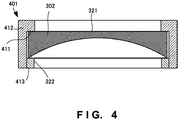
- the planoconcave lens 302 is accommodated in a lens holder 401.
- the lens holder 401 is constituted by a female holder 412 and a male holder 413, and the female holder 412 and the male holder 413 are threaded and fixed by a screw.
- the planoconcave lens 302 is fixed by a pressure, an edge 322 of the planoconcave lens 302 on the concave surface side only slightly contacts the male holder 413. That is, the interface heat resistance at this contact portion is high.
- a flat surface 321 of the planoconcave lens 302 contacts an inner flat surface 411 of the female holder 412, and the interface heat resistance is smaller than that on the concave surface side.
- the interface heat resistance decreases, the performance of dissipating heat generated by absorption of light is enhanced, and an increase in absorption by the thermal lens effect (deformation of the lens shape by heat and degradation of the lens characteristic by a change of the refractive index) can be suppressed.
- f1 is the focal length of the planoconvex lens 301
- f2 is the focal length of the planoconcave lens 302
- f3 is the focal length of the planoconvex lens 303
- f4 is the focal length of the planoconvex lens 304
- m is the enlargement magnification of the whole optical system 300.
- the condensed spot diameter needs to be decreased.
- aberration fluctuation of a beam at a condensing point
- the minimum value of the condensed spot diameter is called a best focus spot diameter.
- the best focus spot diameter is calculated by multiplying the diameter of the incident end 212 by the enlargement magnification m of the whole optical system 300. As aberration (fluctuation of a beam at a condensing point) is smaller at the time of focusing, the condensed spot becomes smaller and high-definition processing becomes possible.
- the half mirror 222 When the half mirror 222 is arranged in the optical system 300, a beam is disturbed at the time of passing through the half mirror 222, and aberration increases. To minimize the disturbance of a beam, it suffices to make a beam passing through the half mirror 222 close to light as parallel as possible.
- the half mirror 222 is interposed between the planoconvex lens 303 and the planoconvex lens 304.
- the best focus spot diameter can be minimized by arranging the planoconcave lens 302 so that the beam 314 passing through the half mirror 222 at the time of best focusing becomes parallel light.
- the planoconcave lens 302 having a focal length equal to or smaller than that of the planoconvex lens 303 is selected, and the planoconcave lens 302 and the planoconvex lens 303 are arranged so that the upstream virtual image focus of the planoconcave lens 302 and the upstream focus of the planoconvex lens 303 coincide with each other.
- the virtual image focus position (position spaced apart by f2 on the upstream side from the planoconcave lens 302) of the planoconcave lens 302, and a focus position (position spaced apart by f3 on the upstream side from the planoconvex lens 303) when parallel light enters the planoconvex lens 303 from the downstream side need to coincide with each other. Since a beam travels from the upstream side to the downstream side, the above-described focus position with respect to the planoconvex lens 303 is a virtual image focus position.
- the focal length f2 of the planoconcave lens 302 and the focal length f3 of the planoconvex lens 303 need to satisfy the following condition: f 2 / f 3 ⁇ 1
- the virtual image condensing point position of the planoconcave lens 302 and the focus position of the planoconvex lens 303 can coincide with each other. Accordingly, the energy loss can be suppressed without actually arranging a condensing point inside the apparatus.
- This arrangement also has an effect capable of decreasing the entire length of the optical system because the virtual image condensing point is positioned upstream of the planoconcave lens 302, and no real condensing point need be formed.
- the second term of this equation takes a negative value. This is the characteristic of a concave lens, and the presence of this term can decrease the total value. If a convex lens is used instead of the concave lens, the second term becomes positive, and the overall aberration becomes large. That is, this embodiment can minimize aberration by using the concave lens as the second optical element.
- the planoconcave lens 302 is a spherical lens having a concave surface on the downstream side, is arranged downstream of the planoconvex lens 301, and converts the parallel light 312 into the divergent light 313. Since the planoconcave lens 302 has the concave surface on the downstream side, the absolute value of the second term becomes maximum. That is, the effect of canceling another term becomes maximum. This produces an effect capable of minimizing aberration.
- ⁇ 4 ⁇ 2 ⁇ 0.272 ⁇ f 1 ⁇ 1.069 0.272 f 4 2 m 2 f 3 2 f 2 + f 4 2 m 2 f 3 2 f 3 + 1 m 2 f 4
- Fig. 5 shows the relationship of relation (6).
- An abscissa 501 indicates fl/f4, and an ordinate 502 indicates f3/f4.
- a curve 503 indicates the relationship between fl/f4 and f3/f4 when the enlargement magnification is 0.5.
- a curve 504 indicates the relationship between fl/f4 and f3/f4 when the enlargement magnification is 1.
- a curve 505 indicates the relationship between fl/f4 and f3/f4 when the enlargement magnification is 2. According to relation (6), aberration can be minimized if f3/f4 exists on the lower side (negative direction along the ordinate) with respect to the plotted line.
- the optical system according to this embodiment therefore has an effect in which the enlargement magnification is small and a high-definition processing apparatus can be easily designed.
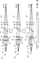
- the planoconcave lens 302 is arranged to be movable along the optical axis.
- the planoconcave lens 302 can slide along a slide mechanism 607.
- the slide mechanism 607 supports the planoconcave lens 302 so that the planoconcave lens 302 can slide along the optical axis.
- the slide of the planoconcave lens 302 may be performed manually or using a driving mechanism such as a motor.
- a control unit (not shown) may automatically control the position of the planoconcave lens 302 in accordance with the defocus value.
- the planoconcave lens 302 is slid to the upstream side to decrease the condensed spot diameter, as represented by 601 in Fig. 6 . At this time, as aberration is smaller, the condensed spot becomes smaller and the definition becomes higher.
- planoconcave lens 302 is moved so that the virtual image focus position (position spaced apart by f2 on the upstream side from the concave lens) of the planoconcave lens 302 coincides with the focus position (position spaced apart by f3 from the second convex lens) when parallel light enters the planoconvex lens 303 from the downstream side.
- defocusing By gradually sliding the planoconcave lens 302 toward the downstream side, defocusing (increasing the condensed spot diameter on the processing surface 260) can be performed, as represented by 602 and 603 in Fig. 6 . If the processing width is optimized by defocusing during processing, the processing accuracy and processing speed can be increased.
- the condensed spot diameter can be increased by about 15 times of a condensed spot diameter at the time of focusing (for example, when the condensed spot diameter at the time of focusing is 0.2 mm, the condensed spot diameter becomes 3 mm).
- the beam that has been the parallel light 314 at the time of focusing becomes divergent light 614.
- the diameter of the planoconvex lens 304 is set to be large so that a beam does not fall outside the planoconvex lens 304.
- F# (f-number) of the convergent light 315 coming out of the planoconvex lens 304 falls within the range of about 4.5 or more.
- planoconcave lens 302 is moved here, the present invention is limited to this and the planoconvex lens 303 may be moved. That is, it is only necessary to change the distance between the planoconcave lens 302 and the planoconvex lens 303 on the optical axis.
- Fig. 7 is a flowchart for explaining movement control of the planoconcave lens 302 when performing defocusing.
- the movement control is performed using a control device (not shown).
- step S701 when the condensed spot diameter (to be referred to as a defocus value) is input to the control device, it is determined in step S702 whether the input condensed spot diameter is larger than the current condensed spot diameter, that is, whether to increase the defocus value. If it is determined to increase the defocus value, the planoconcave lens 302 is moved to the downstream side (S703). If it is determined not to increase the defocus value, the process advances to step S704 to determine whether the input defocus value is smaller than the current value, that is, whether to decrease the defocus value. If it is determined to decrease the defocus value, the planoconcave lens 302 is moved to the upstream side (S705). If it is determined not to change the defocus value, the process ends without doing anything.
- the input condensed spot diameter is larger than the current condensed spot diameter, that is, whether to increase the defocus value. If it is determined to increase the defocus value, the planoconcave lens 302 is moved to the downstream side
- the embodiment can provide an optical processing head with a small energy loss by a simple optical arrangement.
- the optical processing head can also be downsized. Further, defocusing can be implemented very easily.
- FIG. 8 is a view for explaining the optical system of the optical processing head 800 according to this example.
- the optical processing head 800 according to the third example is different from the second example in which the planoconvex lenses 301, 303, and 304 are replaced by parabolic mirrors 801, 803, and 804, and the overall layout is changed in accordance with the optical path.
- the remaining arrangement and operation are the same as those in the second example, so the same reference numerals denote the same arrangement and operation and a detailed description thereof will not be repeated.
- the parabolic mirror 801 is a parabolic mirror having a focus at an incident end 212, and converts emitted light 811 incoming from the incident end 212 into parallel light 812.
- a planoconcave lens 802 is arranged downstream of the parabolic mirror 801, and converts the parallel light 812 into divergent light 813.
- the planoconcave lens 802 operates to cancel aberration of the overall optical system of the optical processing head 800. That is, the planoconcave lens 802 can decrease aberration of the overall optical system.
- the planoconcave lens 802 can slide to a position corresponding to the defocus value along the optical axis (direction of an arrow shown in Fig. 8 ).
- the optical processing head 800 includes a support portion at which the planoconcave lens 802 is supported slidably.
- the parabolic mirror 803 is arranged downstream of the planoconcave lens 802, and converts the divergent light 813 into parallel light 814.
- the parabolic mirror 803 is a parabolic mirror having a focus at the same position as the virtual image focus position of the planoconcave lens 802 arranged at a predetermined position. That is, the focal length of the parabolic mirror 803 is larger than that of the planoconcave lens 802.
- the parabolic mirror 804 is a parabolic mirror having a focus on a processing surface.
- the parabolic mirror 804 is arranged downstream of the parabolic mirror 803, and converts the parallel light 814 into convergent light 815 that is condensed on the side of a processing surface 260.
- a half mirror 222 described above is preferably interposed between the parabolic mirrors 803 and 804.
- the half mirror 222 is arranged with an inclination of, for example, 45° with respect to the optical axis. While transmitting light emitted by a light source, the half mirror 222 reflects, toward an image capturing device (not shown), light of a visible light component that has been reflected by the processing surface 260 and further reflected by the parabolic mirror 804. As a result, the processing surface 260 can be observed.
- the third example can constitute the optical processing head by using the optical system including the parabolic mirrors 801, 803, and 804 and the planoconcave lens 802. Since all the optical elements (parabolic mirrors) need not be arranged on the optical axis on a straight line, unlike the second example the degree of freedom of the layout can be increased.
- the third example uses the planoconcave lens 802, a convex mirror having a virtual image focus can also be used instead.
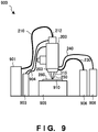
- the optical machining apparatus 900 is an apparatus that includes one of the optical processing heads 100, 200, and 800 explained in the above-described examples, and generates a three-dimensional shaped object (or overlay welding) by melting a material by heat generated by condensed light.
- the optical machining apparatus 900 including an optical processing head 200 will be explained as an example.
- the optical machining apparatus 900 includes a light source 901, a light transmitting portion 210, a coolant supply device 903, a coolant supply portion 904, a stage 905, a material supply device 906, a material supply portion 230, a gas supply device 908, and a gas supply portion 240.
- the light source 901 can be a laser, an LED, a halogen lamp, a xenon lamp, an incandescent lamp, or the like.
- the wavelength of a beam is, for example, 1,060 nm, but is not limited to this.
- the light transmitting portion 210 is, for example, an optical fiber having a core diameter of ⁇ 0.01 to 1 mm, and guides light generated by the light source 901 to the optical processing head 200.
- the core diameter of the light transmitting portion 210 serves as the diameter of an incident end 212.
- the coolant supply device 903 stores, for example, water as a coolant, and supplies the coolant by a pump to the coolant supply portion 904.
- the coolant supply portion 904 is a resin or metal hose having an inner diameter of ⁇ 2 to 6.
- the coolant is supplied into the optical processing head 200, circulated inside it, and returned to the coolant supply device 903, thereby suppressing the temperature rise of the optical processing head 200.
- the coolant supply amount is, for example, 1 to 10 L/min.
- the stage 905 is, for example, an X stage, an X-Y stage, or an X-Y-Z stage, and can operate the respective axes (X, Y, and Z).
- the material supply device 906 supplies a material to the nozzle 203 via the material supply portion 230. Examples of the material are a metal particle, a resin particle, a metal wire, and a resin wire.
- the material supply device 906 can simultaneously supply even a carrier gas.
- the material supply portion 230 is, for example, a resin or metal hose, and guides, to the nozzle 203, a particulate flow prepared by mixing a material in a carrier gas. However, when the material is a wire, no carrier gas is necessary.
- the nozzle 203 ejects a material toward a processing surface 260.
- the gas supply device 908 supplies a purge gas to the optical processing head 200 through the gas supply portion 240.
- the purge gas is, for example, nitrogen, argon, or helium. However, the purge gas is not limited to this and may also be another gas as long as the purge gas is an inert gas.
- the purge gas supplied to the optical processing head 200 is ejected from the nozzle 203 along the above-described beam.
- the optical machining apparatus 900 includes an orientation control mechanism and position control mechanism that control the orientation and position of the optical processing head 200.
- a shaped object 910 is created on the stage 905.
- Light 315 emitted by the optical processing head 200 is condensed to the processing surface 260 on the shaped object 910.
- the temperature of the processing surface 260 is raised by the condensed light, and the processing surface 260 is molten. This molted portion is called a molten pool.
- the material 250 is ejected from the nozzle 203 to the molten pool of the processing surface 260.
- the material 250 is molten into the molten pool. After that, the molten pool is cooled and hardened to deposit the material on the processing surface 260, implementing three-dimensional shaping.
- the purge gas is ejected from the nozzle 203 to the processing surface 260.
- the peripheral environment of the molten pool is purged by the purge gas.
- an oxygen-free inert gas as the purge gas, oxidization of the processing surface 260 can be prevented.
- the optical processing head 200 is cooled by the coolant supplied from the coolant supply device 903 through the coolant supply portion 904, suppressing the temperature rise during processing.
- this apparatus can implement overlay welding or three-dimensional shaping.
- the present invention is applicable to a system including a plurality of devices or a single apparatus.
- the present invention is also applicable even when a control program for implementing the functions of the embodiments is supplied to the system or apparatus directly or from a remote site.
Landscapes
- Physics & Mathematics (AREA)
- Optics & Photonics (AREA)
- Engineering & Computer Science (AREA)
- General Physics & Mathematics (AREA)
- Plasma & Fusion (AREA)
- Mechanical Engineering (AREA)
- Lenses (AREA)
- Laser Beam Processing (AREA)
Description
- The present invention relates to an optical processing head according to the preamble of
claim 1, the features of which are disclosed indocument EP 1 568 436 A1 . - In the above technical field, document
US 2006/0245084 discloses an apparatus that temporarily condenses and diverges a beam inside the apparatus, and then condenses it again at a processing position. - Document
US 6 526 089 B discloses a laser marker including a collimator lens converting laser light emitted from a broad area semiconductor laser into substantially parallel beams of light, a cylindrical concave lens permitting to pass therethrough the laser light having passed through the collimator lens and being perpendicular to a plane of an active layer of the semiconductor laser, the cylindrical concave lens serving as a concave lens for the laser light having passed through the collimator lens and being parallel to the plane of the active layer, a cylindrical convex lens permitting to pass therethrough the laser light having passed through the concave lens and being perpendicular to the plane of the active layer of the semiconductor laser, the cylindrical convex lens serving as a convex lens for the laser light having passed through the collimator lens and being parallel to the plane of the active layer, and a focusing lens focusing the laser light having passed through the cylindrical convex lens. -
Document EP 1 684 109 A1 discloses a laser condensing optical system which includes a laser beam source which emits a laser beam, a condensing optical system which is arranged between the laser beam source and a medium and condenses the laser beam in the medium, and a laser divergence point moving unit which can move the position of a laser divergence point of the laser beam along an optical axis of the laser beam in accordance with the refractive index of the medium in which the laser beam is desired to be condensed and the distance from a surface of the medium to a position where the beam is desired to be condensed. - In the technique described in this literature, the apparatus internally has a condensing point. If dust exists inside the apparatus, many beams are absorbed at the condensing point, increasing the energy loss.
- The present invention enables to provide a technique of solving the above-described problem.
- The present invention provides an optical processing head as defined in
claim 1. - According to the present invention, the energy loss at the time of optical processing can be reduced.
-
-
Fig. 1 is a view showing the arrangement of the optical system of an optical processing head according to the first example not being part of the present invention; -
Fig. 2 is a view showing the overall arrangement of an optical processing head according to the second example not being part of the present invention; -
Fig. 3 is a view showing the arrangement of the optical system of the optical processing head according to the present invention; -
Fig. 4 is a view showing the arrangement of a concave lens used in the optical processing head according to the present invention; -
Fig. 5 is a graph showing the relationship between the enlargement magnification and the design parameter allowable range in the optical processing head according to the present invention; -
Fig. 6 is a view showing movement control of the concave lens suitable to be used in the optical processing head according to the present invention; -
Fig. 7 is a flowchart showing movement control of the concave lens suitable to be used in the optical processing head of the present invention; -
Fig. 8 is a view showing the arrangement of the optical system of an optical processing head according to the third example not being part of the present invention; and -
Fig. 9 is a view showing the overall arrangement of an optical machining apparatus according to the fourth example not being part of the present invention. - A preferred embodiment of the present invention will now be described in detail with reference to the drawings. It should be noted that the relative arrangement of the components, the numerical expressions and numerical values set forth: in this embodiment do not limit the scope of the present invention unless it is specifically stated otherwise.
- An
optical processing head 100 according to a first example not being part of the present invention will be described with reference toFig. 1. Fig. 1 is a view in which the optical system of theoptical processing head 100 is extracted. As shown inFig. 1 , theoptical processing head 100 includesoptical elements 101 to 104. - The optical element 101 (first optical element) converts
light 111 emitted by a light source into parallel light 112 (first parallel light). The optical element 102 (second optical element) is arranged downstream of theoptical element 101, and converts theparallel light 112 into divergent light 113 (first divergent light). The optical element 103 (third optical element) is arranged downstream of theoptical element 102, and converts thedivergent light 113 into parallel light 114 (second parallel light). The optical element 104 (fourth optical element) is arranged downstream of theoptical element 103, and converts theparallel light 114 intoconvergent light 115 that is condensed toward aprocessing surface 120. - Examples of optical processing using such an optical system are overlay welding and three-dimensional shaping, but the optical processing is not limited to them. The relative arrangement of the
optical elements 101 to 104 is not limited to the arrangement inFig. 1 , and an arrangement complying with the types of optical elements (combination of lenses, mirrors, and the like) can be adopted. Theoptical elements 101 to 104 may be lenses, diffraction elements, or mirrors, but are not limited to them. In particular, the lens may be a planoconvex lens, a biconvex lens, an aspherical lens, or another lens. - With this arrangement, light emitted by the light source can be condensed on the processing surface without forming a condensing point inside the optical processing head. Thus, the energy loss of optical processing can be reduced.
- An
optical processing head 200 according to a second example not being part of the present invention will be described with reference toFig. 2. Fig. 2 is a view showing the internal arrangement of theoptical processing head 200. As shown inFig. 2 , theoptical processing head 200 includes a condensingoptical system apparatus 201, anobservation apparatus 202, and anozzle 203. - A
beam 205 that has been emitted by a light source (not shown) and guided from anincident end 212 to theoptical processing head 200 through alight transmission portion 210 passes through the inside of theoptical processing head 200 and comes out to aprocessing surface 260. - The condensing
optical system apparatus 201 receives supply of a processing material and gas from a material supply device and gas supply device (neither is shown) through amaterial supply portion 230 and agas supply portion 240, and ejects amaterial 250 mixed in a processing gas to theprocessing surface 260 from thenozzle 203. - The
observation apparatus 202 is a device for observing the status of processing by the condensingoptical system apparatus 201 from a viewpoint along the optical axis, and includes an image capturingdevice 221 including an image sensor such as a CCD or CMOS sensor. Light traveling from theprocessing surface 260 is guided to the image capturingdevice 221 by ahalf mirror 222 arranged inside the condensingoptical system apparatus 201. By performing feedback control of processing parameters in accordance with the observed processing status, the processing accuracy can be improved. -
Fig. 3 is a view showing the lens arrangement of anoptical system 300 inside theoptical processing head 200 according to the invention. Theoptical system 300 of theoptical processing head 200 includeslenses 301 to 304 as optical elements. The lens is smaller in absorption loss than other kinds of optical elements and higher in energy efficiency. By coating the lens with an antireflection film, the reflection loss of light can be reduced to several % or less, and the energy efficiency can be further improved. Since the absorption loss is small, the temperature hardly rises, and the thermal lens effect by the temperature rise (deformation of the lens shape by heat and degradation of the lens characteristic by a change of the refractive index) and degradation of the wholeoptical processing head 200 can be prevented. - Of the four lenses of the
optical system 300, theplanoconvex lens 301 is a spherical lens having a convex surface on the downstream side, and converts emittedlight 311 incoming from theincident end 212 intoparallel light 312. - The
planoconcave lens 302 is a spherical lens having a concave surface on the downstream side, is arranged downstream of theplanoconvex lens 301, and converts theparallel light 312 intodivergent light 313. The planoconcavelens 302 operates to cancel aberration generated by the three remaining lenses. That is, the aberration of the wholeoptical system 300 can be reduced. - The
planoconvex lens 303 is a spherical lens having a convex surface on the downstream side, is arranged downstream of theplanoconcave lens 302, and converts thedivergent light 313 intoparallel light 314 larger in diameter than theparallel light 312. Hence, the density of beams can be decreased, and the temperature rise of theconvex lenses parallel light 314 can be reduced. Theplanoconvex lens 304 is a spherical lens having a convex surface on the upstream side, is arranged downstream of theplanoconvex lens 303, and converts theparallel light 314 intoconvergent light 315 that is condensed toward theprocessing surface 260. That is, the angle formed by the beam direction of thebeam 314 and the optical axis becomes equal to or smaller than the divergent angle of thedivergent light 313 thanks to the presence of theplanoconvex lens 303. - The above-described
half mirror 222 is interposed between theplanoconvex lens 303 and theplanoconvex lens 304. Thehalf mirror 222 is arranged with an inclination of, for example, 45° with respect to the optical axis. Thehalf mirror 222 undergoes surface treatment so as to reflect, toward the image capturing device, light of a visible light component reflected by theprocessing surface 260 while transmitting light emitted by the light source. Hence, the processing surface can be observed without interrupting light emitted by the light source. - A planoconvex lens is a lens in which one of two facing surfaces is a flat surface and the other is a convex surface. A planoconcave lens is a lens in which one of two facing surfaces is a flat surface and the other is a concave surface. A spherical lens is a lens having a shape in which a convex surface or concave surface conforms to a single spherical surface.
- In general, when the lens surface is not a spherical surface but a flat surface, the processing accuracy of the surface roughness becomes high, the fabrication becomes easy, and the cost becomes low. As shown in
Fig. 4 , theplanoconcave lens 302 is accommodated in alens holder 401. Thelens holder 401 is constituted by afemale holder 412 and amale holder 413, and thefemale holder 412 and themale holder 413 are threaded and fixed by a screw. Although theplanoconcave lens 302 is fixed by a pressure, anedge 322 of theplanoconcave lens 302 on the concave surface side only slightly contacts themale holder 413. That is, the interface heat resistance at this contact portion is high. In contrast, aflat surface 321 of theplanoconcave lens 302 contacts an innerflat surface 411 of thefemale holder 412, and the interface heat resistance is smaller than that on the concave surface side. Similarly, since the planoconvex lens has a flat surface, the interface heat resistance decreases, the performance of dissipating heat generated by absorption of light is enhanced, and an increase in absorption by the thermal lens effect (deformation of the lens shape by heat and degradation of the lens characteristic by a change of the refractive index) can be suppressed. - Since the
flat surface 321 and the innerflat surface 411 of thelens holder 401 contact each other, a positional error when assembling theplanoconcave lens 302 into thelens holder 401 is small. As a result, the alignment accuracy of theplanoconcave lens 302 is increased, and aberration at a condensed spot is reduced. - f1 is the focal length of the
planoconvex lens 301, f2 is the focal length of theplanoconcave lens 302, f3 is the focal length of theplanoconvex lens 303, f4 is the focal length of theplanoconvex lens 304, and m is the enlargement magnification of the wholeoptical system 300. - To perform high-definition processing, the condensed spot diameter needs to be decreased. To decrease the condensed spot diameter, aberration (fluctuation of a beam at a condensing point) needs to be minimized. The minimum value of the condensed spot diameter is called a best focus spot diameter. The best focus spot diameter is calculated by multiplying the diameter of the
incident end 212 by the enlargement magnification m of the wholeoptical system 300. As aberration (fluctuation of a beam at a condensing point) is smaller at the time of focusing, the condensed spot becomes smaller and high-definition processing becomes possible. - When the
half mirror 222 is arranged in theoptical system 300, a beam is disturbed at the time of passing through thehalf mirror 222, and aberration increases. To minimize the disturbance of a beam, it suffices to make a beam passing through thehalf mirror 222 close to light as parallel as possible. Thehalf mirror 222 is interposed between theplanoconvex lens 303 and theplanoconvex lens 304. The best focus spot diameter can be minimized by arranging theplanoconcave lens 302 so that thebeam 314 passing through thehalf mirror 222 at the time of best focusing becomes parallel light. More specifically, to implement this, theplanoconcave lens 302 having a focal length equal to or smaller than that of theplanoconvex lens 303 is selected, and theplanoconcave lens 302 and theplanoconvex lens 303 are arranged so that the upstream virtual image focus of theplanoconcave lens 302 and the upstream focus of theplanoconvex lens 303 coincide with each other. That is, the virtual image focus position (position spaced apart by f2 on the upstream side from the planoconcave lens 302) of theplanoconcave lens 302, and a focus position (position spaced apart by f3 on the upstream side from the planoconvex lens 303) when parallel light enters theplanoconvex lens 303 from the downstream side need to coincide with each other. Since a beam travels from the upstream side to the downstream side, the above-described focus position with respect to theplanoconvex lens 303 is a virtual image focus position. - As is apparent from the above description, the focal length f2 of the
planoconcave lens 302 and the focal length f3 of theplanoconvex lens 303 need to satisfy the following condition:
- That is, by selecting the
planoconcave lens 302 and theplanoconvex lens 303 so as to satisfy f2 ≤ f3, the virtual image condensing point position of theplanoconcave lens 302 and the focus position of theplanoconvex lens 303 can coincide with each other. Accordingly, the energy loss can be suppressed without actually arranging a condensing point inside the apparatus. This arrangement also has an effect capable of decreasing the entire length of the optical system because the virtual image condensing point is positioned upstream of theplanoconcave lens 302, and no real condensing point need be formed. - As described above, to minimize the best focus spot diameter at the time of best focusing, aberration needs to be minimized. Aberration contains several components, and spherical aberration is a main component. Therefore, a condition to minimize the longitudinal component (component of spherical aberration in the optical axis direction) of spherical aberration will be examined.
- Letting f1# be the f-number of the
planoconvex lens 301, f2# be the f-number of theplanoconcave lens 302, f3# be the f-number of theplanoconvex lens 303, and f4# be the f-number of theplanoconvex lens 304, spherical aberration δ of theoptical system 300 is given by:
- Note that the second term of this equation takes a negative value. This is the characteristic of a concave lens, and the presence of this term can decrease the total value. If a convex lens is used instead of the concave lens, the second term becomes positive, and the overall aberration becomes large. That is, this embodiment can minimize aberration by using the concave lens as the second optical element.
- The
planoconcave lens 302 is a spherical lens having a concave surface on the downstream side, is arranged downstream of theplanoconvex lens 301, and converts theparallel light 312 into thedivergent light 313. Since theplanoconcave lens 302 has the concave surface on the downstream side, the absolute value of the second term becomes maximum. That is, the effect of canceling another term becomes maximum. This produces an effect capable of minimizing aberration. - Let α be the incident NA (Numerical Aperture) from the
incident end 212, β be the exit NA from theplanoconvex lens 304, and m be the enlargement magnification. Then, when the Helmholtz-Lagrange conservation law is used for α and β, equation (3) is established:
- From this, when aberration is minimum, that is, δ is 0, the following relation can be derived:


-
Fig. 5 shows the relationship of relation (6). Anabscissa 501 indicates fl/f4, and anordinate 502 indicates f3/f4. InFig. 5 , acurve 503 indicates the relationship between fl/f4 and f3/f4 when the enlargement magnification is 0.5. Acurve 504 indicates the relationship between fl/f4 and f3/f4 when the enlargement magnification is 1. Further, acurve 505 indicates the relationship between fl/f4 and f3/f4 when the enlargement magnification is 2. According to relation (6), aberration can be minimized if f3/f4 exists on the lower side (negative direction along the ordinate) with respect to the plotted line. - As is apparent from
Fig. 5 , as the enlargement magnification is smaller, the curve is positioned more upward, and the area on the lower side of the curve becomes larger. That is, the design parameter range is widened. The optical system according to this embodiment therefore has an effect in which the enlargement magnification is small and a high-definition processing apparatus can be easily designed. - The above-described arrangement is applied to lenses each simultaneously having a spherical surface and a flat surface. Such a planoconvex spherical lens or planoconcave spherical lens is lower in cost than an aspherical surface. Since all the lenses have flat surfaces, this produces an effect in which aberration caused by a positional error or aberration caused by the thermal lens effect hardly occurs.
- As shown in
Fig. 6 , theplanoconcave lens 302 is arranged to be movable along the optical axis. For example, theplanoconcave lens 302 can slide along aslide mechanism 607. More specifically, theslide mechanism 607 supports theplanoconcave lens 302 so that theplanoconcave lens 302 can slide along the optical axis. The slide of theplanoconcave lens 302 may be performed manually or using a driving mechanism such as a motor. A control unit (not shown) may automatically control the position of theplanoconcave lens 302 in accordance with the defocus value. - When performing high-definition processing, the
planoconcave lens 302 is slid to the upstream side to decrease the condensed spot diameter, as represented by 601 inFig. 6 . At this time, as aberration is smaller, the condensed spot becomes smaller and the definition becomes higher. - Thus, the
planoconcave lens 302 is moved so that the virtual image focus position (position spaced apart by f2 on the upstream side from the concave lens) of theplanoconcave lens 302 coincides with the focus position (position spaced apart by f3 from the second convex lens) when parallel light enters theplanoconvex lens 303 from the downstream side. - By gradually sliding the
planoconcave lens 302 toward the downstream side, defocusing (increasing the condensed spot diameter on the processing surface 260) can be performed, as represented by 602 and 603 inFig. 6 . If the processing width is optimized by defocusing during processing, the processing accuracy and processing speed can be increased. - When the differential distance of the planoconcave lens 302 (moving distance of the
planoconcave lens 302 when the position at the time of focusing is set as the reference) is 10 mm, the condensed spot diameter can be increased by about 15 times of a condensed spot diameter at the time of focusing (for example, when the condensed spot diameter at the time of focusing is 0.2 mm, the condensed spot diameter becomes 3 mm). In 603, the beam that has been theparallel light 314 at the time of focusing becomesdivergent light 614. At this time, the diameter of theplanoconvex lens 304 is set to be large so that a beam does not fall outside theplanoconvex lens 304. At the time of defocusing, F# (f-number) of theconvergent light 315 coming out of theplanoconvex lens 304 falls within the range of about 4.5 or more. - As described above, satisfactory defocusing can be applied even with the diameter of a compact lens. Although the
planoconcave lens 302 is moved here, the present invention is limited to this and theplanoconvex lens 303 may be moved. That is, it is only necessary to change the distance between theplanoconcave lens 302 and theplanoconvex lens 303 on the optical axis. -
Fig. 7 is a flowchart for explaining movement control of theplanoconcave lens 302 when performing defocusing. The movement control is performed using a control device (not shown). - First, in step S701, when the condensed spot diameter (to be referred to as a defocus value) is input to the control device, it is determined in step S702 whether the input condensed spot diameter is larger than the current condensed spot diameter, that is, whether to increase the defocus value. If it is determined to increase the defocus value, the
planoconcave lens 302 is moved to the downstream side (S703). If it is determined not to increase the defocus value, the process advances to step S704 to determine whether the input defocus value is smaller than the current value, that is, whether to decrease the defocus value. If it is determined to decrease the defocus value, theplanoconcave lens 302 is moved to the upstream side (S705). If it is determined not to change the defocus value, the process ends without doing anything. - As described above, the embodiment can provide an optical processing head with a small energy loss by a simple optical arrangement. The optical processing head can also be downsized. Further, defocusing can be implemented very easily.
- An
optical processing head 800 according a third example not being part of the present invention will be described with reference toFig. 8. Fig. 8 is a view for explaining the optical system of theoptical processing head 800 according to this example. Theoptical processing head 800 according to the third example is different from the second example in which theplanoconvex lenses parabolic mirrors - The
parabolic mirror 801 is a parabolic mirror having a focus at anincident end 212, and converts emitted light 811 incoming from theincident end 212 intoparallel light 812. - A
planoconcave lens 802 is arranged downstream of theparabolic mirror 801, and converts theparallel light 812 intodivergent light 813. Theplanoconcave lens 802 operates to cancel aberration of the overall optical system of theoptical processing head 800. That is, theplanoconcave lens 802 can decrease aberration of the overall optical system. Theplanoconcave lens 802 can slide to a position corresponding to the defocus value along the optical axis (direction of an arrow shown inFig. 8 ). Although not shown, theoptical processing head 800 includes a support portion at which theplanoconcave lens 802 is supported slidably. - The
parabolic mirror 803 is arranged downstream of theplanoconcave lens 802, and converts thedivergent light 813 intoparallel light 814. Theparabolic mirror 803 is a parabolic mirror having a focus at the same position as the virtual image focus position of theplanoconcave lens 802 arranged at a predetermined position. That is, the focal length of theparabolic mirror 803 is larger than that of theplanoconcave lens 802. - The
parabolic mirror 804 is a parabolic mirror having a focus on a processing surface. Theparabolic mirror 804 is arranged downstream of theparabolic mirror 803, and converts theparallel light 814 into convergent light 815 that is condensed on the side of aprocessing surface 260. - Although not shown, a
half mirror 222 described above is preferably interposed between theparabolic mirrors half mirror 222 is arranged with an inclination of, for example, 45° with respect to the optical axis. While transmitting light emitted by a light source, thehalf mirror 222 reflects, toward an image capturing device (not shown), light of a visible light component that has been reflected by theprocessing surface 260 and further reflected by theparabolic mirror 804. As a result, theprocessing surface 260 can be observed. - As described above, the third example can constitute the optical processing head by using the optical system including the
parabolic mirrors planoconcave lens 802. Since all the optical elements (parabolic mirrors) need not be arranged on the optical axis on a straight line, unlike the second example the degree of freedom of the layout can be increased. Although the third example uses theplanoconcave lens 802, a convex mirror having a virtual image focus can also be used instead. - An
optical machining apparatus 900 according a fourth example not being part of the present invention will be described with reference toFig. 9 . Theoptical machining apparatus 900 is an apparatus that includes one of the optical processing heads 100, 200, and 800 explained in the above-described examples, and generates a three-dimensional shaped object (or overlay welding) by melting a material by heat generated by condensed light. Here, theoptical machining apparatus 900 including anoptical processing head 200 will be explained as an example. - In addition to the
optical processing head 200, theoptical machining apparatus 900 includes alight source 901, alight transmitting portion 210, acoolant supply device 903, acoolant supply portion 904, astage 905, amaterial supply device 906, amaterial supply portion 230, agas supply device 908, and agas supply portion 240. - The
light source 901 can be a laser, an LED, a halogen lamp, a xenon lamp, an incandescent lamp, or the like. The wavelength of a beam is, for example, 1,060 nm, but is not limited to this. - The
light transmitting portion 210 is, for example, an optical fiber having a core diameter of φ0.01 to 1 mm, and guides light generated by thelight source 901 to theoptical processing head 200. The core diameter of thelight transmitting portion 210 serves as the diameter of anincident end 212. - The
coolant supply device 903 stores, for example, water as a coolant, and supplies the coolant by a pump to thecoolant supply portion 904. - The
coolant supply portion 904 is a resin or metal hose having an inner diameter of φ2 to 6. The coolant is supplied into theoptical processing head 200, circulated inside it, and returned to thecoolant supply device 903, thereby suppressing the temperature rise of theoptical processing head 200. The coolant supply amount is, for example, 1 to 10 L/min. - The
stage 905 is, for example, an X stage, an X-Y stage, or an X-Y-Z stage, and can operate the respective axes (X, Y, and Z). Thematerial supply device 906 supplies a material to thenozzle 203 via thematerial supply portion 230. Examples of the material are a metal particle, a resin particle, a metal wire, and a resin wire. Thematerial supply device 906 can simultaneously supply even a carrier gas. - The
material supply portion 230 is, for example, a resin or metal hose, and guides, to thenozzle 203, a particulate flow prepared by mixing a material in a carrier gas. However, when the material is a wire, no carrier gas is necessary. Thenozzle 203 ejects a material toward aprocessing surface 260. - The
gas supply device 908 supplies a purge gas to theoptical processing head 200 through thegas supply portion 240. The purge gas is, for example, nitrogen, argon, or helium. However, the purge gas is not limited to this and may also be another gas as long as the purge gas is an inert gas. The purge gas supplied to theoptical processing head 200 is ejected from thenozzle 203 along the above-described beam. - Although not shown, the
optical machining apparatus 900 includes an orientation control mechanism and position control mechanism that control the orientation and position of theoptical processing head 200. - Next, the operation of the
optical machining apparatus 900 will be explained. Ashaped object 910 is created on thestage 905. -
Light 315 emitted by theoptical processing head 200 is condensed to theprocessing surface 260 on the shapedobject 910. The temperature of theprocessing surface 260 is raised by the condensed light, and theprocessing surface 260 is molten. This molted portion is called a molten pool. - The
material 250 is ejected from thenozzle 203 to the molten pool of theprocessing surface 260. Thematerial 250 is molten into the molten pool. After that, the molten pool is cooled and hardened to deposit the material on theprocessing surface 260, implementing three-dimensional shaping. - The purge gas is ejected from the
nozzle 203 to theprocessing surface 260. Thus, the peripheral environment of the molten pool is purged by the purge gas. By selecting an oxygen-free inert gas as the purge gas, oxidization of theprocessing surface 260 can be prevented. - The
optical processing head 200 is cooled by the coolant supplied from thecoolant supply device 903 through thecoolant supply portion 904, suppressing the temperature rise during processing. - By scanning the
optical processing head 200 along theprocessing surface 260 at the same time as the above-described series of operations, desired shaping can be performed while depositing the material. That is, this apparatus can implement overlay welding or three-dimensional shaping. - The present invention is applicable to a system including a plurality of devices or a single apparatus. The present invention is also applicable even when a control program for implementing the functions of the embodiments is supplied to the system or apparatus directly or from a remote site.
Claims (5)
- An optical processing head (100, 300) comprising:a first optical element (101, 301) that is a planoconvex lens having a convex surface on a downstream side and converts light (111, 311) emitted by a light source into first parallel light (112, 312);a second optical element (102, 302) that is a planoconcave lens having a concave surface on a downstream side, arranged downstream of said first optical element (101, 301) and converts the first parallel light (112, 312) into first divergent light (113, 313), and movable along an optical axis;a third optical element (103, 303) that is a planoconvex lens having a convex surface on a downstream side and is arranged downstream of said second optical element (102, 302) and converts the first divergent light (113, 313) into second parallel light (114, 314); anda fourth optical element (104, 304) that is a planoconvex lens having a convex surface on an upstream side, is arranged downstream of said third optical element (103, 303) and converts the second parallel light (114, 314) into convergent light (115, 315) which is condensed toward a processing surfacecharacterized in thatletting f1 be a focal length of said first optical element (101, 301), f3 be a focal length of said third optical element (103, 303), f4 be a focal length of said fourth optical element (104, 304), and m be an enlargement magnification of the optical processing head (100, 300),

- The optical processing head (100) according to claim 1, wherein said third optical element (103) is arranged to be movable along an optical axis.
- The optical processing head (100) according to claim 1, wherein
letting f2 be a focal length of said second optical element (102),
- The optical processing head (100) according to claim 1, wherein a focal length of said second optical element (102) is not larger than a focal length of said third optical element (103).
- The optical processing head (100) according to any one of claims 1 to 4, wherein said second optical element (102) and said third optical element (103) are arranged to make a virtual image focus of said second optical element (102) that receives the first parallel light, coincide with a focus of said third optical element (103) that receives the first divergent light.
Applications Claiming Priority (1)
| Application Number | Priority Date | Filing Date | Title |
|---|---|---|---|
| PCT/JP2015/054882 WO2016132554A1 (en) | 2015-02-20 | 2015-02-20 | Light machining head, light machining device, and method and program for controlling same |
Publications (3)
| Publication Number | Publication Date |
|---|---|
| EP3081978A1 EP3081978A1 (en) | 2016-10-19 |
| EP3081978A4 EP3081978A4 (en) | 2017-01-18 |
| EP3081978B1 true EP3081978B1 (en) | 2019-09-11 |
Family
ID=56689215
Family Applications (1)
| Application Number | Title | Priority Date | Filing Date |
|---|---|---|---|
| EP15785040.5A Active EP3081978B1 (en) | 2015-02-20 | 2015-02-20 | Optical processing head |
Country Status (4)
| Country | Link |
|---|---|
| US (1) | US10532427B2 (en) |
| EP (1) | EP3081978B1 (en) |
| JP (1) | JP6134862B2 (en) |
| WO (1) | WO2016132554A1 (en) |
Families Citing this family (1)
| Publication number | Priority date | Publication date | Assignee | Title |
|---|---|---|---|---|
| US12265207B2 (en) * | 2021-03-04 | 2025-04-01 | Ii-Vi Delaware, Inc. | Dynamic focus for laser processing head |
Family Cites Families (10)
| Publication number | Priority date | Publication date | Assignee | Title |
|---|---|---|---|---|
| JPH0413492A (en) * | 1990-05-02 | 1992-01-17 | Komatsu Ltd | Laser beam machine |
| JP2001100145A (en) | 1999-09-29 | 2001-04-13 | Sunx Ltd | Laser marker |
| JP3498075B2 (en) * | 2001-09-14 | 2004-02-16 | 川崎重工業株式会社 | Output head for laser welding of thin plate |
| CA2489941C (en) * | 2003-12-18 | 2012-08-14 | Comau S.P.A. | A method and device for laser welding |
| TWI348408B (en) | 2004-04-28 | 2011-09-11 | Olympus Corp | Laser processing device |
| DE502004001824D1 (en) | 2004-09-30 | 2006-11-30 | Trumpf Laser Gmbh & Co Kg | Device for focusing a laser beam |
| KR100867950B1 (en) * | 2007-04-25 | 2008-11-11 | 삼성전기주식회사 | Illumination optical apparatus |
| JP2011000600A (en) * | 2009-06-17 | 2011-01-06 | Disco Abrasive Syst Ltd | Condenser lens and laser beam machining device |
| KR100984727B1 (en) * | 2010-04-30 | 2010-10-01 | 유병소 | Method and apparatus for processing workpiece |
| JP2012148316A (en) * | 2011-01-19 | 2012-08-09 | Keyence Corp | Laser beam machining apparatus |
-
2015
- 2015-02-20 EP EP15785040.5A patent/EP3081978B1/en active Active
- 2015-02-20 JP JP2016510538A patent/JP6134862B2/en active Active
- 2015-02-20 WO PCT/JP2015/054882 patent/WO2016132554A1/en not_active Ceased
- 2015-02-20 US US14/888,582 patent/US10532427B2/en active Active
Non-Patent Citations (1)
| Title |
|---|
| "The Practical Application of Light, Vol. X (Catalog)", 1 January 2006, BARLOWORLD SCIENTIFIC, Staffondshire, U.K., article CVI MELLES GRIOT: "Aberration Balancing", pages: 1.27 - 1.28, XP055437317 * |
Also Published As
| Publication number | Publication date |
|---|---|
| US20160368087A1 (en) | 2016-12-22 |
| JPWO2016132554A1 (en) | 2017-04-27 |
| JP6134862B2 (en) | 2017-05-24 |
| EP3081978A4 (en) | 2017-01-18 |
| EP3081978A1 (en) | 2016-10-19 |
| WO2016132554A1 (en) | 2016-08-25 |
| US10532427B2 (en) | 2020-01-14 |
Similar Documents
| Publication | Publication Date | Title |
|---|---|---|
| EP3088165B1 (en) | Optical processing head, optical processing device, and optical processing method | |
| CN105364301B (en) | Laser processing device capable of switching fiber core | |
| US9625623B2 (en) | Arrangement of optical elements for focusing approximately collimated beams | |
| EP0732168B1 (en) | Method and device for focusing laser beam | |
| KR20180125564A (en) | An imaging optical system for processing a material by laser emitting means and a laser machining head | |
| EP3095549B1 (en) | Optical machining head, optical machining device, optical machining device control method, and optical machining device control program | |
| CN105980912A (en) | Optical assembly for beam shaping of a laser beam for a laser processing machine | |
| JP4350558B2 (en) | Laser beam optical system and laser processing apparatus | |
| JP6808892B2 (en) | Combined wave optics | |
| KR102675028B1 (en) | Laser processing device for hard-to-access workpieces | |
| US10532427B2 (en) | Optical processing head, optical machining apparatus, and control method and control program of optical processing head | |
| EP1700665B1 (en) | Laser apparatus | |
| JP2009134316A (en) | Laser beam optical system and laser processing apparatus | |
| Blomqvist et al. | Multi-kW laser cladding using cylindrical collimators and square-formed fibers | |
| JP7780862B2 (en) | Laser processing device, optical system of laser processing device | |
| KR102712093B1 (en) | Laser processing apparatus | |
| Wang et al. | Design of optical systems with both near-field and far-field system requirements | |
| JP7186937B1 (en) | LASER PROCESSING HEAD, LASER PROCESSING APPARATUS, AND METHOD OF MANUFACTURING METAL PRODUCT | |
| JP2009506890A (en) | Laser processing apparatus with optical aperture for peripheral field removal | |
| JP2025069547A (en) | Laser processing head and laser processing device equipped with same | |
| CN119247606A (en) | A UV laser adjustable beam expansion optical system and beam expansion lens | |
| JP2025069549A (en) | Laser processing head, laser processing apparatus including same, and method for adjusting focusing positions of first laser beam and second laser beam | |
| KR20240156414A (en) | F-theta objective lens and scanner device equipped with same | |
| JP2023107301A (en) | laser processing head | |
| JPWO2023243086A5 (en) |
Legal Events
| Date | Code | Title | Description |
|---|---|---|---|
| PUAI | Public reference made under article 153(3) epc to a published international application that has entered the european phase |
Free format text: ORIGINAL CODE: 0009012 |
|
| AK | Designated contracting states |
Kind code of ref document: A1 Designated state(s): AL AT BE BG CH CY CZ DE DK EE ES FI FR GB GR HR HU IE IS IT LI LT LU LV MC MK MT NL NO PL PT RO RS SE SI SK SM TR |
|
| AX | Request for extension of the european patent |
Extension state: BA ME |
|
| A4 | Supplementary search report drawn up and despatched |
Effective date: 20161216 |
|
| RIC1 | Information provided on ipc code assigned before grant |
Ipc: G02B 27/00 20060101AFI20161212BHEP Ipc: B23K 26/06 20140101ALI20161212BHEP Ipc: B23K 26/342 20140101ALI20161212BHEP Ipc: B22F 3/105 20060101ALI20161212BHEP Ipc: H01S 3/00 20060101ALI20161212BHEP Ipc: G02B 27/09 20060101ALI20161212BHEP Ipc: B29C 67/00 20170101ALI20161212BHEP |
|
| STAA | Information on the status of an ep patent application or granted ep patent |
Free format text: STATUS: REQUEST FOR EXAMINATION WAS MADE |
|
| 17P | Request for examination filed |
Effective date: 20161105 |
|
| RIN1 | Information on inventor provided before grant (corrected) |
Inventor name: MASUKAWA, KAZUYUKI Inventor name: OBARA, TAKASHI Inventor name: OHNO, HIROSHI Inventor name: SASAKI, YUJI Inventor name: SASAKI, MITSUO Inventor name: TSUNO, SATOSHI Inventor name: SAKAI, TETSUO |
|
| STAA | Information on the status of an ep patent application or granted ep patent |
Free format text: STATUS: EXAMINATION IS IN PROGRESS |
|
| 17Q | First examination report despatched |
Effective date: 20180122 |
|
| DAX | Request for extension of the european patent (deleted) | ||
| REG | Reference to a national code |
Ref country code: DE Ref legal event code: R079 Ref document number: 602015037872 Country of ref document: DE Free format text: PREVIOUS MAIN CLASS: G02B0027000000 Ipc: G02B0027090000 |
|
| GRAP | Despatch of communication of intention to grant a patent |
Free format text: ORIGINAL CODE: EPIDOSNIGR1 |
|
| STAA | Information on the status of an ep patent application or granted ep patent |
Free format text: STATUS: GRANT OF PATENT IS INTENDED |
|
| RIC1 | Information provided on ipc code assigned before grant |
Ipc: B23K 26/342 20140101ALI20190125BHEP Ipc: G02B 27/30 20060101ALI20190125BHEP Ipc: B23K 26/06 20140101ALI20190125BHEP Ipc: G02B 27/09 20060101AFI20190125BHEP Ipc: G02B 27/40 20060101ALI20190125BHEP |
|
| INTG | Intention to grant announced |
Effective date: 20190219 |
|
| GRAJ | Information related to disapproval of communication of intention to grant by the applicant or resumption of examination proceedings by the epo deleted |
Free format text: ORIGINAL CODE: EPIDOSDIGR1 |
|
| STAA | Information on the status of an ep patent application or granted ep patent |
Free format text: STATUS: EXAMINATION IS IN PROGRESS |
|
| GRAR | Information related to intention to grant a patent recorded |
Free format text: ORIGINAL CODE: EPIDOSNIGR71 |
|
| GRAS | Grant fee paid |
Free format text: ORIGINAL CODE: EPIDOSNIGR3 |
|
| STAA | Information on the status of an ep patent application or granted ep patent |
Free format text: STATUS: GRANT OF PATENT IS INTENDED |
|
| INTC | Intention to grant announced (deleted) | ||
| GRAA | (expected) grant |
Free format text: ORIGINAL CODE: 0009210 |
|
| STAA | Information on the status of an ep patent application or granted ep patent |
Free format text: STATUS: THE PATENT HAS BEEN GRANTED |
|
| RAP1 | Party data changed (applicant data changed or rights of an application transferred) |
Owner name: TECHNOLOGY RESEARCH ASSOCIATION FOR FUTURE ADDITIV |
|
| AK | Designated contracting states |
Kind code of ref document: B1 Designated state(s): AL AT BE BG CH CY CZ DE DK EE ES FI FR GB GR HR HU IE IS IT LI LT LU LV MC MK MT NL NO PL PT RO RS SE SI SK SM TR |
|
| INTG | Intention to grant announced |
Effective date: 20190806 |
|
| REG | Reference to a national code |
Ref country code: GB Ref legal event code: FG4D |
|
| REG | Reference to a national code |
Ref country code: CH Ref legal event code: EP |
|
| REG | Reference to a national code |
Ref country code: AT Ref legal event code: REF Ref document number: 1179195 Country of ref document: AT Kind code of ref document: T Effective date: 20190915 |
|
| REG | Reference to a national code |
Ref country code: DE Ref legal event code: R096 Ref document number: 602015037872 Country of ref document: DE Ref country code: IE Ref legal event code: FG4D |
|
| REG | Reference to a national code |
Ref country code: NL Ref legal event code: MP Effective date: 20190911 |
|
| REG | Reference to a national code |
Ref country code: LT Ref legal event code: MG4D |
|
| PG25 | Lapsed in a contracting state [announced via postgrant information from national office to epo] |
Ref country code: NO Free format text: LAPSE BECAUSE OF FAILURE TO SUBMIT A TRANSLATION OF THE DESCRIPTION OR TO PAY THE FEE WITHIN THE PRESCRIBED TIME-LIMIT Effective date: 20191211 Ref country code: BG Free format text: LAPSE BECAUSE OF FAILURE TO SUBMIT A TRANSLATION OF THE DESCRIPTION OR TO PAY THE FEE WITHIN THE PRESCRIBED TIME-LIMIT Effective date: 20191211 Ref country code: LT Free format text: LAPSE BECAUSE OF FAILURE TO SUBMIT A TRANSLATION OF THE DESCRIPTION OR TO PAY THE FEE WITHIN THE PRESCRIBED TIME-LIMIT Effective date: 20190911 Ref country code: HR Free format text: LAPSE BECAUSE OF FAILURE TO SUBMIT A TRANSLATION OF THE DESCRIPTION OR TO PAY THE FEE WITHIN THE PRESCRIBED TIME-LIMIT Effective date: 20190911 Ref country code: FI Free format text: LAPSE BECAUSE OF FAILURE TO SUBMIT A TRANSLATION OF THE DESCRIPTION OR TO PAY THE FEE WITHIN THE PRESCRIBED TIME-LIMIT Effective date: 20190911 Ref country code: SE Free format text: LAPSE BECAUSE OF FAILURE TO SUBMIT A TRANSLATION OF THE DESCRIPTION OR TO PAY THE FEE WITHIN THE PRESCRIBED TIME-LIMIT Effective date: 20190911 |
|
| PG25 | Lapsed in a contracting state [announced via postgrant information from national office to epo] |
Ref country code: ES Free format text: LAPSE BECAUSE OF FAILURE TO SUBMIT A TRANSLATION OF THE DESCRIPTION OR TO PAY THE FEE WITHIN THE PRESCRIBED TIME-LIMIT Effective date: 20190911 Ref country code: AL Free format text: LAPSE BECAUSE OF FAILURE TO SUBMIT A TRANSLATION OF THE DESCRIPTION OR TO PAY THE FEE WITHIN THE PRESCRIBED TIME-LIMIT Effective date: 20190911 Ref country code: GR Free format text: LAPSE BECAUSE OF FAILURE TO SUBMIT A TRANSLATION OF THE DESCRIPTION OR TO PAY THE FEE WITHIN THE PRESCRIBED TIME-LIMIT Effective date: 20191212 Ref country code: RS Free format text: LAPSE BECAUSE OF FAILURE TO SUBMIT A TRANSLATION OF THE DESCRIPTION OR TO PAY THE FEE WITHIN THE PRESCRIBED TIME-LIMIT Effective date: 20190911 Ref country code: LV Free format text: LAPSE BECAUSE OF FAILURE TO SUBMIT A TRANSLATION OF THE DESCRIPTION OR TO PAY THE FEE WITHIN THE PRESCRIBED TIME-LIMIT Effective date: 20190911 |
|
| REG | Reference to a national code |
Ref country code: AT Ref legal event code: MK05 Ref document number: 1179195 Country of ref document: AT Kind code of ref document: T Effective date: 20190911 |
|
| PG25 | Lapsed in a contracting state [announced via postgrant information from national office to epo] |
Ref country code: PL Free format text: LAPSE BECAUSE OF FAILURE TO SUBMIT A TRANSLATION OF THE DESCRIPTION OR TO PAY THE FEE WITHIN THE PRESCRIBED TIME-LIMIT Effective date: 20190911 Ref country code: AT Free format text: LAPSE BECAUSE OF FAILURE TO SUBMIT A TRANSLATION OF THE DESCRIPTION OR TO PAY THE FEE WITHIN THE PRESCRIBED TIME-LIMIT Effective date: 20190911 Ref country code: NL Free format text: LAPSE BECAUSE OF FAILURE TO SUBMIT A TRANSLATION OF THE DESCRIPTION OR TO PAY THE FEE WITHIN THE PRESCRIBED TIME-LIMIT Effective date: 20190911 Ref country code: EE Free format text: LAPSE BECAUSE OF FAILURE TO SUBMIT A TRANSLATION OF THE DESCRIPTION OR TO PAY THE FEE WITHIN THE PRESCRIBED TIME-LIMIT Effective date: 20190911 Ref country code: PT Free format text: LAPSE BECAUSE OF FAILURE TO SUBMIT A TRANSLATION OF THE DESCRIPTION OR TO PAY THE FEE WITHIN THE PRESCRIBED TIME-LIMIT Effective date: 20200113 Ref country code: RO Free format text: LAPSE BECAUSE OF FAILURE TO SUBMIT A TRANSLATION OF THE DESCRIPTION OR TO PAY THE FEE WITHIN THE PRESCRIBED TIME-LIMIT Effective date: 20190911 |
|
| PG25 | Lapsed in a contracting state [announced via postgrant information from national office to epo] |
Ref country code: IS Free format text: LAPSE BECAUSE OF FAILURE TO SUBMIT A TRANSLATION OF THE DESCRIPTION OR TO PAY THE FEE WITHIN THE PRESCRIBED TIME-LIMIT Effective date: 20200224 Ref country code: CZ Free format text: LAPSE BECAUSE OF FAILURE TO SUBMIT A TRANSLATION OF THE DESCRIPTION OR TO PAY THE FEE WITHIN THE PRESCRIBED TIME-LIMIT Effective date: 20190911 Ref country code: SK Free format text: LAPSE BECAUSE OF FAILURE TO SUBMIT A TRANSLATION OF THE DESCRIPTION OR TO PAY THE FEE WITHIN THE PRESCRIBED TIME-LIMIT Effective date: 20190911 Ref country code: SM Free format text: LAPSE BECAUSE OF FAILURE TO SUBMIT A TRANSLATION OF THE DESCRIPTION OR TO PAY THE FEE WITHIN THE PRESCRIBED TIME-LIMIT Effective date: 20190911 |
|
| REG | Reference to a national code |
Ref country code: DE Ref legal event code: R097 Ref document number: 602015037872 Country of ref document: DE |
|
| PLBE | No opposition filed within time limit |
Free format text: ORIGINAL CODE: 0009261 |
|
| STAA | Information on the status of an ep patent application or granted ep patent |
Free format text: STATUS: NO OPPOSITION FILED WITHIN TIME LIMIT |
|
| PG2D | Information on lapse in contracting state deleted |
Ref country code: IS |
|
| PG25 | Lapsed in a contracting state [announced via postgrant information from national office to epo] |
Ref country code: DK Free format text: LAPSE BECAUSE OF FAILURE TO SUBMIT A TRANSLATION OF THE DESCRIPTION OR TO PAY THE FEE WITHIN THE PRESCRIBED TIME-LIMIT Effective date: 20190911 Ref country code: IS Free format text: LAPSE BECAUSE OF FAILURE TO SUBMIT A TRANSLATION OF THE DESCRIPTION OR TO PAY THE FEE WITHIN THE PRESCRIBED TIME-LIMIT Effective date: 20200112 |
|
| 26N | No opposition filed |
Effective date: 20200615 |
|
| PG25 | Lapsed in a contracting state [announced via postgrant information from national office to epo] |
Ref country code: SI Free format text: LAPSE BECAUSE OF FAILURE TO SUBMIT A TRANSLATION OF THE DESCRIPTION OR TO PAY THE FEE WITHIN THE PRESCRIBED TIME-LIMIT Effective date: 20190911 |
|
| REG | Reference to a national code |
Ref country code: CH Ref legal event code: PL |
|
| GBPC | Gb: european patent ceased through non-payment of renewal fee |
Effective date: 20200220 |
|
| REG | Reference to a national code |
Ref country code: BE Ref legal event code: MM Effective date: 20200229 |
|
| PG25 | Lapsed in a contracting state [announced via postgrant information from national office to epo] |
Ref country code: LU Free format text: LAPSE BECAUSE OF NON-PAYMENT OF DUE FEES Effective date: 20200220 Ref country code: MC Free format text: LAPSE BECAUSE OF FAILURE TO SUBMIT A TRANSLATION OF THE DESCRIPTION OR TO PAY THE FEE WITHIN THE PRESCRIBED TIME-LIMIT Effective date: 20190911 |
|
| PG25 | Lapsed in a contracting state [announced via postgrant information from national office to epo] |
Ref country code: LI Free format text: LAPSE BECAUSE OF NON-PAYMENT OF DUE FEES Effective date: 20200229 Ref country code: CH Free format text: LAPSE BECAUSE OF NON-PAYMENT OF DUE FEES Effective date: 20200229 |
|
| PG25 | Lapsed in a contracting state [announced via postgrant information from national office to epo] |
Ref country code: FR Free format text: LAPSE BECAUSE OF NON-PAYMENT OF DUE FEES Effective date: 20200229 Ref country code: IE Free format text: LAPSE BECAUSE OF NON-PAYMENT OF DUE FEES Effective date: 20200220 Ref country code: GB Free format text: LAPSE BECAUSE OF NON-PAYMENT OF DUE FEES Effective date: 20200220 |
|
| PG25 | Lapsed in a contracting state [announced via postgrant information from national office to epo] |
Ref country code: BE Free format text: LAPSE BECAUSE OF NON-PAYMENT OF DUE FEES Effective date: 20200229 |
|
| PG25 | Lapsed in a contracting state [announced via postgrant information from national office to epo] |
Ref country code: IT Free format text: LAPSE BECAUSE OF NON-PAYMENT OF DUE FEES Effective date: 20200220 |
|
| PG25 | Lapsed in a contracting state [announced via postgrant information from national office to epo] |
Ref country code: TR Free format text: LAPSE BECAUSE OF FAILURE TO SUBMIT A TRANSLATION OF THE DESCRIPTION OR TO PAY THE FEE WITHIN THE PRESCRIBED TIME-LIMIT Effective date: 20190911 Ref country code: MT Free format text: LAPSE BECAUSE OF FAILURE TO SUBMIT A TRANSLATION OF THE DESCRIPTION OR TO PAY THE FEE WITHIN THE PRESCRIBED TIME-LIMIT Effective date: 20190911 Ref country code: CY Free format text: LAPSE BECAUSE OF FAILURE TO SUBMIT A TRANSLATION OF THE DESCRIPTION OR TO PAY THE FEE WITHIN THE PRESCRIBED TIME-LIMIT Effective date: 20190911 |
|
| REG | Reference to a national code |
Ref country code: DE Ref legal event code: R081 Ref document number: 602015037872 Country of ref document: DE Owner name: KABUSHIKI KAISHA TOSHIBA, JP Free format text: FORMER OWNER: TECHNOLOGY RESEARCH ASSOCIATION FOR FUTURE ADDITIVE MANUFACTURING, TOKYO, JP |
|
| PG25 | Lapsed in a contracting state [announced via postgrant information from national office to epo] |
Ref country code: MK Free format text: LAPSE BECAUSE OF FAILURE TO SUBMIT A TRANSLATION OF THE DESCRIPTION OR TO PAY THE FEE WITHIN THE PRESCRIBED TIME-LIMIT Effective date: 20190911 |
|
| PGFP | Annual fee paid to national office [announced via postgrant information from national office to epo] |
Ref country code: DE Payment date: 20251224 Year of fee payment: 12 |