EP3080832B1 - Silicon microsphere fabrication - Google Patents
Silicon microsphere fabrication Download PDFInfo
- Publication number
- EP3080832B1 EP3080832B1 EP14824210.0A EP14824210A EP3080832B1 EP 3080832 B1 EP3080832 B1 EP 3080832B1 EP 14824210 A EP14824210 A EP 14824210A EP 3080832 B1 EP3080832 B1 EP 3080832B1
- Authority
- EP
- European Patent Office
- Prior art keywords
- substrate
- silicon
- spheres
- mask layer
- ink
- Prior art date
- Legal status (The legal status is an assumption and is not a legal conclusion. Google has not performed a legal analysis and makes no representation as to the accuracy of the status listed.)
- Active
Links
Images
Classifications
-
- H—ELECTRICITY
- H10—SEMICONDUCTOR DEVICES; ELECTRIC SOLID-STATE DEVICES NOT OTHERWISE PROVIDED FOR
- H10F—INORGANIC SEMICONDUCTOR DEVICES SENSITIVE TO INFRARED RADIATION, LIGHT, ELECTROMAGNETIC RADIATION OF SHORTER WAVELENGTH OR CORPUSCULAR RADIATION
- H10F71/00—Manufacture or treatment of devices covered by this subclass
- H10F71/121—The active layers comprising only Group IV materials
-
- B—PERFORMING OPERATIONS; TRANSPORTING
- B29—WORKING OF PLASTICS; WORKING OF SUBSTANCES IN A PLASTIC STATE IN GENERAL
- B29C—SHAPING OR JOINING OF PLASTICS; SHAPING OF MATERIAL IN A PLASTIC STATE, NOT OTHERWISE PROVIDED FOR; AFTER-TREATMENT OF THE SHAPED PRODUCTS, e.g. REPAIRING
- B29C33/00—Moulds or cores; Details thereof or accessories therefor
- B29C33/38—Moulds or cores; Details thereof or accessories therefor characterised by the material or the manufacturing process
- B29C33/3842—Manufacturing moulds, e.g. shaping the mould surface by machining
-
- B—PERFORMING OPERATIONS; TRANSPORTING
- B29—WORKING OF PLASTICS; WORKING OF SUBSTANCES IN A PLASTIC STATE IN GENERAL
- B29C—SHAPING OR JOINING OF PLASTICS; SHAPING OF MATERIAL IN A PLASTIC STATE, NOT OTHERWISE PROVIDED FOR; AFTER-TREATMENT OF THE SHAPED PRODUCTS, e.g. REPAIRING
- B29C39/00—Shaping by casting, i.e. introducing the moulding material into a mould or between confining surfaces without significant moulding pressure; Apparatus therefor
- B29C39/003—Shaping by casting, i.e. introducing the moulding material into a mould or between confining surfaces without significant moulding pressure; Apparatus therefor characterised by the choice of material
-
- B—PERFORMING OPERATIONS; TRANSPORTING
- B29—WORKING OF PLASTICS; WORKING OF SUBSTANCES IN A PLASTIC STATE IN GENERAL
- B29C—SHAPING OR JOINING OF PLASTICS; SHAPING OF MATERIAL IN A PLASTIC STATE, NOT OTHERWISE PROVIDED FOR; AFTER-TREATMENT OF THE SHAPED PRODUCTS, e.g. REPAIRING
- B29C39/00—Shaping by casting, i.e. introducing the moulding material into a mould or between confining surfaces without significant moulding pressure; Apparatus therefor
- B29C39/02—Shaping by casting, i.e. introducing the moulding material into a mould or between confining surfaces without significant moulding pressure; Apparatus therefor for making articles of definite length, i.e. discrete articles
-
- B—PERFORMING OPERATIONS; TRANSPORTING
- B29—WORKING OF PLASTICS; WORKING OF SUBSTANCES IN A PLASTIC STATE IN GENERAL
- B29C—SHAPING OR JOINING OF PLASTICS; SHAPING OF MATERIAL IN A PLASTIC STATE, NOT OTHERWISE PROVIDED FOR; AFTER-TREATMENT OF THE SHAPED PRODUCTS, e.g. REPAIRING
- B29C39/00—Shaping by casting, i.e. introducing the moulding material into a mould or between confining surfaces without significant moulding pressure; Apparatus therefor
- B29C39/22—Component parts, details or accessories; Auxiliary operations
- B29C39/26—Moulds or cores
-
- B—PERFORMING OPERATIONS; TRANSPORTING
- B29—WORKING OF PLASTICS; WORKING OF SUBSTANCES IN A PLASTIC STATE IN GENERAL
- B29C—SHAPING OR JOINING OF PLASTICS; SHAPING OF MATERIAL IN A PLASTIC STATE, NOT OTHERWISE PROVIDED FOR; AFTER-TREATMENT OF THE SHAPED PRODUCTS, e.g. REPAIRING
- B29C39/00—Shaping by casting, i.e. introducing the moulding material into a mould or between confining surfaces without significant moulding pressure; Apparatus therefor
- B29C39/22—Component parts, details or accessories; Auxiliary operations
- B29C39/36—Removing moulded articles
-
- B—PERFORMING OPERATIONS; TRANSPORTING
- B29—WORKING OF PLASTICS; WORKING OF SUBSTANCES IN A PLASTIC STATE IN GENERAL
- B29C—SHAPING OR JOINING OF PLASTICS; SHAPING OF MATERIAL IN A PLASTIC STATE, NOT OTHERWISE PROVIDED FOR; AFTER-TREATMENT OF THE SHAPED PRODUCTS, e.g. REPAIRING
- B29C39/00—Shaping by casting, i.e. introducing the moulding material into a mould or between confining surfaces without significant moulding pressure; Apparatus therefor
- B29C39/22—Component parts, details or accessories; Auxiliary operations
- B29C39/38—Heating or cooling
-
- H—ELECTRICITY
- H10—SEMICONDUCTOR DEVICES; ELECTRIC SOLID-STATE DEVICES NOT OTHERWISE PROVIDED FOR
- H10F—INORGANIC SEMICONDUCTOR DEVICES SENSITIVE TO INFRARED RADIATION, LIGHT, ELECTROMAGNETIC RADIATION OF SHORTER WAVELENGTH OR CORPUSCULAR RADIATION
- H10F77/00—Constructional details of devices covered by this subclass
- H10F77/10—Semiconductor bodies
- H10F77/14—Shape of semiconductor bodies; Shapes, relative sizes or dispositions of semiconductor regions within semiconductor bodies
- H10F77/143—Shape of semiconductor bodies; Shapes, relative sizes or dispositions of semiconductor regions within semiconductor bodies comprising quantum structures
-
- H—ELECTRICITY
- H10—SEMICONDUCTOR DEVICES; ELECTRIC SOLID-STATE DEVICES NOT OTHERWISE PROVIDED FOR
- H10F—INORGANIC SEMICONDUCTOR DEVICES SENSITIVE TO INFRARED RADIATION, LIGHT, ELECTROMAGNETIC RADIATION OF SHORTER WAVELENGTH OR CORPUSCULAR RADIATION
- H10F77/00—Constructional details of devices covered by this subclass
- H10F77/10—Semiconductor bodies
- H10F77/14—Shape of semiconductor bodies; Shapes, relative sizes or dispositions of semiconductor regions within semiconductor bodies
- H10F77/147—Shapes of bodies
-
- H—ELECTRICITY
- H10—SEMICONDUCTOR DEVICES; ELECTRIC SOLID-STATE DEVICES NOT OTHERWISE PROVIDED FOR
- H10F—INORGANIC SEMICONDUCTOR DEVICES SENSITIVE TO INFRARED RADIATION, LIGHT, ELECTROMAGNETIC RADIATION OF SHORTER WAVELENGTH OR CORPUSCULAR RADIATION
- H10F77/00—Constructional details of devices covered by this subclass
- H10F77/70—Surface textures, e.g. pyramid structures
-
- B—PERFORMING OPERATIONS; TRANSPORTING
- B29—WORKING OF PLASTICS; WORKING OF SUBSTANCES IN A PLASTIC STATE IN GENERAL
- B29K—INDEXING SCHEME ASSOCIATED WITH SUBCLASSES B29B, B29C OR B29D, RELATING TO MOULDING MATERIALS OR TO MATERIALS FOR MOULDS, REINFORCEMENTS, FILLERS OR PREFORMED PARTS, e.g. INSERTS
- B29K2105/00—Condition, form or state of moulded material or of the material to be shaped
- B29K2105/0058—Liquid or visquous
- B29K2105/0064—Latex, emulsion or dispersion
-
- B—PERFORMING OPERATIONS; TRANSPORTING
- B29—WORKING OF PLASTICS; WORKING OF SUBSTANCES IN A PLASTIC STATE IN GENERAL
- B29K—INDEXING SCHEME ASSOCIATED WITH SUBCLASSES B29B, B29C OR B29D, RELATING TO MOULDING MATERIALS OR TO MATERIALS FOR MOULDS, REINFORCEMENTS, FILLERS OR PREFORMED PARTS, e.g. INSERTS
- B29K2105/00—Condition, form or state of moulded material or of the material to be shaped
- B29K2105/25—Solid
- B29K2105/251—Particles, powder or granules
-
- B—PERFORMING OPERATIONS; TRANSPORTING
- B29—WORKING OF PLASTICS; WORKING OF SUBSTANCES IN A PLASTIC STATE IN GENERAL
- B29K—INDEXING SCHEME ASSOCIATED WITH SUBCLASSES B29B, B29C OR B29D, RELATING TO MOULDING MATERIALS OR TO MATERIALS FOR MOULDS, REINFORCEMENTS, FILLERS OR PREFORMED PARTS, e.g. INSERTS
- B29K2909/00—Use of inorganic materials not provided for in groups B29K2803/00 - B29K2807/00, as mould material
- B29K2909/08—Glass
-
- B—PERFORMING OPERATIONS; TRANSPORTING
- B29—WORKING OF PLASTICS; WORKING OF SUBSTANCES IN A PLASTIC STATE IN GENERAL
- B29K—INDEXING SCHEME ASSOCIATED WITH SUBCLASSES B29B, B29C OR B29D, RELATING TO MOULDING MATERIALS OR TO MATERIALS FOR MOULDS, REINFORCEMENTS, FILLERS OR PREFORMED PARTS, e.g. INSERTS
- B29K2995/00—Properties of moulding materials, reinforcements, fillers, preformed parts or moulds
- B29K2995/0003—Properties of moulding materials, reinforcements, fillers, preformed parts or moulds having particular electrical or magnetic properties, e.g. piezoelectric
- B29K2995/0005—Conductive
-
- B—PERFORMING OPERATIONS; TRANSPORTING
- B29—WORKING OF PLASTICS; WORKING OF SUBSTANCES IN A PLASTIC STATE IN GENERAL
- B29K—INDEXING SCHEME ASSOCIATED WITH SUBCLASSES B29B, B29C OR B29D, RELATING TO MOULDING MATERIALS OR TO MATERIALS FOR MOULDS, REINFORCEMENTS, FILLERS OR PREFORMED PARTS, e.g. INSERTS
- B29K2995/00—Properties of moulding materials, reinforcements, fillers, preformed parts or moulds
- B29K2995/0037—Other properties
- B29K2995/0094—Geometrical properties
-
- B—PERFORMING OPERATIONS; TRANSPORTING
- B29—WORKING OF PLASTICS; WORKING OF SUBSTANCES IN A PLASTIC STATE IN GENERAL
- B29L—INDEXING SCHEME ASSOCIATED WITH SUBCLASS B29C, RELATING TO PARTICULAR ARTICLES
- B29L2031/00—Other particular articles
- B29L2031/34—Electrical apparatus, e.g. sparking plugs or parts thereof
- B29L2031/3406—Components, e.g. resistors
-
- H—ELECTRICITY
- H10—SEMICONDUCTOR DEVICES; ELECTRIC SOLID-STATE DEVICES NOT OTHERWISE PROVIDED FOR
- H10P—GENERIC PROCESSES OR APPARATUS FOR THE MANUFACTURE OR TREATMENT OF DEVICES COVERED BY CLASS H10
- H10P14/00—Formation of materials, e.g. in the shape of layers or pillars
- H10P14/20—Formation of materials, e.g. in the shape of layers or pillars of semiconductor materials
- H10P14/26—Formation of materials, e.g. in the shape of layers or pillars of semiconductor materials using liquid deposition
- H10P14/265—Formation of materials, e.g. in the shape of layers or pillars of semiconductor materials using liquid deposition using solutions
-
- H—ELECTRICITY
- H10—SEMICONDUCTOR DEVICES; ELECTRIC SOLID-STATE DEVICES NOT OTHERWISE PROVIDED FOR
- H10P—GENERIC PROCESSES OR APPARATUS FOR THE MANUFACTURE OR TREATMENT OF DEVICES COVERED BY CLASS H10
- H10P14/00—Formation of materials, e.g. in the shape of layers or pillars
- H10P14/20—Formation of materials, e.g. in the shape of layers or pillars of semiconductor materials
- H10P14/34—Deposited materials, e.g. layers
- H10P14/3402—Deposited materials, e.g. layers characterised by the chemical composition
- H10P14/3404—Deposited materials, e.g. layers characterised by the chemical composition being Group IVA materials
- H10P14/3411—Silicon, silicon germanium or germanium
-
- H—ELECTRICITY
- H10—SEMICONDUCTOR DEVICES; ELECTRIC SOLID-STATE DEVICES NOT OTHERWISE PROVIDED FOR
- H10P—GENERIC PROCESSES OR APPARATUS FOR THE MANUFACTURE OR TREATMENT OF DEVICES COVERED BY CLASS H10
- H10P14/00—Formation of materials, e.g. in the shape of layers or pillars
- H10P14/20—Formation of materials, e.g. in the shape of layers or pillars of semiconductor materials
- H10P14/34—Deposited materials, e.g. layers
- H10P14/3451—Structure
- H10P14/3452—Microstructure
- H10P14/3461—Nanoparticles
-
- Y—GENERAL TAGGING OF NEW TECHNOLOGICAL DEVELOPMENTS; GENERAL TAGGING OF CROSS-SECTIONAL TECHNOLOGIES SPANNING OVER SEVERAL SECTIONS OF THE IPC; TECHNICAL SUBJECTS COVERED BY FORMER USPC CROSS-REFERENCE ART COLLECTIONS [XRACs] AND DIGESTS
- Y02—TECHNOLOGIES OR APPLICATIONS FOR MITIGATION OR ADAPTATION AGAINST CLIMATE CHANGE
- Y02E—REDUCTION OF GREENHOUSE GAS [GHG] EMISSIONS, RELATED TO ENERGY GENERATION, TRANSMISSION OR DISTRIBUTION
- Y02E10/00—Energy generation through renewable energy sources
- Y02E10/50—Photovoltaic [PV] energy
- Y02E10/547—Monocrystalline silicon PV cells
-
- Y—GENERAL TAGGING OF NEW TECHNOLOGICAL DEVELOPMENTS; GENERAL TAGGING OF CROSS-SECTIONAL TECHNOLOGIES SPANNING OVER SEVERAL SECTIONS OF THE IPC; TECHNICAL SUBJECTS COVERED BY FORMER USPC CROSS-REFERENCE ART COLLECTIONS [XRACs] AND DIGESTS
- Y02—TECHNOLOGIES OR APPLICATIONS FOR MITIGATION OR ADAPTATION AGAINST CLIMATE CHANGE
- Y02P—CLIMATE CHANGE MITIGATION TECHNOLOGIES IN THE PRODUCTION OR PROCESSING OF GOODS
- Y02P70/00—Climate change mitigation technologies in the production process for final industrial or consumer products
- Y02P70/50—Manufacturing or production processes characterised by the final manufactured product
Definitions
- This invention relates to forming precision microspheres of a material and, in particular, to forming microspheres of silicon.
- United States Patent No. 5,556,791 describes a process for forming such silicon spheres by first forming a fine powder of silicon, such as by grinding bulk silicon. This dry powder is referred to as feedstock. Next, a template (a stencil) having small holes formed through it is positioned on a conveyor belt. The holes are then completely filled with the feedstock. The template is then lifted to form uniform piles of the feedstock on the conveyor belt. The piles are then heated by an optical furnace which melts the silicon powder in each pile, and the melted silicon generally forms spheres by surface tension. The spheres are then cooled. The silicon spheres are then further processed and deposited on a substrate to form a solar panel. The silicon spheres have diameters of about 30 mils (762 um).
- a known method for forming silicon spheres less than 200 um in diameter uses sieves to select milled silicon particles within a desired range of sizes, and then a high temperature plasma is used to melt the individual particles in a reducing atmosphere to spherodize the silicon (see US Patent 6,780,219 ).
- This process wastes silicon, the extreme heat of the plasma (>2000C) creates relatively defective spheres, the silicon dioxide spheres are created as a byproduct, and the process is highly energy intensive.
- Another known method forms silicon spheres of about 1 mm in diameter for solar cells.
- This process requires sieving roughly shaped silicon powder to obtain particles within a desired range, using a binder to form larger silicon granules generally the size and shape of the desired spheres by means of a tumbling granulator, and placing each individual granule in its own recess of a heating substrate.
- Conventional heating furnaces such as resistive or inductive furnaces, are then used to melt the silicon powder in each granule, and the granules form spheres.
- This process is energy intensive, requires time for a quartz substrate to react with molten silicon, requires a time-consuming process of placing individual granules in recesses, has a limited throughput of about 20,000 granules per substrate, and reduces the longevity of the substrate.
- very fine silicon powder is milled from high quality bulk silicon while the silicon is in a fluid, such as acetone, alcohol, ether, water, ethylene glycol, proplylene glycol or other liquid or combination of liquids, to create a silicon ink.
- a fluid such as acetone, alcohol, ether, water, ethylene glycol, proplylene glycol or other liquid or combination of liquids.
- the average size of the silicon particles may be from tens of nanometers to hundreds of nanometers or several microns in size, and the particles can have any shape.
- the fluid may be any suitable evaporative or volatile organic or inorganic compound. Due to the fineness of the silicon particles, the particles stay suspended in the fluid for an extended period of time, remain uniformly dispersed, and can have a high bulk density. Dispersants and/or surfactants, such as fluorosurfactants, inorganic salts, or organic salts, can be added to stabilize the dispersion for longer periods of time.
- a quartz substrate e.g., a fused silica plate
- a mask is used to define closely spaced indentations in the substrate.
- Each opening in the mask may have a diameter of about 10 um - 100 um.
- the openings may be circular, hexagonal, or other shapes.
- the substrate is then subjected to one of, or a combination of, wet and dry etching to form a large number of closely spaced indentations in the substrate with diameters around 200 um or less.
- the indentions have rounded sides and the bottom of each indentation may be rounded or flat.
- the indentations may be created using laser drilling.
- a laser is used to ablate indentations into the quartz.
- An ultraviolet or carbon dioxide laser can be used to make these indentations.
- the entire surface of the substrate is then coated with a thin film that repels the silicon ink to prevent wetting of the substrate by the silicon ink. This coating may be reapplied occasionally or even each time the substrate is reused.
- the silicon ink is then coated over the surface of the substrate to fill the indentations.
- a squeegee may be used to force the silicon ink into the indentations and remove excess ink. The excess ink is recycled.
- the volume of the silicon in each indention is substantially the same volume since the density of the silicon particles in the ink is substantially uniform.
- the ink is heated to evaporate the fluid.
- the dry silicon particles are then rapidly heated (e.g., in less than 10 ms), using a furnace, to melt the silicon particles to form precision silicon spheres by surface tension.
- An optical furnace is preferably used, in which case the light that is not absorbed by the silicon is primarily transmitted through the transparent substrate, so the silicon is selectively heated relative to the substrate. Preferential heating of the silicon is achieved so the substrate with the indentations does not react with the silicon and can be reused.
- a reflective metal layer such as aluminum
- a protective surface layer such as silicon nitride can be deposited over the quartz substrate to limit reaction with the silicon ink during melting and/or increase the longevity of the substrate.
- Pulsed radiation thermal processing a type of optical furnace, as described in US Patent 8,410,712 , may also be used to melt the silicon most efficiently.
- the power, length, and frequency of the pulse can be tuned to achieve the exact heating profile required to efficiently melt and cool the silicon.
- the substrate may also be convectively heated to reduce the peak power required by the optical furnace, which minimizes the entire energy cost of the process.
- the spheres are then rapidly cooled by removing application of the light and/or the quartz plates from the furnace.
- the processed quartz substrate is inexpensive and can be large, such as 1 square meter. Therefore, a single substrate may produce 100 million silicon spheres during a single process. The substrate is reusable.
- the quality of the spheres can be higher than the prior art's larger spheres. Higher quality includes greater crystallinity, fewer grain boundaries, and a lower concentration of impurities due to the rapid melting. Further, since the spheres are very small, the surface tension results in more precise spherical shapes, since the low weight of the silicon relative to the sphere's surface area does not compress the sphere's shape.
- the spheres may then be removed from the indentations, printed as a monolayer on a metal substrate and further processed to form diodes in a solar panel.
- Spheres of materials other than silicon may also be formed using this process.
- Fig. 1 is a cross-sectional view of a substrate 10, which may be rectangular and having a surface area of about one square meter, or any other suitable size.
- the substrate 10 can be any thickness, such as 5 mm - 1 cm.
- the substrate 10 may be fused silica or synthetic fused silica (also referred to as quartz) or other material that can withstand the heat used in the process and can be easily etched.
- the substrate 10 is substantially transparent.
- a photoresist mask 12, or soft mask is then patterned over the hard mask 11, using conventional photolithographic techniques, to form an array of openings 14, each opening having a diameter of about 10 um - 100 um, depending on the desired size of the spheres.
- Fig. 2 is a cross-sectional view of a very small portion of the substrate 10 cutting across three openings 14 in a mask 12.
- Fig. 3 is a top down view of the entire substrate 10 having the photoresist mask 12 formed over it, defining openings 14.
- the openings 14 may be arranged in a rectangular or hexagonal array, or another pattern.
- the openings 14 may be circular, hexagonal, or another shape. Closely spaced hexagonal openings arranged in a hexagonal array, resembling a honeycomb, are preferred to obtain a maximum density of openings.
- the mask 12 has as many as 100 million openings overa 1 square meter substrate 10 for forming 100 million silicon spheres during a single process flow.
- the width of each opening 14 is about 20 um prior to etching to form spheres in the range of 75-50 um, since the etchant etches the substrate 10 isotropically under the hard mask 11. Due to the large size of the substrate 10, the mask 12 may be patterned using a large-area mask or by a standard step and repeat photolithographic exposure, followed by development.
- Fig. 4 illustrates the substrate 10 undergoing a Reactive Ion Etch (RIE) etching process 13 to etch through the hard mask 11 and expose the quartz substrate 10.
- RIE Reactive Ion Etch
- the photoresist mask 12 is then stripped off by dissolving it.
- Fig. 5 illustrates the substrate 10 undergoing a wet etch, using an HF solution 15.
- the wet etching is isotropic so etches vertically and horizontally. Therefore, the depth of the resulting indentations 16 is approximately equal to the horizontal etching under the hard mask 11.
- the indentations 16 may have a rounded bottom or a flat bottom with rounded side walls. If hexagonal openings 14 are used, the wet etch still produces indentations 16 with rounded sides and a partially rounded bottom.
- the required depth of the indentations 16 is determined by the volume of silicon ink needed to create silicon spheres of a certain size. In one embodiment, the depth may be on the order of 50 um for spheres about 75 um - 50 um in diameter, depending on the density of the silicon ink.
- the indentations 16 may be created using laser drilling.
- a laser is used to ablate indentations 16 into the quartz substrate 10.
- An ultraviolet or carbon dioxide laser can be used to make the indentations 16.
- Fig. 6 illustrates the substrate 10 after removal of the hard mask 11 using a conventional etchant for amorphous silicon.
- a reflective metal layer 17, such as aluminum, may be deposited on the back of the transparent quartz substrate 10 to reflect optical energy back into the silicon during a subsequent heating step.
- the metal layer 17 may be a laminated, sputtered, printed, or deposited in other ways.
- a thin film (not shown) is then formed on the surface of the substrate 10 to prevent wetting of the surface by the silicon ink, resulting in high interfacial surface tension between the substrate and the silicon ink.
- the optimal film is dependent on the silicon ink fluid used.
- the film is a functionalized alkyl silane, which is conventionally used as a water repellant (a hydrophobic film). Many alkyl silanes are available to tune the interfacial energy.
- a silicon ink may be prepared in a number of different ways.
- bulk silicon is milled by a fine grinder, conventionally used to form powder from bulk materials.
- the average diameter of the grains may be on the order of tens of nanometers. In another embodiment, the average diameter of the grains is less than 1 um. Uniformity of the grains is not required to achieve uniformity of the silicon spheres.
- Such grinding devices are known, and suitable silicon nanoparticles may be purchased from various companies.
- the silicon powder is then mixed in a suitable fluid, such as acetone, alcohol, ether, water, ethylene glycol, propylene glycol or other liquid or semi-liquid, to create the silicon ink.
- a suitable fluid such as acetone, alcohol, ether, water, ethylene glycol, propylene glycol or other liquid or semi-liquid.
- the fluid may be any suitable evaporative or volatile organic or inorganic compound. Due to the fineness of the silicon particles, the particles stay suspended in the fluid for an extended period of time, remain uniformly dispersed, and can have a high bulk density. Dispersants and/or surfactants, such as fluorosurfactants, inorganic salts, or organic salts, can be added to stabilize the dispersion for longer periods of time.
- fluid includes any suitable liquid or semi-liquid medium at the process temperature.
- relatively large pieces of silicon, already within the fluid are milled by rotating grinding surfaces within the fluid until the silicon particles are of the desired small size.
- a wet milling process is generally described in US Patent 6,638,491 .
- the silicon ink 18, containing the silicon nanoparticles 20 is dispensed over the entire surface of the substrate 10 by spraying, printing, or by any other suitable process, to completely fill the indentations 16.
- a squeegee 22 is then passed over the surface of the substrate 10 to further urge the ink 18 into the indentations 16 and remove the excess ink 18 from the surface.
- the excess ink 18 is then recycled.
- the surface of the substrate 10 is now planar.
- the surface of the substrate 10 is subjected to a two-step heating process.
- First, the fluid part of the ink 18 is evaporated at a first heat level to cause only the silicon nanoparticles 20 to remain in the indentations 16.
- Such heating may be performed in an oven or using any other suitable heating process.
- the silicon nanoparticles 20 are melted (liquefied) in less than 30 milliseconds and form a silicon sphere 24 by surface tension (a cohesive force). It has been shown that molten silicon has a surface tension of 783.5x10 -3 N/m at 1410C (+/- 3-4%).
- the Novacentrix system comprises a heating lamp that is pulse width modulated to generate the required heating profile. The system does not substantially heat the substrate 10 since it is substantially transparent. Other suitable photonic curing systems are also commercially available from Novacentrix and other manufacturers.
- the reflective metal layer 17 ( Fig. 6 ) is used, the light passing through the substrate 10 is reflected upward to further heat the silicon nanoparticles 20.
- the power, length, and frequency of the pulse can be tuned to achieve the exact heating profile required to efficiently melt and cool the silicon.
- the substrate may also be convectively heated to reduce the peak power required by the optical furnace, which minimizes the entire energy cost of the process.
- the spheres 24 are then rapidly cooled (because of their small size) below their solidification temperature simply by removing application of the light. Active cooling may be used if decelerated cooling is desired. Accordingly, the entire volume of the silicon nanoparticles 20 contained in an indentation 16 forms a sphere 24. Since the density of the nanoparticles 20 is uniform in the ink 18, and the volume of each indentation 16 is uniform, the spheres 24 are of uniform size. Since there are many nanoparticles 20 that make up a single sphere 24, the individual differences in nanoparticle shape and size are not relevant, since the average size of the nanoparticles 20 in each indentation 16 is the same.
- Uniform spheres 24 are also created with hexagonal openings 14, since the silicon nanoparticles 20 still accumulate during melting to form a sphere by surface tension.
- any sphere size can be obtained, such as down to 20 um in diameter.
- the process forms spheres 24 with less than 5% total variance in the final sphere diameter, such as ⁇ 3.5 um with a 70 um mean diameter.
- the printing process can tolerate 10% variance in the final sphere diameter.
- the spheres 24 may be further processed by rapid melting and cooling to improve the crystallinity and bulk chemical purity of the spheres. Since the small spheres 24 can be melted and cooled very quickly, higher crystallinity and a lower impurity concentration can be achieved. Additional processes may be performed on the spheres 24, depending on the final application for the spheres 24.
- the spheres 24 may then be removed from the substrate 10 by an air knife and vacuum, or by tilting the substrate 10 while vibrating it, or by other means such as brushing, blowing, or collection in a fluid.
- the substrate 10 of Fig. 6 may be reused many times.
- the process flow may fabricate, for example, 3 square meters/minute, where each square meter produces over 100 million spheres 24.
- a typically throughput may be greater than 100 kg of silicon spheres 24 per hour.
- the conveyor belt itself may be provided with a reflective surface underlying the substrate 10 to reflect back the optical energy when heating the silicon.
- a thermal insulator layer may be added between the quartz substrate 10 and the conveyor belt to increase the thermal mass of the substrate 10. This maintains a greater temperature gradient between the silicon and the substrate 10 and can be desirable for controlled heating/cooling.
- the spheres 24 may be uniformly dispersed in another solvent system to make a silicon slurry and printed on a metal (e.g., aluminum) substrate 28 as a monolayer in the formation of a solar panel 30.
- the spheres 24 may be p-type, and their top surface may be doped n-type, after being printed on the metal substrate 28, to form pn junction diodes, with the cathodes on top and the anodes in ohmic contact with the metal substrate 28.
- a transparent conductor may be formed to contact the top cathodes of the diodes, and the transparent conductor and metal substrate 28 are electrically connected to a voltage converter.
- the process may be used for forming small spheres of other types of materials as well, such as other semiconductor materials, dielectric materials, metals, etc.
- the ink used to make the spheres may be a mixture of nanoparticles of different materials, and the resulting spheres form a substantially homogeneous alloy of the materials in the ink due to the melting of the mixture.
Landscapes
- Engineering & Computer Science (AREA)
- Manufacturing & Machinery (AREA)
- Mechanical Engineering (AREA)
- Photovoltaic Devices (AREA)
- Silicon Compounds (AREA)
Description
- This invention relates to forming precision microspheres of a material and, in particular, to forming microspheres of silicon.
- It is a known technique to form a solar panel by depositing an array of silicon spheres over a metal substrate, then processing the silicon spheres to form diodes that convert sunlight to electricity, as described in
US Patent 8,133,768 . - United States Patent No.
5,556,791 describes a process for forming such silicon spheres by first forming a fine powder of silicon, such as by grinding bulk silicon. This dry powder is referred to as feedstock. Next, a template (a stencil) having small holes formed through it is positioned on a conveyor belt. The holes are then completely filled with the feedstock. The template is then lifted to form uniform piles of the feedstock on the conveyor belt. The piles are then heated by an optical furnace which melts the silicon powder in each pile, and the melted silicon generally forms spheres by surface tension. The spheres are then cooled. The silicon spheres are then further processed and deposited on a substrate to form a solar panel. The silicon spheres have diameters of about 30 mils (762 um). DocumentUS2009/0325336 describes techniques to texture surfaces. By using smaller spheres, such as less than 200 um, as a monolayer in a solar panel, there is a very high surface area to volume ratio, making the solar panel more cost effective. It is also beneficial during processing for the spheres to have the same size and electrical characteristics. - It would be extremely difficult to form uniform silicon spheres with diameters less than 200 um using the above-described process. For example, completely and uniformly filling 200 um or smaller holes in a stencil with dry silicon powder would be very difficult due to the frictional forces involved and the variable air gaps between the particles. Although laser drilling of holes less than 200 um to form a stencil is possible, creating a stencil with a sufficiently large number of laser drilled holes in close proximity (e.g., over a million) to make the sphere fabrication cost-effective would be impractical.
- A known method for forming silicon spheres less than 200 um in diameter uses sieves to select milled silicon particles within a desired range of sizes, and then a high temperature plasma is used to melt the individual particles in a reducing atmosphere to spherodize the silicon (see
US Patent 6,780,219 ). This process wastes silicon, the extreme heat of the plasma (>2000C) creates relatively defective spheres, the silicon dioxide spheres are created as a byproduct, and the process is highly energy intensive. - Another known method, described in
EP2182555A1 , forms silicon spheres of about 1 mm in diameter for solar cells. This process requires sieving roughly shaped silicon powder to obtain particles within a desired range, using a binder to form larger silicon granules generally the size and shape of the desired spheres by means of a tumbling granulator, and placing each individual granule in its own recess of a heating substrate. Conventional heating furnaces, such as resistive or inductive furnaces, are then used to melt the silicon powder in each granule, and the granules form spheres. This process is energy intensive, requires time for a quartz substrate to react with molten silicon, requires a time-consuming process of placing individual granules in recesses, has a limited throughput of about 20,000 granules per substrate, and reduces the longevity of the substrate. - What is needed is a cost-effective method for forming precision silicon spheres having diameters less than 200 um using a heating process that does not compromise the substrate.
- In one embodiment, very fine silicon powder is milled from high quality bulk silicon while the silicon is in a fluid, such as acetone, alcohol, ether, water, ethylene glycol, proplylene glycol or other liquid or combination of liquids, to create a silicon ink. The average size of the silicon particles may be from tens of nanometers to hundreds of nanometers or several microns in size, and the particles can have any shape.
- The fluid may be any suitable evaporative or volatile organic or inorganic compound. Due to the fineness of the silicon particles, the particles stay suspended in the fluid for an extended period of time, remain uniformly dispersed, and can have a high bulk density. Dispersants and/or surfactants, such as fluorosurfactants, inorganic salts, or organic salts, can be added to stabilize the dispersion for longer periods of time.
- A quartz substrate (e.g., a fused silica plate) is prepared as follows. A mask is used to define closely spaced indentations in the substrate. Each opening in the mask may have a diameter of about 10 um - 100 um. The openings may be circular, hexagonal, or other shapes.
- The substrate is then subjected to one of, or a combination of, wet and dry etching to form a large number of closely spaced indentations in the substrate with diameters around 200 um or less. The indentions have rounded sides and the bottom of each indentation may be rounded or flat.
- Alternatively, the indentations may be created using laser drilling. In this case, a laser is used to ablate indentations into the quartz. An ultraviolet or carbon dioxide laser can be used to make these indentations. Once the indentations have been formed, the entire surface of the substrate is then coated with a thin film that repels the silicon ink to prevent wetting of the substrate by the silicon ink. This coating may be reapplied occasionally or even each time the substrate is reused.
- The silicon ink is then coated over the surface of the substrate to fill the indentations. A squeegee may be used to force the silicon ink into the indentations and remove excess ink. The excess ink is recycled. The volume of the silicon in each indention is substantially the same volume since the density of the silicon particles in the ink is substantially uniform.
- The ink is heated to evaporate the fluid. The dry silicon particles are then rapidly heated (e.g., in less than 10 ms), using a furnace, to melt the silicon particles to form precision silicon spheres by surface tension. An optical furnace is preferably used, in which case the light that is not absorbed by the silicon is primarily transmitted through the transparent substrate, so the silicon is selectively heated relative to the substrate. Preferential heating of the silicon is achieved so the substrate with the indentations does not react with the silicon and can be reused.
- Several methods can be used to increase the efficiency of the melting process to optimize the cost-effectiveness of this manufacturing process. A reflective metal layer, such as aluminum, may be added to the back of the quartz to reflect optical energy back into the silicon. A protective surface layer such as silicon nitride can be deposited over the quartz substrate to limit reaction with the silicon ink during melting and/or increase the longevity of the substrate.
- Pulsed radiation thermal processing, a type of optical furnace, as described in
US Patent 8,410,712 , may also be used to melt the silicon most efficiently. With the pulsed radiation thermal process, the power, length, and frequency of the pulse can be tuned to achieve the exact heating profile required to efficiently melt and cool the silicon. The substrate may also be convectively heated to reduce the peak power required by the optical furnace, which minimizes the entire energy cost of the process. - The spheres are then rapidly cooled by removing application of the light and/or the quartz plates from the furnace.
- Since the indentations are defined using photolithography (such as by a large-scale mask or by a step and repeat exposure process), the processed quartz substrate is inexpensive and can be large, such as 1 square meter. Therefore, a single substrate may produce 100 million silicon spheres during a single process. The substrate is reusable.
- In addition to the extremely high throughput, the quality of the spheres can be higher than the prior art's larger spheres. Higher quality includes greater crystallinity, fewer grain boundaries, and a lower concentration of impurities due to the rapid melting. Further, since the spheres are very small, the surface tension results in more precise spherical shapes, since the low weight of the silicon relative to the sphere's surface area does not compress the sphere's shape.
- The spheres may then be removed from the indentations, printed as a monolayer on a metal substrate and further processed to form diodes in a solar panel.
- Spheres of materials other than silicon may also be formed using this process.
- Other embodiments are described.
-
-
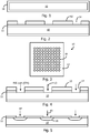
Fig. 1 is a cross-sectional view of a rectangular quartz substrate coated with amorphous silicon deposited by physical or chemical vapor deposition. -
Fig. 2 is a cross-sectional view of a small portion of the substrate ofFig. 1 after a photoresist mask has been formed, cutting across three openings in the photoresist mask, with their pitch increased for illustration. -
Fig. 3 is a top view of the quartz substrate showing the mask having an array of openings, where the openings are greatly magnified. -
Fig. 4 illustrates the substrate ofFig. 2 during RIE etching, which etches through the amorphous silicon to expose the quartz substrate. -
Fig. 5 illustrates the substrate ofFig. 4 during wet etching to form many millions of indentations in the substrate. -
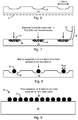
Fig. 6 illustrates the substrate ofFig. 5 after the amorphous silicon mask is removed. -
Fig. 7 illustrates the substrate ofFig. 6 after the indentations are filled with a silicon ink. -
Fig. 8 illustrates the substrate ofFig. 7 after the silicon ink is heated to evaporate the fluid and melt the silicon powder to form uniform silicon spheres down to 20 um in diameter. -
Fig. 9 is a cross-sectional view of a portion of a solar panel during fabrication showing a monolayer of the silicon spheres ofFig. 8 being printed on a metal substrate. - Elements that are the same or similar are identified with the same number.
-
Fig. 1 is a cross-sectional view of asubstrate 10, which may be rectangular and having a surface area of about one square meter, or any other suitable size. Thesubstrate 10 can be any thickness, such as 5 mm - 1 cm. Thesubstrate 10 may be fused silica or synthetic fused silica (also referred to as quartz) or other material that can withstand the heat used in the process and can be easily etched. Thesubstrate 10 is substantially transparent. - A
hard mask 11, such as amorphous silicon, is uniformly deposited over thequartz substrate 10 by physical or chemical vapor deposition. - As shown in
Fig. 2 , aphotoresist mask 12, or soft mask, is then patterned over thehard mask 11, using conventional photolithographic techniques, to form an array ofopenings 14, each opening having a diameter of about 10 um - 100 um, depending on the desired size of the spheres.Fig. 2 is a cross-sectional view of a very small portion of thesubstrate 10 cutting across threeopenings 14 in amask 12. -
Fig. 3 is a top down view of theentire substrate 10 having thephotoresist mask 12 formed over it, definingopenings 14. Theopenings 14 may be arranged in a rectangular or hexagonal array, or another pattern. Theopenings 14 may be circular, hexagonal, or another shape. Closely spaced hexagonal openings arranged in a hexagonal array, resembling a honeycomb, are preferred to obtain a maximum density of openings. In one embodiment, themask 12 has as many as 100 million openings overa 1square meter substrate 10 for forming 100 million silicon spheres during a single process flow. - In one embodiment, the width of each
opening 14 is about 20 um prior to etching to form spheres in the range of 75-50 um, since the etchant etches thesubstrate 10 isotropically under thehard mask 11. Due to the large size of thesubstrate 10, themask 12 may be patterned using a large-area mask or by a standard step and repeat photolithographic exposure, followed by development. -
Fig. 4 illustrates thesubstrate 10 undergoing a Reactive Ion Etch (RIE)etching process 13 to etch through thehard mask 11 and expose thequartz substrate 10. - The
photoresist mask 12 is then stripped off by dissolving it. -
Fig. 5 illustrates thesubstrate 10 undergoing a wet etch, using anHF solution 15. The wet etching is isotropic so etches vertically and horizontally. Therefore, the depth of the resultingindentations 16 is approximately equal to the horizontal etching under thehard mask 11. - Depending on the width of the
openings 14, theindentations 16 may have a rounded bottom or a flat bottom with rounded side walls. Ifhexagonal openings 14 are used, the wet etch still producesindentations 16 with rounded sides and a partially rounded bottom. The required depth of theindentations 16 is determined by the volume of silicon ink needed to create silicon spheres of a certain size. In one embodiment, the depth may be on the order of 50 um for spheres about 75 um - 50 um in diameter, depending on the density of the silicon ink. - Alternatively, the
indentations 16 may be created using laser drilling. In this case, a laser is used to ablateindentations 16 into thequartz substrate 10. An ultraviolet or carbon dioxide laser can be used to make theindentations 16. -
Fig. 6 illustrates thesubstrate 10 after removal of thehard mask 11 using a conventional etchant for amorphous silicon. - A
reflective metal layer 17, such as aluminum, may be deposited on the back of thetransparent quartz substrate 10 to reflect optical energy back into the silicon during a subsequent heating step. Themetal layer 17 may be a laminated, sputtered, printed, or deposited in other ways. - A thin film (not shown) is then formed on the surface of the
substrate 10 to prevent wetting of the surface by the silicon ink, resulting in high interfacial surface tension between the substrate and the silicon ink. The optimal film is dependent on the silicon ink fluid used. In one embodiment, the film is a functionalized alkyl silane, which is conventionally used as a water repellant (a hydrophobic film). Many alkyl silanes are available to tune the interfacial energy. - A silicon ink may be prepared in a number of different ways.
- In one embodiment, bulk silicon is milled by a fine grinder, conventionally used to form powder from bulk materials. The average diameter of the grains (nanoparticles) may be on the order of tens of nanometers. In another embodiment, the average diameter of the grains is less than 1 um. Uniformity of the grains is not required to achieve uniformity of the silicon spheres. Such grinding devices are known, and suitable silicon nanoparticles may be purchased from various companies.
- The silicon powder is then mixed in a suitable fluid, such as acetone, alcohol, ether, water, ethylene glycol, propylene glycol or other liquid or semi-liquid, to create the silicon ink. The fluid may be any suitable evaporative or volatile organic or inorganic compound. Due to the fineness of the silicon particles, the particles stay suspended in the fluid for an extended period of time, remain uniformly dispersed, and can have a high bulk density. Dispersants and/or surfactants, such as fluorosurfactants, inorganic salts, or organic salts, can be added to stabilize the dispersion for longer periods of time.
- The term fluid includes any suitable liquid or semi-liquid medium at the process temperature.
- In another embodiment, relatively large pieces of silicon, already within the fluid, are milled by rotating grinding surfaces within the fluid until the silicon particles are of the desired small size. Such a wet milling process is generally described in
US Patent 6,638,491 . As shown inFig. 7 , thesilicon ink 18, containing thesilicon nanoparticles 20, is dispensed over the entire surface of thesubstrate 10 by spraying, printing, or by any other suitable process, to completely fill theindentations 16. Asqueegee 22 is then passed over the surface of thesubstrate 10 to further urge theink 18 into theindentations 16 and remove theexcess ink 18 from the surface. Theexcess ink 18 is then recycled. The surface of thesubstrate 10 is now planar. - As shown in
Fig. 8 , the surface of thesubstrate 10 is subjected to a two-step heating process. First, the fluid part of theink 18 is evaporated at a first heat level to cause only thesilicon nanoparticles 20 to remain in theindentations 16. Such heating may be performed in an oven or using any other suitable heating process. - Next, using a Novacentrix PulseForge™ 3000x2 system or similar optical heating system, the
silicon nanoparticles 20 are melted (liquefied) in less than 30 milliseconds and form asilicon sphere 24 by surface tension (a cohesive force). It has been shown that molten silicon has a surface tension of 783.5x10⁻³ N/m at 1410C (+/- 3-4%). The Novacentrix system comprises a heating lamp that is pulse width modulated to generate the required heating profile. The system does not substantially heat thesubstrate 10 since it is substantially transparent. Other suitable photonic curing systems are also commercially available from Novacentrix and other manufacturers. - US Patent
US 8,410,712 describes a suitable pulsed radiation thermal process to melt the silicon. - If the reflective metal layer 17 (
Fig. 6 ) is used, the light passing through thesubstrate 10 is reflected upward to further heat thesilicon nanoparticles 20. - With the pulsed radiation thermal process, the power, length, and frequency of the pulse can be tuned to achieve the exact heating profile required to efficiently melt and cool the silicon. The substrate may also be convectively heated to reduce the peak power required by the optical furnace, which minimizes the entire energy cost of the process.
- The
spheres 24 are then rapidly cooled (because of their small size) below their solidification temperature simply by removing application of the light. Active cooling may be used if decelerated cooling is desired. Accordingly, the entire volume of thesilicon nanoparticles 20 contained in anindentation 16 forms asphere 24. Since the density of thenanoparticles 20 is uniform in theink 18, and the volume of eachindentation 16 is uniform, thespheres 24 are of uniform size. Since there aremany nanoparticles 20 that make up asingle sphere 24, the individual differences in nanoparticle shape and size are not relevant, since the average size of thenanoparticles 20 in eachindentation 16 is the same. -
Uniform spheres 24 are also created withhexagonal openings 14, since thesilicon nanoparticles 20 still accumulate during melting to form a sphere by surface tension. - By selecting the density of the
silicon nanoparticles 20 in theink 18 and the volumes of theindentations 16, any sphere size can be obtained, such as down to 20 um in diameter. The process formsspheres 24 with less than 5% total variance in the final sphere diameter, such as ±3.5 um with a 70 um mean diameter. The printing process can tolerate 10% variance in the final sphere diameter. - If required, the
spheres 24 may be further processed by rapid melting and cooling to improve the crystallinity and bulk chemical purity of the spheres. Since thesmall spheres 24 can be melted and cooled very quickly, higher crystallinity and a lower impurity concentration can be achieved. Additional processes may be performed on thespheres 24, depending on the final application for thespheres 24. - The
spheres 24 may then be removed from thesubstrate 10 by an air knife and vacuum, or by tilting thesubstrate 10 while vibrating it, or by other means such as brushing, blowing, or collection in a fluid. - The
substrate 10 ofFig. 6 may be reused many times. - By mounting a continuous series of the
substrates 10 ofFig. 6 on a conveyor system, along with providing asilicon ink 18 dispenser,squeegee 22, and photonic system at stages along the conveyor, the process flow may fabricate, for example, 3 square meters/minute, where each square meter produces over 100 millionspheres 24. A typically throughput may be greater than 100 kg ofsilicon spheres 24 per hour. - Instead of using a reflective metal layer 17 (
Fig. 6 ) on the back of thesubstrate 10, the conveyor belt itself may be provided with a reflective surface underlying thesubstrate 10 to reflect back the optical energy when heating the silicon. - Further, a thermal insulator layer may be added between the
quartz substrate 10 and the conveyor belt to increase the thermal mass of thesubstrate 10. This maintains a greater temperature gradient between the silicon and thesubstrate 10 and can be desirable for controlled heating/cooling. - As shown in
Fig. 9 , thespheres 24 may be uniformly dispersed in another solvent system to make a silicon slurry and printed on a metal (e.g., aluminum)substrate 28 as a monolayer in the formation of asolar panel 30. Thespheres 24 may be p-type, and their top surface may be doped n-type, after being printed on themetal substrate 28, to form pn junction diodes, with the cathodes on top and the anodes in ohmic contact with themetal substrate 28. A transparent conductor may be formed to contact the top cathodes of the diodes, and the transparent conductor andmetal substrate 28 are electrically connected to a voltage converter. Sunlight impinging on the diodes, through the transparent conductor, produces a voltage between the anodes and cathodes that is used to charge a battery or drive an electrical load directly. Techniques for forming such solar panels using silicon spheres are described inUS Patent No. 8,133,768 , assigned to the present assignee. For use in solar panels, the preferred sizes of thespheres 24 made using the present process are 20-200 um. By using very uniform silicon spheres when making the solar panel, the surface can easily be planarized for the various processes, including making electrical contact to the tops of the spheres. - The process may be used for forming small spheres of other types of materials as well, such as other semiconductor materials, dielectric materials, metals, etc. Additionally, the ink used to make the spheres may be a mixture of nanoparticles of different materials, and the resulting spheres form a substantially homogeneous alloy of the materials in the ink due to the melting of the mixture.
Claims (15)
- A method comprising:providing a substrate (10) having indentations (16), each indentation having a first volume;providing an ink (18) containing particles (20) of at least a first material suspended in a fluid;depositing the ink in the indentations to completely fill the indentations, wherein the ink is substantially planar with a top surface of the substrate;heating the ink to evaporate the fluid and melt the first material such that the melted first material substantially forms a sphere;cooling the spheres; andremoving the spheres from the substrate.
- The method of Claim 1 wherein the first material comprises silicon.
- The method of Claim 1 wherein the melted first material forms spheres by surface tension.
- The method of Claim 1 wherein the fluid only contains the first material.
- The method of Claim 1 wherein the spheres have a diameter between 20 µm to 200 µm.
- The method of Claim 1 wherein the indentions have rounded sides.
- The method of Claim 1 wherein the substrate comprises a transparent glass.
- The method of Claim 1 wherein the particles of the first material comprise nanoparticles of the first material having average diameters less than 1 µm.
- The method of Claim 1 wherein the step of providing the substrate comprises:providing the substrate with a flat surface;patterning a mask layer over the flat surface to form holes in the mask layer;etching the substrate though the holes to form the indentations; andremoving the mask layer.
- The method of Claim 9 wherein patterning the mask layer comprises:depositing an amorphous silicon mask layer over the substrate;depositing a photoresist mask layer over the amorphous silicon mask layer;patterning the photoresist mask layer to form openings in the photoresist layer to expose the underlying amorphous silicon mask layer;performing a Reactive Ion Etch (RIE) to etch the exposed amorphous silicon mask layer to form the holes; andperforming a wet etch of the substrate through the holes to form the indentations.
- The method of Claim 1 further comprising forming a film over the substrate to repel the fluid in the ink.
- The method of Claim 1 wherein a volume of the first material filling an indentation substantially equals a volume of the sphere formed in the indentation.
- The method of Claim 1 wherein the step of heating comprises a two-step heating process comprising:heating the fluid at a first temperature to evaporate the fluid so that the first material remains in each indentation; andphotonically heating the first material to a second temperature, higher than the first temperature, to melt the first material and form the spheres by surface tension.
- The method of Claim 1 further comprising, prior to the step of heating, removing any of the ink off a surface of the substrate that is not in the indentations.
- The method of Claim 1 wherein the substrate is transparent and moved on a conveyor system.
Applications Claiming Priority (2)
| Application Number | Priority Date | Filing Date | Title |
|---|---|---|---|
| US14/101,554 US8999742B1 (en) | 2013-12-10 | 2013-12-10 | Silicon microsphere fabrication |
| PCT/US2014/068841 WO2015088911A1 (en) | 2013-12-10 | 2014-12-05 | Silicon microsphere fabrication |
Publications (2)
| Publication Number | Publication Date |
|---|---|
| EP3080832A1 EP3080832A1 (en) | 2016-10-19 |
| EP3080832B1 true EP3080832B1 (en) | 2018-07-04 |
Family
ID=52282885
Family Applications (1)
| Application Number | Title | Priority Date | Filing Date |
|---|---|---|---|
| EP14824210.0A Active EP3080832B1 (en) | 2013-12-10 | 2014-12-05 | Silicon microsphere fabrication |
Country Status (5)
| Country | Link |
|---|---|
| US (1) | US8999742B1 (en) |
| EP (1) | EP3080832B1 (en) |
| KR (1) | KR101817886B1 (en) |
| CN (1) | CN105917439B (en) |
| WO (1) | WO2015088911A1 (en) |
Families Citing this family (9)
| Publication number | Priority date | Publication date | Assignee | Title |
|---|---|---|---|---|
| US9601329B2 (en) * | 2014-06-04 | 2017-03-21 | Diftek Lasers, Inc. | Method of fabricating crystalline island on substrate |
| EP2766926A4 (en) | 2011-10-14 | 2015-10-14 | Diftek Lasers Inc | PLANARIZED SEMICONDUCTOR PARTICLES PLACED ON A SUBSTRATE |
| US9209019B2 (en) * | 2013-09-05 | 2015-12-08 | Diftek Lasers, Inc. | Method and system for manufacturing a semi-conducting backplane |
| US9455307B2 (en) | 2011-10-14 | 2016-09-27 | Diftek Lasers, Inc. | Active matrix electro-optical device and method of making thereof |
| CN105683872B (en) | 2013-06-12 | 2020-05-12 | 罗茵尼公司 | Keyboard backlighting with light generating source |
| US20150206798A1 (en) * | 2014-01-17 | 2015-07-23 | Taiwan Semiconductor Manufacturing Company, Ltd. | Interconnect Structure And Method of Forming |
| EP2953158A3 (en) * | 2014-06-04 | 2016-02-17 | Diftek Lasers, Inc. | Method of fabricating crystalline island on substrate |
| KR102298484B1 (en) | 2016-01-15 | 2021-09-03 | 로히니, 엘엘씨. | Apparatus and method for backlighting through a cover on the device |
| US10312310B2 (en) | 2016-01-19 | 2019-06-04 | Diftek Lasers, Inc. | OLED display and method of fabrication thereof |
Family Cites Families (24)
| Publication number | Priority date | Publication date | Assignee | Title |
|---|---|---|---|---|
| JPS59141361A (en) * | 1983-01-31 | 1984-08-14 | Matsushita Electric Ind Co Ltd | Method of manufacturing gold balls |
| US4637855A (en) | 1985-04-30 | 1987-01-20 | Texas Instruments Incorporated | Process for producing crystalline silicon spheres |
| US5556791A (en) | 1995-01-03 | 1996-09-17 | Texas Instruments Incorporated | Method of making optically fused semiconductor powder for solar cells |
| US6106614A (en) | 1998-10-15 | 2000-08-22 | Starmet Corp | Method and apparatus for fabricating near spherical semiconductor single crystal particulate and the spherical product produced |
| KR100420441B1 (en) * | 1999-03-30 | 2004-03-04 | 제이에스알 가부시끼가이샤 | Method for forming a silicon film and ink composition for ink jet |
| US7045195B2 (en) * | 2000-10-16 | 2006-05-16 | Governing Council Of The University Of Toronto | Composite materials having substrates with self-assembled colloidal crystalline patterns thereon |
| US6638491B2 (en) | 2001-09-21 | 2003-10-28 | Neptec Optical Solutions, Inc. | Method of producing silicon metal particulates of reduced average particle size |
| US7001543B2 (en) * | 2001-10-23 | 2006-02-21 | Kyocera Corporation | Apparatus and method for manufacturing semiconductor grains |
| US6780219B2 (en) | 2002-07-03 | 2004-08-24 | Osram Sylvania Inc. | Method of spheridizing silicon metal powders |
| JP3725104B2 (en) * | 2002-08-29 | 2005-12-07 | 株式会社東芝 | Information recording medium and information recording apparatus |
| ATE510306T1 (en) * | 2005-02-18 | 2011-06-15 | Clean Venture 21 Corp | MATRIX ARRANGEMENT OF SPHERICAL SOLAR CELLS AND THEIR PRODUCTION PROCESS |
| JP4141467B2 (en) * | 2005-10-06 | 2008-08-27 | 独立行政法人 宇宙航空研究開発機構 | Method and apparatus for producing spherical silicon single crystal |
| US7691731B2 (en) * | 2006-03-15 | 2010-04-06 | University Of Central Florida Research Foundation, Inc. | Deposition of crystalline layers on polymer substrates using nanoparticles and laser nanoforming |
| US7803210B2 (en) * | 2006-08-09 | 2010-09-28 | Napra Co., Ltd. | Method for producing spherical particles having nanometer size, crystalline structure, and good sphericity |
| US8133768B2 (en) | 2007-05-31 | 2012-03-13 | Nthdegree Technologies Worldwide Inc | Method of manufacturing a light emitting, photovoltaic or other electronic apparatus and system |
| JP2010529599A (en) * | 2007-05-31 | 2010-08-26 | エンスディグリー テクノロジーズ ワールドワイド インコーポレーテッド | Method of manufacturing an addressable and static electronic display, power generator or other electronic device |
| US8247312B2 (en) * | 2008-04-24 | 2012-08-21 | Innovalight, Inc. | Methods for printing an ink on a textured wafer surface |
| US8410712B2 (en) | 2008-07-09 | 2013-04-02 | Ncc Nano, Llc | Method and apparatus for curing thin films on low-temperature substrates at high speeds |
| TW201014937A (en) | 2008-10-06 | 2010-04-16 | Clean Venture 21 Corp | Method for producing semiconductor particles |
| CN103154332B (en) | 2011-01-26 | 2016-04-13 | 国立大学法人山口大学 | The manufacture method of silicon melt contact member and method for making and crystalline silicon |
| US20130105806A1 (en) * | 2011-11-01 | 2013-05-02 | Guojun Liu | Structures incorporating silicon nanoparticle inks, densified silicon materials from nanoparticle silicon deposits and corresponding methods |
| US20130189831A1 (en) * | 2012-01-19 | 2013-07-25 | Weidong Li | Silicon/germanium nanoparticle inks and methods of forming inks with desired printing properties |
| KR101794808B1 (en) * | 2012-02-06 | 2017-11-08 | 부관흥 | A preparation for a crystal of cremated remains using a surface tension of a molten salt |
| US9525097B2 (en) * | 2013-03-15 | 2016-12-20 | Nthdegree Technologies Worldwide Inc. | Photovoltaic module having printed PV cells connected in series by printed conductors |
-
2013
- 2013-12-10 US US14/101,554 patent/US8999742B1/en active Active
-
2014
- 2014-12-05 WO PCT/US2014/068841 patent/WO2015088911A1/en not_active Ceased
- 2014-12-05 CN CN201480073184.2A patent/CN105917439B/en active Active
- 2014-12-05 EP EP14824210.0A patent/EP3080832B1/en active Active
- 2014-12-05 KR KR1020167018339A patent/KR101817886B1/en active Active
Non-Patent Citations (1)
| Title |
|---|
| None * |
Also Published As
| Publication number | Publication date |
|---|---|
| EP3080832A1 (en) | 2016-10-19 |
| KR20160097289A (en) | 2016-08-17 |
| CN105917439A (en) | 2016-08-31 |
| KR101817886B1 (en) | 2018-02-21 |
| US8999742B1 (en) | 2015-04-07 |
| CN105917439B (en) | 2020-04-21 |
| WO2015088911A1 (en) | 2015-06-18 |
Similar Documents
| Publication | Publication Date | Title |
|---|---|---|
| US8999742B1 (en) | Silicon microsphere fabrication | |
| JP6319854B2 (en) | Manufacturing method of solar cell | |
| EP0911885B1 (en) | Improved columnar-grained polycrystalline solar cell | |
| EP1316115B1 (en) | Metal catalyst technique for texturing silicon solar cells | |
| US8912083B2 (en) | Silicon substrates with doped surface contacts formed from doped silicon inks and corresponding processes | |
| US8247312B2 (en) | Methods for printing an ink on a textured wafer surface | |
| US20120152353A1 (en) | Solar cell and method for making the same | |
| JP5386044B2 (en) | Method for manufacturing polycrystalline solar cell panel | |
| JP4592676B2 (en) | Method for manufacturing transmission type integrated thin film solar cell and method for electrically connecting unit cells of transmission type integrated thin film solar cell in series | |
| JP5008779B2 (en) | Polycrystalline solar cell panel and manufacturing method thereof | |
| KR20130103624A (en) | Monocrystalline substrate production method and monocrystalline member with modified layer formed therein | |
| EP3458629B1 (en) | Silicon ingot growth crucible with patterned protrusion structured layer | |
| WO2004012257A9 (en) | Method and apparatus for manufacturing net shape semiconductor wafers | |
| KR20060100108A (en) | Processing method and structure of transparent electrode for integrated thin film solar cell, transparent substrate on which transparent electrode is formed | |
| USRE36156E (en) | Columnar-grained polycrystalline solar cell and process of manufacture | |
| US7077901B2 (en) | Process for producing single crystal silicon wafers | |
| Li et al. | Morphology-tunable assembly of periodically aligned Si nanowire and radial pn junction arrays for solar cell applications | |
| Serra | Multicrystalline Silicon Ribbons Grown over a Dust Substrate | |
| JP6799312B2 (en) | Silicon structure, silicon structure manufacturing equipment and silicon structure manufacturing method | |
| Tarasenka et al. | Influence of laser beam profile on morphology and optical properties of silicon nanoparticles formed by laser ablation in liquid | |
| WO2024151518A1 (en) | Selective dissolution of thin film layers in series interconnection of thin film photovoltaic modules | |
| KR20130088607A (en) | Method for manufacturing silicon film for solar devices using plasma spray and annealing process | |
| 李䶮 | Investigation of Si pastes for use of electronics | |
| Mishan | Monocrystalline Silicon Solar Cell’Inverted Pyramid Texturing using Metal-Assisted Chemical Etching (MACE). | |
| Zhao et al. | Silicon wafer modification by laser interference |
Legal Events
| Date | Code | Title | Description |
|---|---|---|---|
| PUAI | Public reference made under article 153(3) epc to a published international application that has entered the european phase |
Free format text: ORIGINAL CODE: 0009012 |
|
| 17P | Request for examination filed |
Effective date: 20160707 |
|
| AK | Designated contracting states |
Kind code of ref document: A1 Designated state(s): AL AT BE BG CH CY CZ DE DK EE ES FI FR GB GR HR HU IE IS IT LI LT LU LV MC MK MT NL NO PL PT RO RS SE SI SK SM TR |
|
| AX | Request for extension of the european patent |
Extension state: BA ME |
|
| RIN1 | Information on inventor provided before grant (corrected) |
Inventor name: YOUNGBULL, TRICIA, A. Inventor name: LOWENTHAL, MARK, D. Inventor name: RAY, WILLIAM, J. |
|
| DAX | Request for extension of the european patent (deleted) | ||
| RAP1 | Party data changed (applicant data changed or rights of an application transferred) |
Owner name: PRINTED ENERGY PTY LTD. |
|
| RAP1 | Party data changed (applicant data changed or rights of an application transferred) |
Owner name: PRINTED ENERGY PTY LTD. |
|
| GRAP | Despatch of communication of intention to grant a patent |
Free format text: ORIGINAL CODE: EPIDOSNIGR1 |
|
| INTG | Intention to grant announced |
Effective date: 20180302 |
|
| GRAS | Grant fee paid |
Free format text: ORIGINAL CODE: EPIDOSNIGR3 |
|
| GRAA | (expected) grant |
Free format text: ORIGINAL CODE: 0009210 |
|
| AK | Designated contracting states |
Kind code of ref document: B1 Designated state(s): AL AT BE BG CH CY CZ DE DK EE ES FI FR GB GR HR HU IE IS IT LI LT LU LV MC MK MT NL NO PL PT RO RS SE SI SK SM TR |
|
| REG | Reference to a national code |
Ref country code: GB Ref legal event code: FG4D |
|
| REG | Reference to a national code |
Ref country code: CH Ref legal event code: EP |
|
| REG | Reference to a national code |
Ref country code: AT Ref legal event code: REF Ref document number: 1015413 Country of ref document: AT Kind code of ref document: T Effective date: 20180715 |
|
| REG | Reference to a national code |
Ref country code: IE Ref legal event code: FG4D |
|
| REG | Reference to a national code |
Ref country code: CH Ref legal event code: NV Representative=s name: BOHEST AG, CH |
|
| REG | Reference to a national code |
Ref country code: DE Ref legal event code: R096 Ref document number: 602014028030 Country of ref document: DE |
|
| REG | Reference to a national code |
Ref country code: NL Ref legal event code: FP |
|
| REG | Reference to a national code |
Ref country code: LT Ref legal event code: MG4D |
|
| REG | Reference to a national code |
Ref country code: AT Ref legal event code: MK05 Ref document number: 1015413 Country of ref document: AT Kind code of ref document: T Effective date: 20180704 |
|
| PG25 | Lapsed in a contracting state [announced via postgrant information from national office to epo] |
Ref country code: AT Free format text: LAPSE BECAUSE OF FAILURE TO SUBMIT A TRANSLATION OF THE DESCRIPTION OR TO PAY THE FEE WITHIN THE PRESCRIBED TIME-LIMIT Effective date: 20180704 Ref country code: SE Free format text: LAPSE BECAUSE OF FAILURE TO SUBMIT A TRANSLATION OF THE DESCRIPTION OR TO PAY THE FEE WITHIN THE PRESCRIBED TIME-LIMIT Effective date: 20180704 Ref country code: IS Free format text: LAPSE BECAUSE OF FAILURE TO SUBMIT A TRANSLATION OF THE DESCRIPTION OR TO PAY THE FEE WITHIN THE PRESCRIBED TIME-LIMIT Effective date: 20181104 Ref country code: BG Free format text: LAPSE BECAUSE OF FAILURE TO SUBMIT A TRANSLATION OF THE DESCRIPTION OR TO PAY THE FEE WITHIN THE PRESCRIBED TIME-LIMIT Effective date: 20181004 Ref country code: PL Free format text: LAPSE BECAUSE OF FAILURE TO SUBMIT A TRANSLATION OF THE DESCRIPTION OR TO PAY THE FEE WITHIN THE PRESCRIBED TIME-LIMIT Effective date: 20180704 Ref country code: GR Free format text: LAPSE BECAUSE OF FAILURE TO SUBMIT A TRANSLATION OF THE DESCRIPTION OR TO PAY THE FEE WITHIN THE PRESCRIBED TIME-LIMIT Effective date: 20181005 Ref country code: NO Free format text: LAPSE BECAUSE OF FAILURE TO SUBMIT A TRANSLATION OF THE DESCRIPTION OR TO PAY THE FEE WITHIN THE PRESCRIBED TIME-LIMIT Effective date: 20181004 Ref country code: RS Free format text: LAPSE BECAUSE OF FAILURE TO SUBMIT A TRANSLATION OF THE DESCRIPTION OR TO PAY THE FEE WITHIN THE PRESCRIBED TIME-LIMIT Effective date: 20180704 Ref country code: FI Free format text: LAPSE BECAUSE OF FAILURE TO SUBMIT A TRANSLATION OF THE DESCRIPTION OR TO PAY THE FEE WITHIN THE PRESCRIBED TIME-LIMIT Effective date: 20180704 Ref country code: CZ Free format text: LAPSE BECAUSE OF FAILURE TO SUBMIT A TRANSLATION OF THE DESCRIPTION OR TO PAY THE FEE WITHIN THE PRESCRIBED TIME-LIMIT Effective date: 20180704 Ref country code: LT Free format text: LAPSE BECAUSE OF FAILURE TO SUBMIT A TRANSLATION OF THE DESCRIPTION OR TO PAY THE FEE WITHIN THE PRESCRIBED TIME-LIMIT Effective date: 20180704 |
|
| PG25 | Lapsed in a contracting state [announced via postgrant information from national office to epo] |
Ref country code: HR Free format text: LAPSE BECAUSE OF FAILURE TO SUBMIT A TRANSLATION OF THE DESCRIPTION OR TO PAY THE FEE WITHIN THE PRESCRIBED TIME-LIMIT Effective date: 20180704 Ref country code: AL Free format text: LAPSE BECAUSE OF FAILURE TO SUBMIT A TRANSLATION OF THE DESCRIPTION OR TO PAY THE FEE WITHIN THE PRESCRIBED TIME-LIMIT Effective date: 20180704 Ref country code: LV Free format text: LAPSE BECAUSE OF FAILURE TO SUBMIT A TRANSLATION OF THE DESCRIPTION OR TO PAY THE FEE WITHIN THE PRESCRIBED TIME-LIMIT Effective date: 20180704 Ref country code: ES Free format text: LAPSE BECAUSE OF FAILURE TO SUBMIT A TRANSLATION OF THE DESCRIPTION OR TO PAY THE FEE WITHIN THE PRESCRIBED TIME-LIMIT Effective date: 20180704 |
|
| REG | Reference to a national code |
Ref country code: DE Ref legal event code: R097 Ref document number: 602014028030 Country of ref document: DE |
|
| PG25 | Lapsed in a contracting state [announced via postgrant information from national office to epo] |
Ref country code: RO Free format text: LAPSE BECAUSE OF FAILURE TO SUBMIT A TRANSLATION OF THE DESCRIPTION OR TO PAY THE FEE WITHIN THE PRESCRIBED TIME-LIMIT Effective date: 20180704 Ref country code: EE Free format text: LAPSE BECAUSE OF FAILURE TO SUBMIT A TRANSLATION OF THE DESCRIPTION OR TO PAY THE FEE WITHIN THE PRESCRIBED TIME-LIMIT Effective date: 20180704 Ref country code: IT Free format text: LAPSE BECAUSE OF FAILURE TO SUBMIT A TRANSLATION OF THE DESCRIPTION OR TO PAY THE FEE WITHIN THE PRESCRIBED TIME-LIMIT Effective date: 20180704 |
|
| PLBE | No opposition filed within time limit |
Free format text: ORIGINAL CODE: 0009261 |
|
| STAA | Information on the status of an ep patent application or granted ep patent |
Free format text: STATUS: NO OPPOSITION FILED WITHIN TIME LIMIT |
|
| PG25 | Lapsed in a contracting state [announced via postgrant information from national office to epo] |
Ref country code: SK Free format text: LAPSE BECAUSE OF FAILURE TO SUBMIT A TRANSLATION OF THE DESCRIPTION OR TO PAY THE FEE WITHIN THE PRESCRIBED TIME-LIMIT Effective date: 20180704 Ref country code: DK Free format text: LAPSE BECAUSE OF FAILURE TO SUBMIT A TRANSLATION OF THE DESCRIPTION OR TO PAY THE FEE WITHIN THE PRESCRIBED TIME-LIMIT Effective date: 20180704 Ref country code: SM Free format text: LAPSE BECAUSE OF FAILURE TO SUBMIT A TRANSLATION OF THE DESCRIPTION OR TO PAY THE FEE WITHIN THE PRESCRIBED TIME-LIMIT Effective date: 20180704 |
|
| 26N | No opposition filed |
Effective date: 20190405 |
|
| PG25 | Lapsed in a contracting state [announced via postgrant information from national office to epo] |
Ref country code: LU Free format text: LAPSE BECAUSE OF NON-PAYMENT OF DUE FEES Effective date: 20181205 Ref country code: MC Free format text: LAPSE BECAUSE OF FAILURE TO SUBMIT A TRANSLATION OF THE DESCRIPTION OR TO PAY THE FEE WITHIN THE PRESCRIBED TIME-LIMIT Effective date: 20180704 Ref country code: SI Free format text: LAPSE BECAUSE OF FAILURE TO SUBMIT A TRANSLATION OF THE DESCRIPTION OR TO PAY THE FEE WITHIN THE PRESCRIBED TIME-LIMIT Effective date: 20180704 |
|
| REG | Reference to a national code |
Ref country code: IE Ref legal event code: MM4A |
|
| REG | Reference to a national code |
Ref country code: BE Ref legal event code: MM Effective date: 20181231 |
|
| PG25 | Lapsed in a contracting state [announced via postgrant information from national office to epo] |
Ref country code: IE Free format text: LAPSE BECAUSE OF NON-PAYMENT OF DUE FEES Effective date: 20181205 |
|
| PG25 | Lapsed in a contracting state [announced via postgrant information from national office to epo] |
Ref country code: BE Free format text: LAPSE BECAUSE OF NON-PAYMENT OF DUE FEES Effective date: 20181231 |
|
| PG25 | Lapsed in a contracting state [announced via postgrant information from national office to epo] |
Ref country code: MT Free format text: LAPSE BECAUSE OF NON-PAYMENT OF DUE FEES Effective date: 20181205 |
|
| PG25 | Lapsed in a contracting state [announced via postgrant information from national office to epo] |
Ref country code: TR Free format text: LAPSE BECAUSE OF FAILURE TO SUBMIT A TRANSLATION OF THE DESCRIPTION OR TO PAY THE FEE WITHIN THE PRESCRIBED TIME-LIMIT Effective date: 20180704 |
|
| PG25 | Lapsed in a contracting state [announced via postgrant information from national office to epo] |
Ref country code: PT Free format text: LAPSE BECAUSE OF FAILURE TO SUBMIT A TRANSLATION OF THE DESCRIPTION OR TO PAY THE FEE WITHIN THE PRESCRIBED TIME-LIMIT Effective date: 20180704 |
|
| PG25 | Lapsed in a contracting state [announced via postgrant information from national office to epo] |
Ref country code: CY Free format text: LAPSE BECAUSE OF FAILURE TO SUBMIT A TRANSLATION OF THE DESCRIPTION OR TO PAY THE FEE WITHIN THE PRESCRIBED TIME-LIMIT Effective date: 20180704 Ref country code: MK Free format text: LAPSE BECAUSE OF NON-PAYMENT OF DUE FEES Effective date: 20180704 Ref country code: HU Free format text: LAPSE BECAUSE OF FAILURE TO SUBMIT A TRANSLATION OF THE DESCRIPTION OR TO PAY THE FEE WITHIN THE PRESCRIBED TIME-LIMIT; INVALID AB INITIO Effective date: 20141205 |
|
| REG | Reference to a national code |
Ref country code: DE Ref legal event code: R082 Ref document number: 602014028030 Country of ref document: DE Representative=s name: HGF EUROPE LLP, DE |
|
| REG | Reference to a national code |
Ref country code: DE Ref legal event code: R081 Ref document number: 602014028030 Country of ref document: DE Owner name: AVERY DENNISON RETAIL INFORMATION SERVICES LLC, US Free format text: FORMER OWNER: PRINTED ENERGY PTY LTD, BRISBANE, AU Ref country code: DE Ref legal event code: R081 Ref document number: 602014028030 Country of ref document: DE Owner name: RABIN WORLDWIDE, INC., MILL VALLEY, US Free format text: FORMER OWNER: PRINTED ENERGY PTY LTD, BRISBANE, AU |
|
| REG | Reference to a national code |
Ref country code: GB Ref legal event code: 732E Free format text: REGISTERED BETWEEN 20241107 AND 20241113 |
|
| PGFP | Annual fee paid to national office [announced via postgrant information from national office to epo] |
Ref country code: NL Payment date: 20241125 Year of fee payment: 11 |
|
| REG | Reference to a national code |
Ref country code: CH Ref legal event code: PK Free format text: BERICHTIGUNGEN |
|
| REG | Reference to a national code |
Ref country code: NL Ref legal event code: PD Owner name: AVERY DENNISON RETAIL INFORMATION SERVICES LLC; US Free format text: DETAILS ASSIGNMENT: CHANGE OF OWNER(S), ASSIGNMENT; FORMER OWNER NAME: RABIN WORLDWIDE, INC. Effective date: 20241223 |
|
| REG | Reference to a national code |
Ref country code: DE Ref legal event code: R081 Ref document number: 602014028030 Country of ref document: DE Owner name: AVERY DENNISON RETAIL INFORMATION SERVICES LLC, US Free format text: FORMER OWNER: RABIN WORLDWIDE, INC., MILL VALLEY, CA, US |
|
| REG | Reference to a national code |
Ref country code: GB Ref legal event code: 732E Free format text: REGISTERED BETWEEN 20250327 AND 20250402 |
|
| PGFP | Annual fee paid to national office [announced via postgrant information from national office to epo] |
Ref country code: CH Payment date: 20250101 Year of fee payment: 11 |
|
| REG | Reference to a national code |
Ref country code: DE Ref legal event code: R079 Ref document number: 602014028030 Country of ref document: DE Free format text: PREVIOUS MAIN CLASS: H01L0021020000 Ipc: H10P0095000000 |
|
| PGFP | Annual fee paid to national office [announced via postgrant information from national office to epo] |
Ref country code: DE Payment date: 20251118 Year of fee payment: 12 |
|
| PGFP | Annual fee paid to national office [announced via postgrant information from national office to epo] |
Ref country code: GB Payment date: 20251113 Year of fee payment: 12 |
|
| PGFP | Annual fee paid to national office [announced via postgrant information from national office to epo] |
Ref country code: FR Payment date: 20251111 Year of fee payment: 12 |