EP3080658B1 - Beam modulator and display apparatus using the same - Google Patents
Beam modulator and display apparatus using the same Download PDFInfo
- Publication number
- EP3080658B1 EP3080658B1 EP14869044.9A EP14869044A EP3080658B1 EP 3080658 B1 EP3080658 B1 EP 3080658B1 EP 14869044 A EP14869044 A EP 14869044A EP 3080658 B1 EP3080658 B1 EP 3080658B1
- Authority
- EP
- European Patent Office
- Prior art keywords
- light
- modulator
- birefringence
- incident
- polarization
- Prior art date
- Legal status (The legal status is an assumption and is not a legal conclusion. Google has not performed a legal analysis and makes no representation as to the accuracy of the status listed.)
- Active
Links
Images

Classifications
-
- G—PHYSICS
- G02—OPTICS
- G02F—OPTICAL DEVICES OR ARRANGEMENTS FOR THE CONTROL OF LIGHT BY MODIFICATION OF THE OPTICAL PROPERTIES OF THE MEDIA OF THE ELEMENTS INVOLVED THEREIN; NON-LINEAR OPTICS; FREQUENCY-CHANGING OF LIGHT; OPTICAL LOGIC ELEMENTS; OPTICAL ANALOGUE/DIGITAL CONVERTERS
- G02F1/00—Devices or arrangements for the control of the intensity, colour, phase, polarisation or direction of light arriving from an independent light source, e.g. switching, gating or modulating; Non-linear optics
- G02F1/01—Devices or arrangements for the control of the intensity, colour, phase, polarisation or direction of light arriving from an independent light source, e.g. switching, gating or modulating; Non-linear optics for the control of the intensity, phase, polarisation or colour
- G02F1/0136—Devices or arrangements for the control of the intensity, colour, phase, polarisation or direction of light arriving from an independent light source, e.g. switching, gating or modulating; Non-linear optics for the control of the intensity, phase, polarisation or colour for the control of polarisation, e.g. state of polarisation [SOP] control, polarisation scrambling, TE-TM mode conversion or separation
-
- G—PHYSICS
- G02—OPTICS
- G02B—OPTICAL ELEMENTS, SYSTEMS OR APPARATUS
- G02B5/00—Optical elements other than lenses
- G02B5/30—Polarising elements
- G02B5/3083—Birefringent or phase retarding elements
-
- G—PHYSICS
- G02—OPTICS
- G02F—OPTICAL DEVICES OR ARRANGEMENTS FOR THE CONTROL OF LIGHT BY MODIFICATION OF THE OPTICAL PROPERTIES OF THE MEDIA OF THE ELEMENTS INVOLVED THEREIN; NON-LINEAR OPTICS; FREQUENCY-CHANGING OF LIGHT; OPTICAL LOGIC ELEMENTS; OPTICAL ANALOGUE/DIGITAL CONVERTERS
- G02F1/00—Devices or arrangements for the control of the intensity, colour, phase, polarisation or direction of light arriving from an independent light source, e.g. switching, gating or modulating; Non-linear optics
- G02F1/01—Devices or arrangements for the control of the intensity, colour, phase, polarisation or direction of light arriving from an independent light source, e.g. switching, gating or modulating; Non-linear optics for the control of the intensity, phase, polarisation or colour
- G02F1/13—Devices or arrangements for the control of the intensity, colour, phase, polarisation or direction of light arriving from an independent light source, e.g. switching, gating or modulating; Non-linear optics for the control of the intensity, phase, polarisation or colour based on liquid crystals, e.g. single liquid crystal display cells
- G02F1/133—Constructional arrangements; Operation of liquid crystal cells; Circuit arrangements
- G02F1/1333—Constructional arrangements; Manufacturing methods
- G02F1/1335—Structural association of cells with optical devices, e.g. polarisers or reflectors
- G02F1/133528—Polarisers
-
- G—PHYSICS
- G02—OPTICS
- G02F—OPTICAL DEVICES OR ARRANGEMENTS FOR THE CONTROL OF LIGHT BY MODIFICATION OF THE OPTICAL PROPERTIES OF THE MEDIA OF THE ELEMENTS INVOLVED THEREIN; NON-LINEAR OPTICS; FREQUENCY-CHANGING OF LIGHT; OPTICAL LOGIC ELEMENTS; OPTICAL ANALOGUE/DIGITAL CONVERTERS
- G02F1/00—Devices or arrangements for the control of the intensity, colour, phase, polarisation or direction of light arriving from an independent light source, e.g. switching, gating or modulating; Non-linear optics
- G02F1/29—Devices or arrangements for the control of the intensity, colour, phase, polarisation or direction of light arriving from an independent light source, e.g. switching, gating or modulating; Non-linear optics for the control of the position or the direction of light beams, i.e. deflection
-
- G—PHYSICS
- G03—PHOTOGRAPHY; CINEMATOGRAPHY; ANALOGOUS TECHNIQUES USING WAVES OTHER THAN OPTICAL WAVES; ELECTROGRAPHY; HOLOGRAPHY
- G03H—HOLOGRAPHIC PROCESSES OR APPARATUS
- G03H1/00—Holographic processes or apparatus using light, infrared or ultraviolet waves for obtaining holograms or for obtaining an image from them; Details peculiar thereto
- G03H1/22—Processes or apparatus for obtaining an optical image from holograms
- G03H1/2294—Addressing the hologram to an active spatial light modulator
-
- G—PHYSICS
- G02—OPTICS
- G02B—OPTICAL ELEMENTS, SYSTEMS OR APPARATUS
- G02B27/00—Optical systems or apparatus not provided for by any of the groups G02B1/00 - G02B26/00, G02B30/00
- G02B27/28—Optical systems or apparatus not provided for by any of the groups G02B1/00 - G02B26/00, G02B30/00 for polarising
- G02B27/283—Optical systems or apparatus not provided for by any of the groups G02B1/00 - G02B26/00, G02B30/00 for polarising used for beam splitting or combining
- G02B27/285—Optical systems or apparatus not provided for by any of the groups G02B1/00 - G02B26/00, G02B30/00 for polarising used for beam splitting or combining comprising arrays of elements, e.g. microprisms
-
- G—PHYSICS
- G02—OPTICS
- G02F—OPTICAL DEVICES OR ARRANGEMENTS FOR THE CONTROL OF LIGHT BY MODIFICATION OF THE OPTICAL PROPERTIES OF THE MEDIA OF THE ELEMENTS INVOLVED THEREIN; NON-LINEAR OPTICS; FREQUENCY-CHANGING OF LIGHT; OPTICAL LOGIC ELEMENTS; OPTICAL ANALOGUE/DIGITAL CONVERTERS
- G02F1/00—Devices or arrangements for the control of the intensity, colour, phase, polarisation or direction of light arriving from an independent light source, e.g. switching, gating or modulating; Non-linear optics
- G02F1/01—Devices or arrangements for the control of the intensity, colour, phase, polarisation or direction of light arriving from an independent light source, e.g. switching, gating or modulating; Non-linear optics for the control of the intensity, phase, polarisation or colour
- G02F1/13—Devices or arrangements for the control of the intensity, colour, phase, polarisation or direction of light arriving from an independent light source, e.g. switching, gating or modulating; Non-linear optics for the control of the intensity, phase, polarisation or colour based on liquid crystals, e.g. single liquid crystal display cells
- G02F1/133—Constructional arrangements; Operation of liquid crystal cells; Circuit arrangements
- G02F1/1333—Constructional arrangements; Manufacturing methods
- G02F1/1335—Structural association of cells with optical devices, e.g. polarisers or reflectors
- G02F1/133528—Polarisers
- G02F1/133538—Polarisers with spatial distribution of the polarisation direction
-
- G—PHYSICS
- G02—OPTICS
- G02F—OPTICAL DEVICES OR ARRANGEMENTS FOR THE CONTROL OF LIGHT BY MODIFICATION OF THE OPTICAL PROPERTIES OF THE MEDIA OF THE ELEMENTS INVOLVED THEREIN; NON-LINEAR OPTICS; FREQUENCY-CHANGING OF LIGHT; OPTICAL LOGIC ELEMENTS; OPTICAL ANALOGUE/DIGITAL CONVERTERS
- G02F1/00—Devices or arrangements for the control of the intensity, colour, phase, polarisation or direction of light arriving from an independent light source, e.g. switching, gating or modulating; Non-linear optics
- G02F1/01—Devices or arrangements for the control of the intensity, colour, phase, polarisation or direction of light arriving from an independent light source, e.g. switching, gating or modulating; Non-linear optics for the control of the intensity, phase, polarisation or colour
- G02F1/13—Devices or arrangements for the control of the intensity, colour, phase, polarisation or direction of light arriving from an independent light source, e.g. switching, gating or modulating; Non-linear optics for the control of the intensity, phase, polarisation or colour based on liquid crystals, e.g. single liquid crystal display cells
- G02F1/133—Constructional arrangements; Operation of liquid crystal cells; Circuit arrangements
- G02F1/1333—Constructional arrangements; Manufacturing methods
- G02F1/1335—Structural association of cells with optical devices, e.g. polarisers or reflectors
- G02F1/1336—Illuminating devices
- G02F1/133621—Illuminating devices providing coloured light
- G02F1/133622—Colour sequential illumination
-
- G—PHYSICS
- G02—OPTICS
- G02F—OPTICAL DEVICES OR ARRANGEMENTS FOR THE CONTROL OF LIGHT BY MODIFICATION OF THE OPTICAL PROPERTIES OF THE MEDIA OF THE ELEMENTS INVOLVED THEREIN; NON-LINEAR OPTICS; FREQUENCY-CHANGING OF LIGHT; OPTICAL LOGIC ELEMENTS; OPTICAL ANALOGUE/DIGITAL CONVERTERS
- G02F1/00—Devices or arrangements for the control of the intensity, colour, phase, polarisation or direction of light arriving from an independent light source, e.g. switching, gating or modulating; Non-linear optics
- G02F1/01—Devices or arrangements for the control of the intensity, colour, phase, polarisation or direction of light arriving from an independent light source, e.g. switching, gating or modulating; Non-linear optics for the control of the intensity, phase, polarisation or colour
- G02F1/13—Devices or arrangements for the control of the intensity, colour, phase, polarisation or direction of light arriving from an independent light source, e.g. switching, gating or modulating; Non-linear optics for the control of the intensity, phase, polarisation or colour based on liquid crystals, e.g. single liquid crystal display cells
- G02F1/133—Constructional arrangements; Operation of liquid crystal cells; Circuit arrangements
- G02F1/1333—Constructional arrangements; Manufacturing methods
- G02F1/1335—Structural association of cells with optical devices, e.g. polarisers or reflectors
- G02F1/13363—Birefringent elements, e.g. for optical compensation
- G02F1/133631—Birefringent elements, e.g. for optical compensation with a spatial distribution of the retardation value
-
- G—PHYSICS
- G02—OPTICS
- G02F—OPTICAL DEVICES OR ARRANGEMENTS FOR THE CONTROL OF LIGHT BY MODIFICATION OF THE OPTICAL PROPERTIES OF THE MEDIA OF THE ELEMENTS INVOLVED THEREIN; NON-LINEAR OPTICS; FREQUENCY-CHANGING OF LIGHT; OPTICAL LOGIC ELEMENTS; OPTICAL ANALOGUE/DIGITAL CONVERTERS
- G02F1/00—Devices or arrangements for the control of the intensity, colour, phase, polarisation or direction of light arriving from an independent light source, e.g. switching, gating or modulating; Non-linear optics
- G02F1/01—Devices or arrangements for the control of the intensity, colour, phase, polarisation or direction of light arriving from an independent light source, e.g. switching, gating or modulating; Non-linear optics for the control of the intensity, phase, polarisation or colour
- G02F1/13—Devices or arrangements for the control of the intensity, colour, phase, polarisation or direction of light arriving from an independent light source, e.g. switching, gating or modulating; Non-linear optics for the control of the intensity, phase, polarisation or colour based on liquid crystals, e.g. single liquid crystal display cells
- G02F1/133—Constructional arrangements; Operation of liquid crystal cells; Circuit arrangements
- G02F1/1333—Constructional arrangements; Manufacturing methods
- G02F1/1335—Structural association of cells with optical devices, e.g. polarisers or reflectors
- G02F1/13363—Birefringent elements, e.g. for optical compensation
- G02F1/133638—Waveplates, i.e. plates with a retardation value of lambda/n
-
- G—PHYSICS
- G02—OPTICS
- G02F—OPTICAL DEVICES OR ARRANGEMENTS FOR THE CONTROL OF LIGHT BY MODIFICATION OF THE OPTICAL PROPERTIES OF THE MEDIA OF THE ELEMENTS INVOLVED THEREIN; NON-LINEAR OPTICS; FREQUENCY-CHANGING OF LIGHT; OPTICAL LOGIC ELEMENTS; OPTICAL ANALOGUE/DIGITAL CONVERTERS
- G02F1/00—Devices or arrangements for the control of the intensity, colour, phase, polarisation or direction of light arriving from an independent light source, e.g. switching, gating or modulating; Non-linear optics
- G02F1/01—Devices or arrangements for the control of the intensity, colour, phase, polarisation or direction of light arriving from an independent light source, e.g. switching, gating or modulating; Non-linear optics for the control of the intensity, phase, polarisation or colour
- G02F1/13—Devices or arrangements for the control of the intensity, colour, phase, polarisation or direction of light arriving from an independent light source, e.g. switching, gating or modulating; Non-linear optics for the control of the intensity, phase, polarisation or colour based on liquid crystals, e.g. single liquid crystal display cells
- G02F1/133—Constructional arrangements; Operation of liquid crystal cells; Circuit arrangements
- G02F1/1333—Constructional arrangements; Manufacturing methods
- G02F1/1347—Arrangement of liquid crystal layers or cells in which the final condition of one light beam is achieved by the addition of the effects of two or more layers or cells
- G02F1/13471—Arrangement of liquid crystal layers or cells in which the final condition of one light beam is achieved by the addition of the effects of two or more layers or cells in which all the liquid crystal cells or layers remain transparent, e.g. FLC, ECB, DAP, HAN, TN, STN, SBE-LC cells
-
- G—PHYSICS
- G02—OPTICS
- G02F—OPTICAL DEVICES OR ARRANGEMENTS FOR THE CONTROL OF LIGHT BY MODIFICATION OF THE OPTICAL PROPERTIES OF THE MEDIA OF THE ELEMENTS INVOLVED THEREIN; NON-LINEAR OPTICS; FREQUENCY-CHANGING OF LIGHT; OPTICAL LOGIC ELEMENTS; OPTICAL ANALOGUE/DIGITAL CONVERTERS
- G02F1/00—Devices or arrangements for the control of the intensity, colour, phase, polarisation or direction of light arriving from an independent light source, e.g. switching, gating or modulating; Non-linear optics
- G02F1/29—Devices or arrangements for the control of the intensity, colour, phase, polarisation or direction of light arriving from an independent light source, e.g. switching, gating or modulating; Non-linear optics for the control of the position or the direction of light beams, i.e. deflection
- G02F1/292—Devices or arrangements for the control of the intensity, colour, phase, polarisation or direction of light arriving from an independent light source, e.g. switching, gating or modulating; Non-linear optics for the control of the position or the direction of light beams, i.e. deflection by controlled diffraction or phased-array beam steering
-
- G—PHYSICS
- G02—OPTICS
- G02F—OPTICAL DEVICES OR ARRANGEMENTS FOR THE CONTROL OF LIGHT BY MODIFICATION OF THE OPTICAL PROPERTIES OF THE MEDIA OF THE ELEMENTS INVOLVED THEREIN; NON-LINEAR OPTICS; FREQUENCY-CHANGING OF LIGHT; OPTICAL LOGIC ELEMENTS; OPTICAL ANALOGUE/DIGITAL CONVERTERS
- G02F2203/00—Function characteristic
- G02F2203/01—Function characteristic transmissive
-
- G—PHYSICS
- G02—OPTICS
- G02F—OPTICAL DEVICES OR ARRANGEMENTS FOR THE CONTROL OF LIGHT BY MODIFICATION OF THE OPTICAL PROPERTIES OF THE MEDIA OF THE ELEMENTS INVOLVED THEREIN; NON-LINEAR OPTICS; FREQUENCY-CHANGING OF LIGHT; OPTICAL LOGIC ELEMENTS; OPTICAL ANALOGUE/DIGITAL CONVERTERS
- G02F2203/00—Function characteristic
- G02F2203/02—Function characteristic reflective
-
- G—PHYSICS
- G02—OPTICS
- G02F—OPTICAL DEVICES OR ARRANGEMENTS FOR THE CONTROL OF LIGHT BY MODIFICATION OF THE OPTICAL PROPERTIES OF THE MEDIA OF THE ELEMENTS INVOLVED THEREIN; NON-LINEAR OPTICS; FREQUENCY-CHANGING OF LIGHT; OPTICAL LOGIC ELEMENTS; OPTICAL ANALOGUE/DIGITAL CONVERTERS
- G02F2203/00—Function characteristic
- G02F2203/07—Polarisation dependent
-
- G—PHYSICS
- G03—PHOTOGRAPHY; CINEMATOGRAPHY; ANALOGOUS TECHNIQUES USING WAVES OTHER THAN OPTICAL WAVES; ELECTROGRAPHY; HOLOGRAPHY
- G03H—HOLOGRAPHIC PROCESSES OR APPARATUS
- G03H1/00—Holographic processes or apparatus using light, infrared or ultraviolet waves for obtaining holograms or for obtaining an image from them; Details peculiar thereto
- G03H1/02—Details of features involved during the holographic process; Replication of holograms without interference recording
- G03H2001/0208—Individual components other than the hologram
- G03H2001/0224—Active addressable light modulator, i.e. Spatial Light Modulator [SLM]
-
- G—PHYSICS
- G03—PHOTOGRAPHY; CINEMATOGRAPHY; ANALOGOUS TECHNIQUES USING WAVES OTHER THAN OPTICAL WAVES; ELECTROGRAPHY; HOLOGRAPHY
- G03H—HOLOGRAPHIC PROCESSES OR APPARATUS
- G03H1/00—Holographic processes or apparatus using light, infrared or ultraviolet waves for obtaining holograms or for obtaining an image from them; Details peculiar thereto
- G03H1/04—Processes or apparatus for producing holograms
- G03H1/08—Synthesising holograms, i.e. holograms synthesized from objects or objects from holograms
- G03H1/0841—Encoding method mapping the synthesized field into a restricted set of values representative of the modulator parameters, e.g. detour phase coding
- G03H2001/0858—Cell encoding wherein each computed values is represented by at least two pixels of the modulator, e.g. detour phase coding
-
- G—PHYSICS
- G03—PHOTOGRAPHY; CINEMATOGRAPHY; ANALOGOUS TECHNIQUES USING WAVES OTHER THAN OPTICAL WAVES; ELECTROGRAPHY; HOLOGRAPHY
- G03H—HOLOGRAPHIC PROCESSES OR APPARATUS
- G03H2223/00—Optical components
- G03H2223/19—Microoptic array, e.g. lens array
-
- G—PHYSICS
- G03—PHOTOGRAPHY; CINEMATOGRAPHY; ANALOGOUS TECHNIQUES USING WAVES OTHER THAN OPTICAL WAVES; ELECTROGRAPHY; HOLOGRAPHY
- G03H—HOLOGRAPHIC PROCESSES OR APPARATUS
- G03H2223/00—Optical components
- G03H2223/20—Birefringent optical element, e.g. wave plate
-
- G—PHYSICS
- G03—PHOTOGRAPHY; CINEMATOGRAPHY; ANALOGOUS TECHNIQUES USING WAVES OTHER THAN OPTICAL WAVES; ELECTROGRAPHY; HOLOGRAPHY
- G03H—HOLOGRAPHIC PROCESSES OR APPARATUS
- G03H2223/00—Optical components
- G03H2223/22—Polariser
-
- G—PHYSICS
- G03—PHOTOGRAPHY; CINEMATOGRAPHY; ANALOGOUS TECHNIQUES USING WAVES OTHER THAN OPTICAL WAVES; ELECTROGRAPHY; HOLOGRAPHY
- G03H—HOLOGRAPHIC PROCESSES OR APPARATUS
- G03H2225/00—Active addressable light modulator
- G03H2225/30—Modulation
- G03H2225/33—Complex modulation
-
- G—PHYSICS
- G03—PHOTOGRAPHY; CINEMATOGRAPHY; ANALOGOUS TECHNIQUES USING WAVES OTHER THAN OPTICAL WAVES; ELECTROGRAPHY; HOLOGRAPHY
- G03H—HOLOGRAPHIC PROCESSES OR APPARATUS
- G03H2225/00—Active addressable light modulator
- G03H2225/30—Modulation
- G03H2225/36—Polarisation
-
- G—PHYSICS
- G03—PHOTOGRAPHY; CINEMATOGRAPHY; ANALOGOUS TECHNIQUES USING WAVES OTHER THAN OPTICAL WAVES; ELECTROGRAPHY; HOLOGRAPHY
- G03H—HOLOGRAPHIC PROCESSES OR APPARATUS
- G03H2225/00—Active addressable light modulator
- G03H2225/55—Having optical element registered to each pixel
Definitions
- the present disclosure relates to a beam combining/splitting modulator, a display apparatus using the same, and a spatial light modulation method.
- 3D image display apparatuses display 3D images based on binocular parallax
- 3D image display apparatuses which are being currently commercialized use binocular parallax of two eyes of a viewer.
- a left-eye image and a right-eye image having different viewpoints are provided to the left and right eyes of a viewer, the viewer may perceive a stereoscopic effect.
- Such 3D image display apparatuses may include glasses type 3D image display apparatuses for which special glasses are necessary and non-glasses type 3D image display apparatuses for which glasses are not necessary.
- 3D image display apparatuses configured to provide only two viewpoints, i.e., a left-eye image and a right-eye image, do not reflect a viewpoint change according to the movement of the viewer.
- viewpoints i.e., a left-eye image and a right-eye image
- Light may be considered to be waves having amplitude information and phase information.
- a holography technique controls a phase and an amplitude of light to display an image. Accordingly, in the holographic display apparatuses, a device capable of controlling an amplitude (intensity) and a phase of light is necessary.
- German patent application DE 10 2012 101 183 A1 teaches a holographic display using an optical beam combiner for combining two pixels of a spatial light modulator to generate complex pixels.
- US patent application US 2012/0092735 A1 teaches a three-dimensional light modulator, of which the pixels are combined to form modulation elements wherein each modulation element can be coded with a preset discrete value such that three-dimensionally arranged object points can be holographically reconstructed.
- WO 2010/149583 A1 teaches a lighting device having a planer optical fiber and at least one light source device for illuminating a controllable spatial light modulator wherein the optical fiber comprises a light-conducting core and a cover coating, and the light modulator comprises a pixel matrix, the light source device is disposed on the side of the optical fiber, and the light emitted by at least one light source of the light source device propagates laminarly in the optical fiber.
- a display apparatus adapted for switching between a holographic and two-dimensional display mode
- device capable of switching between the holographic display mode and the two-dimensional display mode is necessary.
- a beam combining/splitting modulator capable of selectively combining or splitting light according to one of claims 1-3.
- a display apparatus configured to display an image by using the beam combining/splitting modulator.
- a spatial light modulation method for modulating a phase and an intensity of light by using the beam combining/splitting modulator according to one of claims 5 and 6.
- a beam combining/splitting modulator is provided according to claim 1.
- a beam combining/splitting modulator is provided according to claim 3.
- a display apparatus is provided according to claim 4.
- a spatial light modulation method is provided according to claim 5.
- a spatial light modulation method is provided according to claim 6.
- FIG. 1 schematically shows a beam combining/splitting modulator 100 according to an embodiment of the claimed invention.
- a beam combining/splitting modulator 100 of the present embodiment includes a light modulator 110, a polarization converter 120, a birefringence modulator 130, and a polarizer 140.
- the light modulator 110 includes a first modulation region 111 and a second modulation region 112 which independently modulate light.
- the first modulation region 111 and the second modulation region 112 independently modulate a phase of light.
- Light passing through the light modulator 110 has a predetermined polarized state.
- light emitted from the light modulator 110 may be linearly polarized light.
- a polarization direction of light emitted from the light modulator 110 may be considered as, for example, an s-polarized wave in relation to the birefringence modulator 130 which will be described later.
- the light modulator 110 may be a known transmissive phase spatial light modulator.
- the light modulator 110 may be a light modulator for a parallel-aligned nematic-liquid-crystal (PAL) panel.
- the PAL panel may be configured so that rubbing directions (that is, orientation directions of liquid crystal) of upper and lower plates are parallel to each other (at 180°).
- rubbing directions that is, orientation directions of liquid crystal
- a positive type liquid crystal may be used.
- the liquid crystal may stand at a tilt angle perpendicular to the upper and lower plates without twisting. Therefore, phase modulation and control of a birefringence state may be possible without changing amplitude.
- the light modulator 110 may be a light modulator for a vertically aligned (VA) LC (liquid-crystal) panel.
- VA vertically aligned
- the VA LC panel has an initial orientation of a liquid crystal perpendicular to the upper and lower plates
- a negative type liquid crystal may be used.
- the liquid crystal may be reoriented in a direction perpendicular to an electric field. Therefore, even in this case, phase modulation and control of a birefringence state may be possible without twisting the liquid crystal.
- the polarization converter 120 is disposed at a side of an emitting surface of the light modulator 110.
- the polarization converter 120 includes a first transmissive region 121 and a second transmissive region 122.
- the first transmissive region 121 is a region corresponding to the first modulation region 111 of the light modulator 110, and polarizes and converts light (hereinafter, referred to as first light) L1 incident from the first modulation region 111 of the light modulator 110 so that the light L1 have a first polarization (for example, s-polarization).
- the second transmissive region 122 is a region corresponding to the second modulation region 112 of the light modulator 110, and polarizes and converts light (hereinafter, referred to as second light) L2 incident from the second modulation region 112 of the light modulator 110 so that the light L2 have a second polarization (for example, p-polarization).
- the meaning of polarizing and converting light may be broadly considered to include maintaining polarization of incident light.
- the first transmissive region 121 of the polarization converter 120 may have no retardation of phase
- the second transmissive region 122 of the polarization converter 120 may be a region of a half-wave plate for retarding a half-wave phase.
- the birefringence modulator 130 is disposed at the side of the emitting surface of the polarization converter 120.
- the birefringence modulator 130 is an active modulator which switches between a first state in which birefringence occurs and a second state in which birefringence does not occur.
- the birefringence modulator 130 includes a liquid crystal layer 131 in which birefringence occurs according to a voltage applied thereto from a drive control unit 135, and electrode layers 132 and 133 which apply a voltage to both ends of the liquid crystal layer 131. Since the liquid crystal layer 131 of the birefringence modulator 130 functions to branch light or couple lights when the liquid crystal layer 131 is in birefringent state as will be described later, a thickness (T1 of FIG. 2A ) of the liquid crystal layer 131 is designed to sufficiently branch or couple a light path changed by birefringence of the liquid crystal layer 131 as will be described later.
- the polarizer 140 is disposed at the side of the emitting surface of the birefringence modulator 130.
- a polarization axis of the polarizer 140 is inclined with respect to the first polarization and the second polarization.
- the polarizer 140 is installed so that light passing through the polarizer 140 include both a projection component with respect to the polarization axis of the first polarization and a projection component with respect to the polarization axis of the second polarization.
- the polarization axis of the polarizer 140 is installed so as to be inclined with respect to both an s-polarization direction and a p-polarization direction.
- the light modulator 110, the polarization converter 120, the birefringence modulator 130, and the polarizer 140 may all form a flat panel structure.
- the beam combining/splitting modulator 100 may be integrated into one flat panel using a known liquid crystal panel manufacturing process.
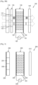
- FIG. 2A shows the birefringence modulator 130 in a first state in which birefringence occurs
- FIG. 2B shows when the birefringence modulator 130 is in a second state in which birefringence does not occur.
- first light L1 incident on the first modulation region 111 of the light modulator 110 is incident on the first transmissive region 121 of the polarization converter 120 in a modulated state.
- second light L2 incident on the second modulation region 112 of the light modulator 110 is incident on the second transmissive region 122 of the polarization converter 120 in a modulated state.
- the light modulator 110 independently modulates phases of the first light L1 and the second light L2.
- Each of the first light L1 and the second light L2 emitted from the light modulator 110 includes a first polarization (for example, s-polarization).
- the first light L1 incident on the first transmissive region 121 of the polarization converter 120 is emitted in a state in which the first polarization (for example, s-polarization) is maintained.
- the second light L2 incident on the second transmissive region 122 of the polarization converter 120 is light undergoing retardation to include second polarization (for example, p-polarization).
- the birefringence modulator 130 may be in the first state (that is, a state in which birefringence occurs) according to a voltage applied thereto.
- a birefringent medium may be of a uniaxial type or a biaxial type.
- the liquid crystal layer 131 of the birefringence modulator 130 of the present invention is not limited to a particular type of birefringence. In the present embodiment, a case in which the liquid crystal layer 131 is uniaxially birefringent will be described as an example.
- an ordinary ray having a polarization direction perpendicular to an optical axis that is an axis of rotational symmetry of the liquid crystal layer 131 and an extraordinary ray having a polarization direction that is not perpendicular to the optical axis of the liquid crystal layer 131 have different velocities.
- the first light L1 is incident on the birefringence modulator 130 so that the first polarization of the first light L1 is perpendicular to a birefringent optical axis of the birefringence modulator 130, and the second light L2 is incident on the birefringence modulator 130 in a state in which the second polarization of the second light L2 is inclinded with respect to the birefringent optical axis of the birefringence modulator 130.
- the first light L1 and the second light L2 have different velocities in the liquid crystal layer 131 of the birefringence modulator 130 and thus have different light paths.
- the first light L1 When the first light L1 is incident perpendicular to the birefringence modulator 130 in a state in which the first light L1 becomes a first polarization (s-polarization), and the second light L2 is incident perpendicular to the birefringence modulator 130 in a state in which the second light L2 becomes a second polarization (p-polarization), the first light L1 undergoes normal refraction and thus travel in the liquid crystal layer 131 in a straight line without being refracted, and then is emitted from the liquid crystal layer 131.
- s-polarization first polarization
- p-polarization second polarization
- the second light L2 is refracted by subnormal refraction in the liquid crystal layer 131 due to birefringence of the birefringence modulator 130, and then is emitted from the liquid crystal layer 131. Therefore, a pitch interval P1 between the first modulation region 111 of the light modulator 110 (and the first transmissive region 121 of the polarization converter 120) and the second modulation region of the light modulator 110 (and the second transmissive region 122 of the polarization converter 120), and a thickness (T1) of the liquid crystal layer 131 of the birefringence modulator 130 are appropriately designed, the second light L2 is emitted from the birefringence modulator 130 in a state in which the second light L2 is refracted to be combined with the first light L1.
- the birefringence modulator 130 when the birefringence modulator 130 is in the first state (birefringent), the first and second light L1 and L2 passing through the birefringence modulator 130 are emitted from the birefringence modulator 130 in a state in which the first and second light L1 and L2 are combined into one light that is incident on the polarizer 140.
- the light passing through the polarizer 140 is provided as a component of a polarization direction of the polarizer 140 of the first light L1 and the second light L2.
- a phase of the light passing through the polarizer 140 is provided as a function of a modulated phase of the first light L1 and a modulated phase of the second light L2.
- a magnitude of the light passing through the polarizer 140 is provided as a sum of a projection component of a first polarization direction (for example, an s direction) of the first light L1 and a projection component of a second polarization direction (for example, a p direction) of the second light L2, and this magnitude is also provided as a function of the modulated phase of the first light L1 and the modulated phase of the second light L2. Therefore, a phase and an intensity of emitted light are independently controlled by phase modulation of the first modulation region 111 and the second modulation region 112 of the light modulator 110.
- the first light L1 and the second light L2 is emitted from the birefringence modulator 130 without any change of a light path in the birefringence modulator 130. Therefore, the first light L1 and the second light L2 are emitted through the polarizer 140 in a state in which the first light L1 and the second light L2 are separated from each other.
- the beam combining/spiltting modulator 100 of the present embodiment selectively controls the birefringence modulator 130 in the first state (birefringent) and the second state (non-birefringent).
- the birefringence modulator 130 when the birefringence modulator 130 is controlled in the first state, the first light L1 and the second light L2 incident on the beam combining/splitting modulator 100 are combined and emitted, and an intensity and a phase of emitted light are independently modulated.
- the birefringence modulator 130 is controlled in the second state, the first light L1 and the second light L2 incident on the beam combining/splitting modulator 100 are individually emitted.
- FIG. 3 schematically shows a beam combining/splitting modulator 200 according to another embodiment of the claimed invention.
- a beam combining/splitting modulator 200 of the present embodiment includes a polarizer 210, a birefringence modulator 220, and a light modulator 230.
- the polarizer 210 is a member configured to transmit light polarized in a predetermined direction (for example, linearly polarized light).
- the birefringence modulator 220 is disposed at a rear side of the polarizer 210. In this case, a side on which light is incident from the outside or a light source is referred to as a front side of the polarizer 210. As will be described later, incident light is emitted again into the front of the polarizer 210 via the birefringence modulator 220 and the light modulator 230.
- the birefringence modulator 220 is switched between the first state in which birefringence occurs and the second state in which birefringence does not occure.
- the birefringence modulator 220 includes a liquid crystal layer 221 in which birefringence occurs according to a voltage applied thereto by a drive control unit 225, and electrode layers 222 and 223 which apply a voltage to both ends of the liquid crystal layer 221.
- the liquid crystal layer 221 of the birefringence modulator 220 functions to branch a light path or combine light paths when the liquid crystal layer 221 is birefringent.
- the light modulator 230 is disposed at a rear side of the birefringence modulator 220.
- the light modulator 230 includes the first modulation region 231 and the second modulation region 232 which indenpendently modulate light.
- the first modulation region 231 and the second modulation region 232 are regions on which the first light L1 and the second light L2, into which the light path is separated when the birefringence modulator 220 is in the first state as will be described later, are incident.
- the first modulation region 231 and the second modulation region 232 reflect light while independently modulating a phase of the light.
- the light modulator 230 is a known reflective phase spatial light modulator. Light incident on or reflected from the light modulator 230 remains in a polarized state as it is.
- the polarizer 210, the birefringence modulator 220, the light modulator 230 may all form a flat panel structure, and the beam combining/splitting modulator 200 may be integrated in one flat panel using a known liquid crystal panel manufacturing process.
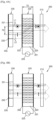
- FIG. 4A shows when the birefringence modulator 220 is in a first state in which birefringence occurs
- FIG. 4B shows when the birefringence modulator 220 is in a second state in which birefringence does not occur.
- light passing through the polarizer 210 is light polarized in a predetermined direction.
- the light may be linearly polarized light having s- polarization or p-polarization components.
- the s-polarization and the p-polarization may be determined based on a birefringent optical axis of the birefringence modulator 220.
- the birefringence modulator 220 may be in the first state (that is, a state in which birefringence occurs) according to a voltage applied thereto.
- first state that is, a state in which birefringence occurs
- first light L1 having a polarization direction (s-polarization) perpendicular to an optical axis that is an axis of rotational symmetry of a liquid crystal layer 221 travels in a straight line without being refracted in the liquid crystal layer 221, but second light L2 having a polarization direction (p-polarization) that is not perpendicular to the optical axis of the liquid crystal layer 221 is refracted in the liquid crystal layer 221.
- the first light L1 and the second light L2 are emitted from the birefringence modulator 220 in a state in which the first light L1 and the second light L2 are separated from each other.
- the first light L1 and the second light L2 emitted from the birefringence modulator 220 are incident on a first modulation region 231 and a second modulation region 232 of the light modulator 230.
- the first light L1 and the second light L2 incident on the first modulation region 231 and the second modulation region 232 of the light modulator 230 independently undergo phase modulation, are reflected, and are incident again on the birefringence modulator 220.
- the first light L1 and the second light L2 that are incident again on a rear side of the birefringence modulator 220 may travel in an opposite direction along the light path before separation, and are emitted from a front side of the birefringence modulator 220 in a state in which the first light L1 and the second light L2 are combined with each other.
- the first and second light L1 and L2 passing through the birefringence modulator 220 are emitted in a state in which the first and second light L1 and L2 are combined with each other and are incident again on the polarizer 210.
- a polarization axis of the polarizer 210 is installed to be inclined with respect to first polarization of the first light L1 and second polarization of the second light L2, the light passing through the polarizer 210 is provided as components of polarization directions of the polarizer 210 of the first light L1 and the second light L2. That is, a phase of the light passing through the polarizer 210 is provided as a function of a modulated phase of the first light L1 and a modulated phase of the second light L2.
- the birefringence modulator 220 when the birefringence modulator 220 is in the second state (that is, a state in which birefringence does not occur), the light incident from the front side of the polarizer 210 is incident on the light modulator 230 without any change of a light path in the birefringence modulator 220.
- the light incident on the first modulation region 231 and the second modulation region 232 of the light modulator 230 is emitted again via the polarizer 210 without any change of the light path in the birefringence modulator 220.
- an intensity and a phase of the light incident from the front side of the polarizer 210 are understood to be independently modulated while the light is emitted again in front of the polarizer 210.
- the beam combining/splitting modulators 100 and 200 of the above-mentioned embodiments since two incident lights may be emitted in a state in which the lights are combined or separated, the beam combining/splitting modulators 100 and 200 operate as an active polarization beam combiner/splitter.
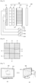
- FIG. 5 schematically shows a display panel 300 according to still another embodiment of the claimed invention
- FIG. 6 shows an example of a pixel array of the display panel 300.
- a display panel 300 of the present embodiment is an application of the beam combining/splitting modulators according to the above-mentioned embodiments.
- the display panel 300 includes a pixel array having a plurality of pixels arranged in a two-dimensional fashion, and each pixel of the pixel array includes a first and/or second modulation region of the beam combining/splitting modulator (100 of FIG. 1 ) of the above-mentioned embodiment.
- the display panel 300 of the present embodiment may further include a color filter 310. When the color filter 310 is further provided, red (R), green (G) and blue (B) subpixels or just some of these may form a pixel.
- the light modulator 110 described above includes first and second modulation regions 111 and 112, first and second transmissive regions 121 and 122 of a polarization converter 120, a birefringence modulator 130, and a polarizer 140.
- the birefringence modulator 130 may be driven according to the red(R), the green (G), and the blue (B) subpixels or integrally. It may also be possible to display a color in a time division scheme performed by sequentially driving red, green, and blue light sources, instead of a spatial division scheme using the color filter 310.
- the display panel 300 of the present embodiment is used as a hologram display panel displaying a computer generated hologram (CGH). Furthermore, the display panel 300 of the present embodiment may also function as a multi-way three dimensional (3D) display panel providing multi-views by appropriately controlling a phase of light. In addition, in the display panel 300 of the present embodiment, the beam combining/splitting modulator 100 may also display a two-dimensional (2D) image by controlling only an intensity of emitted light.
- 2D two-dimensional
- the first and second modulation regions 111 and 112 of the light modulator 110 may individually correspond to pixels (or subpixels).
- a resolution of the 2D image may be twice that of a 3D image.
- the beam combining/splitting modulator 100 described with reference to FIGS. 1, 2A , and 2B is described as an example, it is possible to apply the beam combining/splitting modulator 200 described with reference to FIGS. 3 , 4A, and 4B to a pixel (or a subpixel) of the display panel.
- FIG. 7 schematically shows a display apparatus 400 according to still another embodiment of the present invention.
- the display apparatus 400 includes a display panel 410.
- the display panel 410 is the display panel 300.
- the display apparatus 400 since a beam combining/splitting modulator (100 of FIG. 1 , and 200 of FIG. 3 ) applied to the display panel 410 controls a phase and an intensity of emitted light, the CGH is displayed. Therefore, the display apparatus 400 also functions as a holographic image display apparatus. Furthermore, as described above, since the display panel 410 may also function as a multi-way 3D display panel providing a multi-view by appropriately controlling the phase of light, the display panel 410 may also function as a 3D display apparatus providing a multi-view.
- the beam combining/splitting modulators 100 and 200 may selectively control only an intensity of emitted light L1 and L2, the display apparatus 400, in a not claimed example, may also function as a 2D/3D switchable stereoscopic image display apparatus.
- the display panel 410 using the beam combining/ splitting modulator 100 or 200 may also be a flat panel.
- the display apparatus 400 may also be a flat panel display apparatus.
- a beam combining/splitting modulator and a spatial light modulation method control a phase and an intensity of incident light.
- a beam combining/splitting modulator and a spatial light modulation method emit two incident light in a state in which the two incident lights are combined or splitted.
- a beam combining/splitting modulator according to the embodiments of the claimed invention is also used as a complex spatial light modulator (a display panel) configured to display a holographic image.
- a display apparatus is also a holographic display apparatus configured to display a holographic image.
Landscapes
- Physics & Mathematics (AREA)
- Nonlinear Science (AREA)
- General Physics & Mathematics (AREA)
- Optics & Photonics (AREA)
- Mathematical Physics (AREA)
- Chemical & Material Sciences (AREA)
- Crystallography & Structural Chemistry (AREA)
- Liquid Crystal (AREA)
- Optical Modulation, Optical Deflection, Nonlinear Optics, Optical Demodulation, Optical Logic Elements (AREA)
Description
- The present disclosure relates to a beam combining/splitting modulator, a display apparatus using the same, and a spatial light modulation method.
- In recent years, many three-dimensional (3D) movies are appearing, and thus many techniques related to 3D image display apparatuses are being studied. Since the 3D image display apparatuses display 3D images based on binocular parallax, 3D image display apparatuses which are being currently commercialized use binocular parallax of two eyes of a viewer. As a left-eye image and a right-eye image having different viewpoints are provided to the left and right eyes of a viewer, the viewer may perceive a stereoscopic effect. Such 3D image display apparatuses may include
glasses type 3D image display apparatuses for which special glasses are necessary and non-glassestype 3D image display apparatuses for which glasses are not necessary. - However, when the viewer watches a 3D image displayed in a binocular parallax fashion, the viewer's eyes feel very tired, and 3D image display apparatuses configured to provide only two viewpoints, i.e., a left-eye image and a right-eye image, do not reflect a viewpoint change according to the movement of the viewer. As such, there is a limitation in providing a natural stereoscopic effect to the viewer.
- In order to display more natural stereoscopic images, holographic display apparatuses are being studied. Light may be considered to be waves having amplitude information and phase information. A holography technique controls a phase and an amplitude of light to display an image. Accordingly, in the holographic display apparatuses, a device capable of controlling an amplitude (intensity) and a phase of light is necessary.
- German patent application
DE 10 2012 101 183 A1 teaches a holographic display using an optical beam combiner for combining two pixels of a spatial light modulator to generate complex pixels. US patent applicationUS 2012/0092735 A1 teaches a three-dimensional light modulator, of which the pixels are combined to form modulation elements wherein each modulation element can be coded with a preset discrete value such that three-dimensionally arranged object points can be holographically reconstructed. International patent applicationWO 2010/149583 A1 teaches a lighting device having a planer optical fiber and at least one light source device for illuminating a controllable spatial light modulator wherein the optical fiber comprises a light-conducting core and a cover coating, and the light modulator comprises a pixel matrix, the light source device is disposed on the side of the optical fiber, and the light emitted by at least one light source of the light source device propagates laminarly in the optical fiber. - In a display apparatus adapted for switching between a holographic and two-dimensional display mode, device capable of switching between the holographic display mode and the two-dimensional display mode is necessary.
- Provided is a beam combining/splitting modulator capable of selectively combining or splitting light according to one of claims 1-3.
- Provided is a display apparatus, according to claim 4, configured to display an image by using the beam combining/splitting modulator.
- Provided is a spatial light modulation method for modulating a phase and an intensity of light by using the beam combining/splitting modulator according to one of claims 5 and 6.
- Additional aspects will be set forth in part in the description which follows and, in part, will be apparent from the description.
- These and/or other aspects will become apparent and more readily appreciated from the following description of the embodiments, taken in conjunction with the accompanying drawings in which:
-
FIG. 1 schematically shows a beam combining/splitting modulator according to an embodiment of the present invention; -
FIGS. 2A and2B are views for describing an operation of the beam combining/splitting modulator ofFIG. 1 ; -
FIG. 3 schematically shows a beam combining/splitting modulator according to another embodiment of the present invention; -
FIGS. 4A and 4B are views for describing an operation of the beam combining/ splitting modulator ofFIG. 3 ; -
FIG. 5 schematically shows a display panel according to still another embodiment of the present invention; -
FIG. 6 shows an example of a pixel array of the display panel ofFIG. 5 ; and -
FIG. 7 schematically shows a display apparatus according to still another embodiment of the present invention. - According to the claimed invention, a beam combining/splitting modulator is provided according to claim 1.
- Preferred embodiments are subject of the dependent claims.
- According to another aspect of the claimed invention, a beam combining/splitting modulator is provided according to claim 3.
- Preferred embodiments are subject of the dependent claims.
- According to still another aspect of the claimed invention, a display apparatus is provided according to claim 4.
- According to still another aspect of the claimed invention, a spatial light modulation method is provided according to claim 5.
- According to still another aspect of the claimed invention, a spatial light modulation method is provided according to claim 6.
- Reference will now be made in detail to embodiments, examples of which are illustrated in the accompanying drawings, wherein like reference numerals refer to like elements throughout. Expressions such as "at least one of," when preceding a list of elements, modify the entire list of elements and do not modify the individual elements of the list.
- Hereinafter, exemplary embodiments of the claimed invention will be described in detail with reference to the accompanying drawings. In the following drawings, the same reference numerals indicate the same components, and in the drawings, sizes of elements may be exaggerated for clarity and convenience of the description.
-
FIG. 1 schematically shows a beam combining/splittingmodulator 100 according to an embodiment of the claimed invention. - A beam combining/
splitting modulator 100 of the present embodiment includes alight modulator 110, apolarization converter 120, abirefringence modulator 130, and apolarizer 140. - The
light modulator 110 includes a first modulation region 111 and asecond modulation region 112 which independently modulate light. The first modulation region 111 and thesecond modulation region 112 independently modulate a phase of light. Light passing through thelight modulator 110 has a predetermined polarized state. For example, light emitted from thelight modulator 110 may be linearly polarized light. A polarization direction of light emitted from thelight modulator 110 may be considered as, for example, an s-polarized wave in relation to thebirefringence modulator 130 which will be described later. Thelight modulator 110 may be a known transmissive phase spatial light modulator. As an example, thelight modulator 110 may be a light modulator for a parallel-aligned nematic-liquid-crystal (PAL) panel. The PAL panel may be configured so that rubbing directions (that is, orientation directions of liquid crystal) of upper and lower plates are parallel to each other (at 180°). When liquid crystal is oriented by performing rubbing in directions in which the upper and lower plates are anti-parallel a positive type liquid crystal may be used. As such, when a voltage is applied, the liquid crystal may stand at a tilt angle perpendicular to the upper and lower plates without twisting. Therefore, phase modulation and control of a birefringence state may be possible without changing amplitude. As another example, thelight modulator 110 may be a light modulator for a vertically aligned (VA) LC (liquid-crystal) panel. Even though the VA LC panel has an initial orientation of a liquid crystal perpendicular to the upper and lower plates, a negative type liquid crystal may be used. As such, when a voltage is applied, the liquid crystal may be reoriented in a direction perpendicular to an electric field. Therefore, even in this case, phase modulation and control of a birefringence state may be possible without twisting the liquid crystal. - The
polarization converter 120 is disposed at a side of an emitting surface of thelight modulator 110. Thepolarization converter 120 includes a firsttransmissive region 121 and a secondtransmissive region 122. The firsttransmissive region 121 is a region corresponding to the first modulation region 111 of thelight modulator 110, and polarizes and converts light (hereinafter, referred to as first light) L1 incident from the first modulation region 111 of thelight modulator 110 so that the light L1 have a first polarization (for example, s-polarization). The secondtransmissive region 122 is a region corresponding to thesecond modulation region 112 of thelight modulator 110, and polarizes and converts light (hereinafter, referred to as second light) L2 incident from thesecond modulation region 112 of thelight modulator 110 so that the light L2 have a second polarization (for example, p-polarization). The meaning of polarizing and converting light may be broadly considered to include maintaining polarization of incident light. As an example, the firsttransmissive region 121 of thepolarization converter 120 may have no retardation of phase, and the secondtransmissive region 122 of thepolarization converter 120 may be a region of a half-wave plate for retarding a half-wave phase. - The
birefringence modulator 130 is disposed at the side of the emitting surface of thepolarization converter 120. Thebirefringence modulator 130 is an active modulator which switches between a first state in which birefringence occurs and a second state in which birefringence does not occur. Thebirefringence modulator 130 includes aliquid crystal layer 131 in which birefringence occurs according to a voltage applied thereto from adrive control unit 135, andelectrode layers liquid crystal layer 131. Since theliquid crystal layer 131 of thebirefringence modulator 130 functions to branch light or couple lights when theliquid crystal layer 131 is in birefringent state as will be described later, a thickness (T1 ofFIG. 2A ) of theliquid crystal layer 131 is designed to sufficiently branch or couple a light path changed by birefringence of theliquid crystal layer 131 as will be described later. - The
polarizer 140 is disposed at the side of the emitting surface of thebirefringence modulator 130. A polarization axis of thepolarizer 140 is inclined with respect to the first polarization and the second polarization. In other words, thepolarizer 140 is installed so that light passing through thepolarizer 140 include both a projection component with respect to the polarization axis of the first polarization and a projection component with respect to the polarization axis of the second polarization. As an example when the first polarization is s-polarization, and the second polarization is p-polarization, the polarization axis of thepolarizer 140 is installed so as to be inclined with respect to both an s-polarization direction and a p-polarization direction. - On the other hand, the
light modulator 110, thepolarization converter 120, thebirefringence modulator 130, and thepolarizer 140 may all form a flat panel structure. The beam combining/splitting modulator 100 may be integrated into one flat panel using a known liquid crystal panel manufacturing process. - Next, a spatial light modulation method for use wih the beam combining/
splitting modulator 100 will be described with reference toFIGS. 2A and2B .FIG. 2A shows thebirefringence modulator 130 in a first state in which birefringence occurs, andFIG. 2B shows when thebirefringence modulator 130 is in a second state in which birefringence does not occur. - First, referring to
FIG. 2A , first light L1 incident on the first modulation region 111 of thelight modulator 110 is incident on the firsttransmissive region 121 of thepolarization converter 120 in a modulated state. Similarly, second light L2 incident on thesecond modulation region 112 of thelight modulator 110 is incident on the secondtransmissive region 122 of thepolarization converter 120 in a modulated state. Thelight modulator 110 independently modulates phases of the first light L1 and the second light L2. Each of the first light L1 and the second light L2 emitted from thelight modulator 110 includes a first polarization (for example, s-polarization). - The first light L1 incident on the first
transmissive region 121 of thepolarization converter 120 is emitted in a state in which the first polarization (for example, s-polarization) is maintained. The second light L2 incident on the secondtransmissive region 122 of thepolarization converter 120 is light undergoing retardation to include second polarization (for example, p-polarization). - The
birefringence modulator 130 may be in the first state (that is, a state in which birefringence occurs) according to a voltage applied thereto. - In general, light passing through a birefringent body may have different velocities according to a polarization direction thereof. A birefringent medium may be of a uniaxial type or a biaxial type. The
liquid crystal layer 131 of thebirefringence modulator 130 of the present invention is not limited to a particular type of birefringence. In the present embodiment, a case in which theliquid crystal layer 131 is uniaxially birefringent will be described as an example. - When the
birefringence modulator 130 is in a first state (birefringent), an ordinary ray having a polarization direction perpendicular to an optical axis that is an axis of rotational symmetry of theliquid crystal layer 131 and an extraordinary ray having a polarization direction that is not perpendicular to the optical axis of theliquid crystal layer 131 have different velocities. Therefore, when thebirefringence modulator 130 is in the first state (birefringent), the first light L1 is incident on thebirefringence modulator 130 so that the first polarization of the first light L1 is perpendicular to a birefringent optical axis of thebirefringence modulator 130, and the second light L2 is incident on thebirefringence modulator 130 in a state in which the second polarization of the second light L2 is inclinded with respect to the birefringent optical axis of thebirefringence modulator 130. The first light L1 and the second light L2 have different velocities in theliquid crystal layer 131 of thebirefringence modulator 130 and thus have different light paths. When the first light L1 is incident perpendicular to thebirefringence modulator 130 in a state in which the first light L1 becomes a first polarization (s-polarization), and the second light L2 is incident perpendicular to thebirefringence modulator 130 in a state in which the second light L2 becomes a second polarization (p-polarization), the first light L1 undergoes normal refraction and thus travel in theliquid crystal layer 131 in a straight line without being refracted, and then is emitted from theliquid crystal layer 131. - However, the second light L2 is refracted by subnormal refraction in the
liquid crystal layer 131 due to birefringence of thebirefringence modulator 130, and then is emitted from theliquid crystal layer 131. Therefore, a pitch interval P1 between the first modulation region 111 of the light modulator 110 (and the firsttransmissive region 121 of the polarization converter 120) and the second modulation region of the light modulator 110 (and the secondtransmissive region 122 of the polarization converter 120), and a thickness (T1) of theliquid crystal layer 131 of thebirefringence modulator 130 are appropriately designed, the second light L2 is emitted from thebirefringence modulator 130 in a state in which the second light L2 is refracted to be combined with the first light L1. - Accordingly, as shown in the drawings, when the
birefringence modulator 130 is in the first state (birefringent), the first and second light L1 and L2 passing through thebirefringence modulator 130 are emitted from thebirefringence modulator 130 in a state in which the first and second light L1 and L2 are combined into one light that is incident on thepolarizer 140. - Since the polarization axis of the
polarizer 140 is inclined with respect to the first polarization and the second polarization, the light passing through thepolarizer 140 is provided as a component of a polarization direction of thepolarizer 140 of the first light L1 and the second light L2. In order words, a phase of the light passing through thepolarizer 140 is provided as a function of a modulated phase of the first light L1 and a modulated phase of the second light L2. In addition, a magnitude of the light passing through thepolarizer 140 is provided as a sum of a projection component of a first polarization direction (for example, an s direction) of the first light L1 and a projection component of a second polarization direction (for example, a p direction) of the second light L2, and this magnitude is also provided as a function of the modulated phase of the first light L1 and the modulated phase of the second light L2. Therefore, a phase and an intensity of emitted light are independently controlled by phase modulation of the first modulation region 111 and thesecond modulation region 112 of thelight modulator 110. - Next, referring to
FIG. 2B , when thebirefringence modulator 130 is in the second state (that is, the state in which birefringence does not occur), the first light L1 and the second light L2 is emitted from thebirefringence modulator 130 without any change of a light path in thebirefringence modulator 130. Therefore, the first light L1 and the second light L2 are emitted through thepolarizer 140 in a state in which the first light L1 and the second light L2 are separated from each other. - As described above, the beam combining/
spiltting modulator 100 of the present embodiment selectively controls thebirefringence modulator 130 in the first state (birefringent) and the second state (non-birefringent). In this case, when thebirefringence modulator 130 is controlled in the first state, the first light L1 and the second light L2 incident on the beam combining/splitting modulator 100 are combined and emitted, and an intensity and a phase of emitted light are independently modulated. When thebirefringence modulator 130 is controlled in the second state, the first light L1 and the second light L2 incident on the beam combining/splitting modulator 100 are individually emitted. -
FIG. 3 schematically shows a beam combining/splitting modulator 200 according to another embodiment of the claimed invention. - A beam combining/
splitting modulator 200 of the present embodiment includes apolarizer 210, abirefringence modulator 220, and alight modulator 230. Thepolarizer 210 is a member configured to transmit light polarized in a predetermined direction (for example, linearly polarized light). Thebirefringence modulator 220 is disposed at a rear side of thepolarizer 210. In this case, a side on which light is incident from the outside or a light source is referred to as a front side of thepolarizer 210. As will be described later, incident light is emitted again into the front of thepolarizer 210 via thebirefringence modulator 220 and thelight modulator 230. - The
birefringence modulator 220 is switched between the first state in which birefringence occurs and the second state in which birefringence does not occure. Thebirefringence modulator 220 includes aliquid crystal layer 221 in which birefringence occurs according to a voltage applied thereto by adrive control unit 225, andelectrode layers liquid crystal layer 221. As will be described later, theliquid crystal layer 221 of thebirefringence modulator 220 functions to branch a light path or combine light paths when theliquid crystal layer 221 is birefringent. A thickness (T2 ofFIG. 4A ) of theliquid crystal layer 221 of thebirefringence modulator 220 and a pitch interval (P2 ofFIG. 4A ) of afirst modulation region 231 and asecond modulation region 232 of thelight modulator 230 are designed to sufficiently branch or couple a light path changed by birefringence of theliquid crystal layer 221 as will be described later. - The
light modulator 230 is disposed at a rear side of thebirefringence modulator 220. Thelight modulator 230 includes thefirst modulation region 231 and thesecond modulation region 232 which indenpendently modulate light. Thefirst modulation region 231 and thesecond modulation region 232 are regions on which the first light L1 and the second light L2, into which the light path is separated when thebirefringence modulator 220 is in the first state as will be described later, are incident. Thefirst modulation region 231 and thesecond modulation region 232 reflect light while independently modulating a phase of the light. Thelight modulator 230 is a known reflective phase spatial light modulator. Light incident on or reflected from thelight modulator 230 remains in a polarized state as it is. - On the other hand, the
polarizer 210, thebirefringence modulator 220, thelight modulator 230 may all form a flat panel structure, and the beam combining/splitting modulator 200 may be integrated in one flat panel using a known liquid crystal panel manufacturing process. - Next, an operation of the beam combining/
splitting modulator 200 of the present embodiment will be described with reference toFIGS. 4A and 4B. FIG. 4A shows when thebirefringence modulator 220 is in a first state in which birefringence occurs, andFIG. 4B shows when thebirefringence modulator 220 is in a second state in which birefringence does not occur. - First, referring to
FIG. 4A , light passing through thepolarizer 210 is light polarized in a predetermined direction. As an example, the light may be linearly polarized light having s- polarization or p-polarization components. In this case, the s-polarization and the p-polarization may be determined based on a birefringent optical axis of thebirefringence modulator 220. - The
birefringence modulator 220 may be in the first state (that is, a state in which birefringence occurs) according to a voltage applied thereto. When thebirefringence modulator 220 is in the first state (birefringent), first light L1 having a polarization direction (s-polarization) perpendicular to an optical axis that is an axis of rotational symmetry of aliquid crystal layer 221 travels in a straight line without being refracted in theliquid crystal layer 221, but second light L2 having a polarization direction (p-polarization) that is not perpendicular to the optical axis of theliquid crystal layer 221 is refracted in theliquid crystal layer 221. As a result, the first light L1 and the second light L2 are emitted from thebirefringence modulator 220 in a state in which the first light L1 and the second light L2 are separated from each other. The first light L1 and the second light L2 emitted from thebirefringence modulator 220 are incident on afirst modulation region 231 and asecond modulation region 232 of thelight modulator 230. The first light L1 and the second light L2 incident on thefirst modulation region 231 and thesecond modulation region 232 of thelight modulator 230 independently undergo phase modulation, are reflected, and are incident again on thebirefringence modulator 220. The first light L1 and the second light L2 that are incident again on a rear side of thebirefringence modulator 220 may travel in an opposite direction along the light path before separation, and are emitted from a front side of thebirefringence modulator 220 in a state in which the first light L1 and the second light L2 are combined with each other. The first and second light L1 and L2 passing through thebirefringence modulator 220 are emitted in a state in which the first and second light L1 and L2 are combined with each other and are incident again on thepolarizer 210. Since a polarization axis of thepolarizer 210 is installed to be inclined with respect to first polarization of the first light L1 and second polarization of the second light L2, the light passing through thepolarizer 210 is provided as components of polarization directions of thepolarizer 210 of the first light L1 and the second light L2. That is, a phase of the light passing through thepolarizer 210 is provided as a function of a modulated phase of the first light L1 and a modulated phase of the second light L2. - Next, referring to
FIG 4B , when thebirefringence modulator 220 is in the second state (that is, a state in which birefringence does not occur), the light incident from the front side of thepolarizer 210 is incident on thelight modulator 230 without any change of a light path in thebirefringence modulator 220. The light incident on thefirst modulation region 231 and thesecond modulation region 232 of thelight modulator 230 is emitted again via thepolarizer 210 without any change of the light path in thebirefringence modulator 220. - As described above, according to the beam combining/
splitting modulator 200 of the present embodiment, an intensity and a phase of the light incident from the front side of thepolarizer 210 are understood to be independently modulated while the light is emitted again in front of thepolarizer 210. - According to the beam combining/
splitting modulators splitting modulators -
FIG. 5 schematically shows adisplay panel 300 according to still another embodiment of the claimed invention, andFIG. 6 shows an example of a pixel array of thedisplay panel 300. - Referring to
FIGS. 5 and 6 , adisplay panel 300 of the present embodiment is an application of the beam combining/splitting modulators according to the above-mentioned embodiments. For example, thedisplay panel 300 includes a pixel array having a plurality of pixels arranged in a two-dimensional fashion, and each pixel of the pixel array includes a first and/or second modulation region of the beam combining/splitting modulator (100 ofFIG. 1 ) of the above-mentioned embodiment. In addition, thedisplay panel 300 of the present embodiment may further include acolor filter 310. When thecolor filter 310 is further provided, red (R), green (G) and blue (B) subpixels or just some of these may form a pixel. According to the red (R), the green (G), and the blue (B) subpixels, thelight modulator 110 described above includes first andsecond modulation regions 111 and 112, first and secondtransmissive regions polarization converter 120, abirefringence modulator 130, and apolarizer 140. Thebirefringence modulator 130 may be driven according to the red(R), the green (G), and the blue (B) subpixels or integrally. It may also be possible to display a color in a time division scheme performed by sequentially driving red, green, and blue light sources, instead of a spatial division scheme using thecolor filter 310. - As described above, since the beam combining/
splitting modulator 100 may combine two incident lights to independently control the phase and intensity of the light, the phase and the intensity of the emitted light may be controlled according to each pixel (or subpixel). Therefore, thedisplay panel 300 of the present embodiment is used as a hologram display panel displaying a computer generated hologram (CGH). Furthermore, thedisplay panel 300 of the present embodiment may also function as a multi-way three dimensional (3D) display panel providing multi-views by appropriately controlling a phase of light. In addition, in thedisplay panel 300 of the present embodiment, the beam combining/splitting modulator 100 may also display a two-dimensional (2D) image by controlling only an intensity of emitted light. When a 2D image is displayed (that is, when only an intensity of light is modulated), the first andsecond modulation regions 111 and 112 of thelight modulator 110 may individually correspond to pixels (or subpixels). Thus, a resolution of the 2D image may be twice that of a 3D image. - In addition, in the
display panel 300 of the above-mentioned embodiment, even though the beam combining/splitting modulator 100 described with reference toFIGS. 1, 2A , and2B is described as an example, it is possible to apply the beam combining/splitting modulator 200 described with reference toFIGS. 3 ,4A, and 4B to a pixel (or a subpixel) of the display panel. -
FIG. 7 schematically shows adisplay apparatus 400 according to still another embodiment of the present invention. Thedisplay apparatus 400 includes adisplay panel 410. Thedisplay panel 410 is thedisplay panel 300. - As described above, since a beam combining/splitting modulator (100 of
FIG. 1 , and 200 ofFIG. 3 ) applied to thedisplay panel 410 controls a phase and an intensity of emitted light, the CGH is displayed. Therefore, thedisplay apparatus 400 also functions as a holographic image display apparatus. Furthermore, as described above, since thedisplay panel 410 may also function as a multi-way 3D display panel providing a multi-view by appropriately controlling the phase of light, thedisplay panel 410 may also function as a 3D display apparatus providing a multi-view. In addition, in a not claimed example, the beam combining/splitting modulators display apparatus 400, in a not claimed example, may also function as a 2D/3D switchable stereoscopic image display apparatus. - In addition, since the beam combining/
splitting modulator display panel 410 using the beam combining/splitting modulator display apparatus 400 may also be a flat panel display apparatus. - As described above, according to the one or more of the above embodiments of the claimed invention, a beam combining/splitting modulator and a spatial light modulation method according to the embodiments of the claimed invention control a phase and an intensity of incident light.
- A beam combining/splitting modulator and a spatial light modulation method according to embodiments of the claimed invention emit two incident light in a state in which the two incident lights are combined or splitted.
- A beam combining/splitting modulator according to the embodiments of the claimed invention is also used as a complex spatial light modulator (a display panel) configured to display a holographic image.
- A display apparatus according to the embodiments of the claimed invention is also a holographic display apparatus configured to display a holographic image.
Claims (6)
- A beam combining/splitting modulator (100) comprising:a transmissive phase spatial light modulator (110) including first and second modulation regions (111, 112) for independently modulating a phase of incident light and configured to pass incident light as polarized light with a predetermined polarized state;a polarization converter (120) disposed at a side of an emitting surface of the transmissive phase spatial light modulator (110), and including a first transmissive region (121) for polarizing and converting light incident from the first modulation region (111) to have a first polarization and a second transmissive region (122) for polarizing and converting light incident from the second modulation region (112) to have a second polarization;a birefringence modulator (130) disposed at the side of an emitting surface of the polarization converter (120) and including a liquid crystal layer (131) in which birefringence occurs according to a voltage applied thereto; anda polarizer (140) disposed at the side of an emitting surface of the birefringence modulator (130);wherein a polarization axis of the polarizer (140) is inclined with respect to the first and second polarization;characterized in thatthe birefringence modulator (130) is configured to switch between a first state in which birefringence occurs and a second state in which birefringence does not occur;wherein, when the birefringence modulator is in the first state, a light path of at least one light of the light incident from the first modulation region (111) and the light incident from the second modulation region (112) is changed in the birefringence modulator (130), the incident lights are combined, and the combined light is emitted from the birefringence modulator (130), and when the birefringence modulator is in the second state, the light incident from the first modulation region (111) and the light incident from the second modulation region (112) are emitted from the birefringence modulator (130) without any change of light paths thereof.
- The beam combining/splitting modulator (100) of claim 1, wherein a first transmissive region (121) of the polarization converter (120) has no retardation, and a second transmissive region (122) of the polarization converter (120) is a region of a half-wave plate for retarding a half-wave phase.
- A beam combining/splitting modulator (200) comprising:a polarizer (210) on which light is incident;a birefringence modulator (220) disposed at a rear side of the polarizer (210) and including a liquid crystal layer (221) in which birefringence occurs according to a voltage applied thereto; anda reflective phase spatial light modulator (230) disposed at a rear side of the birefringence modulator (220) and including first and second modulation regions (231, 232) for independently modulating a phase of light incident from the birefringence modulator (220) and reflecting the modulated light to the birefringence modulator (220);characterized in thatthe birefringence modulator (220) is configured to switch between a first state in which birefringence occurs and a second state in which birefringence does not occur;wherein, when the birefringence modulator (220) is in the first state, light polarized in the polarizer (210) is split into first light of a first polarization and second light of a second polarization in the birefringence modulator (220), a polarization axis of the polarizer (210) being inclined with respect to the first and second polarization, each of the first and second lights are incident on the first and second modulation regions (231, 232) of the reflective phase spatial light modulator (230), a phase of the first light and a phase of the second light are independently modulated in the first and second modulation regions (231, 232) of the reflective phase spatial light modulator (230), the first and second lights are incident again on and are recombined in the birefringence modulator (220), and the recombined light is emitted through the polarizer (210), andwhen the birefringence modulator (220) is in the second state, light polarized in the polarizer is incident on the reflective phase spatial light modulator (230) without being split in the birefringence modulator (220), is modulated in the reflective phase spatial light modulator (230), and is emitted through the polarizer (210) via the birefringence modulator (220).
- A display apparatus (400) adapted for switching between a holographic and a two-dimensional display mode, the display apparatus (400) comprising a display panel (300, 410) including a pixel array having a plurality of pixels that are arranged in a two-dimensional fashion and the beam combining/splitting modulator (100, 200) according to one of the preceding claims, wherein each of the plurality of pixels of the pixel array includes a first and/or second modulation region (111,112, 231, 232) of the beam combining/splitting modulator (100, 200).
- A spatial light modulation method comprising:independently modulating a phase of light incident on first and second modulation regions (111, 112) of a transmissive phase spatial light modulator (110);passing incident light as polarized light with a predetermined polarization state by the transmissive phase spatial light modulator (110);polarizing and converting, by a polarization converter (120), light passing through the first modulation region (111) to have a first polarization and light passing through the second modulation region (112) to have a second polarization;causing the polarized and converted light to be incident on a birefringence modulator (130) including a liquid crystal layer (131) in which birefringence occurs according to a voltage applied thereto; andpassing light that has passed through the birefringence modulator (130) through a polarizer (140);wherein a polarization axis of the polarizer (140) is inclined with respect to the first and second polarization;characterized bycontrolling the birefringence modulator (130) so that the birefringence modulator (130) is in any one of a first state in which birefringence occurs and a second state in which birefringence does not occur;wherein, when the birefringence modulator (130) is in the first state, a light path of at least one of light incident from the first modulation region (111) and light incident from the second modulation region (112) is changed in the birefringence modulator (130), the incident lights are combined, and the combined light is emitted from the birefringence modulator (130), andwhen the birefringence modulator (130) is in the second state, the light incident from the first modulation region (111) and the light incident from the second modulation region (112) are emitted from the birefringence modulator without any change of light paths thereof.
- A spatial light modulation method comprising:passing incident light through a polarizer (210);causing the light passing through the polarizer (210) to be incident on a birefringence modulator (220) including a liquid crystal layer (221) in which birefringence occurs according to a voltage applied thereto;causing light passing through the birefringence modulator (220) to be incident on first and second modulation regions (231, 232) of a reflective phase spatial light modulator (230);independently modulating and reflecting light incident on the first and second modulation regions (231, 232) of the reflective phase spatial light modulator (230);causing the reflected light to be again incident on the birefringence modulator (220); andpassing light that has passed through the birefringence modulator (220) again through the polarizer (210);characterized bycontrolling the birefringence modulator (220) so that the birefringence modulator (220) is in any one of a first state in which birefringence occurs and a second state in which birefringence does not occur;wherein, when the birefringence modulator (220) is in the first state, light polarized in the polarizer (210) is separated into first light of a first polarization and second light of a second polarization in the birefringence modulator (220), the separated lights are incident on the first and second modulation regions (231, 232) of the reflective phase spatial light modulator (230), phases of the incident lights are independently modulated in the first and second modulation regions (231, 232) of the reflective phase spatial light modulator (230), the modulated lights are incident again on and recombined in the birefringence modulator (220), and the recombined light is emitted through the polarizer (210), wherein a polarization axis of the polarizer (210) is inclined with respect to the first and second polarization, andwhen the birefringence modulator (220) is in the second state, light polarized in the polarizer (210) is incident on the reflective phase spatial light modulator (230) without being separated in the birefringence modulator (220), is modulated in the reflective phase spatial light modulator (230), and is emitted through the polarizer (210) via the birefringence modulator (220).
Applications Claiming Priority (2)
| Application Number | Priority Date | Filing Date | Title |
|---|---|---|---|
| KR1020130154102A KR102188077B1 (en) | 2013-12-11 | 2013-12-11 | Beam combine/split modulator, display apparatus using the same, and method for modulating spatial light |
| PCT/KR2014/012108 WO2015088236A1 (en) | 2013-12-11 | 2014-12-10 | Beam modulator and display apparatus using the same |
Publications (3)
| Publication Number | Publication Date |
|---|---|
| EP3080658A1 EP3080658A1 (en) | 2016-10-19 |
| EP3080658A4 EP3080658A4 (en) | 2017-08-09 |
| EP3080658B1 true EP3080658B1 (en) | 2025-02-19 |
Family
ID=53371467
Family Applications (1)
| Application Number | Title | Priority Date | Filing Date |
|---|---|---|---|
| EP14869044.9A Active EP3080658B1 (en) | 2013-12-11 | 2014-12-10 | Beam modulator and display apparatus using the same |
Country Status (4)
| Country | Link |
|---|---|
| US (1) | US10274755B2 (en) |
| EP (1) | EP3080658B1 (en) |
| KR (1) | KR102188077B1 (en) |
| WO (1) | WO2015088236A1 (en) |
Families Citing this family (7)
| Publication number | Priority date | Publication date | Assignee | Title |
|---|---|---|---|---|
| CN106681054A (en) * | 2017-02-06 | 2017-05-17 | 京东方科技集团股份有限公司 | Backlight module, spatial light modulator, holographic display device and display method thereof |
| US10248081B2 (en) * | 2017-03-10 | 2019-04-02 | Microsoft Technology Licensing, Llc | Holographic phase and amplitude spatial light modulation |
| EP3850420B1 (en) * | 2018-09-14 | 2024-10-30 | Magic Leap, Inc. | Systems and methods for external light management |
| CN115066644B (en) * | 2020-02-06 | 2023-07-25 | 威尔乌集团 | Microlens Array Polarization Recycling Optics for Illumination Optics |
| DE112023000047B4 (en) | 2023-08-04 | 2025-07-10 | Wuhan China Star Optoelectronics Technology Co., Ltd. | Display module and display device |
| CN117492252A (en) * | 2023-08-04 | 2024-02-02 | 武汉华星光电技术有限公司 | Display module and display device |
| CN121276928B (en) * | 2025-12-11 | 2026-02-27 | 北京航空航天大学 | Holographic code phase modulation method |
Family Cites Families (14)
| Publication number | Priority date | Publication date | Assignee | Title |
|---|---|---|---|---|
| JP2005241870A (en) | 2004-02-25 | 2005-09-08 | Olympus Corp | Space modulation unit and image projector |
| TW200718173A (en) * | 2005-07-14 | 2007-05-01 | Koninkl Philips Electronics Nv | Autostereoscopic display apparatus |
| JP4986582B2 (en) * | 2006-11-15 | 2012-07-25 | シチズンホールディングス株式会社 | Liquid crystal light modulation device, liquid crystal light modulation device, and liquid crystal light modulation device driving method |
| DE102007005821B4 (en) * | 2007-01-31 | 2013-11-14 | Seereal Technologies S.A. | A light modulator and method for ensuring minimum amplitude modulation in phase modulating light modulators |
| KR20100068615A (en) | 2008-12-15 | 2010-06-24 | 전북대학교산학협력단 | Fringe-field switching liquid crystal device using cholesteric blue phase liquid crystal |
| DE102009044910B4 (en) * | 2009-06-23 | 2024-09-05 | Seereal Technologies S.A. | Spatial light modulation device for modulating a wave field with complex information |
| CN102576115B (en) | 2009-06-23 | 2015-02-18 | 视瑞尔技术公司 | Lighting unit for direct view display |
| KR20100137725A (en) | 2009-06-23 | 2010-12-31 | 엘지이노텍 주식회사 | Switching stereoscopic filter and switching stereoscopic image display device using the same |
| KR101993566B1 (en) | 2009-12-01 | 2019-06-26 | 시리얼 테크놀로지즈 에스.에이. | Phase modulator for modulating light interacting with the phase modulator |
| WO2012008408A1 (en) * | 2010-07-12 | 2012-01-19 | シャープ株式会社 | Display device |
| KR101208832B1 (en) | 2011-06-10 | 2012-12-06 | 세종대학교산학협력단 | 3d display system using hologram |
| KR101942972B1 (en) | 2011-10-13 | 2019-01-29 | 삼성전자주식회사 | Spatial light modulator, Apparatus for holography 3-dimensional display and Method for modulating spatial light |
| KR101507202B1 (en) | 2011-11-16 | 2015-04-08 | 엘지디스플레이 주식회사 | Spatial Light Modulating Panel Using Transparent Type Liquid Crystal Display Panel And 3D Display Device Using The Same |
| DE102012101183A1 (en) * | 2012-02-14 | 2013-08-14 | Seereal Technologies S.A. | Birefringent body, beam combining assembly and method of making a birefringent body |
-
2013
- 2013-12-11 KR KR1020130154102A patent/KR102188077B1/en active Active
-
2014
- 2014-12-10 US US15/102,400 patent/US10274755B2/en active Active
- 2014-12-10 WO PCT/KR2014/012108 patent/WO2015088236A1/en not_active Ceased
- 2014-12-10 EP EP14869044.9A patent/EP3080658B1/en active Active
Also Published As
| Publication number | Publication date |
|---|---|
| US10274755B2 (en) | 2019-04-30 |
| KR20150068191A (en) | 2015-06-19 |
| US20160320640A1 (en) | 2016-11-03 |
| KR102188077B1 (en) | 2020-12-07 |
| EP3080658A4 (en) | 2017-08-09 |
| EP3080658A1 (en) | 2016-10-19 |
| WO2015088236A1 (en) | 2015-06-18 |
Similar Documents
| Publication | Publication Date | Title |
|---|---|---|
| US10274755B2 (en) | Beam modulator and display apparatus using the same | |
| CN101833170B (en) | Stereoscopic display device | |
| KR102148418B1 (en) | Complex spatial light modulator and 3D image display having the same | |
| EP1965245A1 (en) | Stereoscopic Display Apparatus | |
| US9720246B2 (en) | Complex spatial light modulator and 3D image display including the same | |
| EP0721132A2 (en) | Autostereoscopic display | |
| US8752965B2 (en) | Stereoscopic display apparatus | |
| US5933127A (en) | Electronic stereoscopic display | |
| US10701348B2 (en) | High brightness stereoscopic image screening device using modulator asymmetry drive, and method for operating same | |
| CN102799024A (en) | Two-dimensional/three-dimensional image switchable liquid crystal display | |
| US9360840B2 (en) | Complex spatial light modulator and 3D image display including the same | |
| CN102890344B (en) | 3D display device and 3D display device | |
| KR20160036745A (en) | Multiview image display system and driving method thereof | |
| EP1182488A2 (en) | Spatial light modulator | |
| KR101939271B1 (en) | Complex spatial light modulator and 3D image display having the same | |
| KR20170060508A (en) | Display device | |
| CN102193206A (en) | Image display apparatus | |
| US20180196293A1 (en) | Image display device | |
| KR101188595B1 (en) | Projection type stereoscopic image system and projection method of stereoscopic image | |
| TW202026709A (en) | Light modulation device | |
| CN102364379B (en) | Naked eye stereoscopic display method based on liquid crystal light valve curtain device | |
| KR101854688B1 (en) | Image Display Device and Stereoscopic Display System Using the Same | |
| GB2314167A (en) | Liquid crystal display and polarized spectacles | |
| CN102281453A (en) | Polarization conversion device, polarization conversion method, and display apparatus | |
| JP2013186242A (en) | Display device and electronic apparatus |
Legal Events
| Date | Code | Title | Description |
|---|---|---|---|
| PUAI | Public reference made under article 153(3) epc to a published international application that has entered the european phase |
Free format text: ORIGINAL CODE: 0009012 |
|
| 17P | Request for examination filed |
Effective date: 20160624 |
|
| AK | Designated contracting states |
Kind code of ref document: A1 Designated state(s): AL AT BE BG CH CY CZ DE DK EE ES FI FR GB GR HR HU IE IS IT LI LT LU LV MC MK MT NL NO PL PT RO RS SE SI SK SM TR |
|
| AX | Request for extension of the european patent |
Extension state: BA ME |
|
| DAX | Request for extension of the european patent (deleted) | ||
| A4 | Supplementary search report drawn up and despatched |
Effective date: 20170706 |
|
| RIC1 | Information provided on ipc code assigned before grant |
Ipc: G02B 27/22 20060101ALI20170630BHEP Ipc: G03H 1/22 20060101AFI20170630BHEP Ipc: G02F 1/1347 20060101ALI20170630BHEP Ipc: G02F 1/29 20060101ALI20170630BHEP |
|
| STAA | Information on the status of an ep patent application or granted ep patent |
Free format text: STATUS: EXAMINATION IS IN PROGRESS |
|
| 17Q | First examination report despatched |
Effective date: 20191015 |
|
| P01 | Opt-out of the competence of the unified patent court (upc) registered |
Effective date: 20230530 |
|
| GRAP | Despatch of communication of intention to grant a patent |
Free format text: ORIGINAL CODE: EPIDOSNIGR1 |
|
| STAA | Information on the status of an ep patent application or granted ep patent |
Free format text: STATUS: GRANT OF PATENT IS INTENDED |
|
| RIC1 | Information provided on ipc code assigned before grant |
Ipc: G03H 1/08 20060101ALN20240912BHEP Ipc: G02B 27/28 20060101ALN20240912BHEP Ipc: G03H 1/02 20060101ALN20240912BHEP Ipc: G02F 1/01 20060101ALI20240912BHEP Ipc: G02F 1/1347 20060101ALI20240912BHEP Ipc: G02F 1/29 20060101ALI20240912BHEP Ipc: G03H 1/22 20060101AFI20240912BHEP |
|
| INTG | Intention to grant announced |
Effective date: 20240923 |
|
| RIN1 | Information on inventor provided before grant (corrected) |
Inventor name: JUNG, JAEEUN Inventor name: LEE, HONGSEOK Inventor name: WON, KANGHEE Inventor name: HAN, SEUNGHOON |
|
| GRAS | Grant fee paid |
Free format text: ORIGINAL CODE: EPIDOSNIGR3 |
|
| GRAA | (expected) grant |
Free format text: ORIGINAL CODE: 0009210 |
|
| STAA | Information on the status of an ep patent application or granted ep patent |
Free format text: STATUS: THE PATENT HAS BEEN GRANTED |
|
| AK | Designated contracting states |
Kind code of ref document: B1 Designated state(s): AL AT BE BG CH CY CZ DE DK EE ES FI FR GB GR HR HU IE IS IT LI LT LU LV MC MK MT NL NO PL PT RO RS SE SI SK SM TR |
|
| REG | Reference to a national code |
Ref country code: GB Ref legal event code: FG4D |
|
| REG | Reference to a national code |
Ref country code: CH Ref legal event code: EP |
|
| REG | Reference to a national code |
Ref country code: IE Ref legal event code: FG4D |
|
| REG | Reference to a national code |
Ref country code: DE Ref legal event code: R096 Ref document number: 602014091582 Country of ref document: DE |
|
| REG | Reference to a national code |
Ref country code: NL Ref legal event code: MP Effective date: 20250219 |
|
| PG25 | Lapsed in a contracting state [announced via postgrant information from national office to epo] |
Ref country code: RS Free format text: LAPSE BECAUSE OF FAILURE TO SUBMIT A TRANSLATION OF THE DESCRIPTION OR TO PAY THE FEE WITHIN THE PRESCRIBED TIME-LIMIT Effective date: 20250519 |
|
| PG25 | Lapsed in a contracting state [announced via postgrant information from national office to epo] |
Ref country code: FI Free format text: LAPSE BECAUSE OF FAILURE TO SUBMIT A TRANSLATION OF THE DESCRIPTION OR TO PAY THE FEE WITHIN THE PRESCRIBED TIME-LIMIT Effective date: 20250219 |
|
| PG25 | Lapsed in a contracting state [announced via postgrant information from national office to epo] |
Ref country code: PL Free format text: LAPSE BECAUSE OF FAILURE TO SUBMIT A TRANSLATION OF THE DESCRIPTION OR TO PAY THE FEE WITHIN THE PRESCRIBED TIME-LIMIT Effective date: 20250219 |
|
| PG25 | Lapsed in a contracting state [announced via postgrant information from national office to epo] |
Ref country code: ES Free format text: LAPSE BECAUSE OF FAILURE TO SUBMIT A TRANSLATION OF THE DESCRIPTION OR TO PAY THE FEE WITHIN THE PRESCRIBED TIME-LIMIT Effective date: 20250219 |
|
| REG | Reference to a national code |
Ref country code: LT Ref legal event code: MG9D |
|
| PG25 | Lapsed in a contracting state [announced via postgrant information from national office to epo] |
Ref country code: IS Free format text: LAPSE BECAUSE OF FAILURE TO SUBMIT A TRANSLATION OF THE DESCRIPTION OR TO PAY THE FEE WITHIN THE PRESCRIBED TIME-LIMIT Effective date: 20250619 Ref country code: NO Free format text: LAPSE BECAUSE OF FAILURE TO SUBMIT A TRANSLATION OF THE DESCRIPTION OR TO PAY THE FEE WITHIN THE PRESCRIBED TIME-LIMIT Effective date: 20250519 |
|
| PG25 | Lapsed in a contracting state [announced via postgrant information from national office to epo] |
Ref country code: NL Free format text: LAPSE BECAUSE OF FAILURE TO SUBMIT A TRANSLATION OF THE DESCRIPTION OR TO PAY THE FEE WITHIN THE PRESCRIBED TIME-LIMIT Effective date: 20250219 |
|
| PG25 | Lapsed in a contracting state [announced via postgrant information from national office to epo] |
Ref country code: HR Free format text: LAPSE BECAUSE OF FAILURE TO SUBMIT A TRANSLATION OF THE DESCRIPTION OR TO PAY THE FEE WITHIN THE PRESCRIBED TIME-LIMIT Effective date: 20250219 |
|
| PG25 | Lapsed in a contracting state [announced via postgrant information from national office to epo] |
Ref country code: LV Free format text: LAPSE BECAUSE OF FAILURE TO SUBMIT A TRANSLATION OF THE DESCRIPTION OR TO PAY THE FEE WITHIN THE PRESCRIBED TIME-LIMIT Effective date: 20250219 Ref country code: PT Free format text: LAPSE BECAUSE OF FAILURE TO SUBMIT A TRANSLATION OF THE DESCRIPTION OR TO PAY THE FEE WITHIN THE PRESCRIBED TIME-LIMIT Effective date: 20250620 |
|
| PG25 | Lapsed in a contracting state [announced via postgrant information from national office to epo] |
Ref country code: GR Free format text: LAPSE BECAUSE OF FAILURE TO SUBMIT A TRANSLATION OF THE DESCRIPTION OR TO PAY THE FEE WITHIN THE PRESCRIBED TIME-LIMIT Effective date: 20250520 Ref country code: BG Free format text: LAPSE BECAUSE OF FAILURE TO SUBMIT A TRANSLATION OF THE DESCRIPTION OR TO PAY THE FEE WITHIN THE PRESCRIBED TIME-LIMIT Effective date: 20250219 |
|
| REG | Reference to a national code |
Ref country code: AT Ref legal event code: MK05 Ref document number: 1768844 Country of ref document: AT Kind code of ref document: T Effective date: 20250219 |
|
| PG25 | Lapsed in a contracting state [announced via postgrant information from national office to epo] |
Ref country code: SE Free format text: LAPSE BECAUSE OF FAILURE TO SUBMIT A TRANSLATION OF THE DESCRIPTION OR TO PAY THE FEE WITHIN THE PRESCRIBED TIME-LIMIT Effective date: 20250219 |
|
| PG25 | Lapsed in a contracting state [announced via postgrant information from national office to epo] |
Ref country code: SM Free format text: LAPSE BECAUSE OF FAILURE TO SUBMIT A TRANSLATION OF THE DESCRIPTION OR TO PAY THE FEE WITHIN THE PRESCRIBED TIME-LIMIT Effective date: 20250219 |
|
| PG25 | Lapsed in a contracting state [announced via postgrant information from national office to epo] |
Ref country code: DK Free format text: LAPSE BECAUSE OF FAILURE TO SUBMIT A TRANSLATION OF THE DESCRIPTION OR TO PAY THE FEE WITHIN THE PRESCRIBED TIME-LIMIT Effective date: 20250219 |
|
| PG25 | Lapsed in a contracting state [announced via postgrant information from national office to epo] |
Ref country code: IT Free format text: LAPSE BECAUSE OF FAILURE TO SUBMIT A TRANSLATION OF THE DESCRIPTION OR TO PAY THE FEE WITHIN THE PRESCRIBED TIME-LIMIT Effective date: 20250219 |
|
| PG25 | Lapsed in a contracting state [announced via postgrant information from national office to epo] |
Ref country code: AT Free format text: LAPSE BECAUSE OF FAILURE TO SUBMIT A TRANSLATION OF THE DESCRIPTION OR TO PAY THE FEE WITHIN THE PRESCRIBED TIME-LIMIT Effective date: 20250219 |
|
| PG25 | Lapsed in a contracting state [announced via postgrant information from national office to epo] |
Ref country code: EE Free format text: LAPSE BECAUSE OF FAILURE TO SUBMIT A TRANSLATION OF THE DESCRIPTION OR TO PAY THE FEE WITHIN THE PRESCRIBED TIME-LIMIT Effective date: 20250219 Ref country code: CZ Free format text: LAPSE BECAUSE OF FAILURE TO SUBMIT A TRANSLATION OF THE DESCRIPTION OR TO PAY THE FEE WITHIN THE PRESCRIBED TIME-LIMIT Effective date: 20250219 |
|
| PG25 | Lapsed in a contracting state [announced via postgrant information from national office to epo] |
Ref country code: RO Free format text: LAPSE BECAUSE OF FAILURE TO SUBMIT A TRANSLATION OF THE DESCRIPTION OR TO PAY THE FEE WITHIN THE PRESCRIBED TIME-LIMIT Effective date: 20250219 |
|
| PG25 | Lapsed in a contracting state [announced via postgrant information from national office to epo] |
Ref country code: SK Free format text: LAPSE BECAUSE OF FAILURE TO SUBMIT A TRANSLATION OF THE DESCRIPTION OR TO PAY THE FEE WITHIN THE PRESCRIBED TIME-LIMIT Effective date: 20250219 |
|
| REG | Reference to a national code |
Ref country code: DE Ref legal event code: R097 Ref document number: 602014091582 Country of ref document: DE |
|
| PLBE | No opposition filed within time limit |
Free format text: ORIGINAL CODE: 0009261 |
|
| STAA | Information on the status of an ep patent application or granted ep patent |
Free format text: STATUS: NO OPPOSITION FILED WITHIN TIME LIMIT |
|
| PGFP | Annual fee paid to national office [announced via postgrant information from national office to epo] |
Ref country code: DE Payment date: 20251111 Year of fee payment: 12 |
|
| PGFP | Annual fee paid to national office [announced via postgrant information from national office to epo] |
Ref country code: GB Payment date: 20251113 Year of fee payment: 12 |
|
| PGFP | Annual fee paid to national office [announced via postgrant information from national office to epo] |
Ref country code: FR Payment date: 20251124 Year of fee payment: 12 |
|
| 26N | No opposition filed |
Effective date: 20251120 |