EP3079355B1 - Dual-mode photosensitive pixel with gain stage - Google Patents
Dual-mode photosensitive pixel with gain stage Download PDFInfo
- Publication number
- EP3079355B1 EP3079355B1 EP16164007.3A EP16164007A EP3079355B1 EP 3079355 B1 EP3079355 B1 EP 3079355B1 EP 16164007 A EP16164007 A EP 16164007A EP 3079355 B1 EP3079355 B1 EP 3079355B1
- Authority
- EP
- European Patent Office
- Prior art keywords
- current
- magnitude
- bias control
- light stimulus
- input light
- Prior art date
- Legal status (The legal status is an assumption and is not a legal conclusion. Google has not performed a legal analysis and makes no representation as to the accuracy of the status listed.)
- Active
Links
Images

Classifications
-
- H—ELECTRICITY
- H10—SEMICONDUCTOR DEVICES; ELECTRIC SOLID-STATE DEVICES NOT OTHERWISE PROVIDED FOR
- H10F—INORGANIC SEMICONDUCTOR DEVICES SENSITIVE TO INFRARED RADIATION, LIGHT, ELECTROMAGNETIC RADIATION OF SHORTER WAVELENGTH OR CORPUSCULAR RADIATION
- H10F77/00—Constructional details of devices covered by this subclass
- H10F77/95—Circuit arrangements
-
- H—ELECTRICITY
- H04—ELECTRIC COMMUNICATION TECHNIQUE
- H04N—PICTORIAL COMMUNICATION, e.g. TELEVISION
- H04N25/00—Circuitry of solid-state image sensors [SSIS]; Control thereof
- H04N25/50—Control of the SSIS exposure
- H04N25/57—Control of the dynamic range
- H04N25/571—Control of the dynamic range involving a non-linear response
- H04N25/573—Control of the dynamic range involving a non-linear response the logarithmic type
-
- H—ELECTRICITY
- H04—ELECTRIC COMMUNICATION TECHNIQUE
- H04N—PICTORIAL COMMUNICATION, e.g. TELEVISION
- H04N25/00—Circuitry of solid-state image sensors [SSIS]; Control thereof
- H04N25/50—Control of the SSIS exposure
- H04N25/57—Control of the dynamic range
- H04N25/571—Control of the dynamic range involving a non-linear response
- H04N25/575—Control of the dynamic range involving a non-linear response with a response composed of multiple slopes
-
- H—ELECTRICITY
- H04—ELECTRIC COMMUNICATION TECHNIQUE
- H04N—PICTORIAL COMMUNICATION, e.g. TELEVISION
- H04N25/00—Circuitry of solid-state image sensors [SSIS]; Control thereof
- H04N25/70—SSIS architectures; Circuits associated therewith
- H04N25/76—Addressed sensors, e.g. MOS or CMOS sensors
- H04N25/77—Pixel circuitry, e.g. memories, A/D converters, pixel amplifiers, shared circuits or shared components
Definitions
- the present disclosure relates generally to systems and methods for photosensitive pixels with gain stage, and more specifically to photosensitive pixels with gain stage with linear and logarithmic output modes.
- the mode threshold control module further comprises a current integrator configured to integrate an output current and produce an output voltage on the output node; a logarithmic current amplifier comprising a field effect transistor comprising a source connected to a reference voltage, V log , a gate connected to the source, and a drain connected to the output node; and an integration reset switch connected in series between a reference voltage, V RESET , and the output node.
- a current integrator configured to integrate an output current and produce an output voltage on the output node
- a logarithmic current amplifier comprising a field effect transistor comprising a source connected to a reference voltage, V log , a gate connected to the source, and a drain connected to the output node
- an integration reset switch connected in series between a reference voltage, V RESET , and the output node.
- a photosensitive pixel with gain stage may include a photodetector module configured to receive an input light stimulus and induce a detection current into a detection node in response to a magnitude of the input light stimulus, a current mirror module having a mirrored current node and configured to induce a mirrored current on the mirrored current node in response to the detection current, and a mode threshold control module with an output node and configured to induce a current on the output node corresponding to a combination of the magnitude of the input light stimulus and an amplifier mode.
- the photodetector module may include a detector configured to detect the magnitude of the input light stimulus, a bias control amplifier connected to the detector, and a bias control transistor connected to the bias control amplifier and configured to induce the detection current into the detection node in response to the magnitude of the input light stimulus.
- the detector may include a reverse biased light sensitive diode having an anode and a cathode.
- the amplifier mode may include at least one of a linear integral correlation to the magnitude of the input light stimulus and a logarithmic correlation to the magnitude of the input light stimulus, and wherein the current mirror module has two n-channel field effect transistors.
- any reference to singular includes plural embodiments, and any reference to more than one component or step may include a singular embodiment or step.
- Surface shading lines may be used throughout the figures to denote different parts but not necessarily to denote the same or different materials.
- an input light stimulus may be in form of electromagnetic radiation.
- the input light stimulus may be a light stimulus.
- the input light stimulus is a collimated light stimulus, such as laser light.
- the input light stimulus is any type of electromagnetic radiation, such as gamma rays, ultraviolet light, infrared light, X rays, or any other electromagnetic radiation.
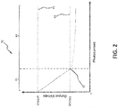
- an example dual-mode photosensitive pixel with gain stage 2 is disclosed ( FIG. 1 ) and various circuit behaviors 40 of the dual-mode photosensitive pixel with gain stage 2 are disclosed ( FIG. 2 ).
- a dual-mode photosensitive pixel with gain stage 2 may be a modified dual-mode current amplifier architecture disclosed herein.
- the dual-mode photosensitive pixel with gain stage 2 may comprise a photodetector module 10, a current mirror module 20, and a mode threshold control module 30.
- a photodetector module 10 may receive an input light stimulus 8 and may establish a detection current into a detection node 15 of the photodetector module 10.
- the current mirror module 20 may monitor the detection node 15 and may further induce a mirrored current on a mirrored current node 25.
- the mirrored current may be amplified or attenuated relative to the detection current on detection node 15
- the mirrored current may be sinked/sourced from a mode threshold control module 30.
- the mode threshold control module 30 may provide an output voltage on an output node 3.
- the output voltage may vary in response to the mirrored current at least one of linearly and logarithmically, depending on the instantaneous mode of operation of the dual-mode photosensitive pixel with gain stage 2.
- output node 3 is reset to an initial voltage, V RESET .
- the mirrored current at mirrored current node 25 will sink charge from output node 3 and the voltage at output node 3 will decrease until a threshold is met.
- the dual-mode photosensitive pixel with gain stage 2 will be operating in a linear (integrating) mode. After the threshold (inflection point 45 on FIG. 2 ) is met, the output voltage at output node 3 will be a substantially instantaneous function of the mirrored current on mirrored current node 25.
- the dual-mode photosensitive pixel with gain stage 2 will be operating in a logarithmic (substantially instantaneous) mode.
- a photodetector module 10 may comprise a detector 11, a bias control amplifier 12, and a bias control transistor 13.
- the photodetector module 10 may receive the input light stimulus 8 and induce a detection current in the detection node 15 in response.
- a detector 11 may comprise an optical detection device.
- the detector 11 may comprise a light sensing diode having an anode and a cathode.
- the light sensing diode may be reverse biased by a voltage, D SUB , and may conduct an illumination response current in response to the presence of an input light stimulus 8.
- a bias control amplifier 12 may comprise an operational amplifier or any other amplifier device.
- the bias control amplifier 12 may be electrically connected in series with the detector 11.
- the bias control amplifier 12 may have a first input 51, a second input 52, and an output 53.
- the detector 11 may be connected to the first input 51.
- a bias control transistor 13 may also be connected in series with the detector 11, such as along a drain-source path of the bias control transistor 13, and the bias control transistor 13 may be connected to the output 53 of the bias control amplifier 12.
- the gate of the bias control transistor 13 may be connected to the output 53 of the bias control amplifier 12, thus the drain-source path of the bias control transistor 13 and the first input 51 of the bias control amplifier 12 may be connected in parallel.
- the bias control amplifier 12 may receive a reference voltage, V REF , such as at the second input 52, and may induce an output 53 in response to a first comparison of the first input 51 and the second input 52.
- the first comparison may comprise the voltage received from the detector 11 being greater than or less than/equal to V REF .
- the first comparison may comprise the voltage received from the detector 11 being greater than/equal to or less than V REF .
- the induced output 53 might may toggle between relatively higher and lower voltages/currents and/or impedances.
- the output 53 of the bias control amplifier 12 may be induced to a lowered voltage.
- the resistivity of the drain-source path of the bias control transistor 13 may change in response. More specifically, the bias control amplifier 12 may monitor the first input 51 (connected to detector 11) and provide a negative feedback path to control the impedance of bias control transistor 13 in response to the detector current at first input 51, such that the first input 51 connected to detector 11 may always be biased as a reference voltage, V REF ,
- a bias control transistor 13 may comprise a field-effect transistor (FET).
- the bias control transistor 13 may comprise a P-channel FET as illustrated in FIG. 1 .
- the bias control transistor 13 may comprise an N-channel FET, or may comprise any transistor as desired.
- the bias control transistor 13 may comprise a P-channel FET having a gate, drain, and source.
- the gate may be connected to the output of the bias control amplifier 12 so that the bias control amplifier 12 provides feedback inducing the resistivity of the drain-source path to change.
- the resistivity of the drain-source path may also transition to a lower resistivity, such as according to a ratio of the change in drain current to the change in gate voltage over a defined interval (e.g., according to the transconductance of the FET).
- the source of the bias control transistor 13 may be connected in series with the detector 11. In this manner, the current flowing from the detector 11, may pass through the source-drain path of the bias control transistor 13, subject to the effect of feedback from the bias control amplifier 12. The current flowing through the drain-source path may be varied by the detector 11, for instance, in response to the magnitude of the input light stimulus 8. This current may exit the bias control transistor 13 via detection node 15.
- the current mirror module 20 may comprise a current mirror transistor connected to detection node 15.
- the current mirror module 20 may receive the detection current present at detection node 15 and may draw a corresponding mirrored current at mirrored current node 25.
- the corresponding mirrored current at mirrored current node 25 may be amplified and/or attenuated relative to the detection current at detection node 15.
- the current mirror module 20 may comprise a first current mirror transistor 21 and a second current mirror transistor 22.
- the first current mirror transistor 21 may receive a current from detection node 15.
- the first current mirror transistor 21 may interoperate with a second current mirror transistor 22 to induce a mirrored current on the mirrored current node 25 that corresponds to the current at the detection node 15.
- a first current mirror transistor 21 and/or a second current mirror transistor 22 may comprise a field-effect transistor (FET).
- the first current mirror transistor 21 and/or second current mirror transistor 22 may each comprise an N-channel FET as illustrated in FIG. 1 .
- the first current mirror transistor 21 and/or second current mirror transistor 22 may each comprise a P-channel FET, or may comprise any transistor as desired.
- a mode threshold control module 30 may comprise a current integrator 34, a cascode limit transistor 33, and logarithmic current amplifier 31, and an integration reset switch 32.
- the mode threshold control module 30 may be connected to the mirrored current node 25 of the current mirror module 20.
- a current may be impelled through at least a portion of the mode threshold control module 30 (e.g., the mirrored current), the current corresponding to that detector current passing through the detection node 15 of the current mirror module 20, which corresponds to the illumination response current flowing from the detector 11, such that, the mirrored current impelled through at least a portion of the mode threshold control module 30 corresponds to the magnitude of the input light stimulus 8.
- the mode threshold control module 30 may induce a corresponding voltage on output node 3.
- This voltage may be related to the magnitude of the input light stimulus 8 by various mathematical relations.
- the mode threshold control module 30 may alternately induce a voltage on output node 3 that is linearly related to the integrated value of the input light stimulus 8 over the time duration from when integration reset switch 32 is operated to when output node 3 voltage is observed, and at other times, induce a voltage on output node 3 that is logarithmically related to the substantially instantaneous magnitude of the input light stimulus 8.
- the mode threshold control module 30 may comprise a current integrator 34.
- a current integrator 34 may comprise a capacitor with a component value of C INT .
- the current integrator 34 may be disposed between an output node 3 and a circuit ground.
- the current integrator 34 may integrate the current flowing into the current integrator 34 and produce an output voltage that comprises the integral of the current over the time duration from when the integration reset switch 32 is operated to when output node 3 voltage is observed.
- the current integrator 34 integrates the current flowing into the current integrator 34 and produces a corresponding output voltage over the linear region 41 ( FIG. 2 ) of operation of the dual-mode photosensitive pixel with gain stage 2.
- a cascode limit transistor 33 may be disposed in connection to the mirrored current node 25 and may be configured to enhance the linearity of response of the dual-mode photosensitive pixel with gain stage 2 over the linear region 41 ( FIG. 2 ).
- the source voltage of the cascode limit transistor 33 may be set in response to V CASC . This, in turn, maintains a constant drain voltage on second current mirror transistor 22, improving the linearity of the voltage response when operating in linear integrating mode.
- the voltage V log at the drain of logarithmic current amplifier 31 may be used to set a threshold for the mode transition from linear response to logarithmic response.
- the threshold may correspond to an output voltage at output node 3 that crosses a mode transition point (inflection point 45 ( FIG. 2 )) comprising the transition point wherein an output voltage on one side of the mode transition point is a linear function of light stimulus integrated from the time an integration reset switch 32 is operated (e.g., opened) and an output voltage on the other side of the threshold is a logarithmic function of the instantaneous light stimulus.
- the voltage present at output node 3 at the mode transition point (inflection point 45 ( FIG. 2 )) may be called V CROSS .
- the amplifier mode may comprise a logarithmic correlation to the magnitude of the input light stimulus in response to the magnitude of the input light stimulus causing an output voltage on the output node to exceed V CROSS and a linear function of the magnitude of the input light stimulus integrated over a first period (e.g., from the time an integration reset switch 32 is operated, for example, is opened) in response to the magnitude of the input light stimulus causing an output voltage on the output node to not exceed V CROSS .
- a cascode limit transistor 33 may comprise a field-effect transistor (FET).
- the cascode limit transistor 33 may comprise an N-channel FET as illustrated in FIG. 1 .
- the cascode limit transistor 33 may comprise a P-channel FET, or may comprise any transistor as desired.
- I PHOTO represents the mirrored photocurrent seen at the drain of current mirror transistor 22.
- I 0 is a constant parameter quantifying the current-carrying capacity of logarithmic current amplifier 31.
- t int represents the integration time, which is the time from when the integration reset switch 32 is opened until the voltage at output node 3 is observed.
- C int represents the capacitance of the current integrator 34.
- a logarithmic current amplifier 31 may be disposed in connection to the cascode limit transistor 33 and a voltage source, V log .
- the logarithmic current amplifier 31 may interoperate further with the cascode limit transistor 33 to compel inflection point 45 ( FIG. 2 ) and further to impel a logarithmic relation between output voltage at output node 3 and the magnitude of the input light stimulus 8 over logarithmic region 42 ( FIG. 2 ).
- the logarithmic current amplifier 31 comprises an N-channel FET with the gate and source connected together, and wherein the source-drain path extends in series from a voltage source, V log to output node 3 and further in series with the drain-source path of cascode limit transistor 33.
- the logarithmic current amplifier 31 may comprise a P-channel FET or any suitable device as desired.
- integration reset switch 32 may be disposed between output node 3 (the shared node of the current integrator 34 and the cascode limit transistor 33) and a voltage source, V RESET . Integration reset switch 32 may be selectably induced to reset the integration of the current passing into the current integrator 34 and further may drive the output node 3 to a voltage equal to V RESET such as depicted by reset boundary 43 of FIG. 2 .
- the dual-mode photosensitive pixel with gain stage 3 may 1) produce an output at output node 3 corresponding to, V RESET in response to no input light stimulus 8 being detected by detector 11, 2) produce an output corresponding linearly to the magnitude of input light stimulus 8 across linear region 41 in response to the magnitude of the input light stimulus 8 being insufficient to cause the output voltage on output node 3 to reach V CROSS (inflection point 45), and 3) produce an output corresponding logarithmically to the substantially instantaneous magnitude of input light stimulus 8 across logarithmic region 42 in response to the magnitude of the input light stimulus 8 being sufficient to cause the output voltage on output node 3 to reach/exceed V CROSS (inflection point 45).
- the dual-mode photosensitive pixel with gain stage 2 may produce an output at output node 3 that reflects a difference relative to V log that is a logarithmic function of the substantially instantaneous mirrored current through logarithmic region 42.
- a dual-mode photosensitive pixel with gain stage 2 may have a configurable gain and a configurable linear-mode/logarithmic mode transition point (e.g., inflection point 45 of FIG. 2 ).
- references to "various embodiments”, “one embodiment”, “an embodiment”, “an example embodiment”, etc. indicate that the embodiment described may include a particular feature, structure, or characteristic, but every embodiment may not necessarily include the particular feature, structure, or characteristic. Moreover, such phrases are not necessarily referring to the same embodiment. Further, when a particular feature, structure, or characteristic is described in connection with an embodiment, it is submitted that it is within the knowledge of one skilled in the art to affect such feature, structure, or characteristic in connection with other embodiments whether or not explicitly described. After reading the description, it will be apparent to one skilled in the relevant art(s) how to implement the disclosure in alternative embodiments.
Landscapes
- Engineering & Computer Science (AREA)
- Multimedia (AREA)
- Signal Processing (AREA)
- Physics & Mathematics (AREA)
- Nonlinear Science (AREA)
- Transforming Light Signals Into Electric Signals (AREA)
- Amplifiers (AREA)
- Light Receiving Elements (AREA)
Description
- The present disclosure relates generally to systems and methods for photosensitive pixels with gain stage, and more specifically to photosensitive pixels with gain stage with linear and logarithmic output modes.
- Photosensitive pixels are frequently used in devices that detect light stimuli. For instance, photosensitive pixels may be used in devices that detect light stimuli of various intensities. For instance, some light stimuli are often very weak, whereas others are often very strong. A photosensitive pixel may be implemented to detect the light stimuli and amplify a resultant electronic signal. However, many such photosensitive pixels are configured for sensitivity to weak stimuli or for tolerance to strong stimuli, hindering the functioning of such photosensitive pixels under a variety of operating circumstances and providing inadequate sensitivity and/or inadequate dynamic range.
US 2005/0264683 A1 describes an image sensing apparatus and an image sensing method.US 2014/0340154 A1 describes systems and methods for image lad mitigation for a buffered direct injection readout with a current mirror.US 2004/0233304 A1 describes a solid-state image sensing device. - The forgoing features and elements may be combined in various combinations without exclusivity, unless expressly indicated herein otherwise. These features and elements as well as the operation of the disclosed embodiments will become more apparent in light of the following description and accompanying drawings.
- A photosensitive pixel with gain stage is disclosed. The photosensitive pixel with gain stage may include a photodetector module configured to receive an input light stimulus and induce a detection current into a detection node in response to the magnitude of the input light stimulus, a current mirror module including a mirrored current node and configured to induce a mirrored current on the mirrored current node in response to the detection current, and a mode threshold control module including an output node and configured to induce at a current on the output node corresponding to a combination of the magnitude of the input light stimulus and an amplifier mode. The mode threshold control module further comprises a current integrator configured to integrate an output current and produce an output voltage on the output node; a logarithmic current amplifier comprising a field effect transistor comprising a source connected to a reference voltage, Vlog, a gate connected to the source, and a drain connected to the output node; and an integration reset switch connected in series between a reference voltage, VRESET, and the output node.
- A photosensitive pixel with gain stage may include a photodetector module configured to receive an input light stimulus and induce a detection current into a detection node in response to a magnitude of the input light stimulus, a current mirror module having a mirrored current node and configured to induce a mirrored current on the mirrored current node in response to the detection current, and a mode threshold control module with an output node and configured to induce a current on the output node corresponding to a combination of the magnitude of the input light stimulus and an amplifier mode. The photodetector module may include a detector configured to detect the magnitude of the input light stimulus, a bias control amplifier connected to the detector, and a bias control transistor connected to the bias control amplifier and configured to induce the detection current into the detection node in response to the magnitude of the input light stimulus. The detector may include a reverse biased light sensitive diode having an anode and a cathode. The amplifier mode may include at least one of a linear integral correlation to the magnitude of the input light stimulus and a logarithmic correlation to the magnitude of the input light stimulus, and wherein the current mirror module has two n-channel field effect transistors.
- The subject matter of the present disclosure is particularly pointed out and distinctly claimed in the concluding portion of the specification. A more complete understanding of the present disclosure, however, may best be obtained by referring to the detailed description and claims when considered in connection with the drawing figures, wherein like numerals denote like elements.
-
FIG. 1 illustrates a dual-mode photosensitive pixel with gain stage according to various embodiments; and -
FIG. 2 illustrates example behavior of a dual-mode photosensitive pixel with gain stage according to various embodiments. - The detailed description of exemplary embodiments herein makes reference to the accompanying drawings, which show exemplary embodiments by way of illustration. While these exemplary embodiments are described in sufficient detail to enable those skilled in the art to practice embodiments of the disclosure, it should be understood that other embodiments may be realized and that logical changes and adaptations in design and construction may be made in accordance with this invention and the teachings herein. Thus, the detailed description herein is presented for purposes of illustration only and not limitation. The scope of the disclosure is defined by the appended claims. For example, the steps recited in any of the method or process descriptions may be executed in any order and are not necessarily limited to the order presented. Furthermore, any reference to singular includes plural embodiments, and any reference to more than one component or step may include a singular embodiment or step. Also, any reference to attached, fixed, connected or the like may include permanent, removable, temporary, partial, full and/or any other possible attachment option. Additionally, any reference to without contact (or similar phrases) may also include reduced contact or minimal contact.
- Furthermore, any reference to singular includes plural embodiments, and any reference to more than one component or step may include a singular embodiment or step. Surface shading lines may be used throughout the figures to denote different parts but not necessarily to denote the same or different materials.
- As mentioned throughout, an input light stimulus may be in form of electromagnetic radiation. For example, the input light stimulus may be a light stimulus. In various embodiments, the input light stimulus is a collimated light stimulus, such as laser light. In further embodiments, the input light stimulus is any type of electromagnetic radiation, such as gamma rays, ultraviolet light, infrared light, X rays, or any other electromagnetic radiation.
- With reference to
FIGs. 1 and2 , an example dual-mode photosensitive pixel withgain stage 2 is disclosed (FIG. 1 ) andvarious circuit behaviors 40 of the dual-mode photosensitive pixel withgain stage 2 are disclosed (FIG. 2 ). A dual-mode photosensitive pixel withgain stage 2 may be a modified dual-mode current amplifier architecture disclosed herein. As such, the dual-mode photosensitive pixel withgain stage 2 may comprise aphotodetector module 10, acurrent mirror module 20, and a modethreshold control module 30. - A
photodetector module 10 may receive an input light stimulus 8 and may establish a detection current into adetection node 15 of thephotodetector module 10. Similarly, thecurrent mirror module 20 may monitor thedetection node 15 and may further induce a mirrored current on a mirroredcurrent node 25. The mirrored current may be amplified or attenuated relative to the detection current ondetection node 15 The mirrored current may be sinked/sourced from a modethreshold control module 30. In response to the magnitude of the mirrored current, the modethreshold control module 30 may provide an output voltage on an output node 3. The output voltage may vary in response to the mirrored current at least one of linearly and logarithmically, depending on the instantaneous mode of operation of the dual-mode photosensitive pixel withgain stage 2. More specifically, output node 3 is reset to an initial voltage, VRESET . The mirrored current at mirroredcurrent node 25 will sink charge from output node 3 and the voltage at output node 3 will decrease until a threshold is met. The dual-mode photosensitive pixel withgain stage 2 will be operating in a linear (integrating) mode. After the threshold (inflection point 45 onFIG. 2 ) is met, the output voltage at output node 3 will be a substantially instantaneous function of the mirrored current on mirroredcurrent node 25. Thus, the dual-mode photosensitive pixel withgain stage 2 will be operating in a logarithmic (substantially instantaneous) mode. - A
photodetector module 10 may comprise adetector 11, abias control amplifier 12, and abias control transistor 13. Thephotodetector module 10 may receive the input light stimulus 8 and induce a detection current in thedetection node 15 in response. - A
detector 11 may comprise an optical detection device. For instance, thedetector 11 may comprise a light sensing diode having an anode and a cathode. The light sensing diode may be reverse biased by a voltage, DSUB, and may conduct an illumination response current in response to the presence of an input light stimulus 8. - A
bias control amplifier 12 may comprise an operational amplifier or any other amplifier device. For instance, thebias control amplifier 12 may be electrically connected in series with thedetector 11. Thebias control amplifier 12 may have afirst input 51, asecond input 52, and anoutput 53. Thedetector 11 may be connected to thefirst input 51. Abias control transistor 13 may also be connected in series with thedetector 11, such as along a drain-source path of thebias control transistor 13, and thebias control transistor 13 may be connected to theoutput 53 of thebias control amplifier 12. For instance, the gate of thebias control transistor 13 may be connected to theoutput 53 of thebias control amplifier 12, thus the drain-source path of thebias control transistor 13 and thefirst input 51 of thebias control amplifier 12 may be connected in parallel. Thebias control amplifier 12 may receive a reference voltage, VREF, such as at thesecond input 52, and may induce anoutput 53 in response to a first comparison of thefirst input 51 and thesecond input 52. For instance, the first comparison may comprise the voltage received from thedetector 11 being greater than or less than/equal to VREF. In further embodiments, the first comparison may comprise the voltage received from thedetector 11 being greater than/equal to or less than VREF. For instance, the inducedoutput 53 might may toggle between relatively higher and lower voltages/currents and/or impedances. For instance, in response to the voltage received from thedetector 11 being less than VREF (e.g., first comparison), theoutput 53 of thebias control amplifier 12 may be induced to a lowered voltage. The resistivity of the drain-source path of thebias control transistor 13 may change in response. More specifically, thebias control amplifier 12 may monitor the first input 51 (connected to detector 11) and provide a negative feedback path to control the impedance ofbias control transistor 13 in response to the detector current atfirst input 51, such that thefirst input 51 connected todetector 11 may always be biased as a reference voltage, VREF, - A
bias control transistor 13 may comprise a field-effect transistor (FET). Thebias control transistor 13 may comprise a P-channel FET as illustrated inFIG. 1 . However, in further embodiments, thebias control transistor 13 may comprise an N-channel FET, or may comprise any transistor as desired. - The
bias control transistor 13 may comprise a P-channel FET having a gate, drain, and source. The gate may be connected to the output of thebias control amplifier 12 so that thebias control amplifier 12 provides feedback inducing the resistivity of the drain-source path to change. For, instance, when the output of thebias control amplifier 12 is transitions to a lower voltage, the resistivity of the drain-source path may also transition to a lower resistivity, such as according to a ratio of the change in drain current to the change in gate voltage over a defined interval (e.g., according to the transconductance of the FET). - The source of the
bias control transistor 13 may be connected in series with thedetector 11. In this manner, the current flowing from thedetector 11, may pass through the source-drain path of thebias control transistor 13, subject to the effect of feedback from thebias control amplifier 12. The current flowing through the drain-source path may be varied by thedetector 11, for instance, in response to the magnitude of the input light stimulus 8. This current may exit thebias control transistor 13 viadetection node 15. - The
current mirror module 20 may comprise a current mirror transistor connected todetection node 15. Thecurrent mirror module 20 may receive the detection current present atdetection node 15 and may draw a corresponding mirrored current at mirroredcurrent node 25. The corresponding mirrored current at mirroredcurrent node 25 may be amplified and/or attenuated relative to the detection current atdetection node 15. - The
current mirror module 20 may comprise a firstcurrent mirror transistor 21 and a secondcurrent mirror transistor 22. The firstcurrent mirror transistor 21 may receive a current fromdetection node 15. The firstcurrent mirror transistor 21 may interoperate with a secondcurrent mirror transistor 22 to induce a mirrored current on the mirroredcurrent node 25 that corresponds to the current at thedetection node 15. - A first
current mirror transistor 21 and/or a secondcurrent mirror transistor 22 may comprise a field-effect transistor (FET). The firstcurrent mirror transistor 21 and/or secondcurrent mirror transistor 22 may each comprise an N-channel FET as illustrated inFIG. 1 . However, in further embodiments, the firstcurrent mirror transistor 21 and/or secondcurrent mirror transistor 22 may each comprise a P-channel FET, or may comprise any transistor as desired. - A mode
threshold control module 30 may comprise acurrent integrator 34, acascode limit transistor 33, and logarithmiccurrent amplifier 31, and anintegration reset switch 32. For instance, the modethreshold control module 30 may be connected to the mirroredcurrent node 25 of thecurrent mirror module 20. Thus a current may be impelled through at least a portion of the mode threshold control module 30 (e.g., the mirrored current), the current corresponding to that detector current passing through thedetection node 15 of thecurrent mirror module 20, which corresponds to the illumination response current flowing from thedetector 11, such that, the mirrored current impelled through at least a portion of the modethreshold control module 30 corresponds to the magnitude of the input light stimulus 8. The modethreshold control module 30 may induce a corresponding voltage on output node 3. This voltage may be related to the magnitude of the input light stimulus 8 by various mathematical relations. For instance, the modethreshold control module 30 may alternately induce a voltage on output node 3 that is linearly related to the integrated value of the input light stimulus 8 over the time duration from when integration resetswitch 32 is operated to when output node 3 voltage is observed, and at other times, induce a voltage on output node 3 that is logarithmically related to the substantially instantaneous magnitude of the input light stimulus 8. - The mode
threshold control module 30 may comprise acurrent integrator 34. Acurrent integrator 34 may comprise a capacitor with a component value of CINT. Thecurrent integrator 34 may be disposed between an output node 3 and a circuit ground. Thus, thecurrent integrator 34 may integrate the current flowing into thecurrent integrator 34 and produce an output voltage that comprises the integral of the current over the time duration from when theintegration reset switch 32 is operated to when output node 3 voltage is observed. In various embodiments, thecurrent integrator 34 integrates the current flowing into thecurrent integrator 34 and produces a corresponding output voltage over the linear region 41 (FIG. 2 ) of operation of the dual-mode photosensitive pixel withgain stage 2. - A
cascode limit transistor 33 may be disposed in connection to the mirroredcurrent node 25 and may be configured to enhance the linearity of response of the dual-mode photosensitive pixel withgain stage 2 over the linear region 41 (FIG. 2 ). The source voltage of thecascode limit transistor 33 may be set in response to VCASC. This, in turn, maintains a constant drain voltage on secondcurrent mirror transistor 22, improving the linearity of the voltage response when operating in linear integrating mode. - The voltage Vlog at the drain of logarithmic
current amplifier 31 may be used to set a threshold for the mode transition from linear response to logarithmic response. The threshold may correspond to an output voltage at output node 3 that crosses a mode transition point (inflection point 45 (FIG. 2 )) comprising the transition point wherein an output voltage on one side of the mode transition point is a linear function of light stimulus integrated from the time anintegration reset switch 32 is operated (e.g., opened) and an output voltage on the other side of the threshold is a logarithmic function of the instantaneous light stimulus. The voltage present at output node 3 at the mode transition point (inflection point 45 (FIG. 2 )) may be called VCROSS. Thus, stated differently, the amplifier mode may comprise a logarithmic correlation to the magnitude of the input light stimulus in response to the magnitude of the input light stimulus causing an output voltage on the output node to exceed VCROSS and a linear function of the magnitude of the input light stimulus integrated over a first period (e.g., from the time anintegration reset switch 32 is operated, for example, is opened) in response to the magnitude of the input light stimulus causing an output voltage on the output node to not exceed VCROSS. - In various embodiments, VCROSS may be mathematically determined according to component parameters, such that the transition of the dual-mode photosensitive pixel with
gain stage 2 from linear to logarithmic modes may be predicted. For instance:
current amplifier 31 in the cases where it is implemented as an NFET transistor. Acascode limit transistor 33 may comprise a field-effect transistor (FET). Thecascode limit transistor 33 may comprise an N-channel FET as illustrated inFIG. 1 . However, in further embodiments, thecascode limit transistor 33 may comprise a P-channel FET, or may comprise any transistor as desired. IPHOTO represents the mirrored photocurrent seen at the drain ofcurrent mirror transistor 22. I 0 is a constant parameter quantifying the current-carrying capacity of logarithmiccurrent amplifier 31. tint represents the integration time, which is the time from when theintegration reset switch 32 is opened until the voltage at output node 3 is observed. Cint represents the capacitance of thecurrent integrator 34. - A logarithmic
current amplifier 31 may be disposed in connection to thecascode limit transistor 33 and a voltage source, Vlog. The logarithmiccurrent amplifier 31 may interoperate further with thecascode limit transistor 33 to compel inflection point 45 (FIG. 2 ) and further to impel a logarithmic relation between output voltage at output node 3 and the magnitude of the input light stimulus 8 over logarithmic region 42 (FIG. 2 ). In various embodiments, the logarithmiccurrent amplifier 31 comprises an N-channel FET with the gate and source connected together, and wherein the source-drain path extends in series from a voltage source, Vlog to output node 3 and further in series with the drain-source path ofcascode limit transistor 33. In further embodiments, the logarithmiccurrent amplifier 31 may comprise a P-channel FET or any suitable device as desired. - Finally, integration reset
switch 32 may be disposed between output node 3 (the shared node of thecurrent integrator 34 and the cascode limit transistor 33) and a voltage source, VRESET. Integration resetswitch 32 may be selectably induced to reset the integration of the current passing into thecurrent integrator 34 and further may drive the output node 3 to a voltage equal to VRESET such as depicted byreset boundary 43 ofFIG. 2 . Thus, with additional reference toFIG. 2 , the dual-mode photosensitive pixel with gain stage 3 may 1) produce an output at output node 3 corresponding to, VRESET in response to no input light stimulus 8 being detected bydetector 11, 2) produce an output corresponding linearly to the magnitude of input light stimulus 8 acrosslinear region 41 in response to the magnitude of the input light stimulus 8 being insufficient to cause the output voltage on output node 3 to reach VCROSS (inflection point 45), and 3) produce an output corresponding logarithmically to the substantially instantaneous magnitude of input light stimulus 8 acrosslogarithmic region 42 in response to the magnitude of the input light stimulus 8 being sufficient to cause the output voltage on output node 3 to reach/exceed VCROSS (inflection point 45). The dual-mode photosensitive pixel withgain stage 2 may produce an output at output node 3 that reflects a difference relative to Vlog that is a logarithmic function of the substantially instantaneous mirrored current throughlogarithmic region 42. As such, a dual-mode photosensitive pixel withgain stage 2 may have a configurable gain and a configurable linear-mode/logarithmic mode transition point (e.g.,inflection point 45 ofFIG. 2 ). - Various benefits and advantages have been described herein with regard to specific embodiments. Furthermore, the connecting lines shown in the various figures contained herein are intended to represent exemplary functional relationships and/or physical couplings between the various elements. It should be noted that many alternative or additional functional relationships or physical connections may be present in a practical system. However, the benefits, advantages, and any elements that may cause any benefit or advantage to occur or become more pronounced are not to be construed as critical, required, or essential features or elements of the disclosure. The scope of the disclosure is accordingly to be limited by nothing other than the appended claims, in which reference to an element in the singular is not intended to mean "one and only one" unless explicitly so stated, but rather "one or more." Moreover, where a phrase similar to "at least one of A, B, or C" is used in the claims, it is intended that the phrase be interpreted to mean that A alone may be present in an embodiment, B alone may be present in an embodiment, C alone may be present in an embodiment, or that any combination of the elements A, B and C may be present in a single embodiment; for example, A and B, A and C, B and C, or A and B and C.
- The foregoing features and elements may be combined in various combinations without exclusivity, unless expressly indicated otherwise. These features and elements as well as the operation thereof will become more apparent in light of the following description and the accompanying drawings. It should be understood, however, the following description and drawings are intended to be exemplary in nature and non-limiting.
- Systems, methods and apparatus are provided herein. In the detailed description herein, references to "various embodiments", "one embodiment", "an embodiment", "an example embodiment", etc., indicate that the embodiment described may include a particular feature, structure, or characteristic, but every embodiment may not necessarily include the particular feature, structure, or characteristic. Moreover, such phrases are not necessarily referring to the same embodiment. Further, when a particular feature, structure, or characteristic is described in connection with an embodiment, it is submitted that it is within the knowledge of one skilled in the art to affect such feature, structure, or characteristic in connection with other embodiments whether or not explicitly described. After reading the description, it will be apparent to one skilled in the relevant art(s) how to implement the disclosure in alternative embodiments.
Claims (13)
- A photosensitive pixel with gain stage comprising:a photodetector module (10) configured to receive an input light stimulus and induce a detection current into a detection node in response to a magnitude of the input light stimulus;a current mirror module (20) comprising a mirrored current node and configured to induce a mirrored current on the mirrored current node in response to the detection current; anda mode threshold control module (30) comprising an output node and configured to induce a current on the output node corresponding to a combination of the magnitude of the input light stimulus and an amplifier mode, and characterized bythe mode threshold control module comprising:a current integrator (34) configured to integrate an output current and produce an output voltage on the output node;a logarithmic current amplifier (31) comprising a field effect transistor comprising a source connected to a reference voltage, Vlog, a gate connected to the source, and a drain connected to the output node; andan integration reset switch (32) connected in series between a reference voltage, VRESET, and the output node.
- The photosensitive pixel with gain stage according to claim 1, wherein the amplifier mode comprises at least one of a linear integral correlation to the magnitude of the input light stimulus and a logarithmic correlation to the magnitude of the input light stimulus.
- The photosensitive pixel with gain stage according to claim 1 or 2, wherein the amplifier mode comprises a logarithmic correlation to the magnitude of the input light stimulus in response to the magnitude of the input light stimulus causing an output voltage on the output node to exceed VCROSS and a linear function of the magnitude of the input light stimulus integrated over a first period in response to the magnitude of the input light stimulus causing an output voltage on the output node to not exceed VCROSS.
- The photosensitive pixel with gain stage of any preceding claim, the input light stimulus comprising collimated light.
- The photosensitive pixel with gain stage according to any preceding claim, the photodetector module comprising:a detector (11) configured to detect the magnitude of the input light stimulus;a bias control amplifier (12) connected to the detector (11); anda bias control transistor (13) connected to the bias control amplifier and configured to induce the detection current into the detection node in response to the magnitude of the input light stimulus.
- The photosensitive pixel with gain stage according to claim 5, wherein the detector (11) comprises a reverse biased light sensitive diode comprising an anode and a cathode.
- The photosensitive pixel with gain stage according to claim 6,
wherein the bias control amplifier (12) comprises an operational amplifier comprising a first input, a second input, and an output,
wherein the bias control transistor (13) comprises a p-channel field effect transistor comprising a gate, a drain, and a source,
wherein the gate is connected to the output of the bias control amplifier (12), wherein the source is connected to the anode of the reverse biased light sensitive diode and the first input of the bias control amplifier, and
wherein a reference voltage, VREF, is connected to the second input of the bias control amplifier (12). - The photosensitive pixel with gain stage according to any preceding claim, wherein the current mirror module (20) comprises two n-channel field effect transistors.
- The photosensitive pixel with gain stage according to claim 1, further comprising a cascode amplifier comprising a field effect transistor comprising a gate connected to a reference voltage, VCASC , a drain connected to the mirrored current node, and a source connected to the output node.
- The photosensitive pixel with gain stage according to claim 1, wherein the current integrator (34) comprises a capacitor.
- The photosensitive pixel with gain stage according to claim 1, wherein the photodetector module comprises:a detector (11) configured to detect the magnitude of the input light stimulus; a bias control amplifier (12) connected to the detector; anda bias control transistor (13) connected to the bias control amplifier and configured to induce the detection current into the detection node in response to the magnitude of the input light stimulus;wherein the detector (11) comprises a reverse biased light sensitive diode comprising an anode and a cathode,
wherein the amplifier mode comprises at least one of a linear integral correlation to the magnitude of the input light stimulus and a logarithmic correlation to the magnitude of the input light stimulus, and
wherein the current mirror module (20) comprises two n-channel field effect transistors. - The photosensitive pixel with gain stage according to claim 11, wherein the bias control amplifier (12) comprises an operational amplifier comprising a first input, a second input, and an output,
wherein the bias control transistor (13) comprises a p-channel field effect transistor comprising a gate, a drain, and a source,
wherein the gate is connected to the output of the bias control amplifier,
wherein the source is connected to the anode of the reverse biased light sensitive diode and the first input of the bias control amplifier (12), and
wherein a reference voltage, VREF, is connected to the second input of the bias control amplifier (12). - The photosensitive pixel with gain stage according to claim 11 or 12, wherein the amplifier mode comprises the logarithmic correlation to the magnitude of the input light stimulus in response to the magnitude of the input light stimulus causing an output voltage on the output node to exceed VCROSS.
Applications Claiming Priority (1)
| Application Number | Priority Date | Filing Date | Title |
|---|---|---|---|
| US14/684,021 US9825189B2 (en) | 2015-04-10 | 2015-04-10 | Dual-mode photosensitive pixel with gain stage |
Publications (2)
| Publication Number | Publication Date |
|---|---|
| EP3079355A1 EP3079355A1 (en) | 2016-10-12 |
| EP3079355B1 true EP3079355B1 (en) | 2018-03-21 |
Family
ID=55755332
Family Applications (1)
| Application Number | Title | Priority Date | Filing Date |
|---|---|---|---|
| EP16164007.3A Active EP3079355B1 (en) | 2015-04-10 | 2016-04-06 | Dual-mode photosensitive pixel with gain stage |
Country Status (2)
| Country | Link |
|---|---|
| US (1) | US9825189B2 (en) |
| EP (1) | EP3079355B1 (en) |
Families Citing this family (1)
| Publication number | Priority date | Publication date | Assignee | Title |
|---|---|---|---|---|
| CN119865715B (en) * | 2025-03-25 | 2025-07-01 | 杭州喵芯球科技有限公司 | Optical signal reading circuit and image sensor |
Family Cites Families (9)
| Publication number | Priority date | Publication date | Assignee | Title |
|---|---|---|---|---|
| US5929434A (en) * | 1997-08-13 | 1999-07-27 | Rockwell Science Center, Llc | Ultra-low noise high bandwidth interface circuit for single-photon readout of photodetectors |
| US6243182B1 (en) * | 1998-07-13 | 2001-06-05 | Optical Scientific, Inc. | Atmospheric turbulence resistant open-air optical communication system |
| GB2367945B (en) * | 2000-08-16 | 2004-10-20 | Secr Defence | Photodetector circuit |
| US7173230B2 (en) * | 2001-09-05 | 2007-02-06 | Canesta, Inc. | Electromagnetic wave detection arrangement with capacitive feedback |
| JP3948433B2 (en) * | 2003-05-21 | 2007-07-25 | コニカミノルタホールディングス株式会社 | Solid-state imaging device |
| US6965270B1 (en) * | 2003-12-18 | 2005-11-15 | Xilinx, Inc. | Regulated cascode amplifier with controlled saturation |
| US7714928B2 (en) * | 2004-05-28 | 2010-05-11 | Konica Minolta Holdings, Inc. | Image sensing apparatus and an image sensing method comprising a logarithmic characteristic area and a linear characteristic area |
| US8987667B2 (en) * | 2013-05-15 | 2015-03-24 | Sensors Unlimited, Inc. | Systems and methods for image lag mitigation for buffered direct injection readout with current mirror |
| EP2963815B1 (en) * | 2014-06-30 | 2018-05-16 | IMEC vzw | Active pixel sensor imaging system |
-
2015
- 2015-04-10 US US14/684,021 patent/US9825189B2/en active Active
-
2016
- 2016-04-06 EP EP16164007.3A patent/EP3079355B1/en active Active
Non-Patent Citations (1)
| Title |
|---|
| None * |
Also Published As
| Publication number | Publication date |
|---|---|
| EP3079355A1 (en) | 2016-10-12 |
| US20160300961A1 (en) | 2016-10-13 |
| US9825189B2 (en) | 2017-11-21 |
Similar Documents
| Publication | Publication Date | Title |
|---|---|---|
| US10904465B2 (en) | Sample and hold based temporal contrast vision sensor | |
| US6921199B2 (en) | Temperature sensor | |
| US20030136915A1 (en) | Photodetector and method for detecting radiation | |
| CN105988497B (en) | Excess bias control system and method for single photon avalanche photodiode | |
| US12061115B2 (en) | Data output device | |
| US20140231623A1 (en) | Low-mismatch and low-consumption transimpedance gain circuit for temporally differentiating photo-sensing systems in dynamic vision sensors | |
| US5329171A (en) | Zero cross detection circuit | |
| BE1021022B1 (en) | METHOD FOR DETECTING A PHOTO FLOW | |
| US20110032023A1 (en) | Temperature detection circuit | |
| US6794630B2 (en) | Method and apparatus for adjusting the threshold of a CMOS radiation-measuring circuit | |
| US8629726B1 (en) | High-performance amplifier for transducer array input unit cell | |
| EP3048723A1 (en) | Pulse amplifier | |
| US9825189B2 (en) | Dual-mode photosensitive pixel with gain stage | |
| US7053356B2 (en) | Photodetection cell and laser pulse detector having a cascoded inverting amplifier looped back through a slow follower type feedback | |
| KR20130074349A (en) | Switching circuit, charge sense amplifier and photon detecting device using the same | |
| US9151675B2 (en) | Dual-switching sensing device, and dual-function switching circuit thereof | |
| US10797695B2 (en) | Current subtraction circuitry | |
| JP7288838B2 (en) | light sensor | |
| CN110174177B (en) | Signal detection circuit and signal detection method | |
| JP4797366B2 (en) | Pyroelectric infrared detector | |
| JP5685727B2 (en) | Infrared detection type human body detection device | |
| US20150236699A1 (en) | Input buffer circuit, method, and integrated circuit | |
| US7692442B2 (en) | Apparatus for detecting a current and temperature for an integrated circuit | |
| US10627293B2 (en) | Self-amplifying sensor pair | |
| US8981437B2 (en) | Wide bias background subtraction pixel front-end with short protection |
Legal Events
| Date | Code | Title | Description |
|---|---|---|---|
| PUAI | Public reference made under article 153(3) epc to a published international application that has entered the european phase |
Free format text: ORIGINAL CODE: 0009012 |
|
| AK | Designated contracting states |
Kind code of ref document: A1 Designated state(s): AL AT BE BG CH CY CZ DE DK EE ES FI FR GB GR HR HU IE IS IT LI LT LU LV MC MK MT NL NO PL PT RO RS SE SI SK SM TR |
|
| AX | Request for extension of the european patent |
Extension state: BA ME |
|
| STAA | Information on the status of an ep patent application or granted ep patent |
Free format text: STATUS: REQUEST FOR EXAMINATION WAS MADE |
|
| 17P | Request for examination filed |
Effective date: 20170411 |
|
| RBV | Designated contracting states (corrected) |
Designated state(s): AL AT BE BG CH CY CZ DE DK EE ES FI FR GB GR HR HU IE IS IT LI LT LU LV MC MK MT NL NO PL PT RO RS SE SI SK SM TR |
|
| GRAP | Despatch of communication of intention to grant a patent |
Free format text: ORIGINAL CODE: EPIDOSNIGR1 |
|
| STAA | Information on the status of an ep patent application or granted ep patent |
Free format text: STATUS: GRANT OF PATENT IS INTENDED |
|
| RIC1 | Information provided on ipc code assigned before grant |
Ipc: H04N 5/3745 20110101ALI20170925BHEP Ipc: H04N 5/355 20110101AFI20170925BHEP Ipc: H01L 31/02 20060101ALI20170925BHEP |
|
| INTG | Intention to grant announced |
Effective date: 20171018 |
|
| GRAS | Grant fee paid |
Free format text: ORIGINAL CODE: EPIDOSNIGR3 |
|
| GRAA | (expected) grant |
Free format text: ORIGINAL CODE: 0009210 |
|
| STAA | Information on the status of an ep patent application or granted ep patent |
Free format text: STATUS: THE PATENT HAS BEEN GRANTED |
|
| AK | Designated contracting states |
Kind code of ref document: B1 Designated state(s): AL AT BE BG CH CY CZ DE DK EE ES FI FR GB GR HR HU IE IS IT LI LT LU LV MC MK MT NL NO PL PT RO RS SE SI SK SM TR |
|
| REG | Reference to a national code |
Ref country code: GB Ref legal event code: FG4D |
|
| REG | Reference to a national code |
Ref country code: CH Ref legal event code: EP |
|
| REG | Reference to a national code |
Ref country code: AT Ref legal event code: REF Ref document number: 982329 Country of ref document: AT Kind code of ref document: T Effective date: 20180415 |
|
| REG | Reference to a national code |
Ref country code: IE Ref legal event code: FG4D |
|
| REG | Reference to a national code |
Ref country code: DE Ref legal event code: R096 Ref document number: 602016002073 Country of ref document: DE |
|
| REG | Reference to a national code |
Ref country code: NL Ref legal event code: MP Effective date: 20180321 |
|
| PG25 | Lapsed in a contracting state [announced via postgrant information from national office to epo] |
Ref country code: FI Free format text: LAPSE BECAUSE OF FAILURE TO SUBMIT A TRANSLATION OF THE DESCRIPTION OR TO PAY THE FEE WITHIN THE PRESCRIBED TIME-LIMIT Effective date: 20180321 Ref country code: NO Free format text: LAPSE BECAUSE OF FAILURE TO SUBMIT A TRANSLATION OF THE DESCRIPTION OR TO PAY THE FEE WITHIN THE PRESCRIBED TIME-LIMIT Effective date: 20180621 Ref country code: HR Free format text: LAPSE BECAUSE OF FAILURE TO SUBMIT A TRANSLATION OF THE DESCRIPTION OR TO PAY THE FEE WITHIN THE PRESCRIBED TIME-LIMIT Effective date: 20180321 Ref country code: LT Free format text: LAPSE BECAUSE OF FAILURE TO SUBMIT A TRANSLATION OF THE DESCRIPTION OR TO PAY THE FEE WITHIN THE PRESCRIBED TIME-LIMIT Effective date: 20180321 Ref country code: CY Free format text: LAPSE BECAUSE OF FAILURE TO SUBMIT A TRANSLATION OF THE DESCRIPTION OR TO PAY THE FEE WITHIN THE PRESCRIBED TIME-LIMIT Effective date: 20180321 |
|
| REG | Reference to a national code |
Ref country code: LT Ref legal event code: MG4D |
|
| REG | Reference to a national code |
Ref country code: AT Ref legal event code: MK05 Ref document number: 982329 Country of ref document: AT Kind code of ref document: T Effective date: 20180321 |
|
| PG25 | Lapsed in a contracting state [announced via postgrant information from national office to epo] |
Ref country code: GR Free format text: LAPSE BECAUSE OF FAILURE TO SUBMIT A TRANSLATION OF THE DESCRIPTION OR TO PAY THE FEE WITHIN THE PRESCRIBED TIME-LIMIT Effective date: 20180622 Ref country code: BG Free format text: LAPSE BECAUSE OF FAILURE TO SUBMIT A TRANSLATION OF THE DESCRIPTION OR TO PAY THE FEE WITHIN THE PRESCRIBED TIME-LIMIT Effective date: 20180621 Ref country code: LV Free format text: LAPSE BECAUSE OF FAILURE TO SUBMIT A TRANSLATION OF THE DESCRIPTION OR TO PAY THE FEE WITHIN THE PRESCRIBED TIME-LIMIT Effective date: 20180321 Ref country code: SE Free format text: LAPSE BECAUSE OF FAILURE TO SUBMIT A TRANSLATION OF THE DESCRIPTION OR TO PAY THE FEE WITHIN THE PRESCRIBED TIME-LIMIT Effective date: 20180321 Ref country code: RS Free format text: LAPSE BECAUSE OF FAILURE TO SUBMIT A TRANSLATION OF THE DESCRIPTION OR TO PAY THE FEE WITHIN THE PRESCRIBED TIME-LIMIT Effective date: 20180321 |
|
| PG25 | Lapsed in a contracting state [announced via postgrant information from national office to epo] |
Ref country code: EE Free format text: LAPSE BECAUSE OF FAILURE TO SUBMIT A TRANSLATION OF THE DESCRIPTION OR TO PAY THE FEE WITHIN THE PRESCRIBED TIME-LIMIT Effective date: 20180321 Ref country code: PL Free format text: LAPSE BECAUSE OF FAILURE TO SUBMIT A TRANSLATION OF THE DESCRIPTION OR TO PAY THE FEE WITHIN THE PRESCRIBED TIME-LIMIT Effective date: 20180321 Ref country code: NL Free format text: LAPSE BECAUSE OF FAILURE TO SUBMIT A TRANSLATION OF THE DESCRIPTION OR TO PAY THE FEE WITHIN THE PRESCRIBED TIME-LIMIT Effective date: 20180321 Ref country code: AL Free format text: LAPSE BECAUSE OF FAILURE TO SUBMIT A TRANSLATION OF THE DESCRIPTION OR TO PAY THE FEE WITHIN THE PRESCRIBED TIME-LIMIT Effective date: 20180321 Ref country code: IT Free format text: LAPSE BECAUSE OF FAILURE TO SUBMIT A TRANSLATION OF THE DESCRIPTION OR TO PAY THE FEE WITHIN THE PRESCRIBED TIME-LIMIT Effective date: 20180321 Ref country code: RO Free format text: LAPSE BECAUSE OF FAILURE TO SUBMIT A TRANSLATION OF THE DESCRIPTION OR TO PAY THE FEE WITHIN THE PRESCRIBED TIME-LIMIT Effective date: 20180321 Ref country code: ES Free format text: LAPSE BECAUSE OF FAILURE TO SUBMIT A TRANSLATION OF THE DESCRIPTION OR TO PAY THE FEE WITHIN THE PRESCRIBED TIME-LIMIT Effective date: 20180321 |
|
| PG25 | Lapsed in a contracting state [announced via postgrant information from national office to epo] |
Ref country code: CZ Free format text: LAPSE BECAUSE OF FAILURE TO SUBMIT A TRANSLATION OF THE DESCRIPTION OR TO PAY THE FEE WITHIN THE PRESCRIBED TIME-LIMIT Effective date: 20180321 Ref country code: SM Free format text: LAPSE BECAUSE OF FAILURE TO SUBMIT A TRANSLATION OF THE DESCRIPTION OR TO PAY THE FEE WITHIN THE PRESCRIBED TIME-LIMIT Effective date: 20180321 Ref country code: SK Free format text: LAPSE BECAUSE OF FAILURE TO SUBMIT A TRANSLATION OF THE DESCRIPTION OR TO PAY THE FEE WITHIN THE PRESCRIBED TIME-LIMIT Effective date: 20180321 Ref country code: AT Free format text: LAPSE BECAUSE OF FAILURE TO SUBMIT A TRANSLATION OF THE DESCRIPTION OR TO PAY THE FEE WITHIN THE PRESCRIBED TIME-LIMIT Effective date: 20180321 |
|
| PG25 | Lapsed in a contracting state [announced via postgrant information from national office to epo] |
Ref country code: PT Free format text: LAPSE BECAUSE OF FAILURE TO SUBMIT A TRANSLATION OF THE DESCRIPTION OR TO PAY THE FEE WITHIN THE PRESCRIBED TIME-LIMIT Effective date: 20180723 |
|
| REG | Reference to a national code |
Ref country code: DE Ref legal event code: R097 Ref document number: 602016002073 Country of ref document: DE |
|
| REG | Reference to a national code |
Ref country code: IE Ref legal event code: MM4A |
|
| PLBE | No opposition filed within time limit |
Free format text: ORIGINAL CODE: 0009261 |
|
| STAA | Information on the status of an ep patent application or granted ep patent |
Free format text: STATUS: NO OPPOSITION FILED WITHIN TIME LIMIT |
|
| PG25 | Lapsed in a contracting state [announced via postgrant information from national office to epo] |
Ref country code: DK Free format text: LAPSE BECAUSE OF FAILURE TO SUBMIT A TRANSLATION OF THE DESCRIPTION OR TO PAY THE FEE WITHIN THE PRESCRIBED TIME-LIMIT Effective date: 20180321 Ref country code: MC Free format text: LAPSE BECAUSE OF FAILURE TO SUBMIT A TRANSLATION OF THE DESCRIPTION OR TO PAY THE FEE WITHIN THE PRESCRIBED TIME-LIMIT Effective date: 20180321 Ref country code: LU Free format text: LAPSE BECAUSE OF NON-PAYMENT OF DUE FEES Effective date: 20180406 |
|
| 26N | No opposition filed |
Effective date: 20190102 |
|
| PG25 | Lapsed in a contracting state [announced via postgrant information from national office to epo] |
Ref country code: FR Free format text: LAPSE BECAUSE OF NON-PAYMENT OF DUE FEES Effective date: 20180521 Ref country code: IE Free format text: LAPSE BECAUSE OF NON-PAYMENT OF DUE FEES Effective date: 20180406 |
|
| PG25 | Lapsed in a contracting state [announced via postgrant information from national office to epo] |
Ref country code: SI Free format text: LAPSE BECAUSE OF FAILURE TO SUBMIT A TRANSLATION OF THE DESCRIPTION OR TO PAY THE FEE WITHIN THE PRESCRIBED TIME-LIMIT Effective date: 20180321 |
|
| REG | Reference to a national code |
Ref country code: CH Ref legal event code: PL |
|
| PG25 | Lapsed in a contracting state [announced via postgrant information from national office to epo] |
Ref country code: MT Free format text: LAPSE BECAUSE OF NON-PAYMENT OF DUE FEES Effective date: 20180406 Ref country code: LI Free format text: LAPSE BECAUSE OF NON-PAYMENT OF DUE FEES Effective date: 20190430 Ref country code: CH Free format text: LAPSE BECAUSE OF NON-PAYMENT OF DUE FEES Effective date: 20190430 |
|
| PG25 | Lapsed in a contracting state [announced via postgrant information from national office to epo] |
Ref country code: TR Free format text: LAPSE BECAUSE OF FAILURE TO SUBMIT A TRANSLATION OF THE DESCRIPTION OR TO PAY THE FEE WITHIN THE PRESCRIBED TIME-LIMIT Effective date: 20180321 |
|
| PG25 | Lapsed in a contracting state [announced via postgrant information from national office to epo] |
Ref country code: HU Free format text: LAPSE BECAUSE OF FAILURE TO SUBMIT A TRANSLATION OF THE DESCRIPTION OR TO PAY THE FEE WITHIN THE PRESCRIBED TIME-LIMIT; INVALID AB INITIO Effective date: 20160406 Ref country code: MK Free format text: LAPSE BECAUSE OF NON-PAYMENT OF DUE FEES Effective date: 20180321 |
|
| PG25 | Lapsed in a contracting state [announced via postgrant information from national office to epo] |
Ref country code: IS Free format text: LAPSE BECAUSE OF FAILURE TO SUBMIT A TRANSLATION OF THE DESCRIPTION OR TO PAY THE FEE WITHIN THE PRESCRIBED TIME-LIMIT Effective date: 20180721 |
|
| GBPC | Gb: european patent ceased through non-payment of renewal fee |
Effective date: 20200406 |
|
| PG25 | Lapsed in a contracting state [announced via postgrant information from national office to epo] |
Ref country code: GB Free format text: LAPSE BECAUSE OF NON-PAYMENT OF DUE FEES Effective date: 20200406 |
|
| REG | Reference to a national code |
Ref country code: DE Ref legal event code: R079 Ref document number: 602016002073 Country of ref document: DE Free format text: PREVIOUS MAIN CLASS: H04N0005355000 Ipc: H04N0025570000 |
|
| PGFP | Annual fee paid to national office [announced via postgrant information from national office to epo] |
Ref country code: DE Payment date: 20250319 Year of fee payment: 10 |
|
| P01 | Opt-out of the competence of the unified patent court (upc) registered |
Free format text: CASE NUMBER: UPC_APP_0016831_3079355/2025 Effective date: 20251210 |
|
| PGFP | Annual fee paid to national office [announced via postgrant information from national office to epo] |
Ref country code: BE Payment date: 20260319 Year of fee payment: 11 |