EP3076768A2 - Printed circuit board arrangement and electronic device having a printed circuit board device - Google Patents
Printed circuit board arrangement and electronic device having a printed circuit board device Download PDFInfo
- Publication number
- EP3076768A2 EP3076768A2 EP16160133.1A EP16160133A EP3076768A2 EP 3076768 A2 EP3076768 A2 EP 3076768A2 EP 16160133 A EP16160133 A EP 16160133A EP 3076768 A2 EP3076768 A2 EP 3076768A2
- Authority
- EP
- European Patent Office
- Prior art keywords
- circuit board
- printed circuit
- transparent element
- electronic device
- fixation
- Prior art date
- Legal status (The legal status is an assumption and is not a legal conclusion. Google has not performed a legal analysis and makes no representation as to the accuracy of the status listed.)
- Granted
Links
Images


Classifications
-
- H—ELECTRICITY
- H05—ELECTRIC TECHNIQUES NOT OTHERWISE PROVIDED FOR
- H05K—PRINTED CIRCUITS; CASINGS OR CONSTRUCTIONAL DETAILS OF ELECTRIC APPARATUS; MANUFACTURE OF ASSEMBLAGES OF ELECTRICAL COMPONENTS
- H05K1/00—Printed circuits
- H05K1/02—Details
-
- H—ELECTRICITY
- H05—ELECTRIC TECHNIQUES NOT OTHERWISE PROVIDED FOR
- H05K—PRINTED CIRCUITS; CASINGS OR CONSTRUCTIONAL DETAILS OF ELECTRIC APPARATUS; MANUFACTURE OF ASSEMBLAGES OF ELECTRICAL COMPONENTS
- H05K1/00—Printed circuits
- H05K1/02—Details
- H05K1/03—Use of materials for the substrate
- H05K1/0306—Inorganic insulating substrates, e.g. ceramic, glass
-
- H—ELECTRICITY
- H05—ELECTRIC TECHNIQUES NOT OTHERWISE PROVIDED FOR
- H05K—PRINTED CIRCUITS; CASINGS OR CONSTRUCTIONAL DETAILS OF ELECTRIC APPARATUS; MANUFACTURE OF ASSEMBLAGES OF ELECTRICAL COMPONENTS
- H05K1/00—Printed circuits
- H05K1/02—Details
- H05K1/11—Printed elements for providing electric connections to or between printed circuits
- H05K1/111—Pads for surface mounting, e.g. lay-out
-
- H—ELECTRICITY
- H05—ELECTRIC TECHNIQUES NOT OTHERWISE PROVIDED FOR
- H05K—PRINTED CIRCUITS; CASINGS OR CONSTRUCTIONAL DETAILS OF ELECTRIC APPARATUS; MANUFACTURE OF ASSEMBLAGES OF ELECTRICAL COMPONENTS
- H05K1/00—Printed circuits
- H05K1/02—Details
- H05K1/11—Printed elements for providing electric connections to or between printed circuits
- H05K1/117—Pads along the edge of rigid circuit boards, e.g. for pluggable connectors
-
- H—ELECTRICITY
- H05—ELECTRIC TECHNIQUES NOT OTHERWISE PROVIDED FOR
- H05K—PRINTED CIRCUITS; CASINGS OR CONSTRUCTIONAL DETAILS OF ELECTRIC APPARATUS; MANUFACTURE OF ASSEMBLAGES OF ELECTRICAL COMPONENTS
- H05K3/00—Apparatus or processes for manufacturing printed circuits
- H05K3/0058—Laminating printed circuit boards onto other substrates, e.g. metallic substrates
-
- H—ELECTRICITY
- H05—ELECTRIC TECHNIQUES NOT OTHERWISE PROVIDED FOR
- H05K—PRINTED CIRCUITS; CASINGS OR CONSTRUCTIONAL DETAILS OF ELECTRIC APPARATUS; MANUFACTURE OF ASSEMBLAGES OF ELECTRICAL COMPONENTS
- H05K3/00—Apparatus or processes for manufacturing printed circuits
- H05K3/0058—Laminating printed circuit boards onto other substrates, e.g. metallic substrates
- H05K3/0067—Laminating printed circuit boards onto other substrates, e.g. metallic substrates onto an inorganic, non-metallic substrate
-
- H—ELECTRICITY
- H05—ELECTRIC TECHNIQUES NOT OTHERWISE PROVIDED FOR
- H05K—PRINTED CIRCUITS; CASINGS OR CONSTRUCTIONAL DETAILS OF ELECTRIC APPARATUS; MANUFACTURE OF ASSEMBLAGES OF ELECTRICAL COMPONENTS
- H05K2201/00—Indexing scheme relating to printed circuits covered by H05K1/00
- H05K2201/01—Dielectrics
- H05K2201/0104—Properties and characteristics in general
- H05K2201/0108—Transparent
-
- H—ELECTRICITY
- H05—ELECTRIC TECHNIQUES NOT OTHERWISE PROVIDED FOR
- H05K—PRINTED CIRCUITS; CASINGS OR CONSTRUCTIONAL DETAILS OF ELECTRIC APPARATUS; MANUFACTURE OF ASSEMBLAGES OF ELECTRICAL COMPONENTS
- H05K2201/00—Indexing scheme relating to printed circuits covered by H05K1/00
- H05K2201/09—Shape and layout
- H05K2201/09145—Edge details
-
- H—ELECTRICITY
- H05—ELECTRIC TECHNIQUES NOT OTHERWISE PROVIDED FOR
- H05K—PRINTED CIRCUITS; CASINGS OR CONSTRUCTIONAL DETAILS OF ELECTRIC APPARATUS; MANUFACTURE OF ASSEMBLAGES OF ELECTRICAL COMPONENTS
- H05K2201/00—Indexing scheme relating to printed circuits covered by H05K1/00
- H05K2201/09—Shape and layout
- H05K2201/09818—Shape or layout details not covered by a single group of H05K2201/09009 - H05K2201/09809
- H05K2201/09845—Stepped hole, via, edge, bump or conductor
-
- H—ELECTRICITY
- H05—ELECTRIC TECHNIQUES NOT OTHERWISE PROVIDED FOR
- H05K—PRINTED CIRCUITS; CASINGS OR CONSTRUCTIONAL DETAILS OF ELECTRIC APPARATUS; MANUFACTURE OF ASSEMBLAGES OF ELECTRICAL COMPONENTS
- H05K2201/00—Indexing scheme relating to printed circuits covered by H05K1/00
- H05K2201/09—Shape and layout
- H05K2201/09818—Shape or layout details not covered by a single group of H05K2201/09009 - H05K2201/09809
- H05K2201/0999—Circuit printed on or in housing, e.g. housing as PCB; Circuit printed on the case of a component; PCB affixed to housing
-
- H—ELECTRICITY
- H05—ELECTRIC TECHNIQUES NOT OTHERWISE PROVIDED FOR
- H05K—PRINTED CIRCUITS; CASINGS OR CONSTRUCTIONAL DETAILS OF ELECTRIC APPARATUS; MANUFACTURE OF ASSEMBLAGES OF ELECTRICAL COMPONENTS
- H05K2203/00—Indexing scheme relating to apparatus or processes for manufacturing printed circuits covered by H05K3/00
- H05K2203/30—Details of processes not otherwise provided for in H05K2203/01 - H05K2203/17
Definitions
- the invention relates to a printed circuit board arrangement and an electronic device having a printed circuit board arrangement, in particular an electronic device in an implantable medical device.
- PCB printed circuit board
- This approach also uses high temperatures or vibrations in proximity to possibly sensitive components, such as multi-layer ceramic capacitors (MLCC).
- MLCC multi-layer ceramic capacitors
- the use of adhesive tapes to retain the circuit board in position requires difficult tape handling and positioning operations and may not lead to firm retention of the printed circuit board in its intended position.
- the use of thermally cured adhesive resins to glue the PCB onto the support frame requires use of adhesive resins which generally have long cure/cooling cycle times of more than 10 minutes and high temperatures, up to 125°C, which can damage or warp other components, such as the polymer frames.
- a printed circuit board arrangement comprising a printed circuit board, wherein at least one UV-transparent element is at least fixedly coupled to the printed circuit board, wherein the UV-transparent element is intended for fixation of the printed circuit board in an electronic device.
- the UV-transparent element may be an element separate from the printed circuit board which is attached to the printed circuit board or it may be integrated into the printed circuit board.
- the printed circuit board may be rigid or flexible.
- the printed circuit board is made of materials which are not transparent to ultraviolet radiation (UV radiation).
- UV radiation ultraviolet radiation
- polyimide is used for flexible printed circuit boards and glass filled adhesive resins are used in rigid printed circuit boards which are both nearly opaque in the UV range.
- Adhesive resins which are curable with ultraviolet radiation cannot be used for fixation of the printed circuit board, but by providing a UV-transparent element, adhesive resins become suitable for UV fixation of the printed circuit board.
- the inventive printed circuit board arrangement allows reduction of the required board real estate for fixation as well reduction of the temperatures and times required to form the fixation because curing can be effected by UV irradiation which is known to provide near instantaneous curing on properly formulated epoxies. This allows for economical manufacturing and facilitates the assembly of electronic devices which include such printed circuit board arrangements.
- the UV-transparent element may be arranged along the perimeter of the printed circuit board.
- the perimeter is easy to access, and real estate required for the UV-transparent element on the printed circuit board is thereby minimized. Circuitry arranged in or on the printed circuit board remains undisturbed by the UV-transparent element.
- the UV-transparent element may be made of glass.
- the UV-transparent element may have a thickness of not more than 200 ⁇ m, preferably not more than 100 ⁇ m, more preferably of not more than 50 ⁇ m.
- the UV-transparent element is stable and has a transmission for UV which is sufficient for curing resins beneath the UV-transparent element.
- an electronic device in particular an electronic device for a medical implant, comprising a printed circuit board, wherein at least one UV-transparent element is at least fixedly coupled to the printed circuit board in a position, which is intended as interface for fixation of the printed circuit board in the device.
- the design and construction of an electronic device is facilitated by the device comprising a flexible or rigid printed circuit board with UV-transparent elements or areas.
- UV-curable resins can be used for connecting the UV-transparent element to a counterpart.
- the fixation process requires only seconds for curing a UV-curable resin. This translates into lower manufacturing cost and cycle time during manufacture.
- the position of the printed circuit board in relation to the underlying fixation point on a mechanical feature such as a mechanical support or a frame can be maintained by appropriate process tooling.
- the UV-transparent element may be a joining component between the printed circuit board and a counterpart, such as a mechanical support or a frame, to the printed circuit board for establishing a rigid connection between the printed circuit board and the counterpart.
- a UV curable adhesive may be arranged between the UV-transparent element and the counterpart.
- the UV curable adhesive may be an UV curable resin, preferably epoxy resin, polyurethane, acrylate polymer or silicone resin. This allows for a fast and accurate fixation process.
- fixation features may be made very small, in particular having a diameter of only 75-200 ⁇ m, limited by the size of an ablation window in the printed circuit board. It is possible to make this window using the same ablation laser as is used for drilling vias into the printed circuit board during standard printed circuit board fabrication.
- the UV-transparent element may be arranged along the perimeter of the printed circuit board.
- the perimeter is easily accessible during manufacture and valuable real estate of the printed circuit board is saved for the electronic circuitry on the board, and allowing use of fast curing UV epoxy resins to achieve retention of the printed circuit board to mechanical supports or frame features.
- the UV-transparent element may be integrated into the printed circuit board.
- the printed circuit board may be rigid or flexible.
- the UV-transparent element may be made of glass, preferably having a thickness of not more than 200 ⁇ m, preferably not more than 100 ⁇ m, more preferably of not more than 50 ⁇ m.
- an implantable medical device in particular an implantable leadless pacemaker, having an electronic device comprising a printed circuit board, wherein at least one UV-transparent element is at least fixedly coupled to the printed circuit board, wherein the UV-transparent element is intended for fixation of the printed circuit board in an electronic device.
- a method for manufacturing an electronic device with the steps of providing a printed circuit board arrangement comprising a printed circuit board having at least one UV-transparent element coupled to or integrated in the printed circuit board for fixation of the printed circuit board; providing a counterpart on which the printed circuit board is to be fixated; dispensing a UV-curable adhesive on the counterpart and/or the UV-transparent element in an area intended as interface for fixation of the printed circuit board; illuminating the UV-transparent element with UV radiation and curing the UV-curable adhesive.
- UV-curable adhesive curing the UV-curable adhesive with an ablation laser, the ablation laser being used for drilling one or more vias in the printed circuit board.
- FIGs 1 and 2 depict in a plan view ( Figure 1 ) and a section view ( Figure 2 ) a printed circuit board arrangement according an embodiment of the invention.
- the printed circuit board arrangement comprises a printed circuit board 10 and two UV-transparent elements 20 arranged at a perimeter 12 of the printed circuit board 10.
- the printed circuit board 10 may be a standard printed circuit board with the UV-transparent elements 20 attached to the perimeter 12 or integrated into the perimeter 12.
- a category of adhesive resins known as UV-curable adhesive resins have the desirable characteristics of nearly instantaneous curing when illuminated with ultraviolet light in the 320-380 nm range.
- UV-transparent element 20 By including a strip of very thin glass as UV-transparent element 20, e.g. 50-75 ⁇ m thick, along the perimeter 12 of the printed circuit board 10, the UV light required by such adhesive resins for catalyzing the curing process is able to reach the adhesive resin beneath the UV-transparent element 20.
- the UV-transparent element 20 may be included, for instance, during the board manufacturing.
- Example of these adhesive resins are epoxy resin, polyurethane, acrylate polymer or silicone resin.
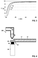
- a suitable glass shall be more than 80% transmissive at the wavelength of interest in the UV range as shown in Figure 3.
- Figure 3 depicts a chart indicating transmission (in percent) versus wavelength (in nm) of such glass as a function of glass thickness.
- T1 is a curve for a glass strip of 200 ⁇ m thickness
- T2 is a curve for a glass strip of 100 ⁇ m thickness
- T3 is a curve for a glass strip of 50 ⁇ m thickness.
- An example of a suitable glass is called "Corning Willow glass".
- Figure 4 illustrates schematically a process step during manufacture of an electronic device arrangement according to an embodiment of the invention.
- the polymide and adhesives overlaying the fixation points 50 at the perimeter 12 of the board 10 can be opened up using the same UV laser ablation system 200 used to drill vias in the printed circuit board 10, leaving behind the glass openings through which either UV laser or arc-lamps can illuminate the underlying adhesive resins 50.
- This is shown schematically in Figure 4 where a printed circuit board 10 is rigidly attached to a mechanical support as counterpart 30 via curing an adhesive resin dot as a UV curable adhesive 40 underneath a UV transparent element 20 coupled to the printed circuit board 10.
- An electronic device 100 can be manufactured by providing a printed circuit board arrangement comprising the printed circuit board 10 having at least one UV-transparent element 20 coupled to or integrated in the printed circuit board 10 for fixation of the printed circuit board 10 to a counterpart 30, dispensing a UV-curable adhesive 40 on the counterpart 30 and/or the UV-transparent element 20 in an area intended as interface 50 for fixation of the printed circuit board 10 and illuminating the UV-transparent element 20 with UV radiation and, thus, curing the UV-curable adhesive so that a rigid connection is established between the printed circuit board 10 and the counterpart 30 via the UV-transparent element 20.
- Figure 5 shows a flexible printed circuit board 10 folded around a mechanical frame as counterpart 30 that has one surface which is mounted to the printed circuit board 10, and the fixation is made with a window 22 as the UV-transparent element 20.
Landscapes
- Engineering & Computer Science (AREA)
- Microelectronics & Electronic Packaging (AREA)
- Chemical & Material Sciences (AREA)
- Inorganic Chemistry (AREA)
- Manufacturing & Machinery (AREA)
- Ceramic Engineering (AREA)
- Structure Of Printed Boards (AREA)
- Health & Medical Sciences (AREA)
- Biomedical Technology (AREA)
- Nuclear Medicine, Radiotherapy & Molecular Imaging (AREA)
- Radiology & Medical Imaging (AREA)
- Life Sciences & Earth Sciences (AREA)
- Animal Behavior & Ethology (AREA)
- General Health & Medical Sciences (AREA)
- Public Health (AREA)
- Veterinary Medicine (AREA)
- Prostheses (AREA)
Abstract
Description
- The invention relates to a printed circuit board arrangement and an electronic device having a printed circuit board arrangement, in particular an electronic device in an implantable medical device.
- As part of manufacturing inner assemblies for electronic devices, in particular electronic devices for medical implants which are intended to be implanted into a human or animal body, it is generally necessary to fixate the electronic printed circuit board (PCB) to mechanical support features in the assembly. This is necessary to ensure that the electronic device does not move around under normal use conditions including insertion into the device housing, thereby imparting stresses to the solder joints and components. These stresses can lead to cracks with crack growth ultimately leading to interconnect failures. Further, because of the very limited size of an implant the electronic device has to be significantly miniaturized thus leaving virtually no free real estate on the printed circuit board.
- Several approaches have been deployed over the years to achieve fixation of the circuit boards to mechanical support features, such as providing clips on the mechanical support frame to retain the circuit board, providing thermal staking of polymer pins from the support frame onto the circuit board, providing adhesive tapes (e.g. Polyimide tape) to retain the circuit board in position, and providing thermally cured adhesive resins to glue the PCB onto the support frame. Clips on the mechanical support requires complex mechanical support frame mold tool design (to form the clips) and use of substrate real estate to form "shelves" to provide counter-force to support the clip forces. Providing thermal or ultrasonic staking of polymer pins from the support frame onto the circuit board requires use of larger board real estate to capture the staking and for the staking tool to form the pin. This approach also uses high temperatures or vibrations in proximity to possibly sensitive components, such as multi-layer ceramic capacitors (MLCC). The use of adhesive tapes to retain the circuit board in position requires difficult tape handling and positioning operations and may not lead to firm retention of the printed circuit board in its intended position. The use of thermally cured adhesive resins to glue the PCB onto the support frame requires use of adhesive resins which generally have long cure/cooling cycle times of more than 10 minutes and high temperatures, up to 125°C, which can damage or warp other components, such as the polymer frames.
- It is an object of the invention to provide a printed circuit board arrangement for an electronic device having a printed circuit board which requires less real estate for fixation of the printed circuit board and does not require high temperatures or long cure times for fixation of the printed circuit board to a mechanical support.
- Another object of the invention is to provide an electronic device having a printed circuit board which requires less real estate for fixation of the printed circuit board and which does not require high temperatures for fixating of the printed circuit board to a mechanical support.
Another object of the invention is to provide a method for manufacturing such an electronic device. - The objects are achieved by the features of the independent claims. The other claims, the drawings, and the specification disclose advantageous embodiments of the invention.
- A printed circuit board arrangement is proposed comprising a printed circuit board, wherein at least one UV-transparent element is at least fixedly coupled to the printed circuit board, wherein the UV-transparent element is intended for fixation of the printed circuit board in an electronic device.
- The UV-transparent element may be an element separate from the printed circuit board which is attached to the printed circuit board or it may be integrated into the printed circuit board. The printed circuit board may be rigid or flexible.
- The printed circuit board is made of materials which are not transparent to ultraviolet radiation (UV radiation). Typically, polyimide is used for flexible printed circuit boards and glass filled adhesive resins are used in rigid printed circuit boards which are both nearly opaque in the UV range. Adhesive resins which are curable with ultraviolet radiation cannot be used for fixation of the printed circuit board, but by providing a UV-transparent element, adhesive resins become suitable for UV fixation of the printed circuit board.
- The inventive printed circuit board arrangement allows reduction of the required board real estate for fixation as well reduction of the temperatures and times required to form the fixation because curing can be effected by UV irradiation which is known to provide near instantaneous curing on properly formulated epoxies. This allows for economical manufacturing and facilitates the assembly of electronic devices which include such printed circuit board arrangements.
- According to a favorable embodiment, the UV-transparent element may be arranged along the perimeter of the printed circuit board. The perimeter is easy to access, and real estate required for the UV-transparent element on the printed circuit board is thereby minimized. Circuitry arranged in or on the printed circuit board remains undisturbed by the UV-transparent element.
- According to a favorable embodiment, the UV-transparent element may be made of glass. In particular, the UV-transparent element may have a thickness of not more than 200 µm, preferably not more than 100 µm, more preferably of not more than 50 µm. The UV-transparent element is stable and has a transmission for UV which is sufficient for curing resins beneath the UV-transparent element.
- According to another aspect of the invention, an electronic device is proposed, in particular an electronic device for a medical implant, comprising a printed circuit board, wherein at least one UV-transparent element is at least fixedly coupled to the printed circuit board in a position, which is intended as interface for fixation of the printed circuit board in the device.
- Advantageously, the design and construction of an electronic device is facilitated by the device comprising a flexible or rigid printed circuit board with UV-transparent elements or areas.
- A very fast and secure fixation process is enabled. By providing UV-transparent elements, UV-curable resins can be used for connecting the UV-transparent element to a counterpart. The fixation process requires only seconds for curing a UV-curable resin. This translates into lower manufacturing cost and cycle time during manufacture. The position of the printed circuit board in relation to the underlying fixation point on a mechanical feature such as a mechanical support or a frame can be maintained by appropriate process tooling.
- According to a favorable embodiment, the UV-transparent element may be a joining component between the printed circuit board and a counterpart, such as a mechanical support or a frame, to the printed circuit board for establishing a rigid connection between the printed circuit board and the counterpart.
- According to a favorable embodiment, a UV curable adhesive may be arranged between the UV-transparent element and the counterpart. In particular the UV curable adhesive may be an UV curable resin, preferably epoxy resin, polyurethane, acrylate polymer or silicone resin. This allows for a fast and accurate fixation process.
- The size of fixation features may be made very small, in particular having a diameter of only 75-200 µm, limited by the size of an ablation window in the printed circuit board. It is possible to make this window using the same ablation laser as is used for drilling vias into the printed circuit board during standard printed circuit board fabrication.
- Only a minimum dispense volume of adhesive resin is necessary, thereby reducing required substrate area required to accomplish fixation. This translates into size reduction of the final device design.
- According to a favorable embodiment, the UV-transparent element may be arranged along the perimeter of the printed circuit board. The perimeter is easily accessible during manufacture and valuable real estate of the printed circuit board is saved for the electronic circuitry on the board, and allowing use of fast curing UV epoxy resins to achieve retention of the printed circuit board to mechanical supports or frame features.
- In a further preferred embodiment, the UV-transparent element may be integrated into the printed circuit board. The printed circuit board may be rigid or flexible.
- According to a favorable embodiment, the UV-transparent element may be made of glass, preferably having a thickness of not more than 200 µm, preferably not more than 100 µm, more preferably of not more than 50 µm.
- According to another aspect of the invention, an implantable medical device is proposed, in particular an implantable leadless pacemaker, having an electronic device comprising a printed circuit board, wherein at least one UV-transparent element is at least fixedly coupled to the printed circuit board, wherein the UV-transparent element is intended for fixation of the printed circuit board in an electronic device.
- As part of manufacturing inner assemblies for such electronics, in particular medical electronics, it is generally necessary to fixate the electronic circuit board to mechanical support features in the assembly. Advantageously it can be ensured that the electronics are securely attached and do not move around under normal use conditions, which would impart stresses to the solder joints and components. By avoiding such stresses, damage to the implant such as cracks and crack growth ultimately leading to interconnect failures can be avoided.
- According to another aspect of the invention, a method for manufacturing an electronic device is proposed, with the steps of providing a printed circuit board arrangement comprising a printed circuit board having at least one UV-transparent element coupled to or integrated in the printed circuit board for fixation of the printed circuit board; providing a counterpart on which the printed circuit board is to be fixated; dispensing a UV-curable adhesive on the counterpart and/or the UV-transparent element in an area intended as interface for fixation of the printed circuit board; illuminating the UV-transparent element with UV radiation and curing the UV-curable adhesive.
- Advantageously, curing the UV-curable adhesive with an ablation laser, the ablation laser being used for drilling one or more vias in the printed circuit board.
- The present invention together with the above-mentioned and other objects and advantages may best be understood from the following detailed description of the embodiments, but not restricted to the embodiments, wherein is shown in:
- Fig. 1
- a plan view of a printed circuit board arrangement comprising a printed circuit board and a UV-transparent element at a perimeter of the printed circuit board according to an embodiment of the invention;
- Fig. 2
- a section view the of the printed circuit board arrangement along line II-II of
Figure 1 ; - Fig. 3
- a chart indicating transmission versus wavelength of commercially available glass as a function of glass thickness;
- Fig. 4
- schematically a process step during manufacture of an electronic device according to an embodiment of the invention; and
- Fig. 5
- an example embodiment of an electronic device comprising a flexible printed circuit board fixated to a mechanical frame.
- In the drawings, like elements are referred to with equal reference numerals. The drawings are merely schematic representations, not intended to portray specific parameters of the invention. Moreover, the drawings are intended to depict only typical embodiments of the invention and therefore should not be considered as limiting the scope of the invention.
-
Figures 1 and 2 depict in a plan view (Figure 1 ) and a section view (Figure 2 ) a printed circuit board arrangement according an embodiment of the invention. The printed circuit board arrangement comprises a printedcircuit board 10 and two UV-transparent elements 20 arranged at aperimeter 12 of the printedcircuit board 10. - The printed
circuit board 10 may be a standard printed circuit board with the UV-transparent elements 20 attached to theperimeter 12 or integrated into theperimeter 12. - A category of adhesive resins known as UV-curable adhesive resins have the desirable characteristics of nearly instantaneous curing when illuminated with ultraviolet light in the 320-380 nm range. By including a strip of very thin glass as UV-
transparent element 20, e.g. 50-75 µm thick, along theperimeter 12 of the printedcircuit board 10, the UV light required by such adhesive resins for catalyzing the curing process is able to reach the adhesive resin beneath the UV-transparent element 20. The UV-transparent element 20 may be included, for instance, during the board manufacturing. Example of these adhesive resins are epoxy resin, polyurethane, acrylate polymer or silicone resin. - A suitable glass shall be more than 80% transmissive at the wavelength of interest in the UV range as shown in
Figure 3. Figure 3 depicts a chart indicating transmission (in percent) versus wavelength (in nm) of such glass as a function of glass thickness. T1 is a curve for a glass strip of 200 µm thickness, T2 is a curve for a glass strip of 100 µm thickness, T3 is a curve for a glass strip of 50 µm thickness. An example of a suitable glass is called "Corning Willow glass". -
Figure 4 illustrates schematically a process step during manufacture of an electronic device arrangement according to an embodiment of the invention. During the manufacturing of the printedcircuit board 10, the polymide and adhesives overlaying the fixation points 50 at theperimeter 12 of theboard 10 can be opened up using the same UVlaser ablation system 200 used to drill vias in the printedcircuit board 10, leaving behind the glass openings through which either UV laser or arc-lamps can illuminate the underlying adhesive resins 50. This is shown schematically inFigure 4 where a printedcircuit board 10 is rigidly attached to a mechanical support ascounterpart 30 via curing an adhesive resin dot as a UVcurable adhesive 40 underneath a UVtransparent element 20 coupled to the printedcircuit board 10. - An
electronic device 100 can be manufactured by providing a printed circuit board arrangement comprising the printedcircuit board 10 having at least one UV-transparent element 20 coupled to or integrated in the printedcircuit board 10 for fixation of the printedcircuit board 10 to acounterpart 30, dispensing a UV-curable adhesive 40 on thecounterpart 30 and/or the UV-transparent element 20 in an area intended asinterface 50 for fixation of the printedcircuit board 10 and illuminating the UV-transparent element 20 with UV radiation and, thus, curing the UV-curable adhesive so that a rigid connection is established between the printedcircuit board 10 and thecounterpart 30 via the UV-transparent element 20. - The benefits of this approach for fixation on a miniaturized electronic assembly is shown schematically in
Figure 5 , which shows a flexible printedcircuit board 10 folded around a mechanical frame ascounterpart 30 that has one surface which is mounted to the printedcircuit board 10, and the fixation is made with a window 22 as the UV-transparent element 20.
Claims (13)
- A printed circuit board arrangement comprising a printed circuit board (10), wherein at least one UV-transparent element (20) is at least fixedly coupled to the printed circuit board (10), wherein the UV-transparent element (20) is intended for fixation of the printed circuit board (10) in an electronic device (100).
- The arrangement according to claim1, wherein the UV-transparent element (20) is arranged along the perimeter (12) of the printed circuit board (10).
- The arrangement according to claim 1 or 2, wherein the UV-transparent element (20) is integrated into the printed circuit board (10).
- The arrangement according to any one of the preceding claims, wherein the UV-transparent element (20) is made of glass, preferably wherein the UV-transparent element (20) has a thickness of not more than 200 µm, preferably not more than 100 µm, more preferably of not more than 50 µm.
- An electronic device (100), in particular an electronic device for a medical implant, comprising a printed circuit board (10), wherein at least one UV-transparent element (20) is at least fixedly coupled to the printed circuit board (10) in a position which is intended as interface (50) for fixation of the printed circuit board (10) in the device (100).
- The device according to claim 5, wherein the UV-transparent element (20) is a joining component between the printed circuit board (10) and a counterpart (30) to the printed circuit board (10) for establishing a rigid connection between the printed circuit board (10) and the counterpart (30).
- The device according to claim 5 or 6, wherein a UV curable adhesive (40) is arranged between the UV-transparent element (20) and the counterpart (30).
- The device according to claim 7, wherein the adhesive is a UV curable resin.
- The device according to any one of the claims 5 to 8, wherein the UV-transparent element (20) is arranged along the perimeter (12) of the printed circuit board (10).
- The device according to any one of the claims 5 to 9, wherein the UV-transparent element (20) is integrated into the printed circuit board (10).
- The device according to any one of the claims 5 to 10, wherein the UV-transparent element (20) is made of glass, preferably having a thickness of not more than 200 µm, preferably not more than 100 µm, more preferably of not more than 50 µm.
- An implantable medical device comprising an electronic device according to any one of the claims 5 to 11.
- A method for manufacturing an electronic device (100) according to any one of the claims 5 to 11, with the steps of- providing a printed circuit board arrangement comprising a printed circuit board (10) having at least one UV-transparent element (20) coupled to or integrated in the printed circuit board (10) in a position which is intended as interface (50) for fixation of the printed circuit board (10);- providing a counterpart (30) on which the printed circuit board (10) is to be fixated;- dispensing a UV-curable adhesive on the counterpart (30) and/or the UV-transparent element (20) in an area intended as interface (50) for fixation of the printed circuit board (10);- illuminating the UV-transparent element (20) with UV radiation and curing the UV-curable adhesive.
Applications Claiming Priority (1)
| Application Number | Priority Date | Filing Date | Title |
|---|---|---|---|
| US201562140456P | 2015-03-31 | 2015-03-31 |
Publications (3)
| Publication Number | Publication Date |
|---|---|
| EP3076768A2 true EP3076768A2 (en) | 2016-10-05 |
| EP3076768A3 EP3076768A3 (en) | 2016-10-19 |
| EP3076768B1 EP3076768B1 (en) | 2018-10-17 |
Family
ID=55628734
Family Applications (1)
| Application Number | Title | Priority Date | Filing Date |
|---|---|---|---|
| EP16160133.1A Active EP3076768B1 (en) | 2015-03-31 | 2016-03-14 | Printed circuit board arrangement and electronic device having a printed circuit board device |
Country Status (2)
| Country | Link |
|---|---|
| US (1) | US9992866B2 (en) |
| EP (1) | EP3076768B1 (en) |
Families Citing this family (1)
| Publication number | Priority date | Publication date | Assignee | Title |
|---|---|---|---|---|
| EP3603740A1 (en) * | 2018-08-02 | 2020-02-05 | BIOTRONIK SE & Co. KG | Implant |
Family Cites Families (3)
| Publication number | Priority date | Publication date | Assignee | Title |
|---|---|---|---|---|
| GB2189350B (en) | 1986-04-16 | 1989-11-29 | Marconi Electronic Devices | Electrical circuits |
| US10441185B2 (en) * | 2009-12-16 | 2019-10-15 | The Board Of Trustees Of The University Of Illinois | Flexible and stretchable electronic systems for epidermal electronics |
| TWI566663B (en) | 2011-03-15 | 2017-01-11 | 鴻海精密工業股份有限公司 | Latching assembly, working platform and circuit board fixing system using the same |
-
2016
- 2016-03-02 US US15/058,491 patent/US9992866B2/en active Active
- 2016-03-14 EP EP16160133.1A patent/EP3076768B1/en active Active
Non-Patent Citations (1)
| Title |
|---|
| None |
Also Published As
| Publication number | Publication date |
|---|---|
| EP3076768B1 (en) | 2018-10-17 |
| EP3076768A3 (en) | 2016-10-19 |
| US9992866B2 (en) | 2018-06-05 |
| US20160295693A1 (en) | 2016-10-06 |
Similar Documents
| Publication | Publication Date | Title |
|---|---|---|
| CN105452918B (en) | Optical module, installation method of optical module, optical module-mounted circuit board, optical module evaluation instrument system, circuit board, and communication system | |
| CN102046078B (en) | Catheter tip device and method for manufacturing same | |
| EP2008443B1 (en) | Method for assembling a camera module, and camera module | |
| CN113382670A (en) | Camera module, camera and cable connection method for camera module | |
| DE60109983T2 (en) | Chip-form electronic components, pseudo-wafers therefor, and methods of making same | |
| EP3186950B1 (en) | Imager module for a vehicle camera and method for the production thereof | |
| DE112010002709T5 (en) | IN VIVO QUERY DEVICE WITH FLEXIBLE PCB AND METHOD OF ASSEMBLING | |
| DE10023353A1 (en) | Optoelectronic component and method for producing it | |
| US20220236512A1 (en) | Optical sensor module | |
| JPS58111359A (en) | Integrated circuit device | |
| US9992866B2 (en) | Printed circuit board arrangement and electronic device having a printed circuit board device | |
| DE102009044714B4 (en) | Semiconductor device, semiconductor module and method for mounting the semiconductor device and for handling the semiconductor module | |
| van den Brand et al. | Flexible and stretchable electronics for wearable healthcare | |
| US20080184554A1 (en) | Mechanical assembly and electrical interconnection of the functional components of an active implantable medical device | |
| EP1503412A2 (en) | Semiconductor device and manufacturing method of the same | |
| DE3739333A1 (en) | Process for producing bonded joints by means of a laser | |
| DE10133361C2 (en) | Process for the production of packaging for semiconductor chips | |
| US20050113869A1 (en) | Armed suture with adhesively attached surgical needle | |
| DE102015205051A1 (en) | Electronic module with alpha radiation protection for a transmission control unit and transmission control unit | |
| Szabo et al. | Irreversible, self-aligned microfluidic packaging for chronic implant applications | |
| JP6064440B2 (en) | Electronic device, method for manufacturing electronic device, and unit testing method for electronic component | |
| US6312962B1 (en) | Method for COB mounting of electronic chips on a circuit board | |
| DE10120928C1 (en) | Production of contact joint between semiconductor chip and substrate comprises applying hardenable conducting adhesive on contact surfaces of substrate and chip, joining, and hardening adhesive to form contact joint | |
| US11904073B2 (en) | Biocompatible electromechanical connection for ceramic substrate electronics for biomedical implant | |
| US20070134974A1 (en) | Housing for a medical implant |
Legal Events
| Date | Code | Title | Description |
|---|---|---|---|
| PUAI | Public reference made under article 153(3) epc to a published international application that has entered the european phase |
Free format text: ORIGINAL CODE: 0009012 |
|
| PUAL | Search report despatched |
Free format text: ORIGINAL CODE: 0009013 |
|
| AK | Designated contracting states |
Kind code of ref document: A2 Designated state(s): AL AT BE BG CH CY CZ DE DK EE ES FI FR GB GR HR HU IE IS IT LI LT LU LV MC MK MT NL NO PL PT RO RS SE SI SK SM TR |
|
| AX | Request for extension of the european patent |
Extension state: BA ME |
|
| AK | Designated contracting states |
Kind code of ref document: A3 Designated state(s): AL AT BE BG CH CY CZ DE DK EE ES FI FR GB GR HR HU IE IS IT LI LT LU LV MC MK MT NL NO PL PT RO RS SE SI SK SM TR |
|
| AX | Request for extension of the european patent |
Extension state: BA ME |
|
| RIC1 | Information provided on ipc code assigned before grant |
Ipc: H05K 1/02 20060101AFI20160914BHEP Ipc: H05K 3/00 20060101ALI20160914BHEP |
|
| STAA | Information on the status of an ep patent application or granted ep patent |
Free format text: STATUS: REQUEST FOR EXAMINATION WAS MADE |
|
| 17P | Request for examination filed |
Effective date: 20170410 |
|
| RBV | Designated contracting states (corrected) |
Designated state(s): AL AT BE BG CH CY CZ DE DK EE ES FI FR GB GR HR HU IE IS IT LI LT LU LV MC MK MT NL NO PL PT RO RS SE SI SK SM TR |
|
| REG | Reference to a national code |
Ref country code: DE Ref legal event code: R079 Ref document number: 602016006353 Country of ref document: DE Free format text: PREVIOUS MAIN CLASS: H05K0001020000 Ipc: A61N0001375000 |
|
| GRAP | Despatch of communication of intention to grant a patent |
Free format text: ORIGINAL CODE: EPIDOSNIGR1 |
|
| STAA | Information on the status of an ep patent application or granted ep patent |
Free format text: STATUS: GRANT OF PATENT IS INTENDED |
|
| RIC1 | Information provided on ipc code assigned before grant |
Ipc: A61N 1/375 20060101AFI20180425BHEP Ipc: H05K 1/02 20060101ALI20180425BHEP |
|
| INTG | Intention to grant announced |
Effective date: 20180516 |
|
| GRAS | Grant fee paid |
Free format text: ORIGINAL CODE: EPIDOSNIGR3 |
|
| GRAA | (expected) grant |
Free format text: ORIGINAL CODE: 0009210 |
|
| STAA | Information on the status of an ep patent application or granted ep patent |
Free format text: STATUS: THE PATENT HAS BEEN GRANTED |
|
| AK | Designated contracting states |
Kind code of ref document: B1 Designated state(s): AL AT BE BG CH CY CZ DE DK EE ES FI FR GB GR HR HU IE IS IT LI LT LU LV MC MK MT NL NO PL PT RO RS SE SI SK SM TR |
|
| REG | Reference to a national code |
Ref country code: GB Ref legal event code: FG4D |
|
| REG | Reference to a national code |
Ref country code: CH Ref legal event code: EP |
|
| REG | Reference to a national code |
Ref country code: IE Ref legal event code: FG4D |
|
| REG | Reference to a national code |
Ref country code: DE Ref legal event code: R096 Ref document number: 602016006353 Country of ref document: DE Ref country code: AT Ref legal event code: REF Ref document number: 1053289 Country of ref document: AT Kind code of ref document: T Effective date: 20181115 |
|
| REG | Reference to a national code |
Ref country code: NL Ref legal event code: MP Effective date: 20181017 |
|
| REG | Reference to a national code |
Ref country code: LT Ref legal event code: MG4D |
|
| REG | Reference to a national code |
Ref country code: AT Ref legal event code: MK05 Ref document number: 1053289 Country of ref document: AT Kind code of ref document: T Effective date: 20181017 |
|
| PG25 | Lapsed in a contracting state [announced via postgrant information from national office to epo] |
Ref country code: NL Free format text: LAPSE BECAUSE OF FAILURE TO SUBMIT A TRANSLATION OF THE DESCRIPTION OR TO PAY THE FEE WITHIN THE PRESCRIBED TIME-LIMIT Effective date: 20181017 |
|
| PG25 | Lapsed in a contracting state [announced via postgrant information from national office to epo] |
Ref country code: ES Free format text: LAPSE BECAUSE OF FAILURE TO SUBMIT A TRANSLATION OF THE DESCRIPTION OR TO PAY THE FEE WITHIN THE PRESCRIBED TIME-LIMIT Effective date: 20181017 Ref country code: LV Free format text: LAPSE BECAUSE OF FAILURE TO SUBMIT A TRANSLATION OF THE DESCRIPTION OR TO PAY THE FEE WITHIN THE PRESCRIBED TIME-LIMIT Effective date: 20181017 Ref country code: HR Free format text: LAPSE BECAUSE OF FAILURE TO SUBMIT A TRANSLATION OF THE DESCRIPTION OR TO PAY THE FEE WITHIN THE PRESCRIBED TIME-LIMIT Effective date: 20181017 Ref country code: LT Free format text: LAPSE BECAUSE OF FAILURE TO SUBMIT A TRANSLATION OF THE DESCRIPTION OR TO PAY THE FEE WITHIN THE PRESCRIBED TIME-LIMIT Effective date: 20181017 Ref country code: BG Free format text: LAPSE BECAUSE OF FAILURE TO SUBMIT A TRANSLATION OF THE DESCRIPTION OR TO PAY THE FEE WITHIN THE PRESCRIBED TIME-LIMIT Effective date: 20190117 Ref country code: PL Free format text: LAPSE BECAUSE OF FAILURE TO SUBMIT A TRANSLATION OF THE DESCRIPTION OR TO PAY THE FEE WITHIN THE PRESCRIBED TIME-LIMIT Effective date: 20181017 Ref country code: FI Free format text: LAPSE BECAUSE OF FAILURE TO SUBMIT A TRANSLATION OF THE DESCRIPTION OR TO PAY THE FEE WITHIN THE PRESCRIBED TIME-LIMIT Effective date: 20181017 Ref country code: NO Free format text: LAPSE BECAUSE OF FAILURE TO SUBMIT A TRANSLATION OF THE DESCRIPTION OR TO PAY THE FEE WITHIN THE PRESCRIBED TIME-LIMIT Effective date: 20190117 Ref country code: IS Free format text: LAPSE BECAUSE OF FAILURE TO SUBMIT A TRANSLATION OF THE DESCRIPTION OR TO PAY THE FEE WITHIN THE PRESCRIBED TIME-LIMIT Effective date: 20190217 Ref country code: AT Free format text: LAPSE BECAUSE OF FAILURE TO SUBMIT A TRANSLATION OF THE DESCRIPTION OR TO PAY THE FEE WITHIN THE PRESCRIBED TIME-LIMIT Effective date: 20181017 |
|
| PG25 | Lapsed in a contracting state [announced via postgrant information from national office to epo] |
Ref country code: RS Free format text: LAPSE BECAUSE OF FAILURE TO SUBMIT A TRANSLATION OF THE DESCRIPTION OR TO PAY THE FEE WITHIN THE PRESCRIBED TIME-LIMIT Effective date: 20181017 Ref country code: GR Free format text: LAPSE BECAUSE OF FAILURE TO SUBMIT A TRANSLATION OF THE DESCRIPTION OR TO PAY THE FEE WITHIN THE PRESCRIBED TIME-LIMIT Effective date: 20190118 Ref country code: SE Free format text: LAPSE BECAUSE OF FAILURE TO SUBMIT A TRANSLATION OF THE DESCRIPTION OR TO PAY THE FEE WITHIN THE PRESCRIBED TIME-LIMIT Effective date: 20181017 Ref country code: AL Free format text: LAPSE BECAUSE OF FAILURE TO SUBMIT A TRANSLATION OF THE DESCRIPTION OR TO PAY THE FEE WITHIN THE PRESCRIBED TIME-LIMIT Effective date: 20181017 Ref country code: PT Free format text: LAPSE BECAUSE OF FAILURE TO SUBMIT A TRANSLATION OF THE DESCRIPTION OR TO PAY THE FEE WITHIN THE PRESCRIBED TIME-LIMIT Effective date: 20190217 |
|
| REG | Reference to a national code |
Ref country code: DE Ref legal event code: R097 Ref document number: 602016006353 Country of ref document: DE |
|
| PG25 | Lapsed in a contracting state [announced via postgrant information from national office to epo] |
Ref country code: DK Free format text: LAPSE BECAUSE OF FAILURE TO SUBMIT A TRANSLATION OF THE DESCRIPTION OR TO PAY THE FEE WITHIN THE PRESCRIBED TIME-LIMIT Effective date: 20181017 Ref country code: IT Free format text: LAPSE BECAUSE OF FAILURE TO SUBMIT A TRANSLATION OF THE DESCRIPTION OR TO PAY THE FEE WITHIN THE PRESCRIBED TIME-LIMIT Effective date: 20181017 Ref country code: CZ Free format text: LAPSE BECAUSE OF FAILURE TO SUBMIT A TRANSLATION OF THE DESCRIPTION OR TO PAY THE FEE WITHIN THE PRESCRIBED TIME-LIMIT Effective date: 20181017 |
|
| PLBE | No opposition filed within time limit |
Free format text: ORIGINAL CODE: 0009261 |
|
| STAA | Information on the status of an ep patent application or granted ep patent |
Free format text: STATUS: NO OPPOSITION FILED WITHIN TIME LIMIT |
|
| PG25 | Lapsed in a contracting state [announced via postgrant information from national office to epo] |
Ref country code: RO Free format text: LAPSE BECAUSE OF FAILURE TO SUBMIT A TRANSLATION OF THE DESCRIPTION OR TO PAY THE FEE WITHIN THE PRESCRIBED TIME-LIMIT Effective date: 20181017 Ref country code: SK Free format text: LAPSE BECAUSE OF FAILURE TO SUBMIT A TRANSLATION OF THE DESCRIPTION OR TO PAY THE FEE WITHIN THE PRESCRIBED TIME-LIMIT Effective date: 20181017 Ref country code: SM Free format text: LAPSE BECAUSE OF FAILURE TO SUBMIT A TRANSLATION OF THE DESCRIPTION OR TO PAY THE FEE WITHIN THE PRESCRIBED TIME-LIMIT Effective date: 20181017 Ref country code: EE Free format text: LAPSE BECAUSE OF FAILURE TO SUBMIT A TRANSLATION OF THE DESCRIPTION OR TO PAY THE FEE WITHIN THE PRESCRIBED TIME-LIMIT Effective date: 20181017 |
|
| 26N | No opposition filed |
Effective date: 20190718 |
|
| PG25 | Lapsed in a contracting state [announced via postgrant information from national office to epo] |
Ref country code: SI Free format text: LAPSE BECAUSE OF FAILURE TO SUBMIT A TRANSLATION OF THE DESCRIPTION OR TO PAY THE FEE WITHIN THE PRESCRIBED TIME-LIMIT Effective date: 20181017 Ref country code: MC Free format text: LAPSE BECAUSE OF FAILURE TO SUBMIT A TRANSLATION OF THE DESCRIPTION OR TO PAY THE FEE WITHIN THE PRESCRIBED TIME-LIMIT Effective date: 20181017 |
|
| PG25 | Lapsed in a contracting state [announced via postgrant information from national office to epo] |
Ref country code: LU Free format text: LAPSE BECAUSE OF NON-PAYMENT OF DUE FEES Effective date: 20190314 |
|
| REG | Reference to a national code |
Ref country code: BE Ref legal event code: MM Effective date: 20190331 |
|
| PG25 | Lapsed in a contracting state [announced via postgrant information from national office to epo] |
Ref country code: FR Free format text: LAPSE BECAUSE OF NON-PAYMENT OF DUE FEES Effective date: 20190331 Ref country code: BE Free format text: LAPSE BECAUSE OF NON-PAYMENT OF DUE FEES Effective date: 20190331 |
|
| PG25 | Lapsed in a contracting state [announced via postgrant information from national office to epo] |
Ref country code: TR Free format text: LAPSE BECAUSE OF FAILURE TO SUBMIT A TRANSLATION OF THE DESCRIPTION OR TO PAY THE FEE WITHIN THE PRESCRIBED TIME-LIMIT Effective date: 20181017 |
|
| PG25 | Lapsed in a contracting state [announced via postgrant information from national office to epo] |
Ref country code: MT Free format text: LAPSE BECAUSE OF NON-PAYMENT OF DUE FEES Effective date: 20190314 |
|
| GBPC | Gb: european patent ceased through non-payment of renewal fee |
Effective date: 20200314 |
|
| PG25 | Lapsed in a contracting state [announced via postgrant information from national office to epo] |
Ref country code: GB Free format text: LAPSE BECAUSE OF NON-PAYMENT OF DUE FEES Effective date: 20200314 |
|
| PG25 | Lapsed in a contracting state [announced via postgrant information from national office to epo] |
Ref country code: CY Free format text: LAPSE BECAUSE OF FAILURE TO SUBMIT A TRANSLATION OF THE DESCRIPTION OR TO PAY THE FEE WITHIN THE PRESCRIBED TIME-LIMIT Effective date: 20181017 |
|
| PG25 | Lapsed in a contracting state [announced via postgrant information from national office to epo] |
Ref country code: HU Free format text: LAPSE BECAUSE OF FAILURE TO SUBMIT A TRANSLATION OF THE DESCRIPTION OR TO PAY THE FEE WITHIN THE PRESCRIBED TIME-LIMIT; INVALID AB INITIO Effective date: 20160314 |
|
| PG25 | Lapsed in a contracting state [announced via postgrant information from national office to epo] |
Ref country code: MK Free format text: LAPSE BECAUSE OF FAILURE TO SUBMIT A TRANSLATION OF THE DESCRIPTION OR TO PAY THE FEE WITHIN THE PRESCRIBED TIME-LIMIT Effective date: 20181017 |
|
| P01 | Opt-out of the competence of the unified patent court (upc) registered |
Effective date: 20230613 |
|
| REG | Reference to a national code |
Ref country code: CH Ref legal event code: U11 Free format text: ST27 STATUS EVENT CODE: U-0-0-U10-U11 (AS PROVIDED BY THE NATIONAL OFFICE) Effective date: 20260401 |
|
| PGFP | Annual fee paid to national office [announced via postgrant information from national office to epo] |
Ref country code: DE Payment date: 20260320 Year of fee payment: 11 Ref country code: IE Payment date: 20260323 Year of fee payment: 11 |
|
| PGFP | Annual fee paid to national office [announced via postgrant information from national office to epo] |
Ref country code: CH Payment date: 20260401 Year of fee payment: 11 |