EP3076514A1 - A method and system for high-speed power source transfer (hs-pst) - Google Patents
A method and system for high-speed power source transfer (hs-pst) Download PDFInfo
- Publication number
- EP3076514A1 EP3076514A1 EP16161975.4A EP16161975A EP3076514A1 EP 3076514 A1 EP3076514 A1 EP 3076514A1 EP 16161975 A EP16161975 A EP 16161975A EP 3076514 A1 EP3076514 A1 EP 3076514A1
- Authority
- EP
- European Patent Office
- Prior art keywords
- load bus
- source
- frequency
- value
- alternate source
- Prior art date
- Legal status (The legal status is an assumption and is not a legal conclusion. Google has not performed a legal analysis and makes no representation as to the accuracy of the status listed.)
- Granted
Links
Images


Classifications
-
- H—ELECTRICITY
- H02—GENERATION; CONVERSION OR DISTRIBUTION OF ELECTRIC POWER
- H02J—ELECTRIC POWER NETWORKS; CIRCUIT ARRANGEMENTS OR SYSTEMS FOR SUPPLYING OR DISTRIBUTING ELECTRIC POWER; SYSTEMS FOR STORING ELECTRIC ENERGY
- H02J9/00—Circuit arrangements for emergency or stand-by power supply, e.g. for emergency lighting
- H02J9/04—Circuit arrangements for emergency or stand-by power supply, e.g. for emergency lighting in which the distribution system is disconnected from the normal source and connected to a standby source
- H02J9/06—Circuit arrangements for emergency or stand-by power supply, e.g. for emergency lighting in which the distribution system is disconnected from the normal source and connected to a standby source with automatic change-over, e.g. UPS systems
- H02J9/061—Circuit arrangements for emergency or stand-by power supply, e.g. for emergency lighting in which the distribution system is disconnected from the normal source and connected to a standby source with automatic change-over, e.g. UPS systems for DC powered loads
-
- G—PHYSICS
- G01—MEASURING; TESTING
- G01R—MEASURING ELECTRIC VARIABLES; MEASURING MAGNETIC VARIABLES
- G01R21/00—Arrangements for measuring electric power or power factor
- G01R21/133—Arrangements for measuring electric power or power factor by using digital technique
-
- H—ELECTRICITY
- H02—GENERATION; CONVERSION OR DISTRIBUTION OF ELECTRIC POWER
- H02J—ELECTRIC POWER NETWORKS; CIRCUIT ARRANGEMENTS OR SYSTEMS FOR SUPPLYING OR DISTRIBUTING ELECTRIC POWER; SYSTEMS FOR STORING ELECTRIC ENERGY
- H02J3/00—Circuit arrangements for AC mains or AC distribution networks
- H02J3/007—Arrangements for selectively connecting one or more loads to one or more power sources or power lines
-
- H—ELECTRICITY
- H02—GENERATION; CONVERSION OR DISTRIBUTION OF ELECTRIC POWER
- H02J—ELECTRIC POWER NETWORKS; CIRCUIT ARRANGEMENTS OR SYSTEMS FOR SUPPLYING OR DISTRIBUTING ELECTRIC POWER; SYSTEMS FOR STORING ELECTRIC ENERGY
- H02J3/00—Circuit arrangements for AC mains or AC distribution networks
- H02J3/04—Arrangements for connecting networks of the same frequency but supplied from different sources
- H02J3/08—Synchronisation of networks
-
- H—ELECTRICITY
- H02—GENERATION; CONVERSION OR DISTRIBUTION OF ELECTRIC POWER
- H02J—ELECTRIC POWER NETWORKS; CIRCUIT ARRANGEMENTS OR SYSTEMS FOR SUPPLYING OR DISTRIBUTING ELECTRIC POWER; SYSTEMS FOR STORING ELECTRIC ENERGY
- H02J9/00—Circuit arrangements for emergency or stand-by power supply, e.g. for emergency lighting
- H02J9/04—Circuit arrangements for emergency or stand-by power supply, e.g. for emergency lighting in which the distribution system is disconnected from the normal source and connected to a standby source
- H02J9/06—Circuit arrangements for emergency or stand-by power supply, e.g. for emergency lighting in which the distribution system is disconnected from the normal source and connected to a standby source with automatic change-over, e.g. UPS systems
- H02J9/068—Electronic means for switching from one power supply to another power supply, e.g. to avoid parallel connection
-
- Y—GENERAL TAGGING OF NEW TECHNOLOGICAL DEVELOPMENTS; GENERAL TAGGING OF CROSS-SECTIONAL TECHNOLOGIES SPANNING OVER SEVERAL SECTIONS OF THE IPC; TECHNICAL SUBJECTS COVERED BY FORMER USPC CROSS-REFERENCE ART COLLECTIONS [XRACs] AND DIGESTS
- Y02—TECHNOLOGIES OR APPLICATIONS FOR MITIGATION OR ADAPTATION AGAINST CLIMATE CHANGE
- Y02E—REDUCTION OF GREENHOUSE GAS [GHG] EMISSIONS, RELATED TO ENERGY GENERATION, TRANSMISSION OR DISTRIBUTION
- Y02E40/00—Technologies for an efficient electrical power generation, transmission or distribution
- Y02E40/10—Flexible AC transmission systems [FACTS]
Definitions
- the present disclosure relates generally to power source transfer. More specifically, the present disclosure relates to a high-speed power source transfer system that helps maintain power continuity to loads.
- the primary power source and the alternative power source may each include a circuit breaker that can connect/disconnect the power source from the loads on the load bus.
- a high-speed power source transfer (HS-PST) system controls which power source (e.g., the primary power source or the alternative power source) is powering the loads on the load bus. If, for example, the primary power source loses power, the HS-PST system can quickly change to the alternative power source.
- HS-PST high-speed power source transfer
- an electronic device configured to switchover power supplied from a primary source to an alternate source to maintain continuity of power supplied to a load bus.
- the electronic device includes one or more processors configured to identify availability of the alternate source using source monitoring in order to measure and calculate a tracking frequency for controlling a variable sampling interval of the one or more processors.
- the one or more processors are configured to obtain signal samples having associated time stamps from the primary source, the alternate source, and the load bus.
- the one or more processors store load bus signal samples and associated time stamps of the load bus into a variable length buffer.
- the one or more processors calculate a new time stamp for transferring to a fixed length buffer from a measured load bus signal frequency for applying a dual buffer sampling interval transfer to estimate a new sample value at the calculated new time stamp. In some embodiments, the one or more processors store the new sample value and associated new time stamp into the fixed length buffer.
- the one or more processors determine a set of attributes from samples of the alternate source using the tracking frequency and fixed length buffer samples of a load bus supply, wherein the set of attributes comprise a magnitude, an angle, a frequency, a slip, an acceleration, or any combination thereof, and calculate supervising conditions to execute a source switchover signal when the primary source is unavailable based at least in part on comparing the set of load bus attributes to alternate source attributes at an estimated instance of switchover.
- a non-transitory computer-readable medium includes stored instructions thereon.
- the instructions are configured to be executed by an electronic device that is configured to switchover power supplied from a primary source to an alternate source to maintain continuity of power supplied to a load bus.
- the instructions are configured to identify availability of the alternate source using source monitoring in order to measure and calculate a tracking frequency for controlling a variable sampling interval of one or more processors.
- the instructions are configured to obtain signal samples having associated time stamps from the primary source, the alternate source, and the load bus.
- the instructions are configured to store load bus signal samples and associated time stamps of the load bus into a variable length buffer.
- the instructions are configured to calculate a new time stamp for transferring to a fixed length buffer from a measured load bus signal frequency for applying a dual buffer sampling interval transfer to estimate a new sample value at the calculated new time stamp.
- the instructions are configured to store the new sample value and associated new time stamp into the fixed length buffer, determine a set of attributes from samples of the alternate source using the tracking frequency and fixed length buffer samples of a load bus supply, wherein the set of attributes comprise a magnitude, an angle, a frequency, a slip, an acceleration, or any combination thereof, and calculate supervising conditions to execute a source switchover signal when the primary source is unavailable based at least in part on comparing the set of load bus attributes to alternate source attributes at an estimated instance of switchover.
- an electronic device includes a processor, wherein the processor is configured to measure event attributes associated with a first switchover initiation event, wherein a signal is received from a primary source, an alternative source, a load bus, or any combination thereof, wherein the switchover initiation event comprises switching over power delivered to a load on a load bus from the primary source to the alternative source, determine an update by comparing the event attributes measurement to initial settings, wherein the update is related to the load bus and the alternative source during a second switchover event, wherein the comparison to a magnitude, a phase, a frequency, a slip, an acceleration, or any combination thereof of the alternative source or the load bus, and supervising conditions, and generate a notification that provides recommendations for a device configuration update.
- a motor on the load bus may have a load connected to a shaft that rotates based on power attributes of the primary power source (e.g., voltage, phase, frequency). As the shaft rotates, the shaft builds/keeps inertia.
- the primary power source fails, the power attributes of the primary power source and/or the load bus may not be synchronized with the alternative source (e.g., the primary source and alternative source may operate independently from each other). For instance, the load bus may lead the alternative source in phase by twenty degrees.
- the HS-PST may change to the alternative power source after the load bus phase more closely aligns with the phase of the alternative power source (e.g., within 5 degrees of each other). As such, it is desirable to address transferring between sources in such a way that the processes (e.g., motors) on the load bus are uninterrupted.
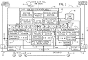
- FIG. 1 is a schematic diagram of a system 10 using a high-speed power source transfer (HS-PST) system 12.
- the system 10 includes a primary source (PS) 14 and an alternative source 16 (AS) selectively electrically coupled to loads on a load bus 18 (LB), such as, for instance, induction and/or synchronous motors 20.
- PS primary source
- AS alternative source 16
- LB load bus 18
- the PS 14 includes a PS circuit breaker 22
- the AS 16 includes an AS circuit breaker 24.
- the PS circuit breaker 22 is closed, thereby enabling the PS 14 to supply power to the loads on the LB 18. Under these conditions, the AS circuit breaker 24 is open. If the PS 14 fails, it may be desirable to transfer power sources from the PS 14 to the AS 16 by closing the AS circuit breaker 24 and opening the PS circuit breaker 22, thereby powering the loads on the LB 18 with the AS 16. That is, the HS-PST system 12 may be configured to switchover power supplied from the PS 14 to the AS 16 to maintain continuity of power supplied to the LB 18.
- the HS-PST 12 may be used to communicate open and/or close signals with the PS circuit breaker 22 and the AS circuit breaker 24.
- a high speed synchronizer 26 of the HS-PST system 12 may provide control execution 28 configured to communicate open and/or close signals with the PS circuit breaker 22 and the AS circuit breaker 24 via contact I/O modules 30 of the high speed synchronizer 26.
- the HS-PST system 12 may process signals received from the PS 14, AS 16, and LB 18. For instance, a PS voltage transformer 32, a LB voltage transformer 34, and an AS voltage transformer 36 may provide galvanic isolation (e.g., used to isolate where two or more circuits need to communicate with a device, such as the HS-PST system 12, and the circuits may be at different grounds) and enable the HS-PST system 12 to receive signals related to the health of the sources and bus.
- galvanic isolation e.g., used to isolate where two or more circuits need to communicate with a device, such as the HS-PST system 12, and the circuits may be at different grounds
- the HS-PST 12 may include a PS signal processor 38, a LB signal processor 40, and an AS signal processor 42.
- the PS signal processor 38, LB signal processor 40, and the AS signal processor 42 may process signals received from the PS 14, the LB 18, and the AS 16 respectively.
- each processing sub-system may receive signals relating to the health of the sources and bus.
- the high speed synchronizer 26, the PS signal processor 38, the LB signal processor 40, and the AS signal processor 42 each may include a processor or multiple processors, memory, and inputs/outputs. While the systems are depicted as separate systems, alternatively, sub-systems may share a processor or multiple processors and/or memory.
- the processor(s) may be operatively coupled to the memory to execute instructions for carrying out the presently disclosed techniques. These instructions may be encoded in programs and stored in a tangible non-transitory computer-readable medium, such as the memory and/or other storage.
- the processor may be a general purpose processor, system-on-chip (SoC) device, or application specific integrated circuit, or some other processor configuration.
- Memory in the embodiment, includes a computer readable medium, such as, without limitation, a hard disk drive, a solid state drive, a diskette, a flash drive, a compact disc, a digital video disc, random access memory (RAM), and/or any suitable storage device that enables the processor(s) to store, retrieve, and/or execute instructions and/or data.
- Memory may include one or more local and/or remote storage devices.
- FIG. 1 shows the contact I/O modules 30 as a part of the high-speed power source transfer system 12
- the contact I/O modules 30 may be separate from the HS-PST system 12.
- the contact I/O modules 30 may communicate with any suitable wired or wireless communication protocol.
- the I/O modules 30 may connect to a network using, for example, a wired Ethernet protocol or a wireless Ethernet protocol.
- the high speed synchronizer 26 may communicate with a workstation 43 using any suitable protocol (e.g., wireless or wired protocol).
- the workstation 43 may allow an operator to configure the high speed synchronizer to the specific set up where the high speed synchronizer is being used. For instance, the workstation 43 may allow the user to specify details about the motors 20 on the LB 18, details about the circuit breakers (e.g., open/close time), details about threshold values used to detect when transfer should take place, or the like. Further, the high speed synchronizer 26 may communicate updates or potential changes to the instructions stored on the high speed synchronizer 26.
- the PS signal processor 38 may receive input signals that provide an indication of primary source 14 power attribute values.
- the input signals may be conditioned 44 (e.g., filtered, amplified, isolated, etc.), converted to digital values using sample-hold and analog-to-digital conversion 46 (S/H & ADC) techniques, processed using, for example, digital signal processing 48 (DSP), and/or estimated using signal parameter estimation 50.
- the PS signal processor 38 may determine power attribute values, such as a PS voltage magnitude value 56, PS phase value 58, PS frequency value 60, PS slip value 62, and PS acceleration value 64 (e.g., rate of change of the primary source slip value 62). Once the PS voltage magnitude value 56, PS phase value 58, PS frequency value 60, PS slip value 62, and PS acceleration value 64 are determined, the PS signal processor 38 may transmit an indication of the primary source power attribute values to the high speed synchronizer 26.
- the LB signal processor 40 may receive input signals that provide an indication of the LB 18 power attribute values.
- the input signals received by the LB signal processor 40 may be conditioned 44 (e.g., filtered, amplified, isolated, etc.), converted to digital values using sample-hold and analog-to-digital conversion 46 (S/H & ADC) techniques, processed using, for example, digital signal processing 48 (DSP), and/or estimated using signal parameter estimation 50.
- the LB signal processor 40 may determine power attribute values, such as a LB voltage magnitude value 66, LB voltage phase value 68, LB frequency value 70, LB slip value 72, and a LB acceleration value 74 (e.g., rate of change of the LB slip value 72).
- the LB signal processor 40 may receive the frequency from the remaining healthy bus. As further described below, the LB signal processor 40 may perform dual buffer sampling interval transfer 52 by tracking the AS frequency. Once the power attribute values are determined, the values may be sent to the high speed synchronizer 26.
- the magnitude of LB signals use a Root-Mean-Square (RMS) value, and the magnitude of the primary and auxiliary supply uses non-recursive full cycle Discrete Fourier Transform (DFT).
- one or more processors of the HS-PST system 12 may be configured to calculate the angle (e.g., LB phase value 68) of the LB 18 by utilizing a rotationary recursive Discrete Fourier Transform
- the AS signal processor 42 may receive input signals that provide an indication of AS power attribute values.
- the input signals received by the AS signal processor 42 may be conditioned 44 (e.g., filtered, amplified, isolated, etc.), converted to digital values using sample-hold and analog-to-digital conversion 46 (S/H & ADC) techniques, processed using, for example, digital signal processing 48 (DSP), and/or estimated using signal parameter estimation 50.
- the AS signal processor 42 may determine power attribute values, such as an AS voltage magnitude value 76, AS phase value 78, AS frequency value 80, AS slip value 82, and an AS acceleration value 84 (e.g., rate of change of the AS slip value 82). Once the power attribute values are determined, the values may be sent to the high speed synchronizer 26.
- one or more processors may be configured to calculate a first derivative of the measured frequency 60, 70, 80 as the slip.
- the one or more processors may be configured to calculate a second derivative of the measured frequency 60, 70, 80 as the acceleration 64, 74, 84.
- Frequency tracking (Ftrack) 54 may be obtained from the remaining healthy source (e.g., the AS 16). Frequency tracking is used to resample the LB data at the rate of, for example, the AS frequency 80. As further explained below, frequency tracking 54 on the remaining healthy source may enable measurement of the LB voltage magnitude value 66, LB voltage phase value 68, LB frequency value 70, LB slip value 72, and LB acceleration value 74.
- the AS 16 may power the LB 18.
- the system may transfer back to the PS 14 or continue to receive power from the AS 16. If power is not transferred, eventually the AS 16 may fail and it is desirable to transfer to the PS 14.
- the PS signal processor 38 may obtain the Ftrack using the PS 14 (e.g., the healthy source).
- adaptive least error square may be used with a look up table of coefficients to calculate LB voltage phase properly. As such, any suitable method may be used to determine the LB power attribute values.
- the high-speed synchronizer 26 may include a processor or processors operatively coupled to memory that enables the processor to store, retrieve, and/or execute instructions and/or data.
- the high-speed synchronizer may include a tangible non-transitory computer-readable medium having stored instructions thereon.
- the high-speed synchronizer may include instructions (e.g., software) and/or hardware to perform control execution 28, continuous source monitoring 86, synchronizer predictions 88, high-speed synchrochecks 90, resultant V/Hz monitoring 92, and event parameter estimation & archiving 94.
- Continuous source monitoring 86 may include monitoring the PS 14, AS 16, and LB 18 for any signs of failures.
- the source monitoring 86 comprises continuously monitoring voltage magnitude, frequency, and power quality of the AS 16 within a specified range.
- One or more of the processors may be configured to identify availability of the AS 16 using source monitoring 86 in order to measure and calculate a tracking frequency (e.g., Ftrack 54) for controlling a variable sampling interval of the one or more processors.
- the one or more processors may obtain signal samples having associated time stamps from the PS 14, the AS 16, and the LB 18, and/or store LB signal samples and associated time stamps of the LB into a variable length buffer (shown in FIG. 5 as buffer 104).
- the one or more processor may then store the new sample value and associated new time stamp into the fixed length buffer (shown in FIG. 5 as buffer 108).
- the one or more processors may determine a set of power attributes from samples of the AS 16 using the tracking frequency (e.g., Ftrack 54) and fixed length buffer samples of a LB supply, wherein the set of power attributes comprises a magnitude(e.g., voltage magnitude value 56, 66, 76), an angle (e.g., phase values 58, 68, 78), a frequency (e.g., frequency values 60, 70, 80), a slip (e.g., slip values 62, 72, 82), an acceleration (e.g., acceleration values 64, 74, 84), or any combination thereof. Then, the one or more processors may calculate supervising conditions to execute a source switchover signal when the PS 14 is unavailable based at least in part on comparing the set of LB power attributes to AS power attributes at an estimated instance of switchover.
- the tracking frequency e.g., Ftrack 54
- the set of power attributes comprises a magnitude(e.g., voltage magnitude value 56, 66, 76), an angle (
- Synchronizer prediction 88 may include predicting an open/close time of the PS circuit breaker 22 and/or the AS circuit breaker 24.
- the high-speed synchro-check 90 may include determining whether power attributes of the AS source and the load bus are synchronized.
- the resultant V/Hz monitoring 92 may further compare the AS 16 to the LB 18 to prevent any potential damage to machines connected to the LB 18 due to transferring sources.
- the event parameter estimation & archiving 94 may include revising settings or adapting the HS-PST 12. Event parameter estimation & archiving 94 may involve communication with a data storage 98.
- the data storage 98 may include memory, a database, or other storage device.
- FIG. 2 is a flow diagram illustrating an embodiment of a process 110 and/or instructions useful in performing high speed power source transfer.
- the process 110 may begin by monitoring the AS 16 and calculating tracking frequency (e.g., Ftrack 54) to control variable sampling intervals of one or more processors (block 112).
- the one or more processors may continue by obtaining signal samples with associated time stamps from the primary source, the alternative source, and the load bus (block 114).
- the one or more processors e.g., the LB signal processor 40
- the one or more processors may then include storing load bus signal samples and associated time stamps (e.g., in the memory) and performing a dual buffer sampling interval transfer 52 (block 116).
- the one or more processors may determine and compare a set of power attributes from the AS 16 and the LB 18 supply (block 118).
- the process 110 may include calculating supervising conditions to execute a source switchover at an estimated instance (block 119).
- the high-speed synchro-check 90 may be used to determine whether the signals along the AS 16, and LB 18 are synchronized. More specifically, a processor of the HS-PST 10 (e.g., a processor of the high speed synchronizer module) may be configured to access signals received that provide an indication of the LB power attribute.
- the LB power attribute may be the LB voltage magnitude 66, phase 68, frequency 70, slip 72, acceleration, or any combination thereof.
- the processor may be configured to access signals received that provide an indication of an AS power attribute.
- the AS power attribute may be the AS voltage magnitude 76, phase 78, frequency 80, slip 82, acceleration 84, or any combination thereof.
- the signals may be received while a first circuit breaker (e.g., PS circuit breaker 22) is closed and a second circuit breaker (e.g., AS circuit breaker 24) is open.
- the processor performing the high-speed synchro-check 90 may also determine a transfer time based at least in part on the LB power attribute and the AS power attribute. For instance, the transfer time may be based on a comparison or difference between the LB phase 68 and the AS phase 78. The transfer time may provide an indication of a time to perform a transfer from the PS 14 to the AS 16. In addition, other signals may be used to determine the transfer time, such as the LB voltage magnitude value 66, LB frequency value 70, LB slip value 72, LB acceleration value 74, AS voltage magnitude value 76, AS frequency value 80, AS slip value 82, AS acceleration value 84, or any combination thereof. Additionally, synchronizer predictions 88 may be used in determining the transfer time.
- the transfer time may be based at least in part on the time it takes for the first circuit breaker to open and/or the time it takes for the second circuit breaker to close. For instance, both circuit breakers take a total of 100 milliseconds to open/close after receiving the signals from the contact I/O module 30. As such, the transfer time may be based on if the LB phase angle value 68 and the AS phase angle value 78 would fall within a preset range after 100 milliseconds (e.g., after the first circuit breaker opens and the second circuit breaker closes). The preset range may be user programmable or hard coded. As discussed below, the LB signals may be based on frequency tracking using the AS signals.
- the LB signals may be based on a look up table of coefficients configured for Least Error Square (LES) processing to calculate the LB phase value 68.
- the processor may generate a circuit breaker signal based on the transfer time.
- the circuit breaker signal may be configured to open the first circuit breaker and/or close the second circuit breaker to perform the transfer.
- the high-speed syncho-checks performs comparisons between voltages, phases, frequencies, slips, and accelerations of the LB 18 and the AS 16. These checks are performed to transfer power when the sources are synchronized in part to ensure that machines are not damaged.
- Resultant V/Hz monitoring 92 is an additional process of ensuring that settings are desirable for switchover. It involves comparing a combination of the voltage magnitude and phase (e.g., phasor) and the frequency. This may be an important consideration when any one comparison is within the preset range (e.g., the LB voltage magnitude and AS voltage magnitude are within the preset range), but the combination falls outside of the range.
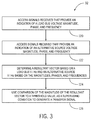
- FIG. 3 is a flow diagram illustrating an embodiment of a process and/or instructions useful in performing resultant V/Hz monitoring 92. Accordingly, the process begins by accessing signals (block 120) received that provide a LB health indication.
- the health indication may include the LB voltage magnitude value 66, LB phase value 68, and LB frequency value 70. Additionally, the process may include accessing signals (block 122) received that provide a health indication of the AS 16.
- the health indication AS voltage magnitude 76, AS phase 78, and AS frequency 80.
- the process includes determining, via the processor, a resultant vector based on a LB V/Hz and an AS V/Hz (block 124).
- the LB V/Hz vector may be based on the LB voltage magnitude value 66, the LB phase value 68, and the LB frequency value 70 (e.g., phasor voltage divided by frequency).
- the AS V/Hz may be based on the AS voltage magnitude value 76, AS phase value 78, and AS frequency value 80 (e.g., phasor voltage divided by frequency).
- the resultant vector may be a difference between the LB V/Hz vector and the AS V/Hz vector.
- the process may then continue by using a comparison of the magnitude of the resultant vector to a threshold value (e.g., 1.33 per unit), as a supervising condition to generate a transfer signal (block 126).
- the transfer signal may be configured to control a circuit breaker (e.g., PS circuit breaker 22 and/or AS circuit breaker 24). For instance, if the resultant vector exceeds the threshold value, the transfer signal may provide an indication to keep the AS circuit breaker 24 open and the PS circuit breaker 22 closed. Additionally, if the resultant vector is below the threshold value, the transfer signal may provide an indication to close the AS circuit breaker 24 and open the PS circuit breaker 22, thereby allowing the AS 16 to provide power for the loads on the LB 18.
- a threshold value e.g., 1.33 per unit
- the one or more processors may calculate supervising conditions including but not limited to a resultant vector based on a LB V/Hz vector and an AS V/Hz vector.
- the LB V/Hz vector is based on a LB voltage magnitude value 66, a LB phase angle value 68, and a LB frequency value 70.
- the AS V/Hz vector is based on an AS voltage magnitude value 76, an AS angle value 78, and an AS frequency value 80. As these transfer events occur with circuit breakers opening and closing, information may be captured about each event and used for learning and providing adjustments.
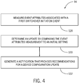
- FIG. 4 is another flow diagram illustrating an embodiment of a process and/or instructions useful in performing event attributes estimation and archiving by the HS-PST system 12.
- the process begins by accessing signals (block 128) received that provide an indication of an event attribute measurement during a first switchover event.
- Various event attributes during a transfer event may be captured and measured from the PS 14, AS 16, and LB 18. More specifically, event attributes may be tracked and measured related to the voltage magnitude decay rate of the LB 18, the spin-down rates of the LB voltage transformer 34, or circuit breaker open/close time tracking.
- one or more processors may be configured to measure event attributes associated with a first switchover initiation event.
- a signal is received from the PS 14, the AS 16, the LB 18, or any combination thereof.
- the switchover initiation event comprises switching over power delivered to the loads 20 on the LB 18 from the PS 14 to the AS 16.
- the process may continue by determining an update (block 130) by comparing the estimated last event attributes measurement to initial settings.
- the update may be related to synchronizing the LB 18 with the AS 16 during a second switchover event.
- the processors may determine the update (block 130) by comparing the event attributes measurement to initial settings.
- the update may be related to the LB 18 and the AS 16 during a second switchover event, the comparison to a magnitude, a phase, a frequency, a slip, an acceleration, or any combination thereof of the AS 16 or the LB 18, and supervising conditions.
- the event attribute measurement may correspond to a voltage magnitude decay rate of the LB 18.
- the voltage magnitude decay rate of the LB 18 may be used as an indicator to lessen loads.
- the event attribute measurement may correspond to a spin-down rate of the LB voltage phase angle 68, LB voltage frequency 70, slip 72, and acceleration 74.
- the spin-down rate may provide an indication of an opportunity period for closing the AS circuit breaker 24.
- a faster spin-down rate may indicate that critical components stop operating faster.
- the event attribute measurement may also correspond to an open time or close time of the PS circuit breaker 22 and/or the AS circuit breaker 24. As circuit breakers age, the time it takes to close/open the circuit breaker may change. This time is used above when considering synchronization of the sources and bus.
- the process continues by generating an update signal that provides an indication of the update. That is, the one or more processors may generate a notification that provides recommendations for a device configuration update (block 132). This notification may be sent to a workstation, may be used in the high speed synchronizer 26, or used in a generated report. If, for instance, the circuit breaker timing has changed, an operator may see the report or the information displayed on the workstation and update the circuit breaker. Alternatively, the high speed synchronizer 26 may use the update signal (e.g., notification) and update the synchronizer prediction 88 information.
- the update signal e.g., notification
- the event attributes include a voltage magnitude decay rate on the LB 18, a spin down of the load on the LB 18, an electrical torque, an operation time of switches available during connection of the AS 16, or any combination thereof.
- the spin down may correspond to the phase angle 68, frequency 70, slip 72, acceleration 74, or any combination thereof of the LB 18.
- the event attributes correspond to statistical value related to all event attributes. That is, the statistical value may include a minimum, an average, a maximum, or a standard deviation of event attributes.
- the LB values may be determined using any suitable method, such as dual buffer sampling interval transfer with frequency tracking or using adaptive least error square with a look up table from frequency tracking. That is, some embodiments may calculate the angle 68 of the LB 18 by applying Least Error Square with a fixed number of coefficients.
- FIG. 5 is a schematic diagram showing the dual buffer sampling interval transfer. Frequency tracking is obtained from the remaining healthy source (e.g., AS 16). More specifically, the LB signals may be estimated according to the measured LB frequency 70. The LB signals are stored in a large variable length buffer 102 for one cycle of the LB frequency 70. As shown in FIG.
- a large data buffer 102 may be used with samples based on the frequency tracking from AS 16.
- the data buffer may include a variable number of bits 104.
- the estimated data is inserted into a fixed length data buffer 106 sampled interval and associated time stamp at Ftrack 54 from AS 16..
- the variable length buffer 102 may be a larger buffer than the fixed length buffer 106.
- the variable length buffer 102 is configured to adjust the variable sampling interval and associated time stamps based on the tracking frequency.
- the fixed length buffer 106 comprises a predetermined number of samples matching the LB frequency 70 and having associated time stamps.
- the fixed length size data buffer 106 includes sampling intervals and associated time stamps at fixed number of samples per LB frequency 70.
- the new sample value and associated new time stamp is estimated by performing dual buffer sampling interval transfer.
- Technical effects of the invention include using a synchronization check that indicates when to perform a high-speed power source transfer. Additionally, the system monitors transferring based on V/Hz between a primary source and an alternative source. Likewise, the system outputs updates to a user or to the system that can improve transferring between power sources. In this manner, sources are transferred when synchronized thereby allowing critical rotating motors to maintain power and continuously rotate. Timing the transfer based on compared power attributes and supervising conditions can prevent damage to the machines connected to the load bus during a switchover.
Landscapes
- Engineering & Computer Science (AREA)
- Power Engineering (AREA)
- Business, Economics & Management (AREA)
- Emergency Management (AREA)
- Physics & Mathematics (AREA)
- General Physics & Mathematics (AREA)
- Supply And Distribution Of Alternating Current (AREA)
- Power Sources (AREA)
- Direct Current Feeding And Distribution (AREA)
Abstract
Description
- The present disclosure relates generally to power source transfer. More specifically, the present disclosure relates to a high-speed power source transfer system that helps maintain power continuity to loads.
- In many industries, it is desirable to supply power continuously to critical industrial loads. For instance, it is important in the power and process industry to continuously supply power to induction and synchronous motors on a load bus. In such cases, it is helpful to have a primary power source and an alternative power source selectively electrically coupled to the load bus. For instance, the primary power source and the alternative power source may each include a circuit breaker that can connect/disconnect the power source from the loads on the load bus. By controlling the circuit breakers, a high-speed power source transfer (HS-PST) system controls which power source (e.g., the primary power source or the alternative power source) is powering the loads on the load bus. If, for example, the primary power source loses power, the HS-PST system can quickly change to the alternative power source. However, transferring to the alternative power source without synchronizing the load bus with the alternative source may lead to problems in the industrial processes and rotary machine loads.
- Certain embodiments commensurate in scope with the originally claimed invention are summarized below. These embodiments are not intended to limit the scope of the claimed invention, but rather these embodiments are intended only to provide a brief summary of possible forms of the invention. Indeed, the invention may encompass a variety of forms that may be similar to or different from the embodiments set forth below.
- In a first embodiment, an electronic device is configured to switchover power supplied from a primary source to an alternate source to maintain continuity of power supplied to a load bus. The electronic device includes one or more processors configured to identify availability of the alternate source using source monitoring in order to measure and calculate a tracking frequency for controlling a variable sampling interval of the one or more processors. The one or more processors are configured to obtain signal samples having associated time stamps from the primary source, the alternate source, and the load bus. In an embodiment, the one or more processors store load bus signal samples and associated time stamps of the load bus into a variable length buffer. In certain embodiments, the one or more processors calculate a new time stamp for transferring to a fixed length buffer from a measured load bus signal frequency for applying a dual buffer sampling interval transfer to estimate a new sample value at the calculated new time stamp. In some embodiments, the one or more processors store the new sample value and associated new time stamp into the fixed length buffer. In an embodiment, the one or more processors determine a set of attributes from samples of the alternate source using the tracking frequency and fixed length buffer samples of a load bus supply, wherein the set of attributes comprise a magnitude, an angle, a frequency, a slip, an acceleration, or any combination thereof, and calculate supervising conditions to execute a source switchover signal when the primary source is unavailable based at least in part on comparing the set of load bus attributes to alternate source attributes at an estimated instance of switchover.
- In a second embodiment, a non-transitory computer-readable medium includes stored instructions thereon. The instructions are configured to be executed by an electronic device that is configured to switchover power supplied from a primary source to an alternate source to maintain continuity of power supplied to a load bus. The instructions are configured to identify availability of the alternate source using source monitoring in order to measure and calculate a tracking frequency for controlling a variable sampling interval of one or more processors. In some embodiments, the instructions are configured to obtain signal samples having associated time stamps from the primary source, the alternate source, and the load bus. In certain embodiments, the instructions are configured to store load bus signal samples and associated time stamps of the load bus into a variable length buffer. In an embodiment, the instructions are configured to calculate a new time stamp for transferring to a fixed length buffer from a measured load bus signal frequency for applying a dual buffer sampling interval transfer to estimate a new sample value at the calculated new time stamp. In some embodiments, the instructions are configured to store the new sample value and associated new time stamp into the fixed length buffer, determine a set of attributes from samples of the alternate source using the tracking frequency and fixed length buffer samples of a load bus supply, wherein the set of attributes comprise a magnitude, an angle, a frequency, a slip, an acceleration, or any combination thereof, and calculate supervising conditions to execute a source switchover signal when the primary source is unavailable based at least in part on comparing the set of load bus attributes to alternate source attributes at an estimated instance of switchover.
- In a third embodiment, an electronic device includes a processor, wherein the processor is configured to measure event attributes associated with a first switchover initiation event, wherein a signal is received from a primary source, an alternative source, a load bus, or any combination thereof, wherein the switchover initiation event comprises switching over power delivered to a load on a load bus from the primary source to the alternative source, determine an update by comparing the event attributes measurement to initial settings, wherein the update is related to the load bus and the alternative source during a second switchover event, wherein the comparison to a magnitude, a phase, a frequency, a slip, an acceleration, or any combination thereof of the alternative source or the load bus, and supervising conditions, and generate a notification that provides recommendations for a device configuration update.
- These and other features, aspects, and advantages of the present invention will become better understood when the following detailed description is read with reference to the accompanying drawings in which like characters represent like parts throughout the drawings, wherein:
-
FIG. 1 is a schematic diagram of a system using a high-speed power source transfer system; -
FIG. 2 is a flow diagram illustrating an embodiment of a process and/or instructions useful in performing the high-speed synchro-check of the high-speed power source transfer system ofFIG. 1 ; -
FIG. 3 is a flow diagram illustrating an embodiment of a process and/or instructions useful in performing resultant V/Hz monitoring of the high-speed power source transfer system ofFIG. 1 ; -
FIG. 4 is another flow diagram illustrating an embodiment of a process and/or instructions useful in performing event parameter estimation and archiving of the high-speed power source transfer system ofFIG. 1 ; and -
FIG. 5 is a schematic diagram showing the dual buffer sampling interval transfer, as used in the high-speed power source transfer system ofFIG. 1 . - One or more specific embodiments of the present invention will be described below. In an effort to provide a concise description of these embodiments, all features of an actual implementation may not be described in the specification. It should be appreciated that in the development of any such actual implementation, as in any engineering or design project, numerous implementation-specific decisions must be made to achieve the developers' specific goals, such as compliance with system-related and business-related constraints, which may vary from one implementation to another. Moreover, it should be appreciated that such a development effort might be complex and time consuming, but would nevertheless be a routine undertaking of design, fabrication, and manufacture for those of ordinary skill having the benefit of this disclosure.
- When introducing elements of various embodiments of the present invention, the articles "a," "an," "the," and "said" are intended to mean that there are one or more of the elements. The terms "comprising," "including," and "having" are intended to be inclusive and mean that there may be additional elements other than the listed elements.
- When transferring from the primary power source to the alternative power source, synchronization and timing between the primary source, load bus, and alternative source are important to not interrupt the industrial rotating machine loads. For instance, a motor on the load bus may have a load connected to a shaft that rotates based on power attributes of the primary power source (e.g., voltage, phase, frequency). As the shaft rotates, the shaft builds/keeps inertia. When the primary power source fails, the power attributes of the primary power source and/or the load bus may not be synchronized with the alternative source (e.g., the primary source and alternative source may operate independently from each other). For instance, the load bus may lead the alternative source in phase by twenty degrees. It may be desirable for the HS-PST to change to the alternative power source after the load bus phase more closely aligns with the phase of the alternative power source (e.g., within 5 degrees of each other). As such, it is desirable to address transferring between sources in such a way that the processes (e.g., motors) on the load bus are uninterrupted.
- Turning to the figures,
FIG. 1 is a schematic diagram of asystem 10 using a high-speed power source transfer (HS-PST)system 12. Thesystem 10 includes a primary source (PS) 14 and an alternative source 16 (AS) selectively electrically coupled to loads on a load bus 18 (LB), such as, for instance, induction and/orsynchronous motors 20. ThePS 14 includes aPS circuit breaker 22, and theAS 16 includes anAS circuit breaker 24. - Under typical operating conditions, the
PS circuit breaker 22 is closed, thereby enabling thePS 14 to supply power to the loads on theLB 18. Under these conditions, the AScircuit breaker 24 is open. If thePS 14 fails, it may be desirable to transfer power sources from thePS 14 to theAS 16 by closing the AScircuit breaker 24 and opening thePS circuit breaker 22, thereby powering the loads on theLB 18 with theAS 16. That is, the HS-PST system 12 may be configured to switchover power supplied from thePS 14 to the AS 16 to maintain continuity of power supplied to theLB 18. - In order to transfer sources, the HS-
PST 12 may be used to communicate open and/or close signals with thePS circuit breaker 22 and theAS circuit breaker 24. Accordingly, ahigh speed synchronizer 26 of the HS-PST system 12 may providecontrol execution 28 configured to communicate open and/or close signals with thePS circuit breaker 22 and the AScircuit breaker 24 via contact I/O modules 30 of thehigh speed synchronizer 26. - To determine whether to open/close the circuit breakers, the HS-
PST system 12 may process signals received from thePS 14,AS 16, andLB 18. For instance, a PS voltage transformer 32, aLB voltage transformer 34, and anAS voltage transformer 36 may provide galvanic isolation (e.g., used to isolate where two or more circuits need to communicate with a device, such as the HS-PST system 12, and the circuits may be at different grounds) and enable the HS-PST system 12 to receive signals related to the health of the sources and bus. - More specifically, the HS-
PST 12 may include aPS signal processor 38, aLB signal processor 40, and an ASsignal processor 42. ThePS signal processor 38,LB signal processor 40, and the ASsignal processor 42 may process signals received from thePS 14, theLB 18, and theAS 16 respectively. As discussed below, each processing sub-system may receive signals relating to the health of the sources and bus. Thehigh speed synchronizer 26, thePS signal processor 38, theLB signal processor 40, and the ASsignal processor 42 each may include a processor or multiple processors, memory, and inputs/outputs. While the systems are depicted as separate systems, alternatively, sub-systems may share a processor or multiple processors and/or memory. The processor(s) may be operatively coupled to the memory to execute instructions for carrying out the presently disclosed techniques. These instructions may be encoded in programs and stored in a tangible non-transitory computer-readable medium, such as the memory and/or other storage. The processor may be a general purpose processor, system-on-chip (SoC) device, or application specific integrated circuit, or some other processor configuration. - Memory, in the embodiment, includes a computer readable medium, such as, without limitation, a hard disk drive, a solid state drive, a diskette, a flash drive, a compact disc, a digital video disc, random access memory (RAM), and/or any suitable storage device that enables the processor(s) to store, retrieve, and/or execute instructions and/or data. Memory may include one or more local and/or remote storage devices.
- While
FIG. 1 shows the contact I/O modules 30 as a part of the high-speed powersource transfer system 12, the contact I/O modules 30 may be separate from the HS-PST system 12. As such, the contact I/O modules 30 may communicate with any suitable wired or wireless communication protocol. For instance, the I/O modules 30 may connect to a network using, for example, a wired Ethernet protocol or a wireless Ethernet protocol. - The
high speed synchronizer 26 may communicate with aworkstation 43 using any suitable protocol (e.g., wireless or wired protocol). Theworkstation 43 may allow an operator to configure the high speed synchronizer to the specific set up where the high speed synchronizer is being used. For instance, theworkstation 43 may allow the user to specify details about themotors 20 on theLB 18, details about the circuit breakers (e.g., open/close time), details about threshold values used to detect when transfer should take place, or the like. Further, thehigh speed synchronizer 26 may communicate updates or potential changes to the instructions stored on thehigh speed synchronizer 26. - The
PS signal processor 38 may receive input signals that provide an indication ofprimary source 14 power attribute values. The input signals may be conditioned 44 (e.g., filtered, amplified, isolated, etc.), converted to digital values using sample-hold and analog-to-digital conversion 46 (S/H & ADC) techniques, processed using, for example, digital signal processing 48 (DSP), and/or estimated usingsignal parameter estimation 50. ThePS signal processor 38 may determine power attribute values, such as a PSvoltage magnitude value 56, PS phase value 58,PS frequency value 60,PS slip value 62, and PS acceleration value 64 (e.g., rate of change of the primary source slip value 62). Once the PSvoltage magnitude value 56, PS phase value 58,PS frequency value 60,PS slip value 62, andPS acceleration value 64 are determined, thePS signal processor 38 may transmit an indication of the primary source power attribute values to thehigh speed synchronizer 26. - Similarly, the
LB signal processor 40 may receive input signals that provide an indication of theLB 18 power attribute values. The input signals received by theLB signal processor 40 may be conditioned 44 (e.g., filtered, amplified, isolated, etc.), converted to digital values using sample-hold and analog-to-digital conversion 46 (S/H & ADC) techniques, processed using, for example, digital signal processing 48 (DSP), and/or estimated usingsignal parameter estimation 50. TheLB signal processor 40 may determine power attribute values, such as a LB voltage magnitude value 66, LB voltage phase value 68,LB frequency value 70,LB slip value 72, and a LB acceleration value 74 (e.g., rate of change of the LB slip value 72). Additionally, theLB signal processor 40 may receive the frequency from the remaining healthy bus. As further described below, theLB signal processor 40 may perform dual buffersampling interval transfer 52 by tracking the AS frequency. Once the power attribute values are determined, the values may be sent to thehigh speed synchronizer 26. In an embodiment, the magnitude of LB signals use a Root-Mean-Square (RMS) value, and the magnitude of the primary and auxiliary supply uses non-recursive full cycle Discrete Fourier Transform (DFT). In some embodiments, one or more processors of the HS-PST system 12 may be configured to calculate the angle (e.g., LB phase value 68) of theLB 18 by utilizing a rotationary recursive Discrete Fourier Transform - Likewise, the
AS signal processor 42 may receive input signals that provide an indication of AS power attribute values. The input signals received by theAS signal processor 42 may be conditioned 44 (e.g., filtered, amplified, isolated, etc.), converted to digital values using sample-hold and analog-to-digital conversion 46 (S/H & ADC) techniques, processed using, for example, digital signal processing 48 (DSP), and/or estimated usingsignal parameter estimation 50. TheAS signal processor 42 may determine power attribute values, such as an ASvoltage magnitude value 76, AS phase value 78, ASfrequency value 80, ASslip value 82, and an AS acceleration value 84 (e.g., rate of change of the AS slip value 82). Once the power attribute values are determined, the values may be sent to thehigh speed synchronizer 26. To determine one or more of the slip values 62, 72, 82, one or more processors may be configured to calculate a first derivative of the measuredfrequency acceleration frequency acceleration - Because the
LB 18 is connected to a source that is failing, additional processes may be used to find the LB voltage magnitude value 66, LB phase value 68,LB frequency value 70,LB slip value 72, andLB acceleration value 74. As mentioned above, theAS signal processor 42 may transmit an indication of the AS frequency tracking value to theLB signal processor 40 and/or thePS signal processor 38. Frequency tracking (Ftrack) 54 may be obtained from the remaining healthy source (e.g., the AS 16). Frequency tracking is used to resample the LB data at the rate of, for example, theAS frequency 80. As further explained below, frequency tracking 54 on the remaining healthy source may enable measurement of the LB voltage magnitude value 66, LB voltage phase value 68,LB frequency value 70,LB slip value 72, andLB acceleration value 74. - After transitioning to the
AS 16, theAS 16 may power theLB 18. When power is restored on thePS 14, the system may transfer back to thePS 14 or continue to receive power from theAS 16. If power is not transferred, eventually theAS 16 may fail and it is desirable to transfer to thePS 14. If theAS 16 is the failing source (e.g., theAS circuit breaker 24 is closed), thePS signal processor 38 may obtain the Ftrack using the PS 14 (e.g., the healthy source). In a further embodiment, adaptive least error square may be used with a look up table of coefficients to calculate LB voltage phase properly. As such, any suitable method may be used to determine the LB power attribute values. - As mentioned above, the high-
speed synchronizer 26 may include a processor or processors operatively coupled to memory that enables the processor to store, retrieve, and/or execute instructions and/or data. As such, the high-speed synchronizer may include a tangible non-transitory computer-readable medium having stored instructions thereon. Accordingly, the high-speed synchronizer may include instructions (e.g., software) and/or hardware to performcontrol execution 28, continuous source monitoring 86,synchronizer predictions 88, high-speed synchrochecks 90, resultant V/Hz monitoring 92, and event parameter estimation &archiving 94. Continuous source monitoring 86 may include monitoring thePS 14, AS 16, andLB 18 for any signs of failures. In an embodiment, the source monitoring 86 comprises continuously monitoring voltage magnitude, frequency, and power quality of theAS 16 within a specified range. One or more of the processors may be configured to identify availability of theAS 16 using source monitoring 86 in order to measure and calculate a tracking frequency (e.g., Ftrack 54) for controlling a variable sampling interval of the one or more processors. Further, the one or more processors may obtain signal samples having associated time stamps from thePS 14, theAS 16, and theLB 18, and/or store LB signal samples and associated time stamps of the LB into a variable length buffer (shown inFIG. 5 as buffer 104). The one or more processor may then store the new sample value and associated new time stamp into the fixed length buffer (shown inFIG. 5 as buffer 108). Further, the one or more processors may determine a set of power attributes from samples of theAS 16 using the tracking frequency (e.g., Ftrack 54) and fixed length buffer samples of a LB supply, wherein the set of power attributes comprises a magnitude(e.g.,voltage magnitude value 56, 66, 76), an angle (e.g., phase values 58, 68, 78), a frequency (e.g., frequency values 60, 70, 80), a slip (e.g., slip values 62, 72, 82), an acceleration (e.g., acceleration values 64, 74, 84), or any combination thereof. Then, the one or more processors may calculate supervising conditions to execute a source switchover signal when thePS 14 is unavailable based at least in part on comparing the set of LB power attributes to AS power attributes at an estimated instance of switchover. -
Synchronizer prediction 88 may include predicting an open/close time of thePS circuit breaker 22 and/or theAS circuit breaker 24. The high-speed synchro-check 90 may include determining whether power attributes of the AS source and the load bus are synchronized. The resultant V/Hz monitoring 92 may further compare theAS 16 to theLB 18 to prevent any potential damage to machines connected to theLB 18 due to transferring sources. The event parameter estimation &archiving 94 may include revising settings or adapting the HS-PST 12. Event parameter estimation &archiving 94 may involve communication with a data storage 98. The data storage 98 may include memory, a database, or other storage device. -
FIG. 2 is a flow diagram illustrating an embodiment of aprocess 110 and/or instructions useful in performing high speed power source transfer. Theprocess 110 may begin by monitoring theAS 16 and calculating tracking frequency (e.g., Ftrack 54) to control variable sampling intervals of one or more processors (block 112). The one or more processors may continue by obtaining signal samples with associated time stamps from the primary source, the alternative source, and the load bus (block 114). The one or more processors (e.g., the LB signal processor 40) may then include storing load bus signal samples and associated time stamps (e.g., in the memory) and performing a dual buffer sampling interval transfer 52 (block 116). Next, the one or more processors may determine and compare a set of power attributes from theAS 16 and theLB 18 supply (block 118). Further, theprocess 110 may include calculating supervising conditions to execute a source switchover at an estimated instance (block 119). - The high-speed synchro-
check 90 may be used to determine whether the signals along theAS 16, andLB 18 are synchronized. More specifically, a processor of the HS-PST 10 (e.g., a processor of the high speed synchronizer module) may be configured to access signals received that provide an indication of the LB power attribute. The LB power attribute may be the LB voltage magnitude 66, phase 68,frequency 70,slip 72, acceleration, or any combination thereof. Further, the processor may be configured to access signals received that provide an indication of an AS power attribute. Similarly, the AS power attribute may be theAS voltage magnitude 76, phase 78,frequency 80,slip 82,acceleration 84, or any combination thereof. The signals may be received while a first circuit breaker (e.g., PS circuit breaker 22) is closed and a second circuit breaker (e.g., AS circuit breaker 24) is open. - The processor performing the high-speed synchro-
check 90 may also determine a transfer time based at least in part on the LB power attribute and the AS power attribute. For instance, the transfer time may be based on a comparison or difference between the LB phase 68 and the AS phase 78. The transfer time may provide an indication of a time to perform a transfer from thePS 14 to theAS 16. In addition, other signals may be used to determine the transfer time, such as the LB voltage magnitude value 66,LB frequency value 70,LB slip value 72,LB acceleration value 74, ASvoltage magnitude value 76, ASfrequency value 80, ASslip value 82, ASacceleration value 84, or any combination thereof. Additionally,synchronizer predictions 88 may be used in determining the transfer time. More specifically, the transfer time may be based at least in part on the time it takes for the first circuit breaker to open and/or the time it takes for the second circuit breaker to close. For instance, both circuit breakers take a total of 100 milliseconds to open/close after receiving the signals from the contact I/O module 30. As such, the transfer time may be based on if the LB phase angle value 68 and the AS phase angle value 78 would fall within a preset range after 100 milliseconds (e.g., after the first circuit breaker opens and the second circuit breaker closes). The preset range may be user programmable or hard coded. As discussed below, the LB signals may be based on frequency tracking using the AS signals. Alternatively, the LB signals may be based on a look up table of coefficients configured for Least Error Square (LES) processing to calculate the LB phase value 68. Then, the processor may generate a circuit breaker signal based on the transfer time. The circuit breaker signal may be configured to open the first circuit breaker and/or close the second circuit breaker to perform the transfer. - The high-speed syncho-checks performs comparisons between voltages, phases, frequencies, slips, and accelerations of the
LB 18 and theAS 16. These checks are performed to transfer power when the sources are synchronized in part to ensure that machines are not damaged. Resultant V/Hz monitoring 92 is an additional process of ensuring that settings are desirable for switchover. It involves comparing a combination of the voltage magnitude and phase (e.g., phasor) and the frequency. This may be an important consideration when any one comparison is within the preset range (e.g., the LB voltage magnitude and AS voltage magnitude are within the preset range), but the combination falls outside of the range. -
FIG. 3 is a flow diagram illustrating an embodiment of a process and/or instructions useful in performing resultant V/Hz monitoring 92. Accordingly, the process begins by accessing signals (block 120) received that provide a LB health indication. The health indication may include the LB voltage magnitude value 66, LB phase value 68, andLB frequency value 70. Additionally, the process may include accessing signals (block 122) received that provide a health indication of theAS 16. The health indication ASvoltage magnitude 76, AS phase 78, and ASfrequency 80. - The process includes determining, via the processor, a resultant vector based on a LB V/Hz and an AS V/Hz (block 124). The LB V/Hz vector may be based on the LB voltage magnitude value 66, the LB phase value 68, and the LB frequency value 70 (e.g., phasor voltage divided by frequency). Similarly, the AS V/Hz may be based on the AS
voltage magnitude value 76, AS phase value 78, and AS frequency value 80 (e.g., phasor voltage divided by frequency). The resultant vector may be a difference between the LB V/Hz vector and the AS V/Hz vector. The process may then continue by using a comparison of the magnitude of the resultant vector to a threshold value (e.g., 1.33 per unit), as a supervising condition to generate a transfer signal (block 126).. The transfer signal may be configured to control a circuit breaker (e.g.,PS circuit breaker 22 and/or AS circuit breaker 24). For instance, if the resultant vector exceeds the threshold value, the transfer signal may provide an indication to keep theAS circuit breaker 24 open and thePS circuit breaker 22 closed. Additionally, if the resultant vector is below the threshold value, the transfer signal may provide an indication to close theAS circuit breaker 24 and open thePS circuit breaker 22, thereby allowing theAS 16 to provide power for the loads on theLB 18. As such, in some embodiments, the one or more processors may calculate supervising conditions including but not limited to a resultant vector based on a LB V/Hz vector and an AS V/Hz vector. The LB V/Hz vector is based on a LB voltage magnitude value 66, a LB phase angle value 68, and aLB frequency value 70. The AS V/Hz vector is based on an ASvoltage magnitude value 76, an AS angle value 78, and an ASfrequency value 80. As these transfer events occur with circuit breakers opening and closing, information may be captured about each event and used for learning and providing adjustments. -
FIG. 4 is another flow diagram illustrating an embodiment of a process and/or instructions useful in performing event attributes estimation and archiving by the HS-PST system 12. The process begins by accessing signals (block 128) received that provide an indication of an event attribute measurement during a first switchover event. Various event attributes during a transfer event may be captured and measured from thePS 14, AS 16, andLB 18. More specifically, event attributes may be tracked and measured related to the voltage magnitude decay rate of theLB 18, the spin-down rates of theLB voltage transformer 34, or circuit breaker open/close time tracking. For instance, one or more processors may be configured to measure event attributes associated with a first switchover initiation event. In some embodiments, a signal is received from thePS 14, theAS 16, theLB 18, or any combination thereof. The switchover initiation event comprises switching over power delivered to theloads 20 on theLB 18 from thePS 14 to theAS 16. - Once the signals are received, the process may continue by determining an update (block 130) by comparing the estimated last event attributes measurement to initial settings. The update may be related to synchronizing the
LB 18 with theAS 16 during a second switchover event. For instance, the processors may determine the update (block 130) by comparing the event attributes measurement to initial settings. The update may be related to theLB 18 and theAS 16 during a second switchover event, the comparison to a magnitude, a phase, a frequency, a slip, an acceleration, or any combination thereof of theAS 16 or theLB 18, and supervising conditions. - The event attribute measurement may correspond to a voltage magnitude decay rate of the
LB 18. The voltage magnitude decay rate of theLB 18 may be used as an indicator to lessen loads. Additionally and/or alternatively, the event attribute measurement may correspond to a spin-down rate of the LB voltage phase angle 68,LB voltage frequency 70,slip 72, andacceleration 74. The spin-down rate may provide an indication of an opportunity period for closing theAS circuit breaker 24. A faster spin-down rate may indicate that critical components stop operating faster. As mentioned above, the event attribute measurement may also correspond to an open time or close time of thePS circuit breaker 22 and/or theAS circuit breaker 24. As circuit breakers age, the time it takes to close/open the circuit breaker may change. This time is used above when considering synchronization of the sources and bus. As such, it may be beneficial to track CB times. This may be determined based on a difference between the entered circuit breaker operation time and the actual measured circuit breaker operation time (e.g., command initiation time to actual circuit breaker contact open/close time). Once the update is determined, the process continues by generating an update signal that provides an indication of the update. That is, the one or more processors may generate a notification that provides recommendations for a device configuration update (block 132). This notification may be sent to a workstation, may be used in thehigh speed synchronizer 26, or used in a generated report. If, for instance, the circuit breaker timing has changed, an operator may see the report or the information displayed on the workstation and update the circuit breaker. Alternatively, thehigh speed synchronizer 26 may use the update signal (e.g., notification) and update thesynchronizer prediction 88 information. - In some embodiments, the event attributes include a voltage magnitude decay rate on the
LB 18, a spin down of the load on theLB 18, an electrical torque, an operation time of switches available during connection of theAS 16, or any combination thereof. For instance, the spin down may correspond to the phase angle 68,frequency 70,slip 72,acceleration 74, or any combination thereof of theLB 18. In certain embodiments, the event attributes correspond to statistical value related to all event attributes. That is, the statistical value may include a minimum, an average, a maximum, or a standard deviation of event attributes. - As the
LB frequency 70 decays, the number of samples performed in one cycle of the LB increases. As mentioned above, the LB values may be determined using any suitable method, such as dual buffer sampling interval transfer with frequency tracking or using adaptive least error square with a look up table from frequency tracking. That is, some embodiments may calculate the angle 68 of theLB 18 by applying Least Error Square with a fixed number of coefficients.FIG. 5 is a schematic diagram showing the dual buffer sampling interval transfer. Frequency tracking is obtained from the remaining healthy source (e.g., AS 16). More specifically, the LB signals may be estimated according to the measuredLB frequency 70. The LB signals are stored in a largevariable length buffer 102 for one cycle of theLB frequency 70. As shown inFIG. 5 , alarge data buffer 102 may be used with samples based on the frequency tracking from AS 16. The data buffer may include a variable number ofbits 104. The estimated data is inserted into a fixedlength data buffer 106 sampled interval and associated time stamp atFtrack 54 from AS 16.. Further, in some embodiments, thevariable length buffer 102 may be a larger buffer than the fixedlength buffer 106. Thevariable length buffer 102 is configured to adjust the variable sampling interval and associated time stamps based on the tracking frequency. Additionally, the fixedlength buffer 106 comprises a predetermined number of samples matching theLB frequency 70 and having associated time stamps. The fixed lengthsize data buffer 106 includes sampling intervals and associated time stamps at fixed number of samples perLB frequency 70. In an embodiment, the new sample value and associated new time stamp is estimated by performing dual buffer sampling interval transfer. - Technical effects of the invention include using a synchronization check that indicates when to perform a high-speed power source transfer. Additionally, the system monitors transferring based on V/Hz between a primary source and an alternative source. Likewise, the system outputs updates to a user or to the system that can improve transferring between power sources. In this manner, sources are transferred when synchronized thereby allowing critical rotating motors to maintain power and continuously rotate. Timing the transfer based on compared power attributes and supervising conditions can prevent damage to the machines connected to the load bus during a switchover.
- This written description uses examples to disclose the invention, including the best mode, and also to enable any person skilled in the art to practice the invention, including making and using any devices or systems and performing any incorporated methods. The patentable scope of the invention is defined by the claims, and may include other examples that occur to those skilled in the art. Such other examples are intended to be within the scope of the claims if they have structural elements that do not differ from the literal language of the claims, or if they include equivalent structural elements with insubstantial differences from the literal language of the claims.
- Various aspects and embodiments of the present invention are defined by the following numbered clauses:
- 1. An electronic device, comprising:
- a processor, wherein the processor is configured to:
- measure event attributes associated with a first switchover initiation event, wherein a signal is received from a primary source, an alternative source, a load bus, or any combination thereof, wherein the switchover initiation event comprises switching over power delivered to a load on a load bus from the primary source to the alternative source;
- determine an update by comparing the event attributes measurement to initial settings, wherein the update is related to the load bus and the alternative source during a second switchover event, wherein the comparison to a magnitude, a phase, a frequency, a slip, an acceleration, or any combination thereof of the alternative source or the load bus, and supervising conditions; and
- generate a notification that provides recommendations for a device configuration update.
- a processor, wherein the processor is configured to:
- 2. The electronic device of clause 1, wherein the event attributes comprise a voltage magnitude decay rate on the load bus, a spin down of the load on the load bus, an electrical torque, an operation time of switches available during connection of the alternate supply, or any combination thereof.
- 3. The electronic device of clause 1 or 2, wherein the spin down corresponds to the phase angle, frequency, slip, acceleration, or any combination thereof of the load bus.
- 4. The electronic device of any preceding clause, wherein the event attributes correspond to statistical value related to all event attributes.
- 5. The electronic device of any preceding clause, comprising a minimum, an average, a maximum, or a standard deviation of event attributes as the statistical value.
Claims (16)
- An electronic device configured to switchover power supplied from a primary source (14) to an alternate source (16) to maintain continuity of power supplied to a load bus (18), wherein the electronic device comprises one or more processors (38,40,42) configured to:identify availability of the alternate source using source monitoring in order to measure and calculate a tracking frequency for controlling a variable sampling interval of the one or more processors (38,40,42);obtain signal samples having associated time stamps from the primary source (14), the alternate source (16), and the load bus (18);store load bus signal samples and associated time stamps of the load bus (18) into a variable length buffer (104);calculate a new time stamp for transferring to a fixed length buffer (108) from a measured load bus signal frequency for applying a dual buffer sampling interval transfer (52) to estimate a new sample value at the calculated new time stamp;store the new sample value and associated new time stamp into the fixed length buffer;determine a set of attributes from samples of the alternate source (16) using the tracking frequency and fixed length buffer samples of a load bus supply, wherein the set of attributes comprise a magnitude (56), an angle (58), a frequency (60), a slip (62), an acceleration (64), or any combination thereof; andcalculate supervising conditions to execute a source switchover signal when the primary source (14) is unavailable based at least in part on comparing the set of load bus (18) attributes to alternate source (16) attributes at an estimated instance of switchover.
- The electronic device of claim 1, wherein the source monitoring comprises continuously monitoring voltage magnitude (70), frequency (78), and power quality (80) of the alternate source (16) within a specified range.
- The electronic device of claim 1 or 2, wherein the variable length buffer (104) is a larger buffer than the fixed length buffer (106), and wherein the variable length buffer (104) is configured to adjust the variable sampling interval and associated time stamps based on the tracking frequency, wherein the fixed length buffer (106) comprises a predetermined number of samples matching load bus frequency and having associated time stamps.
- The electronic device of any of claims 1 to 3, wherein the new sample value and associated new time stamp is estimated by performing dual buffer sampling interval transfer (52).
- The electronic device of any of claims 1 to 4, wherein the magnitude of load bus signals uses a Root-Mean-Square (RMS) value, and the magnitude of the primary and auxiliary supply uses non-recursive full cycle Discrete Fourier Transform (DFT).
- The electronic device of any preceding claim, wherein the one or more processors (38,40,42) are configured to calculate the angle of the load bus (18) by utilizing a rotationary recursive Discrete Fourier Transform.
- The electronic device of any preceding claim, wherein the one or more processors (38,40,42) are configured to calculate a first derivative and a second derivative of the measured frequency as the slip and the acceleration, respectively.
- The electronic device of any preceding claim, wherein the one or more processors (38,40,42) are configured to calculate supervising conditions including but not limited to a resultant vector based on a load bus volts per hertz vector and an alternate source volts per hertz vector, wherein the load bus volts per hertz vector is based on a load bus voltage magnitude value (66), a load bus phase angle value (68), and a load bus frequency value (70), and wherein the alternate source (16) volts per hertz vector is based on an alternate source voltage magnitude value (76), an alternate source angle value (78), and an alternate source frequency value (80).
- A method for switchover of the power supplied from a primary source (14) to an alternate source (16) to maintain continuity of power supplied to a load bus (18), the method comprising:identifying availability of the alternate source (16) using source monitoring in order to measure and calculate a tracking frequency for controlling a variable sampling interval of one or more processors (38,40,42);obtaining signal samples having associated time stamps from the primary source (14), the alternate source (16), and the load bus (18);storing load bus signal samples and associated time stamps of the load bus (18) into a variable length buffer (104);calculating a new time stamp for transferring to a fixed length buffer (106) from a measured load bus signal frequency for applying a dual buffer sampling interval transfer (52) to estimate a new sample value at the calculated new time stamp;storing the new sample value and associated new time stamp into the fixed length buffer (106);determining a set of attributes from samples of the alternate source using the tracking frequency and fixed length buffer samples of a load bus supply, wherein the set of attributes comprise a magnitude, an angle, a frequency, a slip, an acceleration, or any combination thereof; andcalculating supervising conditions to execute a source switchover signal when the primary source (14) is unavailable based at least in part on comparing the set of load bus attributes to alternate source attributes at an estimated instance of switchover.
- The method of claim 9, further comprising calculating supervising conditions including but not limited to a resultant vector based on a load bus volts per hertz vector and an alternate source volts per hertz vector, wherein the load bus volts per hertz vector is based on a load bus voltage magnitude value (60), a load bus phase angle value (68), and a load bus frequency value (70), and wherein the alternate source volts per hertz vector is based on an alternate source voltage magnitude value (76), an alternate source angle value (78), and an alternate source frequency value (80).
- The method of claim 9 or 10, further comprising calculating a first derivative and a second derivative of the measured frequency as the slip and the acceleration, respectively.
- The method of any of claims 9 to 11, wherein the magnitude of load bus signals uses a Root-Mean-Square (RMS) value, and the magnitude of the primary and auxiliary supply uses non-recursive full cycle Discrete Fourier Transform (DFT).
- The method of any of claims 9 to 12, wherein the variable length buffer (104) is a larger buffer than the fixed length buffer (108), and wherein the variable length buffer (104) is configured to adjust the variable sampling interval and associated time stamps based on the tracking frequency, wherein the fixed length buffer (106) comprises a predetermined number of samples matching load bus frequency and having associated time stamps.
- The method of any of claims 9 to 13, further comprising calculating the angle of the load bus (18) by utilizing a rotationary recursive Discrete Fourier Transform or calculating the angle of the load bus (18) by applying Least Error Square with a fixed number of coefficients.
- A computer program comprising computer code means adapted to perform the method of any of claims 9 to 14, when executed by a computer.
- The computer program of claim 15, embodied on a computer-readable medium.
Applications Claiming Priority (1)
| Application Number | Priority Date | Filing Date | Title |
|---|---|---|---|
| US14/673,316 US9800088B2 (en) | 2015-03-30 | 2015-03-30 | Method and system for high-speed power source transfer (HS-PST) |
Publications (2)
| Publication Number | Publication Date |
|---|---|
| EP3076514A1 true EP3076514A1 (en) | 2016-10-05 |
| EP3076514B1 EP3076514B1 (en) | 2020-07-22 |
Family
ID=55910088
Family Applications (1)
| Application Number | Title | Priority Date | Filing Date |
|---|---|---|---|
| EP16161975.4A Not-in-force EP3076514B1 (en) | 2015-03-30 | 2016-03-23 | A method and system for high-speed power source transfer (hs-pst) |
Country Status (6)
| Country | Link |
|---|---|
| US (1) | US9800088B2 (en) |
| EP (1) | EP3076514B1 (en) |
| JP (1) | JP2016192890A (en) |
| CN (1) | CN106026352A (en) |
| BR (1) | BR102016006731A2 (en) |
| CA (1) | CA2923938C (en) |
Families Citing this family (2)
| Publication number | Priority date | Publication date | Assignee | Title |
|---|---|---|---|---|
| US11018497B2 (en) | 2019-04-09 | 2021-05-25 | Schweitzer Engineering Laboratories, Inc. | In-phase motor bus transfer |
| US11736051B2 (en) | 2021-08-05 | 2023-08-22 | Schweitzer Engineering Laboratories, Inc. | Synchronous motor startup configuration to synchronous mode at a field zero-crossing |
Citations (1)
| Publication number | Priority date | Publication date | Assignee | Title |
|---|---|---|---|---|
| US20080111507A1 (en) * | 2006-11-14 | 2008-05-15 | Yalla Murty V V S | Digital system for motor bus transfer |
Family Cites Families (16)
| Publication number | Priority date | Publication date | Assignee | Title |
|---|---|---|---|---|
| JPS57113632U (en) * | 1981-01-05 | 1982-07-14 | ||
| JPH0471132A (en) * | 1990-07-10 | 1992-03-05 | Toshiba Corp | Ac circuit breaker and control method thereof |
| EP0604540B1 (en) | 1991-09-20 | 1996-01-10 | Siemens Aktiengesellschaft | Measuring process for obtaining a switching command in a rapid changeover device |
| JPH06153551A (en) * | 1992-10-29 | 1994-05-31 | Toshiba Corp | AC motor starter |
| JPH06284584A (en) * | 1993-03-26 | 1994-10-07 | Fuji Electric Co Ltd | Automatic synchronizer |
| US5761073A (en) | 1995-02-09 | 1998-06-02 | Basler Electric Company | Programmable apparatus for synchronizing frequency and phase of two voltage sources |
| JPH10341531A (en) * | 1997-06-06 | 1998-12-22 | Toshiba Corp | Overload monitoring system for transformer |
| JP2001258145A (en) * | 2000-03-10 | 2001-09-21 | Toshiba Corp | Protection relay system |
| JP2003061248A (en) * | 2001-08-10 | 2003-02-28 | Mitsubishi Electric Corp | Power system switching device |
| US7589438B2 (en) | 2004-07-09 | 2009-09-15 | Layerzero Power Systems, Inc. | Source phase sensitive transfer method and apparatus |
| JP2007097316A (en) * | 2005-09-29 | 2007-04-12 | Mitsubishi Electric Corp | Bus switching device |
| US8373309B2 (en) | 2009-08-19 | 2013-02-12 | Schweitzer Engineering Laboratories Inc | Systems and methods for asynchronous sampling data conversion |
| US10240593B2 (en) * | 2011-03-04 | 2019-03-26 | Asco Power Technologies, L.P. | Systems and methods of controlling pressure maintenance pumps and data logging pump operations |
| EP2595265A1 (en) * | 2011-11-17 | 2013-05-22 | Siemens Aktiengesellschaft | Power supply system of a marine vessel |
| US9054586B2 (en) * | 2013-03-15 | 2015-06-09 | Rockwell Automation Technologies, Inc. | Methods and apparatus for continuous and discontinuous active rectifier boost operation to increase power converter rating |
| CN104142422A (en) * | 2013-05-08 | 2014-11-12 | 伍俊 | Transformation substation leakage current and capacitive current online monitoring management system and working method thereof |
-
2015
- 2015-03-30 US US14/673,316 patent/US9800088B2/en active Active
-
2016
- 2016-03-17 CA CA2923938A patent/CA2923938C/en active Active
- 2016-03-23 JP JP2016057763A patent/JP2016192890A/en active Pending
- 2016-03-23 EP EP16161975.4A patent/EP3076514B1/en not_active Not-in-force
- 2016-03-28 BR BR102016006731A patent/BR102016006731A2/en not_active IP Right Cessation
- 2016-03-30 CN CN201610189991.1A patent/CN106026352A/en active Pending
Patent Citations (1)
| Publication number | Priority date | Publication date | Assignee | Title |
|---|---|---|---|---|
| US20080111507A1 (en) * | 2006-11-14 | 2008-05-15 | Yalla Murty V V S | Digital system for motor bus transfer |
Also Published As
| Publication number | Publication date |
|---|---|
| CA2923938A1 (en) | 2016-09-30 |
| JP2016192890A (en) | 2016-11-10 |
| CN106026352A (en) | 2016-10-12 |
| US9800088B2 (en) | 2017-10-24 |
| CA2923938C (en) | 2023-08-01 |
| BR102016006731A2 (en) | 2016-10-04 |
| US20160294212A1 (en) | 2016-10-06 |
| EP3076514B1 (en) | 2020-07-22 |
Similar Documents
| Publication | Publication Date | Title |
|---|---|---|
| Liu et al. | Recent developments of FNET/GridEye—A situational awareness tool for smart grid | |
| US7698582B2 (en) | Apparatus and method for compensating digital input delays in an intelligent electronic device | |
| CN101363896B (en) | A high-precision voltage transient event detection and wave recording method | |
| US11616370B2 (en) | Recloser control with distributed energy resource synchronization | |
| EP3076514B1 (en) | A method and system for high-speed power source transfer (hs-pst) | |
| WO2008148428A1 (en) | Method and device to predict a state of a power system in the time domain | |
| US11005584B2 (en) | Clock synchronization in a device | |
| CN108292859A (en) | Uninterrupted power supply | |
| US10110057B2 (en) | Transfer switch apparatus and methods using transition time monitoring and adaptation | |
| WO2015038424A1 (en) | Detection of faults in power distribution system | |
| CN104991628B (en) | Data center intelligent power monitoring system and monitoring method | |
| US20180372782A1 (en) | Systems and methods for monitoring power | |
| WO2012138340A1 (en) | Systems and methods for determining a power phase and/or a phase rotation | |
| JP2010104158A (en) | Uninterruptible power supply unit and method for selectively interrupting uninterruptible power supply unit | |
| US20140281649A1 (en) | Method For Automatic Mapping Of AC Phase Conductors And Identification Of AC Buses In A Multi-Bus Power System | |
| US9673994B2 (en) | Synchrophasor data management systems and methods | |
| CN110350516B (en) | Automatic identification method for single-ring network topology of high-voltage distribution network | |
| KR100981786B1 (en) | Variable analog interface module and wide area power system dynamic monitoring system having the same | |
| CN104331060B (en) | A kind of phase-controlled device option principle method for testing precision of breaker | |
| JP2009296829A (en) | Uninterruptible power supply system | |
| US20200389027A1 (en) | Microgrid Autosynchronizing Using Remote Recloser Inputs and Outputs | |
| RU2589400C2 (en) | Automated system recording, collection, processing, storage and viewing by emergency power system operator of oscillographic information obtained from different controlled power engineering facilities in power system | |
| CN112564276A (en) | Method for improving accuracy of telemetering data of dispatching automation system | |
| CN120385853B (en) | Methods, systems, storage media and equipment for calculating phase angle difference during synchronous closing. | |
| US9535133B2 (en) | Industrial system phase sag detection |
Legal Events
| Date | Code | Title | Description |
|---|---|---|---|
| PUAI | Public reference made under article 153(3) epc to a published international application that has entered the european phase |
Free format text: ORIGINAL CODE: 0009012 |
|
| AK | Designated contracting states |
Kind code of ref document: A1 Designated state(s): AL AT BE BG CH CY CZ DE DK EE ES FI FR GB GR HR HU IE IS IT LI LT LU LV MC MK MT NL NO PL PT RO RS SE SI SK SM TR |
|
| AX | Request for extension of the european patent |
Extension state: BA ME |
|
| STAA | Information on the status of an ep patent application or granted ep patent |
Free format text: STATUS: REQUEST FOR EXAMINATION WAS MADE |
|
| 17P | Request for examination filed |
Effective date: 20170405 |
|
| RBV | Designated contracting states (corrected) |
Designated state(s): AL AT BE BG CH CY CZ DE DK EE ES FI FR GB GR HR HU IE IS IT LI LT LU LV MC MK MT NL NO PL PT RO RS SE SI SK SM TR |
|
| RIN1 | Information on inventor provided before grant (corrected) |
Inventor name: KANABAR, MITALKUMAR G. Inventor name: SIDHU, TARLOCHAN Inventor name: ZADEH, MOHAMMAD DADESH Inventor name: ZAMANI, AMIN Inventor name: VOLOH, LLIA |
|
| STAA | Information on the status of an ep patent application or granted ep patent |
Free format text: STATUS: EXAMINATION IS IN PROGRESS |
|
| 17Q | First examination report despatched |
Effective date: 20180103 |
|
| GRAP | Despatch of communication of intention to grant a patent |
Free format text: ORIGINAL CODE: EPIDOSNIGR1 |
|
| STAA | Information on the status of an ep patent application or granted ep patent |
Free format text: STATUS: GRANT OF PATENT IS INTENDED |
|
| INTG | Intention to grant announced |
Effective date: 20200212 |
|
| GRAS | Grant fee paid |
Free format text: ORIGINAL CODE: EPIDOSNIGR3 |
|
| GRAA | (expected) grant |
Free format text: ORIGINAL CODE: 0009210 |
|
| STAA | Information on the status of an ep patent application or granted ep patent |
Free format text: STATUS: THE PATENT HAS BEEN GRANTED |
|
| AK | Designated contracting states |
Kind code of ref document: B1 Designated state(s): AL AT BE BG CH CY CZ DE DK EE ES FI FR GB GR HR HU IE IS IT LI LT LU LV MC MK MT NL NO PL PT RO RS SE SI SK SM TR |
|
| REG | Reference to a national code |
Ref country code: GB Ref legal event code: FG4D |
|
| REG | Reference to a national code |
Ref country code: CH Ref legal event code: EP |
|
| REG | Reference to a national code |
Ref country code: DE Ref legal event code: R096 Ref document number: 602016040266 Country of ref document: DE |
|
| REG | Reference to a national code |
Ref country code: AT Ref legal event code: REF Ref document number: 1294294 Country of ref document: AT Kind code of ref document: T Effective date: 20200815 |
|
| REG | Reference to a national code |
Ref country code: IE Ref legal event code: FG4D |
|
| REG | Reference to a national code |
Ref country code: SE Ref legal event code: TRGR |
|
| REG | Reference to a national code |
Ref country code: LT Ref legal event code: MG4D |
|
| REG | Reference to a national code |
Ref country code: AT Ref legal event code: MK05 Ref document number: 1294294 Country of ref document: AT Kind code of ref document: T Effective date: 20200722 |
|
| PG25 | Lapsed in a contracting state [announced via postgrant information from national office to epo] |
Ref country code: LT Free format text: LAPSE BECAUSE OF FAILURE TO SUBMIT A TRANSLATION OF THE DESCRIPTION OR TO PAY THE FEE WITHIN THE PRESCRIBED TIME-LIMIT Effective date: 20200722 Ref country code: PT Free format text: LAPSE BECAUSE OF FAILURE TO SUBMIT A TRANSLATION OF THE DESCRIPTION OR TO PAY THE FEE WITHIN THE PRESCRIBED TIME-LIMIT Effective date: 20201123 Ref country code: BG Free format text: LAPSE BECAUSE OF FAILURE TO SUBMIT A TRANSLATION OF THE DESCRIPTION OR TO PAY THE FEE WITHIN THE PRESCRIBED TIME-LIMIT Effective date: 20201022 Ref country code: FI Free format text: LAPSE BECAUSE OF FAILURE TO SUBMIT A TRANSLATION OF THE DESCRIPTION OR TO PAY THE FEE WITHIN THE PRESCRIBED TIME-LIMIT Effective date: 20200722 Ref country code: ES Free format text: LAPSE BECAUSE OF FAILURE TO SUBMIT A TRANSLATION OF THE DESCRIPTION OR TO PAY THE FEE WITHIN THE PRESCRIBED TIME-LIMIT Effective date: 20200722 Ref country code: HR Free format text: LAPSE BECAUSE OF FAILURE TO SUBMIT A TRANSLATION OF THE DESCRIPTION OR TO PAY THE FEE WITHIN THE PRESCRIBED TIME-LIMIT Effective date: 20200722 Ref country code: GR Free format text: LAPSE BECAUSE OF FAILURE TO SUBMIT A TRANSLATION OF THE DESCRIPTION OR TO PAY THE FEE WITHIN THE PRESCRIBED TIME-LIMIT Effective date: 20201023 Ref country code: NO Free format text: LAPSE BECAUSE OF FAILURE TO SUBMIT A TRANSLATION OF THE DESCRIPTION OR TO PAY THE FEE WITHIN THE PRESCRIBED TIME-LIMIT Effective date: 20201022 Ref country code: AT Free format text: LAPSE BECAUSE OF FAILURE TO SUBMIT A TRANSLATION OF THE DESCRIPTION OR TO PAY THE FEE WITHIN THE PRESCRIBED TIME-LIMIT Effective date: 20200722 |
|
| PG25 | Lapsed in a contracting state [announced via postgrant information from national office to epo] |
Ref country code: PL Free format text: LAPSE BECAUSE OF FAILURE TO SUBMIT A TRANSLATION OF THE DESCRIPTION OR TO PAY THE FEE WITHIN THE PRESCRIBED TIME-LIMIT Effective date: 20200722 Ref country code: RS Free format text: LAPSE BECAUSE OF FAILURE TO SUBMIT A TRANSLATION OF THE DESCRIPTION OR TO PAY THE FEE WITHIN THE PRESCRIBED TIME-LIMIT Effective date: 20200722 Ref country code: LV Free format text: LAPSE BECAUSE OF FAILURE TO SUBMIT A TRANSLATION OF THE DESCRIPTION OR TO PAY THE FEE WITHIN THE PRESCRIBED TIME-LIMIT Effective date: 20200722 Ref country code: IS Free format text: LAPSE BECAUSE OF FAILURE TO SUBMIT A TRANSLATION OF THE DESCRIPTION OR TO PAY THE FEE WITHIN THE PRESCRIBED TIME-LIMIT Effective date: 20201122 |
|
| PG25 | Lapsed in a contracting state [announced via postgrant information from national office to epo] |
Ref country code: NL Free format text: LAPSE BECAUSE OF FAILURE TO SUBMIT A TRANSLATION OF THE DESCRIPTION OR TO PAY THE FEE WITHIN THE PRESCRIBED TIME-LIMIT Effective date: 20200722 |
|
| REG | Reference to a national code |
Ref country code: DE Ref legal event code: R097 Ref document number: 602016040266 Country of ref document: DE |
|
| PG25 | Lapsed in a contracting state [announced via postgrant information from national office to epo] |
Ref country code: IT Free format text: LAPSE BECAUSE OF FAILURE TO SUBMIT A TRANSLATION OF THE DESCRIPTION OR TO PAY THE FEE WITHIN THE PRESCRIBED TIME-LIMIT Effective date: 20200722 Ref country code: CZ Free format text: LAPSE BECAUSE OF FAILURE TO SUBMIT A TRANSLATION OF THE DESCRIPTION OR TO PAY THE FEE WITHIN THE PRESCRIBED TIME-LIMIT Effective date: 20200722 Ref country code: DK Free format text: LAPSE BECAUSE OF FAILURE TO SUBMIT A TRANSLATION OF THE DESCRIPTION OR TO PAY THE FEE WITHIN THE PRESCRIBED TIME-LIMIT Effective date: 20200722 Ref country code: EE Free format text: LAPSE BECAUSE OF FAILURE TO SUBMIT A TRANSLATION OF THE DESCRIPTION OR TO PAY THE FEE WITHIN THE PRESCRIBED TIME-LIMIT Effective date: 20200722 Ref country code: SM Free format text: LAPSE BECAUSE OF FAILURE TO SUBMIT A TRANSLATION OF THE DESCRIPTION OR TO PAY THE FEE WITHIN THE PRESCRIBED TIME-LIMIT Effective date: 20200722 Ref country code: RO Free format text: LAPSE BECAUSE OF FAILURE TO SUBMIT A TRANSLATION OF THE DESCRIPTION OR TO PAY THE FEE WITHIN THE PRESCRIBED TIME-LIMIT Effective date: 20200722 |
|
| PLBE | No opposition filed within time limit |
Free format text: ORIGINAL CODE: 0009261 |
|
| STAA | Information on the status of an ep patent application or granted ep patent |
Free format text: STATUS: NO OPPOSITION FILED WITHIN TIME LIMIT |
|
| PG25 | Lapsed in a contracting state [announced via postgrant information from national office to epo] |
Ref country code: AL Free format text: LAPSE BECAUSE OF FAILURE TO SUBMIT A TRANSLATION OF THE DESCRIPTION OR TO PAY THE FEE WITHIN THE PRESCRIBED TIME-LIMIT Effective date: 20200722 |
|
| 26N | No opposition filed |
Effective date: 20210423 |
|
| PG25 | Lapsed in a contracting state [announced via postgrant information from national office to epo] |
Ref country code: SK Free format text: LAPSE BECAUSE OF FAILURE TO SUBMIT A TRANSLATION OF THE DESCRIPTION OR TO PAY THE FEE WITHIN THE PRESCRIBED TIME-LIMIT Effective date: 20200722 |
|
| PG25 | Lapsed in a contracting state [announced via postgrant information from national office to epo] |
Ref country code: SI Free format text: LAPSE BECAUSE OF FAILURE TO SUBMIT A TRANSLATION OF THE DESCRIPTION OR TO PAY THE FEE WITHIN THE PRESCRIBED TIME-LIMIT Effective date: 20200722 |
|
| REG | Reference to a national code |
Ref country code: NL Ref legal event code: MP Effective date: 20200722 |
|
| PG25 | Lapsed in a contracting state [announced via postgrant information from national office to epo] |
Ref country code: MC Free format text: LAPSE BECAUSE OF FAILURE TO SUBMIT A TRANSLATION OF THE DESCRIPTION OR TO PAY THE FEE WITHIN THE PRESCRIBED TIME-LIMIT Effective date: 20200722 |
|
| REG | Reference to a national code |
Ref country code: CH Ref legal event code: PL |
|
| REG | Reference to a national code |
Ref country code: BE Ref legal event code: MM Effective date: 20210331 |
|
| PG25 | Lapsed in a contracting state [announced via postgrant information from national office to epo] |
Ref country code: IE Free format text: LAPSE BECAUSE OF NON-PAYMENT OF DUE FEES Effective date: 20210323 Ref country code: LI Free format text: LAPSE BECAUSE OF NON-PAYMENT OF DUE FEES Effective date: 20210331 Ref country code: LU Free format text: LAPSE BECAUSE OF NON-PAYMENT OF DUE FEES Effective date: 20210323 Ref country code: CH Free format text: LAPSE BECAUSE OF NON-PAYMENT OF DUE FEES Effective date: 20210331 |
|
| PG25 | Lapsed in a contracting state [announced via postgrant information from national office to epo] |
Ref country code: BE Free format text: LAPSE BECAUSE OF NON-PAYMENT OF DUE FEES Effective date: 20210331 |
|
| PG25 | Lapsed in a contracting state [announced via postgrant information from national office to epo] |
Ref country code: HU Free format text: LAPSE BECAUSE OF FAILURE TO SUBMIT A TRANSLATION OF THE DESCRIPTION OR TO PAY THE FEE WITHIN THE PRESCRIBED TIME-LIMIT; INVALID AB INITIO Effective date: 20160323 |
|
| P01 | Opt-out of the competence of the unified patent court (upc) registered |
Effective date: 20230522 |
|
| PG25 | Lapsed in a contracting state [announced via postgrant information from national office to epo] |
Ref country code: CY Free format text: LAPSE BECAUSE OF FAILURE TO SUBMIT A TRANSLATION OF THE DESCRIPTION OR TO PAY THE FEE WITHIN THE PRESCRIBED TIME-LIMIT Effective date: 20200722 |
|
| REG | Reference to a national code |
Ref country code: DE Ref legal event code: R081 Ref document number: 602016040266 Country of ref document: DE Owner name: GENERAL ELECTRIC TECHNOLOGY GMBH, CH Free format text: FORMER OWNER: GENERAL ELECTRIC COMPANY, SCHENECTADY, NY, US |
|
| REG | Reference to a national code |
Ref country code: GB Ref legal event code: 732E Free format text: REGISTERED BETWEEN 20240222 AND 20240228 |
|
| PG25 | Lapsed in a contracting state [announced via postgrant information from national office to epo] |
Ref country code: MK Free format text: LAPSE BECAUSE OF FAILURE TO SUBMIT A TRANSLATION OF THE DESCRIPTION OR TO PAY THE FEE WITHIN THE PRESCRIBED TIME-LIMIT Effective date: 20200722 |
|
| PGFP | Annual fee paid to national office [announced via postgrant information from national office to epo] |
Ref country code: DE Payment date: 20240220 Year of fee payment: 9 Ref country code: GB Payment date: 20240220 Year of fee payment: 9 |
|
| PGFP | Annual fee paid to national office [announced via postgrant information from national office to epo] |
Ref country code: SE Payment date: 20240220 Year of fee payment: 9 Ref country code: FR Payment date: 20240220 Year of fee payment: 9 |
|
| PG25 | Lapsed in a contracting state [announced via postgrant information from national office to epo] |
Ref country code: MT Free format text: LAPSE BECAUSE OF FAILURE TO SUBMIT A TRANSLATION OF THE DESCRIPTION OR TO PAY THE FEE WITHIN THE PRESCRIBED TIME-LIMIT Effective date: 20200722 |
|
| REG | Reference to a national code |
Ref country code: DE Ref legal event code: R119 Ref document number: 602016040266 Country of ref document: DE |
|
| REG | Reference to a national code |
Ref country code: SE Ref legal event code: EUG |
|
| GBPC | Gb: european patent ceased through non-payment of renewal fee |
Effective date: 20250323 |
|
| PG25 | Lapsed in a contracting state [announced via postgrant information from national office to epo] |
Ref country code: TR Free format text: LAPSE BECAUSE OF FAILURE TO SUBMIT A TRANSLATION OF THE DESCRIPTION OR TO PAY THE FEE WITHIN THE PRESCRIBED TIME-LIMIT Effective date: 20200722 |
|
| PG25 | Lapsed in a contracting state [announced via postgrant information from national office to epo] |
Ref country code: DE Free format text: LAPSE BECAUSE OF NON-PAYMENT OF DUE FEES Effective date: 20251001 |
|
| PG25 | Lapsed in a contracting state [announced via postgrant information from national office to epo] |
Ref country code: GB Free format text: LAPSE BECAUSE OF NON-PAYMENT OF DUE FEES Effective date: 20250323 |
|
| PG25 | Lapsed in a contracting state [announced via postgrant information from national office to epo] |
Ref country code: FR Free format text: LAPSE BECAUSE OF NON-PAYMENT OF DUE FEES Effective date: 20250331 |
|
| PG25 | Lapsed in a contracting state [announced via postgrant information from national office to epo] |
Ref country code: SE Free format text: LAPSE BECAUSE OF NON-PAYMENT OF DUE FEES Effective date: 20250324 |