EP3073563A1 - Antenna system - Google Patents
Antenna system Download PDFInfo
- Publication number
- EP3073563A1 EP3073563A1 EP16157031.2A EP16157031A EP3073563A1 EP 3073563 A1 EP3073563 A1 EP 3073563A1 EP 16157031 A EP16157031 A EP 16157031A EP 3073563 A1 EP3073563 A1 EP 3073563A1
- Authority
- EP
- European Patent Office
- Prior art keywords
- radiator
- capacitor
- antenna system
- radiation
- coupled
- Prior art date
- Legal status (The legal status is an assumption and is not a legal conclusion. Google has not performed a legal analysis and makes no representation as to the accuracy of the status listed.)
- Granted
Links
Images





Classifications
-
- H—ELECTRICITY
- H01—ELECTRIC ELEMENTS
- H01Q—ANTENNAS, i.e. RADIO AERIALS
- H01Q1/00—Details of, or arrangements associated with, antennas
- H01Q1/50—Structural association of antennas with earthing switches, lead-in devices or lightning protectors
-
- H—ELECTRICITY
- H01—ELECTRIC ELEMENTS
- H01Q—ANTENNAS, i.e. RADIO AERIALS
- H01Q1/00—Details of, or arrangements associated with, antennas
- H01Q1/36—Structural form of radiating elements, e.g. cone, spiral, umbrella; Particular materials used therewith
-
- H—ELECTRICITY
- H01—ELECTRIC ELEMENTS
- H01Q—ANTENNAS, i.e. RADIO AERIALS
- H01Q1/00—Details of, or arrangements associated with, antennas
- H01Q1/12—Supports; Mounting means
- H01Q1/22—Supports; Mounting means by structural association with other equipment or articles
- H01Q1/24—Supports; Mounting means by structural association with other equipment or articles with receiving set
- H01Q1/241—Supports; Mounting means by structural association with other equipment or articles with receiving set used in mobile communications, e.g. GSM
- H01Q1/242—Supports; Mounting means by structural association with other equipment or articles with receiving set used in mobile communications, e.g. GSM specially adapted for hand-held use
-
- H—ELECTRICITY
- H01—ELECTRIC ELEMENTS
- H01Q—ANTENNAS, i.e. RADIO AERIALS
- H01Q1/00—Details of, or arrangements associated with, antennas
- H01Q1/36—Structural form of radiating elements, e.g. cone, spiral, umbrella; Particular materials used therewith
- H01Q1/38—Structural form of radiating elements, e.g. cone, spiral, umbrella; Particular materials used therewith formed by a conductive layer on an insulating support
-
- H—ELECTRICITY
- H01—ELECTRIC ELEMENTS
- H01Q—ANTENNAS, i.e. RADIO AERIALS
- H01Q5/00—Arrangements for simultaneous operation of antennas on two or more different wavebands, e.g. dual-band or multi-band arrangements
- H01Q5/30—Arrangements for providing operation on different wavebands
- H01Q5/307—Individual or coupled radiating elements, each element being fed in an unspecified way
- H01Q5/314—Individual or coupled radiating elements, each element being fed in an unspecified way using frequency dependent circuits or components, e.g. trap circuits or capacitors
-
- H—ELECTRICITY
- H01—ELECTRIC ELEMENTS
- H01Q—ANTENNAS, i.e. RADIO AERIALS
- H01Q7/00—Loop antennas with a substantially uniform current distribution around the loop and having a directional radiation pattern in a plane perpendicular to the plane of the loop
-
- H—ELECTRICITY
- H01—ELECTRIC ELEMENTS
- H01Q—ANTENNAS, i.e. RADIO AERIALS
- H01Q7/00—Loop antennas with a substantially uniform current distribution around the loop and having a directional radiation pattern in a plane perpendicular to the plane of the loop
- H01Q7/005—Loop antennas with a substantially uniform current distribution around the loop and having a directional radiation pattern in a plane perpendicular to the plane of the loop with variable reactance for tuning the antenna
Definitions
- aspects described herein generally relate to antennas, including one or more tunable antennas.
- Wireless communication environments can use multi-antenna techniques that include multiple antennas at a transmitter, receiver, and/or transceiver.
- the multi-antenna techniques can be grouped into three different categories: diversity, interference suppression, and spatial multiplexing. These three categories are often collectively referred to as Multiple-input Multiple-output (MIMO) communication even though not all of the multi-antenna techniques that fall within these categories require at least two antennas at both the transmitter and receiver.
- MIMO Multiple-input Multiple-output
- Carrier Aggregation is a feature of a mobile communication standard, such as, Release-10 of the 3GPP LTE-Advanced standard, which allows multiple resource blocks from/to multiple respective serving cells to be logically grouped together (aggregated) and allocated to the same wireless communication device.
- the aggregated resource blocks are known as component carriers (CCs) in the LTE-Advanced standard.
- CCs component carriers
- Each of the wireless communication devices may receive/transmit multiple component carriers simultaneously from/to the multiple respective serving cells, thereby effectively increasing the downlink/uplink bandwidth of the wireless communication device(s).
- component carriers (CCs) is used to refer to groups of resource blocks (defined in terms or frequency and/or time) of two or more RF carriers that are aggregated (logically grouped) together.
- CA Carrier Aggregation
- intra-band contiguous CA intra-band contiguous (adjacent) CA
- intra-band non-contiguous CA non-adjacent CA
- inter-band CA aggregated component carriers
- intra-band non- contiguous CA aggregated component carriers
- aggregated CCs are within the same frequency band but are not adjacent to each other.
- inter-band CA aggregated CCs are in different frequency bands.
- CCs can vary in size from 1.4 to 20 MHz, resulting in a maximum bandwidth of 100 MHz that can be allocated to the wireless communication device in the downlink/uplink.
- the allocation of CCs to the wireless communication device is performed by the network and is communicated to the wireless communication device.
- one or more exemplary aspects can be implemented using wireless communications conforming to the Long-Term Evolution (LTE) and/or LTE Advanced standards.
- LTE and LTE Advanced standards are developed by the 3rd Generation Partnership Project (3GPP) and described in the 3GPP Technical Specification 36 standard titled "Evolved Universal Terrestrial Radio Access (E-UTRA); Physical layer procedures," and the International Mobile Telecomunnications-2000 (IMT-2000) and IMT Advanced standards, all of which are incorporated herein by reference in their entirety.
- exemplary aspects are not limited to the LTE and/or LTE Advanced standards, and can be applied to other cellular communication standards, including (but not limited to), Evolved High-Speed Packet Access (HSPA+), Wideband Code Division Multiple Access (W-CDMA), CDMA2000, Time Division-Synchronous Code Division Multiple Access (TD-SCDMA), Global System for Mobile Communications (GSM), General Packet Radio Service (GPRS), Enhanced Data Rates for GSM Evolution (EDGE), and/or Worldwide Interoperability for Microwave Access (WiMAX) (IEEE 802.16), and/or to one or more non-cellular communication standards, including (but not limited to) WLAN (IEEE 802.11), Bluetooth, Near-field Communication (NFC) (ISO/IEC 18092), ZigBee (IEEE 802.15.4), and/or Radio-frequency identification (RFID).
- HSPA+ Evolved High-Speed Packet Access
- W-CDMA Wideband Code Division Multiple Access
- CDMA2000 Time Division-Synchronous
- FIG. 1 illustrates an antenna system 100 according to an exemplary aspect of the present disclosure.
- the antenna system 100 includes a first radiator 105, a second radiator 110, and an electromagnetic coupler 115.
- the radiators 105, 110 can be configured to convert one or more electrical signals into electromagnetic waves, and vice versa.
- the electromagnetic coupler 115 can be configured to connect (e.g., couple) a communication device (e.g., transmitter and/or receiver) to one or more of the radiators 105, 110.
- the electromagnetic coupler 115 can include one or more circuits having one or more active and/or passive components that are configured to match the impedance of one or more of the radiators 105, 110.
- the electromagnetic coupler 115 is an inductive coupler that is configured to inductively couple one or more of the radiators 105, 110 to one or more communication devices (e.g., transmitter, receiver, etc.).
- the electromagnetic coupler 115 is not limited to being an inductive coupler and can be configured as a capacitive coupler that can capacitively couple one or more of the radiators 105, 110.
- the antenna system 100 can be configured as a transmission antenna system, as a receiving antenna system or as both a transmitting and receiving antenna system. Further, two or more of the antenna systems 100 can be implemented within, or used by, a communication device, where one antenna system 100 is configured as a transmission antenna system and another antenna system 100 is configured as a receiving antenna system.
- a first antenna system 100 can be configured on a first side of the PCB 120 as shown in FIG. 1 and a second antenna system 100 can be configured on another side (e.g., a side perpendicular to the first side) of the PCB 120.
- two (or more) of the antenna systems 100 can be implemented within, or used by, a communication device, where the two antenna systems 100 are configured as transmission antennas.
- the two antenna systems 100 can be configured as receiving antennas.
- the antenna system 100 can be disposed on, for example, a printed circuit board (PCB) 120.
- the PCB 120 can be formed of, for example, glass reinforced epoxy laminate (e.g., FR-4) or one or more other materials as would be understood by one of ordinary skill in the relevant arts.
- the PCB 120 can be included in, for example, a communication device that is configured to use the antenna system 100.
- the radiators 105, 110 and the electromagnetic coupler 115 can be made of one or more metals, one or more metallic compounds, and/or one or more electrically conductive or semi-conductive materials as would be understood by one of ordinary skill in the relevant arts.
- the radiators 105, 110 and the electromagnetic coupler 115 can include one or more active or passive components (e.g. , resistors, inductors, capacitors, etc.) and/or processor circuitry.
- the first radiator 105 and the second radiator 110 can be configured to be tuned independently within a predetermined frequency range to one or more resonances.
- the frequency range can be, for example, 700 MHz to 960 MHz, but is not limited to this exemplary range.
- the first radiator 105 can be configured to primarily operate at lower frequencies within the frequency range (e.g., at a first resonance), while the second radiator 110 can be figured to primarily operate at higher frequencies within the frequency range (e.g., at a second resonance).
- the first and second radiators 105, 110 can be configured to operate at all frequencies within the frequency range.
- the first radiator 105 and/or the second radiator 110 can be configured to implement Carrier Aggregation (CA), including intra-band contiguous (adjacent) CA, intra-band non-contiguous (non-adjacent) CA, and/or inter-band CA.
- CA Carrier Aggregation
- the first radiator 105 has a length L1 that is greater than the length L2 of the second radiator 110.
- the first radiator 105 can have a length of, for example, 23 mm and the second radiator 110 can have a length of, for example, 17 mm.
- the width of the first and second radiators 105, 110 can be, for example, 6 mm.
- the length/width of the radiators 105, 110 can be the same or different.
- the space 107 between the first and second radiators 105, 110 can have a length of, for example, 1 mm.
- first and second radiators 105, 110 and the electromagnetic coupler 115 can be disposed along an edge of the PCB 120.
- first and second radiators 105, 110 and the electromagnetic coupler 115 can be disposed in an area 122 of the PCB 120 in which metallic or other conductive materials have been removed from the PCB 120.
- the first and second radiators 105, 110 can be disposed along an edge of the area 122 and/or one or more surfaces ( e.g. , top, bottom, etc.) of the PCB 120
- the electromagnetic coupler 115 can be disposed on one or more surfaces ( e.g. , top, bottom, etc.) of the PCB 120.
- the area 122 can represent a portion of the PCB 120 that has been removed.
- the first and second radiators 105, 110 and the electromagnetic coupler 115 can be configured to extend from an edge of the PCB 120 and within the area 122 in which a portion of the PCB 120 has been removed. The arrangement of the first and second radiators 105, 110 and the electromagnetic coupler 115 is described below with reference to FIGS. 2A-2C .
- the first radiator 105 and the second radiator 110 can be arranged to have a space or slit 107 formed there between.
- the electromagnetic coupler 115 can be arranged adjacent to the first and second radiators 105, 110 and the space 107.
- the electromagnetic coupler 115 can be adjacent to and spaced from a portion of the first radiator 105 and a portion of the second radiator 110 whose adjacent edges define the space 107.
- the electromagnetic coupler 115 is spaced from the planar portion of the first radiator 105, the planar portion of the second radiator 110, and the space 107 formed between the first and second radiators 105, 110.
- the position of the electromagnetic coupler 115 is not limited to this configuration and may be positioned at other locations along the width of the PCB 120.
- FIGS. 2A and 2B illustrate a front prospective view and a back prospective view of the antenna system 100 illustrated in FIG. 1 , respectively.
- the electromagnetic coupler 115 is disposed on a front side of the PCB 120 in the area 122.
- the radiators 105, 110 are disposed on an edge of the area 122 of the PCB 120.
- FIG. 2C illustrates a front prospective view of the antenna system 100 in which the area 122 of the PCB 120 has been removed.
- the first radiator 105 can be electrically connected to the PCB 120 via lead 210A extending from a first edge of the first radiator 105 and a lead 210B extending from a second edge of the first radiator 105.
- the first radiator 105 includes a capacitor 215A electrically connected between the PCB 120 and the lead 211A.
- the lead 210A and/or lead 210B can be connected to the PCB via one or more capacitors, inductors, and/or resistors. Alternatively, the lead 210A and/or lead 210B can be connected to the PCB directly.
- FIG. 3A illustrates a circuit diagram of radiator 105 according to an exemplary aspect of the present disclosure.
- the first radiator 105 includes a first radiation portion 305 having a first end connected to ground and a second end connected to ground via a capacitor 310.
- the first end of the first radiation portion 305 can be connected to ground via one or more capacitors, inductors, and/or resistors.
- the first radiator 105 can be connected to ground on the PCB 120 via lead 210A and to a capacitor 215A via lead 211A, where the capacitor 215A is further connected to ground on the PCB 120.
- the first radiator 105 can be connected to ground via one or more capacitors, inductors, and/or resistors.
- the capacitor 215A (310 in FIG. 3A ) can be a fixed or tunable capacitor.
- the capacitor 215A (310 in FIG. 3A ) can have a capacitance of, for example, 1-5 pF, 1-3 pF, 2-3 pF, or one or more other capacitances or tunable capacitance ranges as would be understood by those skilled in the relevant arts.
- the second radiator 110 can be electrically connected to the PCB 120 via lead 210B extending from a first edge of the second radiator 110 and a lead 211B (as shown in FIG. 2B ) extending from a second edge of the second radiator 110.
- the second radiator 110 includes a capacitor 215B electrically connected between the PCB 120 and the lead 211B.
- FIG. 3B illustrates a circuit diagram of the second radiator 110 according to an exemplary aspect of the present disclosure.
- the second radiator 110 includes a first radiation portion 315 having a first end connected to ground and a second end connected to ground via a capacitor 320.
- the second radiator 110 can be connected to ground on the PCB 120 via lead 210B and to a capacitor 215B via lead 211B, where the capacitor 215B is further connected to ground on the PCB 120.
- the capacitor 215B (320 in FIG. 3B ) can be a fixed or tunable capacitor.
- capacitor 3B can have a capacitance of, for example, 1-5 pF, 1-3 pF, 2-3 pF, or one or more other capacitances or tunable capacitance ranges as would be understood by those skilled in the relevant arts.
- the capacitance of capacitor 215B (320 in FIG. 3B ) can be the same or different from the capacitance of capacitor 215A (310 in FIG. 3A ).
- the electromagnetic coupler 115 can be electrically connected to the PCB 120 via a feed and one or more passive components (e.g., capacitors, inductors, resistors, etc.) represented as 205 in FIG. 2A .
- the electromagnetic coupler 115 can include two capacitors 330 and 335, and a coupling portion 340.
- the coupling portion 340 includes a first end electrically connected to ground and a second end electrically connected to ground via capacitor 335 and to feed 325 via capacitor 330.
- the first end of the coupling portion 340 can be connected to ground via one or more passive components (e.g., capacitors, inductors, resistors, etc.).
- the capacitors 330 and 335 can be fixed or tunable capacitors.
- the capacitors 330 and 335 can have a capacitance of, for example, 1-5 pF, 1-3 pF, 2-3 pF, or one or more other capacitances or tunable capacitance ranges as would be understood by those skilled in the relevant arts.
- the capacitance of capacitors 330 and 335 can be the same or different from each another.
- the capacitors 330 and 335 represented by 205 are adjacent to the capacitor 215A and the capacitor 215B associated with the radiators 105 and 110, respectively.
- the capacitors 330 and 335, capacitor 215A, and the capacitor 215B can be implemented in a single chip.
- a single-chip implementation can be used to reduce the cost of the exemplary aspect.
- the capacitors are not limited to a single-chip implementation and the capacitors can be implemented in two or more chips.
- FIG. 4 illustrates an antenna system 400 according to an exemplary aspect of the present disclosure.
- the antenna system 400 includes a first radiator 405, a second radiator 410, and an electromagnetic coupler 415.
- the radiators 405, 410 can be configured to convert one or more electrical signals into electromagnetic waves, and vice versa.
- the electromagnetic coupler 415 can be configured to connect (e.g., couple) a communication device (e.g., transmitter and/or receiver) to one or more of the radiators 405, 410.
- the electromagnetic coupler 415 can include one or more circuits having one or more active and/or passive components that are configured to match the impedance of one or more of the radiators 405, 410.
- the electromagnetic coupler 415 is a capacitive coupler that is configured to capacitively couple one or more of the radiators 405, 410 to one or more communication devices (e.g., transmitter, receiver, etc.).
- the electromagnetic coupler 415 is not limited to being a capacitive coupler and can be configured as an inductive coupler that can inductively couple one or more of the radiators 405, 410.
- the antenna system 400 can be disposed on, for example, a printed circuit board (PCB) 420.
- the PCB 420 can be formed of, for example, glass reinforced epoxy laminate (e.g., FR-4) or one or more other materials as would be understood by one of ordinary skill in the relevant arts.
- the PCB 420 can be included in, for example, a communication device that is configured to use the antenna system 400.
- the radiators 405, 410 and the electromagnetic coupler 415 can be made of one or more metals, one or more metallic compounds, and/or one or more electrically conductive or semi-conductive materials as would be understood by one of ordinary skill in the relevant arts.
- the radiators 405, 410 and the electromagnetic coupler 415 can include one or more active or passive components (e.g. , resistors, inductors, capacitors, etc.) and/or processor circuitry.
- the antenna system 400 can be configured as a transmission antenna system, as a receiving antenna system or as both a transmitting and receiving antenna system.
- two or more of the antenna systems 400 can be implemented within, or used by, a communication device, where one antenna system 100 is configured as a transmission antenna system and another antenna system 400 is configured as a receiving antenna system.
- a first antenna system 400 can be configured on a first side of the PCB 420 as shown in FIG. 4 and a second antenna system 400 can be configured on another side (e.g., a side perpendicular to the first side) of the PCB 420.
- two (or more) of the antenna systems 100 can be implemented within, or used by, a communication device, where the two antenna systems 100 are configured as transmission antennas.
- the two antenna systems 100 can be configured as receiving antennas.
- the first radiator 405 and the second radiator 410 can be configured to be tuned independently within a predetermined frequency range to one or more resonances.
- the first radiator 405 can be configured to primarily operate at lower frequencies within the frequency range (e.g., at a first resonance), while the second radiator 110 can be figured to primarily operate at higher frequencies within the frequency range (e.g., at a second resonance).
- the first and second radiators 405, 410 can be configured to operate at all frequencies within the frequency range.
- the first radiator 405 and/or the second radiator 410 can be configured to implement Carrier Aggregation (CA), including intra-band contiguous (adjacent) CA, intra-band non-contiguous (non-adjacent) CA, and/or inter-band CA.
- CA Carrier Aggregation
- the first radiator 405 has a length L1 that is greater than the length L2 of the second radiator 410.
- the first radiator 105 can have a length of, for example, 19.5 mm and the second radiator 410 can have a length of, for example, 16.5 mm.
- the width of the first and second radiators 405, 410 can be, for example, 6 mm.
- the length/width of the radiators 405, 410 can be the same or different.
- first and second radiators 405, 410 and the electromagnetic coupler 415 can be disposed along an edge of the PCB 120.
- first and second radiators 405, 410 and the electromagnetic coupler 115 can be disposed in an area 422 of the PCB 420 in which metallic or other conductive materials have been removed from the PCB 420.
- the first and second radiators 405, 410 and the electromagnetic coupler 415 can be disposed along an edge of the area 422 and/or one or more surfaces (e.g., top, bottom, etc.) of the PCB 420.
- the electromagnetic coupler 415 can have a length of, for example, 3 mm and be spaced from the each of the radiators 405 and 410 forming spaces 407 and 408, respectively.
- the distance between the electromagnetic coupler 415 and the radiators 405 and 410 can be the same or different.
- the distance can be, for example, 1 mm.
- the radiators 405, 410 and the electromagnetic coupler 415 can be arranged such that a space or slit 407 is formed between the electromagnetic coupler 415 and the first radiator 405, and a space or slit 408 is formed between the electromagnetic coupler 415 and the second radiator 410.
- the electromagnetic coupler 415 can be disposed in the same or substantially the same plane as the radiators 405, 410.
- the electromagnetic coupler 415 can be disposed on the edge of the area 422 and in between the radiators 405 and 410 also disposed on the edge of the area 422.
- adjacent edges of the first radiator 405 and the electromagnetic coupler 415 define the space 407 and adjacent edges of the second radiator 410 and the electromagnetic coupler 415 define the space 408.
- the first radiator 405 can include a first radiation portion 605 that is connected to ground via lead 406 and one or more components (e.g., one or more inductors, capacitors, and/or resistors).
- the first radiation portion 605 is connected to ground via an inductor 607 and a capacitor 609 connected in series.
- a first end of the radiation portion 605 of the first radiator 405 is floating while a second end of the radiation portion 605 that is opposite the first end is connected to the lead 406 and the one or more components (e.g. , inductor 607 and a capacitor 609 connected in series).
- the inductor 607 and capacitor 609 are represented by 430A in FIG. 4 .
- the capacitor 609 is a tunable capacitor.
- the capacitor 609 can be a fixed capacitor in one or more of the aspects.
- the inductor 607 can have an inductance of, for example, 1-100 nH, 1-50 nH, 10-50 nH, 20-45 nH, 35-45 nH, 44 nH, or another inductance value as would be understood by those skilled in the relevant arts.
- the inductor 607 is not limited to this example inductance and can another inductance value as would be understood by those skilled in the relevant arts.
- the capacitor 609 can have a capacitance of, for example, 1-5 pF, 1-4.5 pF, 1-3 pF, 2-4 pF, or one or more other capacitances or tunable capacitance ranges as would be understood by those skilled in the relevant arts.
- the second radiator 410 can include a second radiation portion 615 that is connected to ground via lead 411 and one or more components (e.g., one or more inductors, capacitors, and/or resistors).
- the second radiation portion 615 is connected to ground via an inductor 617 and a capacitor 619 connected in series.
- a first end of the radiation portion 615 of the first radiator 410 is floating while a second end of the radiation portion 615 that is opposite the first end is connected to the lead 411 and the one or more components (e.g., inductor 617 and a capacitor 619 connected in series).
- the inductor 617 and capacitor 619 are represented by 430B in FIG. 4 .
- the capacitor 619 is a tunable capacitor.
- the capacitor 619 can be a fixed capacitor in one or more of the aspects.
- the inductor 617 can have an inductance of, for example, 1-100 nH, 1-50 nH, 10-50 nH, 20-45 nH, 35-45 nH, or 41 nH.
- the inductor 617 is not limited to this example inductance and can have another inductance value as would be understood by those skilled in the relevant arts.
- the capacitor 619 can have a capacitance of, for example, 1-5 pF, 1-4.5 pF, 1-3 pF, 2-4 pF, or one or more other capacitances or tunable capacitance ranges as would be understood by those skilled in the relevant arts.
- the electromagnetic coupler 415 can include a coupling portion 625 that is connected to ground via one or more components (e.g., one or more inductors, capacitors, and/or resistors) and lead 416.
- the coupling portion is connected to ground via an inductor 627 and a capacitor 629 connected in series.
- the coupling portion 625 can also be connected to a feed 635 via the inductor 627.
- the feed 635, inductor 627 and capacitor 629 are represented by 412 located at the end of lead 416 as shown in FIG. 4 .
- the electromagnetic coupler 415 is a capacitive coupler.
- the electromagnetic coupler 415 is not limited to being a capacitive coupler and can be configured as an inductive coupler.
- the capacitor 629 is a fixed capacitor.
- the capacitor 629 can be a tunable capacitor in one or more of the aspects.
- the capacitor 629 can have a capacitance of, for example, 1-20 pF, 1-10 pF, 1-5 pF, 2-4 pF, 3-4.5 pF, 3.5-4.5 pF, 4 pF, or one or more other capacitances or tunable capacitance ranges as would be understood by those skilled in the relevant arts.
- the inductor 627 can have an inductance of, for example, 1-100 nH, 1-50 nH, 1-10 nH, 10-50 nH, 20-45 nH, 35-45 nH, or 6 nH.
- the inductor 627 is not limited to this example inductance and can another inductance value as would be understood by those skilled in the relevant arts.
- the inductor 607 and capacitor 609 i.e., 430A
- the inductor 617 and capacitor 619 i.e., 430B
- the inductor 607, capacitor 609, inductor 617, capacitor 619, feed 635, inductor 627 and capacitor 629 can be implemented in a single chip.
- the components can also be implemented on a plurality of chips, where one or more of the chips include two or more of the components.
- the leads connecting the radiation portions 605, 615 can be connected to 430A and 430B, respectively, via corresponding wires disposed on the PCB 420.
- 430A located near 412 can have a wire running along the PCB 420 to the lead connecting to the radiator 405.
- a similar configuration can be used for 430B and the second radiator 410.
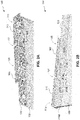
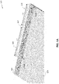
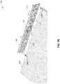
- FIG. 5A illustrates an antenna system 500 according to an exemplary aspect of the present disclosure.
- FIG. 5B illustrates the antenna system 500 having the area 522 of the PCB 520 removed.
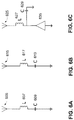
- the first radiator 505, the second radiator 510 and the electromagnetic coupler 515 can be represented by the circuits illustrated in FIGS. 6A-6C , respectively. Because the circuits of FIGS. 6A-6C have been discussed above with respect to FIG. 4 , further discussion with respect to FIGS. 5A and 5B has been omitted for brevity.
- the antenna system 500 includes a first radiator 505, a second radiator 510, and an electromagnetic coupler 515.
- the radiators 505, 510 can be configured to convert one or more electrical signals into electromagnetic waves, and vice versa.
- the electromagnetic coupler 515 can be configured to connect (e.g., couple) a communication device (e.g., transmitter and/or receiver) to one or more of the radiators 505, 510.
- the electromagnetic coupler 515 can include one or more circuits having one or more active and/or passive components that are configured to match the impedance of one or more of the radiators 505, 510.
- the electromagnetic coupler 515 is a capacitive coupler that is configured to capacitively couple one or more of the radiators 505, 510 to one or more communication devices (e.g., transmitter, receiver, etc.).
- the electromagnetic coupler 515 is not limited to being a capacitive coupler and can be configured as an inductive coupler that can inductively couple one or more of the radiators 505, 510.
- the antenna system 500 can be disposed on, for example, a printed circuit board (PCB) 520.
- the PCB 520 can be formed of, for example, glass reinforced epoxy laminate (e.g., FR-4) or one or more other materials as would be understood by one of ordinary skill in the relevant arts.
- the PCB 520 can be included in, for example, a communication device that is configured to use the antenna system 500.
- the radiators 505, 510 and the electromagnetic coupler 515 can be made of one or more metals, one or more metallic compounds, and/or one or more electrically conductive or semi-conductive materials as would be understood by one of ordinary skill in the relevant arts.
- the radiators 505, 510 and the electromagnetic coupler 515 can include one or more active or passive components (e.g. , resistors, inductors, capacitors, etc.) and/or processor circuitry.
- the antenna system 500 can be configured as a transmission antenna system, as a receiving antenna system or as both a transmitting and receiving antenna system.
- two or more of the antenna systems 500 can be implemented within, or used by, a communication device, where one antenna system 500 is configured as a transmission antenna system and another antenna system 500 is configured as a receiving antenna system.
- a first antenna system 500 can be configured on a first side of the PCB 520 as shown in FIG. 1 and a second antenna system 500 can be configured on another side (e.g., a side perpendicular to the first side) of the PCB 520.
- two (or more) of the antenna systems 500 can be implemented within, or used by, a communication device, where the two antenna systems 500 are configured as transmission antennas.
- the two antenna systems 500 can be configured as receiving antennas.
- the first radiator 505 and the second radiator 510 can be configured to be tuned independently within a predetermined frequency range to one or more resonances.
- the first radiator 505 can be configured to primarily operate at lower frequencies within the frequency range (e.g., at a first resonance), while the second radiator 110 can be figured to primarily operate at higher frequencies within the frequency range (e.g., at a second resonance).
- the first and second radiators 505, 510 can be configured to operate at all frequencies within the frequency range.
- the first radiator 505 and/or the second radiator 510 can be configured to implement Carrier Aggregation (CA), including intra-band contiguous (adjacent) CA, intra-band non-contiguous (non-adjacent) CA, and/or inter-band CA.
- CA Carrier Aggregation
- the first radiator 505 has a length L1 that is greater than the length L2 of the second radiator 510.
- the first radiator 105 can have a length of, for example, 23 mm and the second radiator 510 can have a length of, for example, 17 mm.
- the length/width of the first and second radiators 505, 510 can be, for example, 6 mm.
- the width of the radiators 505, 510 can be the same or different.
- first and second radiators 505, 510 and the electromagnetic coupler 515 can be disposed along an edge of the PCB 520.
- first and second radiators 505, 510 and the electromagnetic coupler 515 can be disposed in an area 522 of the PCB 520 in which metallic or other conductive materials have been removed from the PCB 520.
- the first and second radiators 505, 510 and the electromagnetic coupler 515 can be disposed along an edge of the area 522 and/or one or more surfaces (e.g., top, bottom, etc.) of the PCB 520.
- the first radiator 505 and the second radiator 510 can be arranged to have a space or slit 507 formed there between.
- the electromagnetic coupler 515 can be arranged adjacent to the first and second radiators 505, 510 and the space 507.
- the electromagnetic coupler 515 can be adjacent to and spaced from a portion of the first radiator 505 and a portion of the second radiator 510 whose respective edges define the space 507.
- the electromagnetic coupler 515 is spaced from the planar portion of the first radiator 505 (e.g., radiation portion 605), the planar portion of the second radiator 510 (e.g., radiation portion 615), and the space 507 formed between the first and second radiators 505, 510.
- the position of the electromagnetic coupler 515 is not limited to this configuration and may be positioned at other locations along the width of the PCB 520.
- the electromagnetic coupler 515 is spaced from a plane in which the radiation portions 605 and 615 reside. That is, there is an air gap between the electromagnetic coupler 515 and the radiation portions 605 and 615.
- the electromagnetic coupler 515 can have a length that is equal or substantially equal to the length of the space 507.
- the electromagnetic coupler 515 can have a length so that the electromagnetic coupler 515 extends from the space 507 along at least a portion of the radiators 505, 510 (e.g., along radiation portions 605 and 615). In this example, there is an air gap between the electromagnetic coupler 515 and the radiation portions 605 and 615.
- the distance between the electromagnetic coupler 515 and the radiation portions 605 and 615 can be the same or different.
- the electromagnetic coupler 515 includes a first portion that is substantially parallel to the top and bottom surfaces of the PCB 520 and a second portion that is substantially parallel to the radiation portions 605, 615 of the radiators 505, 510, respectively.
- the second portion of the electromagnetic coupler 515 extends from the space 507 along at least a portion of the radiation portions 605 and 615.
- the first portion and the second portion of the electromagnetic coupler form an angle of 90° or substantially 90°, but are not limited to this angled configuration.
- FIG. 7 illustrates an antenna system 700 according to an exemplary aspect of the present disclosure. Although example dimensions are shown in FIG. 7 , the exemplary aspects are not limited to these dimensions.
- the antenna system 700 includes a first radiator 705, a second radiator 710, and an electromagnetic coupler 715.
- the radiators 705, 710 can be configured to convert one or more electrical signals into electromagnetic waves, and vice versa.
- the electromagnetic coupler 715 can be configured to connect (e.g., couple) a communication device ( e.g. , transmitter and/or receiver) to one or more of the radiators 705, 710.
- the electromagnetic coupler 715 can include one or more circuits having one or more active and/or passive components that are configured to match the impedance of one or more of the radiators 705, 710.
- the electromagnetic coupler 715 is a capacitive coupler that is configured to capacitively couple one or more of the radiators 705, 710 to one or more communication devices ( e.g. , transmitter, receiver, etc.).
- the electromagnetic coupler 715 is not limited to being a capacitive coupler and can be configured as an inductive coupler that can inductively couple one or more of the radiators 705, 710.
- the antenna system 700 can be disposed on, for example, a printed circuit board (PCB) 720.
- the PCB 720 can be formed of, for example, glass reinforced epoxy laminate (e.g., FR-4) or one or more other materials as would be understood by one of ordinary skill in the relevant arts.
- the PCB 720 can be included in, for example, a communication device that is configured to use the antenna system 700.
- the radiators 705, 710 and the electromagnetic coupler 715 can be made of one or more metals, one or more metallic compounds, and/or one or more electrically conductive or semi-conductive materials as would be understood by one of ordinary skill in the relevant arts.
- the radiators 705, 710 and the electromagnetic coupler 715 can include one or more active or passive components (e.g. , resistors, inductors, capacitors, etc.) and/or processor circuitry.
- the antenna system 700 can be configured as a transmission antenna system, as a receiving antenna system or as both a transmitting and receiving antenna system. Further, two or more of the antenna systems 700 can be implemented within, or used by, a communication device, where one antenna system 700 is configured as a transmission antenna system and another antenna system 700 is configured as a receiving antenna system.
- a first antenna system 700 can be configured on a first side of the PCB 720 as shown in FIG. 7 and a second antenna system 700 can be configured on another side (e.g., a side perpendicular to the first side) of the PCB 720.
- the first radiator 705 and the second radiator 710 can be configured to be tuned independently within a predetermined frequency range to one or more resonances.
- the first radiator 705 can be configured to primarily operate at lower frequencies within the frequency range (e.g., at a first resonance), while the second radiator 110 can be figured to primarily operate at higher frequencies within the frequency range (e.g., at a first resonance).
- the first and second radiators 705, 710 can be configured to operate at all frequencies within the frequency range.
- each of the radiators 705 and 710 can be configured to address the lower or the upper band.
- the first radiator 705 and/or the second radiator 710 can be configured to implement Carrier Aggregation (CA), including intra-band contiguous (adjacent) CA, intra-band non-contiguous (non-adjacent) CA, and/or inter-band CA.
- CA Carrier Aggregation
- the first radiator 705 and the second radiator 710 can have a length of, for example, 25 mm.
- the height of the radiators 705, 710 can be, for example, 4 mm.
- the radiators 705, 710 have a bent portion that is arranged substantially parallel to the top surface of the PCB 720. The bent portion and have a width of, for example, 2 mm.
- a space 709 can be formed between the radiators 705, 710 that has a length of, for example, 4 mm.
- the dimensions should not be limited to these exemplary values, and the first radiator 705 and/or the second radiator 710 can have other dimensions as would be understood by one of ordinary skill in the relevant arts.
- the lengths of the first radiator 705 and the second radiator 710 can have different dimensions from each other such that one of the radiators 705, 710 is longer than the other.
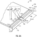
- FIG. 8A illustrates antenna system 700 and a circuit diagram of the radiators 705 and 710 according to an exemplary aspect of the present disclosure.
- the electromagnetic coupler 715 has been removed to expose the connections of the radiators 705, 710 to the PCB 720.
- example dimensions are shown in FIG. 8A , the exemplary aspects are not limited to these dimensions.
- the first radiator 705 includes a first radiation portion 706 that is connected to the PCB 720 via leads 707A and 707B.
- the first radiator 705 can include a capacitor 725A is connected between the lead 707A and ground of the PCB 720.
- the other end of the first radiation portion 706 can be connected to ground of the PCB 720 via lead 707B.
- the capacitor 725A can be a tunable capacitor.
- the capacitor 725A can be a fixed capacitor in one or more of the aspects.
- the capacitor 725A can have a capacitance of, for example, 0.8-5 pF, 0.9-5 pF, 0.92-4.61 pF, 1.73-4.49 pF, 1.73-3.89 pF, 0.92 pF, 1.73 pF, 2.03 pF, 2.93 pF, 3.23 pF, or one or more other capacitances or tunable capacitance ranges as would be understood by those skilled in the relevant arts.
- the second radiator 710 includes a second radiation portion 711 that is connected to the PCB 720 via leads 712A and 712B.
- the second radiator 710 can include a capacitor 725B is connected between the lead 712A and ground of the PCB 720.
- the other end of the second radiation portion 711 can be connected to ground of the PCB 720 via lead 712B.
- the capacitor 725B can be a tunable capacitor.
- the capacitor 725B can be a fixed capacitor in one or more of the aspects.
- the capacitor 725B can have a capacitance of, for example, 0.8-5 pF, 0.9-5 pF, 0.92-4.61 pF, 1.73-3.89 pF, 0.92 pF, 1.73 pF, 2.03 pF, 2.93 pF, 3.23 pF, or one or more other capacitances or tunable capacitance ranges as would be understood by those skilled in the relevant arts.
- the capacitance of capacitor 725A can be the same or different from the capacitance of capacitor 725B.
- FIG. 8B illustrates antenna system 700 and a circuit diagram of electromagnetic coupler 715 according to an exemplary aspect of the present disclosure.
- the electromagnetic coupler 715 can include a coupling portion 730 that is disposed on a portion of the PCB 720, the space 709, a portion of the first radiator 705 and a portion of the second radiator 710.
- the coupling portion 730 is a planar-shaped device as illustrated in FIG. 8B .
- the coupling portion 730 is connected to a feed 755 via one or more active or passive components (e.g., one or more capacitors, inductors, resistors, etc.).
- the coupling portion 730 can be connected to feed 755 via a capacitor 745 and capacitor 750 that are connected in parallel.
- capacitor 745 is a fixed capacitor and the capacitor 750 is a tunable capacitor.
- the capacitors 745 and 750 can both be fixed, both be tunable, or one can be fixed while the other is tunable.
- the coupling portion 730 can be further connected to ground via one or more other active or passive components (e.g., one or more capacitors, inductors, resistors, etc.) that are connected between ground and the electrical node between the feed 755 and the capacitors 745 and 750.
- active or passive components e.g., one or more capacitors, inductors, resistors, etc.
- inductor 735 and capacitor 740 are connected in parallel and between ground and the electrical node between the feed 755 and the capacitors 745 and 750.
- the capacitor 740 is a tunable capacitor.
- the capacitor 740 can be fixed in one or more of the exemplary aspects.
- the inductor 735, capacitors 740, 745 and 750, and feed 755 can be collectively illustrated by 760 in FIG. 8B .
- the coupling portion is connected to ground via capacitors 745 and 750 connected in parallel and inductor 735 and capacitor 740 connected in parallel and in series with the capacitors 745 and 750.
- the feed 755 is connected between ground and the electrical node formed between the capacitors 745 and 750 connected in parallel and inductor 735 and capacitor 740 connected in parallel.
- inductor 735 can have an inductance of, for example, 8 nH, 8.2 nH, 8.5 nH, 9 nH, or one or more other inductances as would be understood by those skilled in the relevant arts.
- the capacitor 740 can have a capacitance of, for example, 0.8-7 pF, 0.9-6 pF, 1.25-6 pF, 1.38-6 pF, or one or more other capacitances or tunable capacitance ranges as would be understood by those skilled in the relevant arts.
- the capacitor 745 can have a capacitance of, for example, 1 pF, 2 pF, 2.4 pF, 2.5 pF, or one or more other capacitances or tunable capacitance ranges as would be understood by those skilled in the relevant arts.
- the capacitor 750 can have a capacitance of, for example, 0.1-2 pF, 0.15-2 pF, 0.16-1.96 pF, or one or more other capacitances or tunable capacitance ranges as would be understood by those skilled in the relevant arts.
- the value of the capacitors 740, 745 and/or 750, and/or the value of the inductor 735 are a function of the dimensions of the coupler 715. In exemplary aspects in which the coupler 715 is designed with different dimensions, the values of in the circuitry (values of the capacitors 740, 745 and/or 750, and/or the value of the inductor 735) can be adjusted accordingly.
- references in the specification to "one aspect,” “an aspect,” “an exemplary aspect,” etc., indicate that the aspect described may include a particular feature, structure, or characteristic, but every aspect may not necessarily include the particular feature, structure, or characteristic. Moreover, such phrases are not necessarily referring to the same aspect. Further, when a particular feature, structure, or characteristic is described in connection with an aspect, it is submitted that it is within the knowledge of one skilled in the art to affect such feature, structure, or characteristic in connection with other aspects whether or not explicitly described.
- a machine-readable medium may include any mechanism for storing or transmitting information in a form readable by a machine (e.g. , a computing device).
- a machine-readable medium may include read only memory (ROM); random access memory (RAM); magnetic disk storage media; optical storage media; flash memory devices; electrical, optical, acoustical or other forms of propagated signals (e.g. , carrier waves, infrared signals, digital signals, etc.), and others.
- firmware, software, routines, instructions may be described herein as performing certain actions. However, it should be appreciated that such descriptions are merely for convenience and that such actions in fact results from computing devices, processors, controllers, or other devices executing the firmware, software, routines, instructions, etc. Further, any of the implementation variations may be carried out by a general purpose computer.
- processor circuitry shall be understood to be circuit(s), processor(s), logic, code, or a combination thereof.
- a circuit can include an analog circuit, a digital circuit, state machine logic, other structural electronic hardware, or a combination thereof.
- a processor can include a microprocessor, a digital signal processor (DSP), or other hardware processor.
- DSP digital signal processor
- the processor can be "hard-coded” with instructions to perform corresponding function(s) according to aspects described herein.
- the processor can access an internal and/or external memory to retrieve instructions stored in the memory, which when executed by the processor, perform the corresponding function(s) associated with the processor, and/or one or more functions and/or operations related to the operation of a component having the processor included therein.
- module shall be understood to include one of software, firmware, hardware (such as circuits, microchips, processors, or devices, or any combination thereof), or any combination thereof.
- each module can include one or more components within an actual device, and each component that forms a part of the described module can function either cooperatively or independently of any other component forming a part of the module.
- multiple modules described herein can represent a single component within an actual device. Further, components within a module can be in a single device or distributed among multiple devices in a wired or wireless manner.
Landscapes
- Engineering & Computer Science (AREA)
- Computer Networks & Wireless Communication (AREA)
- Near-Field Transmission Systems (AREA)
- Support Of Aerials (AREA)
Abstract
Description
- Aspects described herein generally relate to antennas, including one or more tunable antennas.
- Wireless communication environments can use multi-antenna techniques that include multiple antennas at a transmitter, receiver, and/or transceiver. The multi-antenna techniques can be grouped into three different categories: diversity, interference suppression, and spatial multiplexing. These three categories are often collectively referred to as Multiple-input Multiple-output (MIMO) communication even though not all of the multi-antenna techniques that fall within these categories require at least two antennas at both the transmitter and receiver.
- Carrier Aggregation (CA) is a feature of a mobile communication standard, such as, Release-10 of the 3GPP LTE-Advanced standard, which allows multiple resource blocks from/to multiple respective serving cells to be logically grouped together (aggregated) and allocated to the same wireless communication device. The aggregated resource blocks are known as component carriers (CCs) in the LTE-Advanced standard. Each of the wireless communication devices may receive/transmit multiple component carriers simultaneously from/to the multiple respective serving cells, thereby effectively increasing the downlink/uplink bandwidth of the wireless communication device(s). The term "component carriers (CCs)" is used to refer to groups of resource blocks (defined in terms or frequency and/or time) of two or more RF carriers that are aggregated (logically grouped) together.
- There are various forms of Carrier Aggregation (CA) as defined by Release-10 of the LTE-Advanced standard, including intra-band contiguous (adjacent) CA, intra-band non-contiguous (non-adjacent) CA, and inter-band CA. In intra-band contiguous CA, aggregated component carriers (CCs) are within the same frequency band and adjacent to each other forming a contiguous frequency block. In intra-band non- contiguous CA, aggregated CCs are within the same frequency band but are not adjacent to each other. In inter-band CA, aggregated CCs are in different frequency bands.
- Release-10 of the LTE-Advanced standard allows a maximum of five CCs to be allocated to a wireless communication device at any given time. CCs can vary in size from 1.4 to 20 MHz, resulting in a maximum bandwidth of 100 MHz that can be allocated to the wireless communication device in the downlink/uplink. The allocation of CCs to the wireless communication device is performed by the network and is communicated to the wireless communication device.
- The accompanying drawings, which are incorporated herein and form a part of the specification, illustrate the aspects of the present disclosure and, together with the description, further serve to explain the principles of the aspects and to enable a person skilled in the pertinent art to make and use the aspects.
-
FIG. 1 illustrates an antenna system according to an exemplary aspect of the present disclosure. -
FIG. 2A illustrates a front prospective view of the antenna system illustrated inFIG. 1 . -
FIG. 2B illustrates a back prospective view of the antenna system illustrated inFIG. 1 . -
FIG. 2C illustrates another front prospective view of the antenna system illustrated inFIG. 1 . -
FIGS. 3A and 3B illustrate circuit diagrams of radiators according to exemplary aspects of the present disclosure. -
FIG. 3C illustrates a circuit diagram of an electromagnetic coupler according to an exemplary aspect of the present disclosure. -
FIG. 4 illustrates an antenna system according to an exemplary aspect of the present disclosure. -
FIGS. 5A and5B illustrate antenna systems according to exemplary aspects of the present disclosure. -
FIGS. 6A and 6B illustrate circuit diagrams of radiators according to exemplary aspects of the present disclosure. -
FIG. 6C illustrates a circuit diagram of an electromagnetic coupler according to an exemplary aspect of the present disclosure. -
FIG. 7 illustrates an antenna system according to an exemplary aspect of the present disclosure. -
FIG. 8A illustrates an antenna system and corresponding circuit diagram according to an exemplary aspect of the present disclosure. -
FIG. 8B illustrates an antenna system and corresponding circuit diagram according to an exemplary aspect of the present disclosure. - The exemplary aspects of the present disclosure will be described with reference to the accompanying drawings. The drawing in which an element first appears is typically indicated by the leftmost digit(s) in the corresponding reference number.
- In the following description, numerous specific details are set forth in order to provide a thorough understanding of the aspects of the present disclosure. However, it will be apparent to those skilled in the art that the aspects, including structures, systems, and methods, may be practiced without these specific details. The description and representation herein are the common means used by those experienced or skilled in the art to most effectively convey the substance of their work to others skilled in the art. In other instances, well-known methods, procedures, components, and circuitry have not been described in detail to avoid unnecessarily obscuring aspects of the disclosure.
- In the following disclosure, one or more exemplary aspects can be implemented using wireless communications conforming to the Long-Term Evolution (LTE) and/or LTE Advanced standards. The LTE and LTE Advanced standards are developed by the 3rd Generation Partnership Project (3GPP) and described in the 3GPP Technical Specification 36 standard titled "Evolved Universal Terrestrial Radio Access (E-UTRA); Physical layer procedures," and the International Mobile Telecomunnications-2000 (IMT-2000) and IMT Advanced standards, all of which are incorporated herein by reference in their entirety.
- As will be apparent to a person of ordinary skill in the art based on the teachings herein, exemplary aspects are not limited to the LTE and/or LTE Advanced standards, and can be applied to other cellular communication standards, including (but not limited to), Evolved High-Speed Packet Access (HSPA+), Wideband Code Division Multiple Access (W-CDMA), CDMA2000, Time Division-Synchronous Code Division Multiple Access (TD-SCDMA), Global System for Mobile Communications (GSM), General Packet Radio Service (GPRS), Enhanced Data Rates for GSM Evolution (EDGE), and/or Worldwide Interoperability for Microwave Access (WiMAX) (IEEE 802.16), and/or to one or more non-cellular communication standards, including (but not limited to) WLAN (IEEE 802.11), Bluetooth, Near-field Communication (NFC) (ISO/IEC 18092), ZigBee (IEEE 802.15.4), and/or Radio-frequency identification (RFID). These various standards and/or protocols are each incorporated herein by reference in their entirety.
-
FIG. 1 illustrates anantenna system 100 according to an exemplary aspect of the present disclosure. In an exemplary aspect, theantenna system 100 includes afirst radiator 105, asecond radiator 110, and anelectromagnetic coupler 115. Theradiators electromagnetic coupler 115 can be configured to connect (e.g., couple) a communication device (e.g., transmitter and/or receiver) to one or more of theradiators electromagnetic coupler 115 can include one or more circuits having one or more active and/or passive components that are configured to match the impedance of one or more of theradiators electromagnetic coupler 115 is an inductive coupler that is configured to inductively couple one or more of theradiators electromagnetic coupler 115 is not limited to being an inductive coupler and can be configured as a capacitive coupler that can capacitively couple one or more of theradiators antenna system 100 can be configured as a transmission antenna system, as a receiving antenna system or as both a transmitting and receiving antenna system. Further, two or more of theantenna systems 100 can be implemented within, or used by, a communication device, where oneantenna system 100 is configured as a transmission antenna system and anotherantenna system 100 is configured as a receiving antenna system. For example, afirst antenna system 100 can be configured on a first side of thePCB 120 as shown inFIG. 1 and asecond antenna system 100 can be configured on another side (e.g., a side perpendicular to the first side) of thePCB 120. Further, two (or more) of theantenna systems 100 can be implemented within, or used by, a communication device, where the twoantenna systems 100 are configured as transmission antennas. Similarly, the twoantenna systems 100 can be configured as receiving antennas. - The
antenna system 100 can be disposed on, for example, a printed circuit board (PCB) 120. ThePCB 120 can be formed of, for example, glass reinforced epoxy laminate (e.g., FR-4) or one or more other materials as would be understood by one of ordinary skill in the relevant arts. ThePCB 120 can be included in, for example, a communication device that is configured to use theantenna system 100. In an exemplary aspect, theradiators electromagnetic coupler 115 can be made of one or more metals, one or more metallic compounds, and/or one or more electrically conductive or semi-conductive materials as would be understood by one of ordinary skill in the relevant arts. Theradiators electromagnetic coupler 115 can include one or more active or passive components (e.g., resistors, inductors, capacitors, etc.) and/or processor circuitry. - In an exemplary aspect, the
first radiator 105 and thesecond radiator 110 can be configured to be tuned independently within a predetermined frequency range to one or more resonances. In an exemplary aspect, the frequency range can be, for example, 700 MHz to 960 MHz, but is not limited to this exemplary range. For example, thefirst radiator 105 can be configured to primarily operate at lower frequencies within the frequency range (e.g., at a first resonance), while thesecond radiator 110 can be figured to primarily operate at higher frequencies within the frequency range (e.g., at a second resonance). Although primarily operating at respective subsets of frequencies within the frequency range, the first andsecond radiators first radiator 105 and/or thesecond radiator 110 can be configured to implement Carrier Aggregation (CA), including intra-band contiguous (adjacent) CA, intra-band non-contiguous (non-adjacent) CA, and/or inter-band CA. - In an exemplary aspect, the
first radiator 105 has a length L1 that is greater than the length L2 of thesecond radiator 110. For example, thefirst radiator 105 can have a length of, for example, 23 mm and thesecond radiator 110 can have a length of, for example, 17 mm. The width of the first andsecond radiators radiators space 107 between the first andsecond radiators first radiator 105, thesecond radiator 110, and thespace 107 can have other dimensions as would be understood by one of ordinary skill in the relevant arts. - As illustrated in
FIG. 1 , the first andsecond radiators electromagnetic coupler 115 can be disposed along an edge of thePCB 120. For example, first andsecond radiators electromagnetic coupler 115 can be disposed in anarea 122 of thePCB 120 in which metallic or other conductive materials have been removed from thePCB 120. In this example, the first andsecond radiators area 122 and/or one or more surfaces (e.g., top, bottom, etc.) of thePCB 120, and theelectromagnetic coupler 115 can be disposed on one or more surfaces (e.g., top, bottom, etc.) of thePCB 120. Alternatively, thearea 122 can represent a portion of thePCB 120 that has been removed. In this example, the first andsecond radiators electromagnetic coupler 115 can be configured to extend from an edge of thePCB 120 and within thearea 122 in which a portion of thePCB 120 has been removed. The arrangement of the first andsecond radiators electromagnetic coupler 115 is described below with reference toFIGS. 2A-2C . - In an exemplary aspect, the
first radiator 105 and thesecond radiator 110 can be arranged to have a space or slit 107 formed there between. Further, theelectromagnetic coupler 115 can be arranged adjacent to the first andsecond radiators space 107. For example, theelectromagnetic coupler 115 can be adjacent to and spaced from a portion of thefirst radiator 105 and a portion of thesecond radiator 110 whose adjacent edges define thespace 107. In this configuration, theelectromagnetic coupler 115 is spaced from the planar portion of thefirst radiator 105, the planar portion of thesecond radiator 110, and thespace 107 formed between the first andsecond radiators electromagnetic coupler 115 is not limited to this configuration and may be positioned at other locations along the width of thePCB 120. -
FIGS. 2A and 2B illustrate a front prospective view and a back prospective view of theantenna system 100 illustrated inFIG. 1 , respectively. With reference toFIG. 2A , theelectromagnetic coupler 115 is disposed on a front side of thePCB 120 in thearea 122. With reference toFIG. 2B , theradiators area 122 of thePCB 120.FIG. 2C illustrates a front prospective view of theantenna system 100 in which thearea 122 of thePCB 120 has been removed. - In an exemplary aspect, the
first radiator 105 can be electrically connected to thePCB 120 vialead 210A extending from a first edge of thefirst radiator 105 and a lead 210B extending from a second edge of thefirst radiator 105. In an exemplary aspect, thefirst radiator 105 includes acapacitor 215A electrically connected between thePCB 120 and thelead 211A. In one or more exemplary aspects, thelead 210A and/or lead 210B can be connected to the PCB via one or more capacitors, inductors, and/or resistors. Alternatively, thelead 210A and/or lead 210B can be connected to the PCB directly. -
FIG. 3A illustrates a circuit diagram ofradiator 105 according to an exemplary aspect of the present disclosure. In an exemplary aspect, thefirst radiator 105 includes afirst radiation portion 305 having a first end connected to ground and a second end connected to ground via acapacitor 310. In one or more exemplary aspects, the first end of thefirst radiation portion 305 can be connected to ground via one or more capacitors, inductors, and/or resistors. For example, with reference toFIG. 2B , thefirst radiator 105 can be connected to ground on thePCB 120 vialead 210A and to acapacitor 215A vialead 211A, where thecapacitor 215A is further connected to ground on thePCB 120. In one or more exemplary aspects, thefirst radiator 105 can be connected to ground via one or more capacitors, inductors, and/or resistors. In an exemplary aspect, thecapacitor 215A (310 inFIG. 3A ) can be a fixed or tunable capacitor. In an exemplary aspect, thecapacitor 215A (310 inFIG. 3A ) can have a capacitance of, for example, 1-5 pF, 1-3 pF, 2-3 pF, or one or more other capacitances or tunable capacitance ranges as would be understood by those skilled in the relevant arts. - In an exemplary aspect, the
second radiator 110 can be electrically connected to thePCB 120 vialead 210B extending from a first edge of thesecond radiator 110 and a lead 211B (as shown inFIG. 2B ) extending from a second edge of thesecond radiator 110. In an exemplary aspect, thesecond radiator 110 includes acapacitor 215B electrically connected between thePCB 120 and the lead 211B. -
FIG. 3B illustrates a circuit diagram of thesecond radiator 110 according to an exemplary aspect of the present disclosure. In an exemplary aspect, thesecond radiator 110 includes afirst radiation portion 315 having a first end connected to ground and a second end connected to ground via acapacitor 320. For example, with reference toFIG. 2B , thesecond radiator 110 can be connected to ground on thePCB 120 vialead 210B and to acapacitor 215B vialead 211B, where thecapacitor 215B is further connected to ground on thePCB 120. In an exemplary aspect, thecapacitor 215B (320 inFIG. 3B ) can be a fixed or tunable capacitor. In an exemplary aspect, thecapacitor 215B (320 inFIG. 3B ) can have a capacitance of, for example, 1-5 pF, 1-3 pF, 2-3 pF, or one or more other capacitances or tunable capacitance ranges as would be understood by those skilled in the relevant arts. In an exemplary aspect, the capacitance ofcapacitor 215B (320 inFIG. 3B ) can be the same or different from the capacitance ofcapacitor 215A (310 inFIG. 3A ). - With reference to
FIG. 2A , theelectromagnetic coupler 115 can be electrically connected to thePCB 120 via a feed and one or more passive components (e.g., capacitors, inductors, resistors, etc.) represented as 205 inFIG. 2A . For example, with reference toFIG. 3C , theelectromagnetic coupler 115 can include twocapacitors coupling portion 340. Thecoupling portion 340 includes a first end electrically connected to ground and a second end electrically connected to ground viacapacitor 335 and to feed 325 viacapacitor 330. In an exemplary aspect, the first end of thecoupling portion 340 can be connected to ground via one or more passive components (e.g., capacitors, inductors, resistors, etc.). Thecapacitors capacitors capacitors - With reference to
FIG. 2C , thecapacitors capacitor 215A and thecapacitor 215B associated with theradiators capacitors capacitor 215A, and thecapacitor 215B can be implemented in a single chip. A single-chip implementation can be used to reduce the cost of the exemplary aspect. The capacitors are not limited to a single-chip implementation and the capacitors can be implemented in two or more chips. -
FIG. 4 illustrates anantenna system 400 according to an exemplary aspect of the present disclosure. In an exemplary aspect, theantenna system 400 includes afirst radiator 405, asecond radiator 410, and anelectromagnetic coupler 415. Theradiators electromagnetic coupler 415 can be configured to connect (e.g., couple) a communication device (e.g., transmitter and/or receiver) to one or more of theradiators electromagnetic coupler 415 can include one or more circuits having one or more active and/or passive components that are configured to match the impedance of one or more of theradiators electromagnetic coupler 415 is a capacitive coupler that is configured to capacitively couple one or more of theradiators electromagnetic coupler 415 is not limited to being a capacitive coupler and can be configured as an inductive coupler that can inductively couple one or more of theradiators - The
antenna system 400 can be disposed on, for example, a printed circuit board (PCB) 420. ThePCB 420 can be formed of, for example, glass reinforced epoxy laminate (e.g., FR-4) or one or more other materials as would be understood by one of ordinary skill in the relevant arts. ThePCB 420 can be included in, for example, a communication device that is configured to use theantenna system 400. In an exemplary aspect, theradiators electromagnetic coupler 415 can be made of one or more metals, one or more metallic compounds, and/or one or more electrically conductive or semi-conductive materials as would be understood by one of ordinary skill in the relevant arts. Theradiators electromagnetic coupler 415 can include one or more active or passive components (e.g., resistors, inductors, capacitors, etc.) and/or processor circuitry. - In an exemplary aspect, the
antenna system 400 can be configured as a transmission antenna system, as a receiving antenna system or as both a transmitting and receiving antenna system. Further, two or more of theantenna systems 400 can be implemented within, or used by, a communication device, where oneantenna system 100 is configured as a transmission antenna system and anotherantenna system 400 is configured as a receiving antenna system. For example, afirst antenna system 400 can be configured on a first side of thePCB 420 as shown inFIG. 4 and asecond antenna system 400 can be configured on another side (e.g., a side perpendicular to the first side) of thePCB 420. In one or more aspects, two (or more) of theantenna systems 100 can be implemented within, or used by, a communication device, where the twoantenna systems 100 are configured as transmission antennas. Similarly, the twoantenna systems 100 can be configured as receiving antennas. - In an exemplary aspect, the
first radiator 405 and thesecond radiator 410 can be configured to be tuned independently within a predetermined frequency range to one or more resonances. For example, thefirst radiator 405 can be configured to primarily operate at lower frequencies within the frequency range (e.g., at a first resonance), while thesecond radiator 110 can be figured to primarily operate at higher frequencies within the frequency range (e.g., at a second resonance). Although primarily operating at respective subsets of frequencies within the frequency range, the first andsecond radiators first radiator 405 and/or thesecond radiator 410 can be configured to implement Carrier Aggregation (CA), including intra-band contiguous (adjacent) CA, intra-band non-contiguous (non-adjacent) CA, and/or inter-band CA. - In an exemplary aspect, the
first radiator 405 has a length L1 that is greater than the length L2 of thesecond radiator 410. For example, thefirst radiator 105 can have a length of, for example, 19.5 mm and thesecond radiator 410 can have a length of, for example, 16.5 mm. The width of the first andsecond radiators radiators first radiator 405 and/or thesecond radiator 410 can have other dimensions as would be understood by one of ordinary skill in the relevant arts. - As illustrated in
FIG. 4 , the first andsecond radiators electromagnetic coupler 415 can be disposed along an edge of thePCB 120. For example, first andsecond radiators electromagnetic coupler 115 can be disposed in anarea 422 of thePCB 420 in which metallic or other conductive materials have been removed from thePCB 420. In this example, the first andsecond radiators electromagnetic coupler 415 can be disposed along an edge of thearea 422 and/or one or more surfaces (e.g., top, bottom, etc.) of thePCB 420. Theelectromagnetic coupler 415 can have a length of, for example, 3 mm and be spaced from the each of theradiators spaces electromagnetic coupler 415 and theradiators first radiator 405, thesecond radiator 410,electromagnetic coupler 415, and/or one or both of thespaces - In an exemplary aspect, the
radiators electromagnetic coupler 415 can be arranged such that a space or slit 407 is formed between theelectromagnetic coupler 415 and thefirst radiator 405, and a space or slit 408 is formed between theelectromagnetic coupler 415 and thesecond radiator 410. Further, theelectromagnetic coupler 415 can be disposed in the same or substantially the same plane as theradiators electromagnetic coupler 415 can be disposed on the edge of thearea 422 and in between theradiators area 422. In this example, adjacent edges of thefirst radiator 405 and theelectromagnetic coupler 415 define thespace 407 and adjacent edges of thesecond radiator 410 and theelectromagnetic coupler 415 define thespace 408. - With continued reference to
FIG. 4 and with reference toFIGS. 6A-6C , thefirst radiator 405 can include afirst radiation portion 605 that is connected to ground vialead 406 and one or more components (e.g., one or more inductors, capacitors, and/or resistors). In an exemplary aspect, thefirst radiation portion 605 is connected to ground via aninductor 607 and acapacitor 609 connected in series. In this configuration, a first end of theradiation portion 605 of thefirst radiator 405 is floating while a second end of theradiation portion 605 that is opposite the first end is connected to thelead 406 and the one or more components (e.g.,inductor 607 and acapacitor 609 connected in series). Theinductor 607 andcapacitor 609 are represented by 430A inFIG. 4 . In an exemplary aspect, thecapacitor 609 is a tunable capacitor. However, thecapacitor 609 can be a fixed capacitor in one or more of the aspects. In an exemplary aspect, theinductor 607 can have an inductance of, for example, 1-100 nH, 1-50 nH, 10-50 nH, 20-45 nH, 35-45 nH, 44 nH, or another inductance value as would be understood by those skilled in the relevant arts. Theinductor 607 is not limited to this example inductance and can another inductance value as would be understood by those skilled in the relevant arts. Thecapacitor 609 can have a capacitance of, for example, 1-5 pF, 1-4.5 pF, 1-3 pF, 2-4 pF, or one or more other capacitances or tunable capacitance ranges as would be understood by those skilled in the relevant arts. - Similarly, the
second radiator 410 can include asecond radiation portion 615 that is connected to ground vialead 411 and one or more components (e.g., one or more inductors, capacitors, and/or resistors). In an exemplary aspect, thesecond radiation portion 615 is connected to ground via aninductor 617 and acapacitor 619 connected in series. In this configuration, a first end of theradiation portion 615 of thefirst radiator 410 is floating while a second end of theradiation portion 615 that is opposite the first end is connected to thelead 411 and the one or more components (e.g.,inductor 617 and acapacitor 619 connected in series). Theinductor 617 andcapacitor 619 are represented by 430B inFIG. 4 . In an exemplary aspect, thecapacitor 619 is a tunable capacitor. However, thecapacitor 619 can be a fixed capacitor in one or more of the aspects. In an exemplary aspect, theinductor 617 can have an inductance of, for example, 1-100 nH, 1-50 nH, 10-50 nH, 20-45 nH, 35-45 nH, or 41 nH. Theinductor 617 is not limited to this example inductance and can have another inductance value as would be understood by those skilled in the relevant arts. Thecapacitor 619 can have a capacitance of, for example, 1-5 pF, 1-4.5 pF, 1-3 pF, 2-4 pF, or one or more other capacitances or tunable capacitance ranges as would be understood by those skilled in the relevant arts. - The
electromagnetic coupler 415 can include acoupling portion 625 that is connected to ground via one or more components (e.g., one or more inductors, capacitors, and/or resistors) and lead 416. In an exemplary aspect, the coupling portion is connected to ground via aninductor 627 and acapacitor 629 connected in series. Thecoupling portion 625 can also be connected to afeed 635 via theinductor 627. In this example, thefeed 635,inductor 627 andcapacitor 629 are represented by 412 located at the end oflead 416 as shown inFIG. 4 . In an exemplary, theelectromagnetic coupler 415 is a capacitive coupler. Theelectromagnetic coupler 415 is not limited to being a capacitive coupler and can be configured as an inductive coupler. In an exemplary aspect, thecapacitor 629 is a fixed capacitor. However, thecapacitor 629 can be a tunable capacitor in one or more of the aspects. Thecapacitor 629 can have a capacitance of, for example, 1-20 pF, 1-10 pF, 1-5 pF, 2-4 pF, 3-4.5 pF, 3.5-4.5 pF, 4 pF, or one or more other capacitances or tunable capacitance ranges as would be understood by those skilled in the relevant arts. In an exemplary aspect, theinductor 627 can have an inductance of, for example, 1-100 nH, 1-50 nH, 1-10 nH, 10-50 nH, 20-45 nH, 35-45 nH, or 6 nH. Theinductor 627 is not limited to this example inductance and can another inductance value as would be understood by those skilled in the relevant arts. - In an exemplary aspect, the
inductor 607 and capacitor 609 (i.e., 430A) and/or theinductor 617 and capacitor 619 (i.e., 430B) can be located adjacent to thefeed 635,inductor 627 andcapacitor 629 represented as 412. In this configuration, theinductor 607,capacitor 609,inductor 617,capacitor 619, feed 635,inductor 627 andcapacitor 629 can be implemented in a single chip. The components can also be implemented on a plurality of chips, where one or more of the chips include two or more of the components. In these examples, the leads connecting theradiation portions PCB 420. For example, 430A located near 412 can have a wire running along thePCB 420 to the lead connecting to theradiator 405. A similar configuration can be used for 430B and thesecond radiator 410. -
FIG. 5A illustrates anantenna system 500 according to an exemplary aspect of the present disclosure.FIG. 5B illustrates theantenna system 500 having thearea 522 of thePCB 520 removed. In an exemplary aspect, thefirst radiator 505, thesecond radiator 510 and theelectromagnetic coupler 515 can be represented by the circuits illustrated inFIGS. 6A-6C , respectively. Because the circuits ofFIGS. 6A-6C have been discussed above with respect toFIG. 4 , further discussion with respect toFIGS. 5A and5B has been omitted for brevity. - In an exemplary aspect, the
antenna system 500 includes afirst radiator 505, asecond radiator 510, and anelectromagnetic coupler 515. Theradiators electromagnetic coupler 515 can be configured to connect (e.g., couple) a communication device (e.g., transmitter and/or receiver) to one or more of theradiators electromagnetic coupler 515 can include one or more circuits having one or more active and/or passive components that are configured to match the impedance of one or more of theradiators electromagnetic coupler 515 is a capacitive coupler that is configured to capacitively couple one or more of theradiators electromagnetic coupler 515 is not limited to being a capacitive coupler and can be configured as an inductive coupler that can inductively couple one or more of theradiators - The
antenna system 500 can be disposed on, for example, a printed circuit board (PCB) 520. ThePCB 520 can be formed of, for example, glass reinforced epoxy laminate (e.g., FR-4) or one or more other materials as would be understood by one of ordinary skill in the relevant arts. ThePCB 520 can be included in, for example, a communication device that is configured to use theantenna system 500. In an exemplary aspect, theradiators electromagnetic coupler 515 can be made of one or more metals, one or more metallic compounds, and/or one or more electrically conductive or semi-conductive materials as would be understood by one of ordinary skill in the relevant arts. Theradiators electromagnetic coupler 515 can include one or more active or passive components (e.g., resistors, inductors, capacitors, etc.) and/or processor circuitry. - In an exemplary aspect, the
antenna system 500 can be configured as a transmission antenna system, as a receiving antenna system or as both a transmitting and receiving antenna system. Further, two or more of theantenna systems 500 can be implemented within, or used by, a communication device, where oneantenna system 500 is configured as a transmission antenna system and anotherantenna system 500 is configured as a receiving antenna system. For example, afirst antenna system 500 can be configured on a first side of thePCB 520 as shown inFIG. 1 and asecond antenna system 500 can be configured on another side (e.g., a side perpendicular to the first side) of thePCB 520. In one or more aspects, two (or more) of theantenna systems 500 can be implemented within, or used by, a communication device, where the twoantenna systems 500 are configured as transmission antennas. Similarly, the twoantenna systems 500 can be configured as receiving antennas. - In an exemplary aspect, the
first radiator 505 and thesecond radiator 510 can be configured to be tuned independently within a predetermined frequency range to one or more resonances. For example, thefirst radiator 505 can be configured to primarily operate at lower frequencies within the frequency range (e.g., at a first resonance), while thesecond radiator 110 can be figured to primarily operate at higher frequencies within the frequency range (e.g., at a second resonance). Although primarily operating at respective subsets of frequencies within the frequency range, the first andsecond radiators first radiator 505 and/or thesecond radiator 510 can be configured to implement Carrier Aggregation (CA), including intra-band contiguous (adjacent) CA, intra-band non-contiguous (non-adjacent) CA, and/or inter-band CA. - In an exemplary aspect, the
first radiator 505 has a length L1 that is greater than the length L2 of thesecond radiator 510. For example, thefirst radiator 105 can have a length of, for example, 23 mm and thesecond radiator 510 can have a length of, for example, 17 mm. The length/width of the first andsecond radiators radiators first radiator 505 and/or thesecond radiator 510 can have other dimensions as would be understood by one of ordinary skill in the relevant arts. - As illustrated in
FIGS. 5A-5B , the first andsecond radiators electromagnetic coupler 515 can be disposed along an edge of thePCB 520. For example, first andsecond radiators electromagnetic coupler 515 can be disposed in anarea 522 of thePCB 520 in which metallic or other conductive materials have been removed from thePCB 520. In this example, the first andsecond radiators electromagnetic coupler 515 can be disposed along an edge of thearea 522 and/or one or more surfaces (e.g., top, bottom, etc.) of thePCB 520. - In an exemplary aspect, the
first radiator 505 and thesecond radiator 510 can be arranged to have a space or slit 507 formed there between. Further, theelectromagnetic coupler 515 can be arranged adjacent to the first andsecond radiators space 507. For example, theelectromagnetic coupler 515 can be adjacent to and spaced from a portion of thefirst radiator 505 and a portion of thesecond radiator 510 whose respective edges define thespace 507. In this configuration, theelectromagnetic coupler 515 is spaced from the planar portion of the first radiator 505 (e.g., radiation portion 605), the planar portion of the second radiator 510 (e.g., radiation portion 615), and thespace 507 formed between the first andsecond radiators electromagnetic coupler 515 is not limited to this configuration and may be positioned at other locations along the width of thePCB 520. - In an exemplary aspect, the
electromagnetic coupler 515 is spaced from a plane in which theradiation portions electromagnetic coupler 515 and theradiation portions electromagnetic coupler 515 can have a length that is equal or substantially equal to the length of thespace 507. In an exemplary aspect, as illustrated inFIG. 5B , theelectromagnetic coupler 515 can have a length so that theelectromagnetic coupler 515 extends from thespace 507 along at least a portion of theradiators 505, 510 (e.g., alongradiation portions 605 and 615). In this example, there is an air gap between theelectromagnetic coupler 515 and theradiation portions electromagnetic coupler 515 and theradiation portions electromagnetic coupler 515 includes a first portion that is substantially parallel to the top and bottom surfaces of thePCB 520 and a second portion that is substantially parallel to theradiation portions radiators electromagnetic coupler 515 extends from thespace 507 along at least a portion of theradiation portions -
FIG. 7 illustrates anantenna system 700 according to an exemplary aspect of the present disclosure. Although example dimensions are shown inFIG. 7 , the exemplary aspects are not limited to these dimensions. - In an exemplary aspect, the
antenna system 700 includes afirst radiator 705, asecond radiator 710, and anelectromagnetic coupler 715. Theradiators electromagnetic coupler 715 can be configured to connect (e.g., couple) a communication device (e.g., transmitter and/or receiver) to one or more of theradiators electromagnetic coupler 715 can include one or more circuits having one or more active and/or passive components that are configured to match the impedance of one or more of theradiators electromagnetic coupler 715 is a capacitive coupler that is configured to capacitively couple one or more of theradiators electromagnetic coupler 715 is not limited to being a capacitive coupler and can be configured as an inductive coupler that can inductively couple one or more of theradiators - The
antenna system 700 can be disposed on, for example, a printed circuit board (PCB) 720. ThePCB 720 can be formed of, for example, glass reinforced epoxy laminate (e.g., FR-4) or one or more other materials as would be understood by one of ordinary skill in the relevant arts. ThePCB 720 can be included in, for example, a communication device that is configured to use theantenna system 700. In an exemplary aspect, theradiators electromagnetic coupler 715 can be made of one or more metals, one or more metallic compounds, and/or one or more electrically conductive or semi-conductive materials as would be understood by one of ordinary skill in the relevant arts. Theradiators electromagnetic coupler 715 can include one or more active or passive components (e.g., resistors, inductors, capacitors, etc.) and/or processor circuitry. - In an exemplary aspect, the
antenna system 700 can be configured as a transmission antenna system, as a receiving antenna system or as both a transmitting and receiving antenna system. Further, two or more of theantenna systems 700 can be implemented within, or used by, a communication device, where oneantenna system 700 is configured as a transmission antenna system and anotherantenna system 700 is configured as a receiving antenna system. For example, afirst antenna system 700 can be configured on a first side of thePCB 720 as shown inFIG. 7 and asecond antenna system 700 can be configured on another side (e.g., a side perpendicular to the first side) of thePCB 720. - In an exemplary aspect, the
first radiator 705 and thesecond radiator 710 can be configured to be tuned independently within a predetermined frequency range to one or more resonances. For example, thefirst radiator 705 can be configured to primarily operate at lower frequencies within the frequency range (e.g., at a first resonance), while thesecond radiator 110 can be figured to primarily operate at higher frequencies within the frequency range (e.g., at a first resonance). Although primarily operating at respective subsets of frequencies within the frequency range, the first andsecond radiators radiators first radiator 705 and/or thesecond radiator 710 can be configured to implement Carrier Aggregation (CA), including intra-band contiguous (adjacent) CA, intra-band non-contiguous (non-adjacent) CA, and/or inter-band CA. - In an exemplary aspect and with reference to
FIG. 8A , thefirst radiator 705 and thesecond radiator 710 can have a length of, for example, 25 mm. The height of theradiators radiators PCB 720. The bent portion and have a width of, for example, 2 mm. Aspace 709 can be formed between theradiators first radiator 705 and/or thesecond radiator 710 can have other dimensions as would be understood by one of ordinary skill in the relevant arts. In an exemplary aspect, the lengths of thefirst radiator 705 and thesecond radiator 710 can have different dimensions from each other such that one of theradiators -
FIG. 8A illustratesantenna system 700 and a circuit diagram of theradiators radiators electromagnetic coupler 715 has been removed to expose the connections of theradiators PCB 720. Although example dimensions are shown inFIG. 8A , the exemplary aspects are not limited to these dimensions. - In an exemplary aspect, the
first radiator 705 includes afirst radiation portion 706 that is connected to thePCB 720 vialeads first radiator 705 can include acapacitor 725A is connected between the lead 707A and ground of thePCB 720. The other end of thefirst radiation portion 706 can be connected to ground of thePCB 720 vialead 707B. In an exemplary aspect, thecapacitor 725A can be a tunable capacitor. However, thecapacitor 725A can be a fixed capacitor in one or more of the aspects. In an exemplary aspect, thecapacitor 725A can have a capacitance of, for example, 0.8-5 pF, 0.9-5 pF, 0.92-4.61 pF, 1.73-4.49 pF, 1.73-3.89 pF, 0.92 pF, 1.73 pF, 2.03 pF, 2.93 pF, 3.23 pF, or one or more other capacitances or tunable capacitance ranges as would be understood by those skilled in the relevant arts. - In an exemplary aspect, the
second radiator 710 includes asecond radiation portion 711 that is connected to thePCB 720 vialeads second radiator 710 can include acapacitor 725B is connected between the lead 712A and ground of thePCB 720. The other end of thesecond radiation portion 711 can be connected to ground of thePCB 720 vialead 712B. In an exemplary aspect, thecapacitor 725B can be a tunable capacitor. However, thecapacitor 725B can be a fixed capacitor in one or more of the aspects. In an exemplary aspect, thecapacitor 725B can have a capacitance of, for example, 0.8-5 pF, 0.9-5 pF, 0.92-4.61 pF, 1.73-3.89 pF, 0.92 pF, 1.73 pF, 2.03 pF, 2.93 pF, 3.23 pF, or one or more other capacitances or tunable capacitance ranges as would be understood by those skilled in the relevant arts. In exemplary aspects, the capacitance ofcapacitor 725A can be the same or different from the capacitance ofcapacitor 725B. -
FIG. 8B illustratesantenna system 700 and a circuit diagram ofelectromagnetic coupler 715 according to an exemplary aspect of the present disclosure. - The
electromagnetic coupler 715 can include acoupling portion 730 that is disposed on a portion of thePCB 720, thespace 709, a portion of thefirst radiator 705 and a portion of thesecond radiator 710. In an exemplary aspect, thecoupling portion 730 is a planar-shaped device as illustrated inFIG. 8B . - In an exemplary aspect, the
coupling portion 730 is connected to afeed 755 via one or more active or passive components (e.g., one or more capacitors, inductors, resistors, etc.). For example, thecoupling portion 730 can be connected to feed 755 via acapacitor 745 andcapacitor 750 that are connected in parallel. In an exemplary aspect,capacitor 745 is a fixed capacitor and thecapacitor 750 is a tunable capacitor. In exemplary aspects, thecapacitors coupling portion 730 can be further connected to ground via one or more other active or passive components (e.g., one or more capacitors, inductors, resistors, etc.) that are connected between ground and the electrical node between thefeed 755 and thecapacitors inductor 735 andcapacitor 740 are connected in parallel and between ground and the electrical node between thefeed 755 and thecapacitors capacitor 740 is a tunable capacitor. However, thecapacitor 740 can be fixed in one or more of the exemplary aspects. Theinductor 735,capacitors FIG. 8B . - In this configuration, the coupling portion is connected to ground via
capacitors inductor 735 andcapacitor 740 connected in parallel and in series with thecapacitors feed 755 is connected between ground and the electrical node formed between thecapacitors inductor 735 andcapacitor 740 connected in parallel. - In an exemplary aspect,
inductor 735 can have an inductance of, for example, 8 nH, 8.2 nH, 8.5 nH, 9 nH, or one or more other inductances as would be understood by those skilled in the relevant arts. Thecapacitor 740 can have a capacitance of, for example, 0.8-7 pF, 0.9-6 pF, 1.25-6 pF, 1.38-6 pF, or one or more other capacitances or tunable capacitance ranges as would be understood by those skilled in the relevant arts. Thecapacitor 745 can have a capacitance of, for example, 1 pF, 2 pF, 2.4 pF, 2.5 pF, or one or more other capacitances or tunable capacitance ranges as would be understood by those skilled in the relevant arts. Thecapacitor 750 can have a capacitance of, for example, 0.1-2 pF, 0.15-2 pF, 0.16-1.96 pF, or one or more other capacitances or tunable capacitance ranges as would be understood by those skilled in the relevant arts. In one or more of the exemplary aspects, the value of thecapacitors inductor 735 are a function of the dimensions of thecoupler 715. In exemplary aspects in which thecoupler 715 is designed with different dimensions, the values of in the circuitry (values of thecapacitors - Example 1 is an antenna system of a communication device, comprising: a first radiator; a second radiator being spaced from the first radiator; and an electromagnetic coupler disposed adjacent to the first radiator, the second radiator, the first and the second radiators being separated by a space, the electromagnetic coupler being configured to couple the first and the second radiators to the communication device.
- In Example 2, the subject matter of Example 1, wherein the first radiator comprises a first tunable capacitor and a first radiation portion coupled to the first tunable capacitor; and wherein the second radiator comprises a second tunable capacitor and a second radiation portion coupled to the second tunable capacitor.
- In Example 3, the subject matter of Example 2, wherein the first radiator further comprises a first inductor, the first radiation portion being coupled to the first tunable capacitor via the first inductor; and wherein the second radiator comprises a second inductor, the second radiation portion being coupled to the second tunable capacitor via the second inductor.
- In Example 4, the subject matter of Example 3, wherein: a first end of the first radiation portion is floating; a second end of the first radiation portion is coupled to the first tunable capacitor, the first tunable capacitor being coupled to ground via the first tunable capacitor, the second end of the first radiation portion being opposite the first end of the first radiation portion; a first end of the second radiation portion is coupled to the ground; and a second end of the second radiation portion is coupled to the ground via the second tunable capacitor, the second end of the second radiation portion being opposite the first end of the second radiation portion.
- In Example 5, the subject matter of Example 2, wherein: a first end of the first radiation portion is coupled to ground; a second end of the first radiation portion is coupled to the ground via the first tunable capacitor, the second end of the first radiation portion being opposite the first end of the first radiation portion; a first end of the second radiation portion is coupled to the ground; and a second end of the second radiation portion is coupled to the ground via the second tunable capacitor, the second end of the second radiation portion being opposite the first end of the second radiation portion.
- In Example 6, the subject matter of Example 5, The antenna system of claim 5, wherein the first end of the first radiation portion is coupled to ground via one or more capacitors, one or more inductors, or a combination thereof.
- In Example 7, the subject matter of Example 5, wherein the second end of the first radiation portion is adjacent to the second end of the second radiation portion, the space formed between the first and the second radiators being defined by the second end of the first radiation portion and the second end of the second radiation portion.
- In Example 8, the subject matter of Example 1, wherein the first radiator has a first length and the second radiator has a second length shorter than the first length.
- In Example 9, the subject matter of Example 1, wherein the electromagnetic coupler is an inductive coupler configured to inductively couple the first and the second radiators to the communication device.
- In Example 10, the subject matter of Example 1, wherein the electromagnetic coupler is a capacitive coupler configured to capacitively couple the first and the second radiators to the communication device.
- In Example 11, the subject matter of Example 1, wherein the first radiator and the second radiator are included in a single antenna having the spaced formed therein.
- In Example 12, the subject matter of Example 1, wherein the first radiator and the second radiator are tunable radiators, the first radiator being tunable to a first resonance and the second radiator being tunable to a second resonance different from the first resonance.
- In Example 13, the subject matter of Example 1, wherein the electromagnetic coupler comprises: a coupling portion having a first end coupled to ground; a first tunable capacitor coupled between the ground and a second end of the coupling portion; and a second tunable capacitor coupled between a feed and the second end of the coupling portion.
- In Example 14, the subject matter of Example 1, wherein the electromagnetic coupler comprises: a coupling portion having a first end that is floating; an inductor coupled between a second end of the coupling portion and a feed; and a capacitor coupled between ground and the inductor and the feed.
- In Example 15, the subject matter of Example 14, wherein the capacitor is a tunable capacitor.
- Example 16 is an antenna system of a communication device, comprising: a first radiator; a second radiator being spaced from the first radiator; and an electromagnetic coupler disposed between and spaced from the first radiator and the second radiator, the electromagnetic coupler being configured to couple the first and the second radiators to the communication device.
- In Example 17, the subject matter of Example 16, wherein the first radiator comprises a first radiation portion, a first inductor, and a first tunable capacitor connected in series and coupled to ground; and wherein the second radiator comprises a second radiation portion, a second inductor, and a second tunable capacitor connected in series and coupled to the ground.
- In Example 18, the subject matter of Example 17, wherein: a first end of the first radiation portion is floating and a second end of the first radiation portion that is opposite the first end of the first radiation portion is connected to the first inductor; a first end of the second radiation portion is floating and a second end of the second radiation portion that is opposite the first end of the second radiation portion is connected to the second inductor; and the first end of the first radiation portion is adjacent to the first end of the second radiation portion, the space formed between the first and the second radiators being defined by the first end of the first radiation portion and the first end of the second radiation portion.
- In Example 19, the subject matter of Example 16, wherein the first radiator and the second radiator are tunable radiators, the first radiator being tunable to a first resonance and the second radiator being tunable to a second resonance different from the first resonance.
- In Example 20, the subject matter of Example 16, wherein the electromagnetic coupler comprises: a coupling portion having a first end that is floating; an inductor coupled between a second end of the coupling portion and a feed; and a capacitor coupled between ground and the inductor and the feed.
- Example 21 is an antenna system of a communication device, comprising: a first tunable radiator including a first radiation portion and a first tunable capacitor, the first radiation portion having a first end coupled to ground via the first tunable capacitor; a second tunable radiator being spaced from the first tunable radiator, the second tunable radiator including a second radiation portion and a second tunable capacitor, wherein the second radiation portion has a first end coupled to the ground via the second tunable capacitor; and an electromagnetic coupler disposed adjacent to the first radiator and the second radiator.
- In Example 22, the subject matter of Example 21, wherein the electromagnetic coupler comprises: a coupling portion; first and second capacitors connected in series and connected to the coupling portion; and a third capacitor and an inductor connected in parallel, the third capacitor and the inductor being connected in series between ground and the first and the second capacitors.
- In Example 23, the subject matter of any of Examples 1-7, wherein the first radiator has a first length and the second radiator has a second length shorter than the first length.
- In Example 24, the subject matter of any of Examples 1, 2, and 5-7, wherein the electromagnetic coupler is an inductive coupler configured to inductively couple the first and the second radiators to the communication device.
- In Example 25, the subject matter of any of Examples 1-4, wherein the electromagnetic coupler is a capacitive coupler configured to capacitively couple the first and the second radiators to the communication device.
- In Example 26, the subject matter of any of Examples 1-7, wherein the first radiator and the second radiator are included in a single antenna having the spaced formed therein.
- In Example 27, the subject matter of any of Examples 1-7, wherein the first radiator and the second radiator are tunable radiators, the first radiator being tunable to a first resonance and the second radiator being tunable to a second resonance different from the first resonance.
- In Example 28, the subject matter of any of Examples 1, 2, and 5-7, wherein the electromagnetic coupler comprises: a coupling portion having a first end coupled to ground; a first tunable capacitor coupled between the ground and a second end of the coupling portion; and a second tunable capacitor coupled between a feed and the second end of the coupling portion.
- In Example 29, the subject matter of any of Examples 1-4, wherein the electromagnetic coupler comprises: a coupling portion having a first end that is floating; an inductor coupled between a second end of the coupling portion and a feed; and a capacitor coupled between ground and the inductor and the feed.
- In Example 30, the subject matter of Example 29, wherein the capacitor is a tunable capacitor.
- In Example 31, the subject matter of any of Examples 16-18, wherein the first radiator and the second radiator are tunable radiators, the first radiator being tunable to a first resonance and the second radiator being tunable to a second resonance different from the first resonance.
- In Example 32, the subject matter of any of Examples 16-18, wherein the electromagnetic coupler comprises: a coupling portion having a first end that is floating; an inductor coupled between a second end of the coupling portion and a feed; and a capacitor coupled between ground and the inductor and the feed.
- In Example 33, the subject matter of Example 32, wherein the first radiator and the second radiator are tunable radiators, the first radiator being tunable to a first resonance and the second radiator being tunable to a second resonance different from the first resonance.
- Example 34 is an antenna system of a communication device, comprising: a first radiating means; a second radiating means spaced from the first radiating means; and an electromagnetic coupling means disposed adjacent to the first radiating means, the second radiating means, the first and the second radiating means being separated by a space, the electromagnetic coupling means for coupling the first and the second radiating means to the communication device.
- In Example 35, the subject matter of Example 34, wherein the first radiating means comprises a first tunable capacitor and a first radiation means coupled to the first tunable capacitor; and wherein the second radiating means comprises a second tunable capacitor and a second radiation means coupled to the second tunable capacitor.
- In Example 36, the subject matter of Example 35, wherein the first radiating means further comprises a first inductor, the first radiation means being coupled to the first tunable capacitor via the first inductor; and wherein the second radiating means comprises a second inductor, the second radiation means being coupled to the second tunable capacitor via the second inductor.
- In Example 37, the subject matter of Example 36, wherein: a first end of the first radiation means is floating; a second end of the first radiation means is coupled to the first tunable capacitor, the first tunable capacitor being coupled to ground via the first tunable capacitor, the second end of the first radiation means being opposite the first end of the first radiation means; a first end of the second radiation means is coupled to the ground; and a second end of the second radiation means is coupled to the ground via the second tunable capacitor, the second end of the second radiation means being opposite the first end of the second radiation means.
- In Example 38, the subject matter of Example 35, wherein: a first end of the first radiation means is coupled to ground; a second end of the first radiation means is coupled to the ground via the first tunable capacitor, the second end of the first radiation means being opposite the first end of the first radiation means; a first end of the second radiation means is coupled to the ground; and a second end of the second radiation means is coupled to the ground via the second tunable capacitor, the second end of the second radiation means being opposite the first end of the second radiation means.
- In Example 39, the subject matter of Example 38, wherein the first end of the first radiation means is coupled to ground via one or more capacitors, one or more inductors, or a combination thereof.
- In Example 40, the subject matter of Example 38, wherein the second end of the first radiation means is adjacent to the second end of the second radiation means, the space formed between the first and the second radiating means being defined by the second end of the first radiation means and the second end of the second radiation means.
- In Example 41, the subject matter of any of Examples 34-40, wherein the first radiating means has a first length and the second radiating means has a second length shorter than the first length.
- In Example 42, the subject matter of any of Examples 34, 35, and 38-40, wherein the electromagnetic coupling means is an inductive coupling means for inductively coupling the first and the second radiating means to the communication device.
- In Example 43, the subject matter of any of Examples 34-37, wherein the electromagnetic coupling means is a capacitive coupling means for capacitively coupling the first and the second radiating means to the communication device.
- In Example 44, the subject matter of any of Examples 34-40, wherein the first radiating means and the second radiating means are included in a single antenna having the spaced formed therein.
- In Example 45, the subject matter of any of Examples 34-40, wherein the first radiating means and the second radiating means are tunable radiating means, the first radiating means being tunable to a first resonance and the second radiating means being tunable to a second resonance different from the first resonance.
- In Example 46, the subject matter of any of Examples 34, 35, and 38-40, wherein the electromagnetic coupling means comprises: a coupling means having a first end coupled to ground; a first tunable capacitor coupled between the ground and a second end of the coupling means; and a second tunable capacitor coupled between a feed and the second end of the coupling means.
- In Example 47, the subject matter of any of Examples 34-37, wherein the electromagnetic coupling means comprises: a coupling means having a first end that is floating; an inductor coupled between a second end of the coupling means and a feed; and a capacitor coupled between ground and the inductor and the feed.
- In Example 48, the subject matter of Example 47, wherein the capacitor is a tunable capacitor.
- The aforementioned description of the specific aspects will so fully reveal the general nature of the disclosure that others can, by applying knowledge within the skill of the art, readily modify and/or adapt for various applications such specific aspects, without undue experimentation, and without departing from the general concept of the present disclosure. Therefore, such adaptations and modifications are intended to be within the meaning and range of equivalents of the disclosed aspects, based on the teaching and guidance presented herein. It is to be understood that the phraseology or terminology herein is for the purpose of description and not of limitation, such that the terminology or phraseology of the present specification is to be interpreted by the skilled artisan in light of the teachings and guidance.
- References in the specification to "one aspect," "an aspect," "an exemplary aspect," etc., indicate that the aspect described may include a particular feature, structure, or characteristic, but every aspect may not necessarily include the particular feature, structure, or characteristic. Moreover, such phrases are not necessarily referring to the same aspect. Further, when a particular feature, structure, or characteristic is described in connection with an aspect, it is submitted that it is within the knowledge of one skilled in the art to affect such feature, structure, or characteristic in connection with other aspects whether or not explicitly described.
- The exemplary aspects described herein are provided for illustrative purposes, and are not limiting. Other exemplary aspects are possible, and modifications may be made to the exemplary aspects. Therefore, the specification is not meant to limit the disclosure. Rather, the scope of the disclosure is defined only in accordance with the following claims and their equivalents.
- Aspects may be implemented in hardware (e.g., circuits), firmware, software, or any combination thereof. Aspects may also be implemented as instructions stored on a machine-readable medium, which may be read and executed by one or more processors. A machine-readable medium may include any mechanism for storing or transmitting information in a form readable by a machine (e.g., a computing device). For example, a machine-readable medium may include read only memory (ROM); random access memory (RAM); magnetic disk storage media; optical storage media; flash memory devices; electrical, optical, acoustical or other forms of propagated signals (e.g., carrier waves, infrared signals, digital signals, etc.), and others. Further, firmware, software, routines, instructions may be described herein as performing certain actions. However, it should be appreciated that such descriptions are merely for convenience and that such actions in fact results from computing devices, processors, controllers, or other devices executing the firmware, software, routines, instructions, etc. Further, any of the implementation variations may be carried out by a general purpose computer.
- For the purposes of this discussion, the term "processor circuitry" shall be understood to be circuit(s), processor(s), logic, code, or a combination thereof. For example, a circuit can include an analog circuit, a digital circuit, state machine logic, other structural electronic hardware, or a combination thereof. A processor can include a microprocessor, a digital signal processor (DSP), or other hardware processor. The processor can be "hard-coded" with instructions to perform corresponding function(s) according to aspects described herein. Alternatively, the processor can access an internal and/or external memory to retrieve instructions stored in the memory, which when executed by the processor, perform the corresponding function(s) associated with the processor, and/or one or more functions and/or operations related to the operation of a component having the processor included therein.
- The term "module" shall be understood to include one of software, firmware, hardware (such as circuits, microchips, processors, or devices, or any combination thereof), or any combination thereof. In addition, it will be understood that each module can include one or more components within an actual device, and each component that forms a part of the described module can function either cooperatively or independently of any other component forming a part of the module. Conversely, multiple modules described herein can represent a single component within an actual device. Further, components within a module can be in a single device or distributed among multiple devices in a wired or wireless manner.
Claims (15)
- An antenna system of a communication device, comprising:a first radiating means;a second radiating means spaced from the first radiating means; andan electromagnetic coupling means disposed adjacent to the first radiating means, the second radiating means, the first and the second radiating means being separated by a space, the electromagnetic coupling means for coupling the first and the second radiating means to the communication device.
- The antenna system of claim 1,
wherein the first radiating means comprises a first tunable capacitor and a first radiation means coupled to the first tunable capacitor; and
wherein the second radiating means comprises a second tunable capacitor and a second radiation means coupled to the second tunable capacitor. - The antenna system of claim 2,
wherein the first radiating means further comprises a first inductor, the first radiation means being coupled to the first tunable capacitor via the first inductor; and
wherein the second radiating means comprises a second inductor, the second radiation means being coupled to the second tunable capacitor via the second inductor. - The antenna system of claim 3, wherein:a first end of the first radiation means is floating;a second end of the first radiation means is coupled to the first tunable capacitor, the first tunable capacitor being coupled to ground via the first tunable capacitor, the second end of the first radiation means being opposite the first end of the first radiation means;a first end of the second radiation means is coupled to the ground; anda second end of the second radiation means is coupled to the ground via the second tunable capacitor, the second end of the second radiation means being opposite the first end of the second radiation means.
- The antenna system of claim 2, wherein:a first end of the first radiation means is coupled to ground;a second end of the first radiation means is coupled to the ground via the first tunable capacitor, the second end of the first radiation means being opposite the first end of the first radiation means;a first end of the second radiation means is coupled to the ground; anda second end of the second radiation means is coupled to the ground via the second tunable capacitor, the second end of the second radiation means being opposite the first end of the second radiation means.
- The antenna system of claim 5, wherein the first end of the first radiation means is coupled to ground via one or more capacitors, one or more inductors, or a combination thereof.
- The antenna system of claim 6, wherein the second end of the first radiation means is adjacent to the second end of the second radiation means, the space formed between the first and the second radiating means being defined by the second end of the first radiation means and the second end of the second radiation means.
- The antenna system of any of claims 1-7, wherein the first radiating means has a first length and the second radiating means has a second length shorter than the first length.
- The antenna system of any of claims 1, 2, and 5-7, wherein the electromagnetic coupling means is an inductive coupling means for inductively coupling the first and the second radiating means to the communication device.
- The antenna system of any of claims 1-4, wherein the electromagnetic coupling means is a capacitive coupling means for capacitively coupling the first and the second radiating means to the communication device.
- The antenna system of any of claims 1-7, wherein the first radiating means and the second radiating means are included in a single antenna having the spaced formed therein, the space separating the first and the second radiating means from each other.
- The antenna system of any of claims 1-7, wherein the first radiating means and the second radiating means are tunable radiating means, the first radiating means being tunable to a first resonance and the second radiating means being tunable to a second resonance different from the first resonance.
- The antenna system of any of claims 1, 2, and 5-7, wherein the electromagnetic coupling means comprises:a coupling means having a first end coupled to ground;a first tunable capacitor coupled between the ground and a second end of the coupling means; anda second tunable capacitor coupled between a feed and the second end of the coupling means.
- The antenna system of any of claims 1-4, wherein the electromagnetic coupling means comprises:a coupling means having a first end that is floating;an inductor coupled between a second end of the coupling means and a feed; anda capacitor coupled between ground and the inductor and the feed.
- The antenna system of claim 14, wherein the capacitor is a tunable capacitor.
Applications Claiming Priority (1)
| Application Number | Priority Date | Filing Date | Title |
|---|---|---|---|
| US14/671,470 US10109914B2 (en) | 2015-03-27 | 2015-03-27 | Antenna system |
Publications (2)
| Publication Number | Publication Date |
|---|---|
| EP3073563A1 true EP3073563A1 (en) | 2016-09-28 |
| EP3073563B1 EP3073563B1 (en) | 2025-06-18 |
Family
ID=55411297
Family Applications (1)
| Application Number | Title | Priority Date | Filing Date |
|---|---|---|---|
| EP16157031.2A Active EP3073563B1 (en) | 2015-03-27 | 2016-02-23 | Antenna system |
Country Status (3)
| Country | Link |
|---|---|
| US (1) | US10109914B2 (en) |
| EP (1) | EP3073563B1 (en) |
| CN (1) | CN106025513A (en) |
Families Citing this family (4)
| Publication number | Priority date | Publication date | Assignee | Title |
|---|---|---|---|---|
| US10516214B2 (en) * | 2013-11-05 | 2019-12-24 | Si2 Technologies, Inc. | Antenna elements and array |
| CN107566554A (en) * | 2017-08-10 | 2018-01-09 | 北京小米移动软件有限公司 | Antenna, antenna tuning method, apparatus, mobile terminal and storage medium |
| US12476357B2 (en) * | 2020-12-21 | 2025-11-18 | Intel Corporation | Antenna assembly with isolation network |
| US20240072025A1 (en) * | 2022-08-23 | 2024-02-29 | Texas Instruments Incorporated | Tunable Fingertip Capacitors with Enhanced Shielding in Ceramic Package |
Citations (3)
| Publication number | Priority date | Publication date | Assignee | Title |
|---|---|---|---|---|
| GB2500209A (en) * | 2012-03-13 | 2013-09-18 | Microsoft Corp | Antenna isolation using a tuned ground plane notch |
| WO2014064490A1 (en) * | 2012-10-26 | 2014-05-01 | Nokia Corporation | Loop antenna having a parasitically coupled element |
| US20150048991A1 (en) * | 2012-04-20 | 2015-02-19 | Ethertronics, Inc. | Multi-feed loop antenna |
Family Cites Families (27)
| Publication number | Priority date | Publication date | Assignee | Title |
|---|---|---|---|---|
| US7180457B2 (en) * | 2003-07-11 | 2007-02-20 | Raytheon Company | Wideband phased array radiator |
| NO328905B1 (en) * | 2004-08-10 | 2010-06-14 | Radionor Comm As | Adaptive miniaturized antenna system |
| TWI328193B (en) * | 2005-07-04 | 2010-08-01 | Ind Tech Res Inst | Display-card electronic device |
| US7671736B2 (en) * | 2006-06-23 | 2010-03-02 | Securaplane Technologies Inc. | Wireless electromagnetic parasitic power transfer |
| GB2444750B (en) * | 2006-12-14 | 2010-04-21 | Sarantel Ltd | An antenna arrangement |
| JP2008278219A (en) | 2007-04-27 | 2008-11-13 | Toshiba Corp | Antenna device |
| US8106829B2 (en) | 2007-12-12 | 2012-01-31 | Broadcom Corporation | Method and system for an integrated antenna and antenna management |
| US9415611B2 (en) * | 2007-12-19 | 2016-08-16 | Zih Corp. | Platen incorporating an RFID coupling device |
| US8115572B2 (en) * | 2008-04-25 | 2012-02-14 | Wispry, Inc. | Tunable matching network circuit topology selection |
| US20100001907A1 (en) * | 2008-07-01 | 2010-01-07 | Joymax Electronics Co., Ltd. | Compact planar antenna assembly |
| JP5109860B2 (en) | 2008-08-06 | 2012-12-26 | 株式会社デンソーウェーブ | Payment device |
| KR20100030522A (en) * | 2008-09-10 | 2010-03-18 | (주)에이스안테나 | Multi band antenna using electromagnetic coupling |
| JP5304220B2 (en) * | 2008-12-24 | 2013-10-02 | 富士通株式会社 | Antenna device, printed circuit board including antenna device, and wireless communication device including antenna device |
| US8723745B2 (en) * | 2009-08-25 | 2014-05-13 | Panasonic Corporation | Antenna apparatus including multiple antenna portions on one antenna element operable at multiple frequencies |
| CN102598408B (en) * | 2009-09-08 | 2014-11-19 | 莫列斯公司 | Indirect fed antenna |
| KR101306547B1 (en) * | 2011-10-28 | 2013-09-09 | 엘지이노텍 주식회사 | Radiation Device for Planar Inverted F Antenna and Antenna using it |
| KR101879705B1 (en) * | 2012-01-18 | 2018-07-18 | 삼성전자주식회사 | Antenna apparatus for portable terminal |
| US10361480B2 (en) * | 2012-03-13 | 2019-07-23 | Microsoft Technology Licensing, Llc | Antenna isolation using a tuned groundplane notch |
| WO2014008084A1 (en) * | 2012-07-02 | 2014-01-09 | Corning Cable Systems Llc | Cable for radio frequency communication |
| EP2937937B1 (en) * | 2012-12-21 | 2020-01-08 | Murata Manufacturing Co., Ltd. | Antenna device and electronic device |
| US20140375514A1 (en) | 2013-06-19 | 2014-12-25 | Infineon Technologies Ag | Antenna Tuning Circuit, Method for Tuning an Antenna, Antenna Arrangement and Method for Operating the Same |
| TWI539671B (en) * | 2013-07-22 | 2016-06-21 | 宏碁股份有限公司 | Mobile device |
| US10516214B2 (en) * | 2013-11-05 | 2019-12-24 | Si2 Technologies, Inc. | Antenna elements and array |
| KR101821077B1 (en) * | 2013-12-20 | 2018-01-22 | 후아웨이 디바이스 (둥관) 컴퍼니 리미티드 | Antenna and terminal |
| CN104810617B (en) * | 2014-01-24 | 2019-09-13 | 南京中兴软件有限责任公司 | A kind of antenna element and terminal |
| US9673511B2 (en) * | 2014-09-22 | 2017-06-06 | Intel Corporation | Exciting dual frequency bands from an antenna component with a dual branch coupling feed |
| TWI720014B (en) * | 2015-09-10 | 2021-03-01 | 美商西凱渥資訊處理科技公司 | Electromagnetic couplers for multi-frequency power detection and system having the same |
-
2015
- 2015-03-27 US US14/671,470 patent/US10109914B2/en active Active
-
2016
- 2016-02-23 EP EP16157031.2A patent/EP3073563B1/en active Active
- 2016-02-26 CN CN201610108470.9A patent/CN106025513A/en active Pending
Patent Citations (3)
| Publication number | Priority date | Publication date | Assignee | Title |
|---|---|---|---|---|
| GB2500209A (en) * | 2012-03-13 | 2013-09-18 | Microsoft Corp | Antenna isolation using a tuned ground plane notch |
| US20150048991A1 (en) * | 2012-04-20 | 2015-02-19 | Ethertronics, Inc. | Multi-feed loop antenna |
| WO2014064490A1 (en) * | 2012-10-26 | 2014-05-01 | Nokia Corporation | Loop antenna having a parasitically coupled element |
Also Published As
| Publication number | Publication date |
|---|---|
| US20160285159A1 (en) | 2016-09-29 |
| US10109914B2 (en) | 2018-10-23 |
| EP3073563B1 (en) | 2025-06-18 |
| CN106025513A (en) | 2016-10-12 |
Similar Documents
| Publication | Publication Date | Title |
|---|---|---|
| CN112751212B (en) | Antenna systems and electronics | |
| AU2018423290B2 (en) | Antenna system and terminal device | |
| US10263336B1 (en) | Multi-band multi-antenna array | |
| US9537210B2 (en) | Antenna card for controlling and tuning antenna isolation to support carrier aggregation | |
| TWI624999B (en) | Atnenna structure and wireless communiation device employing same | |
| US20160254596A1 (en) | MIMO antenna, terminal and method for increasing isolation therefor | |
| US10224626B1 (en) | Co-located active steering antennas configured for band switching, impedance matching and unit selectivity | |
| US9337547B2 (en) | Internal antenna having wideband characteristic | |
| CN102771008B (en) | Antenna using a ground radiator | |
| US10236558B2 (en) | LTE full-band cellphone antenna structure | |
| CN106415925B (en) | capacitive coupling isolator assembly | |
| EP2337150B1 (en) | An antenna arrangement and a portable radio communication device comprising such an antenna arrangement | |
| KR102302452B1 (en) | Antenna and terminal equipment | |
| US10916851B2 (en) | Mobile electronic device | |
| US9912049B2 (en) | Antenna structure and electronic device having same | |
| EP3073563A1 (en) | Antenna system | |
| US9281558B2 (en) | High isolation electromagnetic transmitter and receiver | |
| CN108172973B (en) | Electronic equipment and antenna processing method | |
| TWI594504B (en) | Wireless communication device | |
| EP2562868A1 (en) | A multiple-turn loop antenna arrangement and a portable radio communication device comprising such an arrangement | |
| US20150097745A1 (en) | Mobile communication device | |
| US20250202529A1 (en) | Apparatus for minimizing electromagnetic coupling between surface mount device inductors | |
| US11063350B2 (en) | Edge enabled void antenna apparatus | |
| CN103929514B (en) | A kind of multimode electronic equipment | |
| US20140191908A1 (en) | Broadband antenna and wireless communication device employing same |
Legal Events
| Date | Code | Title | Description |
|---|---|---|---|
| PUAI | Public reference made under article 153(3) epc to a published international application that has entered the european phase |
Free format text: ORIGINAL CODE: 0009012 |
|
| 17P | Request for examination filed |
Effective date: 20160223 |
|
| AK | Designated contracting states |
Kind code of ref document: A1 Designated state(s): AL AT BE BG CH CY CZ DE DK EE ES FI FR GB GR HR HU IE IS IT LI LT LU LV MC MK MT NL NO PL PT RO RS SE SI SK SM TR |
|
| AX | Request for extension of the european patent |
Extension state: BA ME |
|
| RIN1 | Information on inventor provided before grant (corrected) |
Inventor name: BAHRAMZY, PEVAND Inventor name: JAGIELSKI, OLE Inventor name: TATOMIRESCU, ALEXANDRU DANIEL Inventor name: SVENDSEN, SIMON Inventor name: OLESEN, POUL Inventor name: BUNDGAARD, PETER Inventor name: PEDERSEN, GERT F. Inventor name: BUSKGAARD, EMIL Inventor name: CAPORAL DEL BARRIO, SAMANTHA Inventor name: YANAKIEV, BOYAN |
|
| STAA | Information on the status of an ep patent application or granted ep patent |
Free format text: STATUS: EXAMINATION IS IN PROGRESS |
|
| 17Q | First examination report despatched |
Effective date: 20190617 |
|
| RAP1 | Party data changed (applicant data changed or rights of an application transferred) |
Owner name: APPLE INC. |
|
| GRAP | Despatch of communication of intention to grant a patent |
Free format text: ORIGINAL CODE: EPIDOSNIGR1 |
|
| STAA | Information on the status of an ep patent application or granted ep patent |
Free format text: STATUS: GRANT OF PATENT IS INTENDED |
|
| INTG | Intention to grant announced |
Effective date: 20240611 |
|
| GRAJ | Information related to disapproval of communication of intention to grant by the applicant or resumption of examination proceedings by the epo deleted |
Free format text: ORIGINAL CODE: EPIDOSDIGR1 |
|
| STAA | Information on the status of an ep patent application or granted ep patent |
Free format text: STATUS: EXAMINATION IS IN PROGRESS |
|
| GRAP | Despatch of communication of intention to grant a patent |
Free format text: ORIGINAL CODE: EPIDOSNIGR1 |
|
| STAA | Information on the status of an ep patent application or granted ep patent |
Free format text: STATUS: GRANT OF PATENT IS INTENDED |
|
| INTC | Intention to grant announced (deleted) | ||
| P01 | Opt-out of the competence of the unified patent court (upc) registered |
Free format text: CASE NUMBER: APP_50766/2024 Effective date: 20240906 |
|
| INTG | Intention to grant announced |
Effective date: 20241008 |
|
| GRAJ | Information related to disapproval of communication of intention to grant by the applicant or resumption of examination proceedings by the epo deleted |
Free format text: ORIGINAL CODE: EPIDOSDIGR1 |
|
| STAA | Information on the status of an ep patent application or granted ep patent |
Free format text: STATUS: EXAMINATION IS IN PROGRESS |
|
| GRAP | Despatch of communication of intention to grant a patent |
Free format text: ORIGINAL CODE: EPIDOSNIGR1 |
|
| STAA | Information on the status of an ep patent application or granted ep patent |
Free format text: STATUS: GRANT OF PATENT IS INTENDED |
|
| INTC | Intention to grant announced (deleted) | ||
| INTG | Intention to grant announced |
Effective date: 20250122 |
|
| GRAS | Grant fee paid |
Free format text: ORIGINAL CODE: EPIDOSNIGR3 |
|
| GRAA | (expected) grant |
Free format text: ORIGINAL CODE: 0009210 |
|
| STAA | Information on the status of an ep patent application or granted ep patent |
Free format text: STATUS: THE PATENT HAS BEEN GRANTED |
|
| AK | Designated contracting states |
Kind code of ref document: B1 Designated state(s): AL AT BE BG CH CY CZ DE DK EE ES FI FR GB GR HR HU IE IS IT LI LT LU LV MC MK MT NL NO PL PT RO RS SE SI SK SM TR |
|
| REG | Reference to a national code |
Ref country code: GB Ref legal event code: FG4D |
|
| REG | Reference to a national code |
Ref country code: CH Ref legal event code: EP |
|
| REG | Reference to a national code |
Ref country code: DE Ref legal event code: R096 Ref document number: 602016092574 Country of ref document: DE |
|
| REG | Reference to a national code |
Ref country code: CH Ref legal event code: EP |
|
| REG | Reference to a national code |
Ref country code: IE Ref legal event code: FG4D |
|
| PG25 | Lapsed in a contracting state [announced via postgrant information from national office to epo] |
Ref country code: FI Free format text: LAPSE BECAUSE OF FAILURE TO SUBMIT A TRANSLATION OF THE DESCRIPTION OR TO PAY THE FEE WITHIN THE PRESCRIBED TIME-LIMIT Effective date: 20250618 |
|
| REG | Reference to a national code |
Ref country code: LT Ref legal event code: MG9D |
|
| PG25 | Lapsed in a contracting state [announced via postgrant information from national office to epo] |
Ref country code: GR Free format text: LAPSE BECAUSE OF FAILURE TO SUBMIT A TRANSLATION OF THE DESCRIPTION OR TO PAY THE FEE WITHIN THE PRESCRIBED TIME-LIMIT Effective date: 20250919 Ref country code: NO Free format text: LAPSE BECAUSE OF FAILURE TO SUBMIT A TRANSLATION OF THE DESCRIPTION OR TO PAY THE FEE WITHIN THE PRESCRIBED TIME-LIMIT Effective date: 20250918 |
|
| PG25 | Lapsed in a contracting state [announced via postgrant information from national office to epo] |
Ref country code: BG Free format text: LAPSE BECAUSE OF FAILURE TO SUBMIT A TRANSLATION OF THE DESCRIPTION OR TO PAY THE FEE WITHIN THE PRESCRIBED TIME-LIMIT Effective date: 20250618 |
|
| PG25 | Lapsed in a contracting state [announced via postgrant information from national office to epo] |
Ref country code: HR Free format text: LAPSE BECAUSE OF FAILURE TO SUBMIT A TRANSLATION OF THE DESCRIPTION OR TO PAY THE FEE WITHIN THE PRESCRIBED TIME-LIMIT Effective date: 20250618 |
|
| PG25 | Lapsed in a contracting state [announced via postgrant information from national office to epo] |
Ref country code: RS Free format text: LAPSE BECAUSE OF FAILURE TO SUBMIT A TRANSLATION OF THE DESCRIPTION OR TO PAY THE FEE WITHIN THE PRESCRIBED TIME-LIMIT Effective date: 20250918 |
|
| REG | Reference to a national code |
Ref country code: NL Ref legal event code: MP Effective date: 20250618 |
|
| PG25 | Lapsed in a contracting state [announced via postgrant information from national office to epo] |
Ref country code: LV Free format text: LAPSE BECAUSE OF FAILURE TO SUBMIT A TRANSLATION OF THE DESCRIPTION OR TO PAY THE FEE WITHIN THE PRESCRIBED TIME-LIMIT Effective date: 20250618 |
|
| PG25 | Lapsed in a contracting state [announced via postgrant information from national office to epo] |
Ref country code: NL Free format text: LAPSE BECAUSE OF FAILURE TO SUBMIT A TRANSLATION OF THE DESCRIPTION OR TO PAY THE FEE WITHIN THE PRESCRIBED TIME-LIMIT Effective date: 20250618 |
|
| PG25 | Lapsed in a contracting state [announced via postgrant information from national office to epo] |
Ref country code: PT Free format text: LAPSE BECAUSE OF FAILURE TO SUBMIT A TRANSLATION OF THE DESCRIPTION OR TO PAY THE FEE WITHIN THE PRESCRIBED TIME-LIMIT Effective date: 20251020 |
|
| REG | Reference to a national code |
Ref country code: AT Ref legal event code: MK05 Ref document number: 1805102 Country of ref document: AT Kind code of ref document: T Effective date: 20250618 |
|
| PG25 | Lapsed in a contracting state [announced via postgrant information from national office to epo] |
Ref country code: IS Free format text: LAPSE BECAUSE OF FAILURE TO SUBMIT A TRANSLATION OF THE DESCRIPTION OR TO PAY THE FEE WITHIN THE PRESCRIBED TIME-LIMIT Effective date: 20251018 |
|
| PG25 | Lapsed in a contracting state [announced via postgrant information from national office to epo] |
Ref country code: AT Free format text: LAPSE BECAUSE OF FAILURE TO SUBMIT A TRANSLATION OF THE DESCRIPTION OR TO PAY THE FEE WITHIN THE PRESCRIBED TIME-LIMIT Effective date: 20250618 Ref country code: SM Free format text: LAPSE BECAUSE OF FAILURE TO SUBMIT A TRANSLATION OF THE DESCRIPTION OR TO PAY THE FEE WITHIN THE PRESCRIBED TIME-LIMIT Effective date: 20250618 |
|
| PG25 | Lapsed in a contracting state [announced via postgrant information from national office to epo] |
Ref country code: CZ Free format text: LAPSE BECAUSE OF FAILURE TO SUBMIT A TRANSLATION OF THE DESCRIPTION OR TO PAY THE FEE WITHIN THE PRESCRIBED TIME-LIMIT Effective date: 20250618 |
|
| PG25 | Lapsed in a contracting state [announced via postgrant information from national office to epo] |
Ref country code: PL Free format text: LAPSE BECAUSE OF FAILURE TO SUBMIT A TRANSLATION OF THE DESCRIPTION OR TO PAY THE FEE WITHIN THE PRESCRIBED TIME-LIMIT Effective date: 20250618 |
|
| PG25 | Lapsed in a contracting state [announced via postgrant information from national office to epo] |
Ref country code: EE Free format text: LAPSE BECAUSE OF FAILURE TO SUBMIT A TRANSLATION OF THE DESCRIPTION OR TO PAY THE FEE WITHIN THE PRESCRIBED TIME-LIMIT Effective date: 20250618 |
|
| PG25 | Lapsed in a contracting state [announced via postgrant information from national office to epo] |
Ref country code: RO Free format text: LAPSE BECAUSE OF FAILURE TO SUBMIT A TRANSLATION OF THE DESCRIPTION OR TO PAY THE FEE WITHIN THE PRESCRIBED TIME-LIMIT Effective date: 20250618 Ref country code: SK Free format text: LAPSE BECAUSE OF FAILURE TO SUBMIT A TRANSLATION OF THE DESCRIPTION OR TO PAY THE FEE WITHIN THE PRESCRIBED TIME-LIMIT Effective date: 20250618 |
|
| PG25 | Lapsed in a contracting state [announced via postgrant information from national office to epo] |
Ref country code: ES Free format text: LAPSE BECAUSE OF FAILURE TO SUBMIT A TRANSLATION OF THE DESCRIPTION OR TO PAY THE FEE WITHIN THE PRESCRIBED TIME-LIMIT Effective date: 20250618 |
|
| PG25 | Lapsed in a contracting state [announced via postgrant information from national office to epo] |
Ref country code: DK Free format text: LAPSE BECAUSE OF FAILURE TO SUBMIT A TRANSLATION OF THE DESCRIPTION OR TO PAY THE FEE WITHIN THE PRESCRIBED TIME-LIMIT Effective date: 20250618 |
|
| PGFP | Annual fee paid to national office [announced via postgrant information from national office to epo] |
Ref country code: DE Payment date: 20260102 Year of fee payment: 11 |
|
| PG25 | Lapsed in a contracting state [announced via postgrant information from national office to epo] |
Ref country code: IT Free format text: LAPSE BECAUSE OF FAILURE TO SUBMIT A TRANSLATION OF THE DESCRIPTION OR TO PAY THE FEE WITHIN THE PRESCRIBED TIME-LIMIT Effective date: 20250618 |
|
| PLBE | No opposition filed within time limit |
Free format text: ORIGINAL CODE: 0009261 |
|
| STAA | Information on the status of an ep patent application or granted ep patent |
Free format text: STATUS: NO OPPOSITION FILED WITHIN TIME LIMIT |
|
| REG | Reference to a national code |
Ref country code: CH Ref legal event code: L10 Free format text: ST27 STATUS EVENT CODE: U-0-0-L10-L00 (AS PROVIDED BY THE NATIONAL OFFICE) Effective date: 20260430 |