EP3073514A1 - Method for protecting a top surface of a layer in a semiconductor structure - Google Patents
Method for protecting a top surface of a layer in a semiconductor structure Download PDFInfo
- Publication number
- EP3073514A1 EP3073514A1 EP15160520.1A EP15160520A EP3073514A1 EP 3073514 A1 EP3073514 A1 EP 3073514A1 EP 15160520 A EP15160520 A EP 15160520A EP 3073514 A1 EP3073514 A1 EP 3073514A1
- Authority
- EP
- European Patent Office
- Prior art keywords
- metal layer
- layer
- top surface
- functional
- sacrificial
- Prior art date
- Legal status (The legal status is an assumption and is not a legal conclusion. Google has not performed a legal analysis and makes no representation as to the accuracy of the status listed.)
- Granted
Links
Images


Classifications
-
- C—CHEMISTRY; METALLURGY
- C23—COATING METALLIC MATERIAL; COATING MATERIAL WITH METALLIC MATERIAL; CHEMICAL SURFACE TREATMENT; DIFFUSION TREATMENT OF METALLIC MATERIAL; COATING BY VACUUM EVAPORATION, BY SPUTTERING, BY ION IMPLANTATION OR BY CHEMICAL VAPOUR DEPOSITION, IN GENERAL; INHIBITING CORROSION OF METALLIC MATERIAL OR INCRUSTATION IN GENERAL
- C23C—COATING METALLIC MATERIAL; COATING MATERIAL WITH METALLIC MATERIAL; SURFACE TREATMENT OF METALLIC MATERIAL BY DIFFUSION INTO THE SURFACE, BY CHEMICAL CONVERSION OR SUBSTITUTION; COATING BY VACUUM EVAPORATION, BY SPUTTERING, BY ION IMPLANTATION OR BY CHEMICAL VAPOUR DEPOSITION, IN GENERAL
- C23C14/00—Coating by vacuum evaporation, by sputtering or by ion implantation of the coating forming material
- C23C14/02—Pretreatment of the material to be coated
- C23C14/021—Cleaning or etching treatments
- C23C14/022—Cleaning or etching treatments by means of bombardment with energetic particles or radiation
-
- C—CHEMISTRY; METALLURGY
- C23—COATING METALLIC MATERIAL; COATING MATERIAL WITH METALLIC MATERIAL; CHEMICAL SURFACE TREATMENT; DIFFUSION TREATMENT OF METALLIC MATERIAL; COATING BY VACUUM EVAPORATION, BY SPUTTERING, BY ION IMPLANTATION OR BY CHEMICAL VAPOUR DEPOSITION, IN GENERAL; INHIBITING CORROSION OF METALLIC MATERIAL OR INCRUSTATION IN GENERAL
- C23C—COATING METALLIC MATERIAL; COATING MATERIAL WITH METALLIC MATERIAL; SURFACE TREATMENT OF METALLIC MATERIAL BY DIFFUSION INTO THE SURFACE, BY CHEMICAL CONVERSION OR SUBSTITUTION; COATING BY VACUUM EVAPORATION, BY SPUTTERING, BY ION IMPLANTATION OR BY CHEMICAL VAPOUR DEPOSITION, IN GENERAL
- C23C14/00—Coating by vacuum evaporation, by sputtering or by ion implantation of the coating forming material
- C23C14/02—Pretreatment of the material to be coated
- C23C14/024—Deposition of sublayers, e.g. to promote adhesion of the coating
-
- C—CHEMISTRY; METALLURGY
- C23—COATING METALLIC MATERIAL; COATING MATERIAL WITH METALLIC MATERIAL; CHEMICAL SURFACE TREATMENT; DIFFUSION TREATMENT OF METALLIC MATERIAL; COATING BY VACUUM EVAPORATION, BY SPUTTERING, BY ION IMPLANTATION OR BY CHEMICAL VAPOUR DEPOSITION, IN GENERAL; INHIBITING CORROSION OF METALLIC MATERIAL OR INCRUSTATION IN GENERAL
- C23C—COATING METALLIC MATERIAL; COATING MATERIAL WITH METALLIC MATERIAL; SURFACE TREATMENT OF METALLIC MATERIAL BY DIFFUSION INTO THE SURFACE, BY CHEMICAL CONVERSION OR SUBSTITUTION; COATING BY VACUUM EVAPORATION, BY SPUTTERING, BY ION IMPLANTATION OR BY CHEMICAL VAPOUR DEPOSITION, IN GENERAL
- C23C14/00—Coating by vacuum evaporation, by sputtering or by ion implantation of the coating forming material
- C23C14/02—Pretreatment of the material to be coated
- C23C14/028—Physical treatment to alter the texture of the substrate surface, e.g. grinding, polishing
-
- H—ELECTRICITY
- H01—ELECTRIC ELEMENTS
- H01F—MAGNETS; INDUCTANCES; TRANSFORMERS; SELECTION OF MATERIALS FOR THEIR MAGNETIC PROPERTIES
- H01F10/00—Thin magnetic films, e.g. of one-domain structure
- H01F10/32—Spin-exchange-coupled multilayers, e.g. nanostructured superlattices
- H01F10/324—Exchange coupling of magnetic film pairs via a very thin non-magnetic spacer, e.g. by exchange with conduction electrons of the spacer
- H01F10/3286—Spin-exchange coupled multilayers having at least one layer with perpendicular magnetic anisotropy
-
- H—ELECTRICITY
- H01—ELECTRIC ELEMENTS
- H01F—MAGNETS; INDUCTANCES; TRANSFORMERS; SELECTION OF MATERIALS FOR THEIR MAGNETIC PROPERTIES
- H01F41/00—Apparatus or processes specially adapted for manufacturing or assembling magnets, inductances or transformers; Apparatus or processes specially adapted for manufacturing materials characterised by their magnetic properties
- H01F41/14—Apparatus or processes specially adapted for manufacturing or assembling magnets, inductances or transformers; Apparatus or processes specially adapted for manufacturing materials characterised by their magnetic properties for applying magnetic films to substrates
- H01F41/18—Apparatus or processes specially adapted for manufacturing or assembling magnets, inductances or transformers; Apparatus or processes specially adapted for manufacturing materials characterised by their magnetic properties for applying magnetic films to substrates by cathode sputtering
-
- H—ELECTRICITY
- H01—ELECTRIC ELEMENTS
- H01F—MAGNETS; INDUCTANCES; TRANSFORMERS; SELECTION OF MATERIALS FOR THEIR MAGNETIC PROPERTIES
- H01F41/00—Apparatus or processes specially adapted for manufacturing or assembling magnets, inductances or transformers; Apparatus or processes specially adapted for manufacturing materials characterised by their magnetic properties
- H01F41/14—Apparatus or processes specially adapted for manufacturing or assembling magnets, inductances or transformers; Apparatus or processes specially adapted for manufacturing materials characterised by their magnetic properties for applying magnetic films to substrates
- H01F41/18—Apparatus or processes specially adapted for manufacturing or assembling magnets, inductances or transformers; Apparatus or processes specially adapted for manufacturing materials characterised by their magnetic properties for applying magnetic films to substrates by cathode sputtering
- H01F41/183—Sputtering targets therefor
-
- H—ELECTRICITY
- H10—SEMICONDUCTOR DEVICES; ELECTRIC SOLID-STATE DEVICES NOT OTHERWISE PROVIDED FOR
- H10N—ELECTRIC SOLID-STATE DEVICES NOT OTHERWISE PROVIDED FOR
- H10N50/00—Galvanomagnetic devices
- H10N50/01—Manufacture or treatment
-
- H—ELECTRICITY
- H10—SEMICONDUCTOR DEVICES; ELECTRIC SOLID-STATE DEVICES NOT OTHERWISE PROVIDED FOR
- H10N—ELECTRIC SOLID-STATE DEVICES NOT OTHERWISE PROVIDED FOR
- H10N50/00—Galvanomagnetic devices
- H10N50/10—Magnetoresistive devices
-
- H—ELECTRICITY
- H10—SEMICONDUCTOR DEVICES; ELECTRIC SOLID-STATE DEVICES NOT OTHERWISE PROVIDED FOR
- H10N—ELECTRIC SOLID-STATE DEVICES NOT OTHERWISE PROVIDED FOR
- H10N50/00—Galvanomagnetic devices
- H10N50/80—Constructional details
- H10N50/85—Materials of the active region
-
- H—ELECTRICITY
- H10—SEMICONDUCTOR DEVICES; ELECTRIC SOLID-STATE DEVICES NOT OTHERWISE PROVIDED FOR
- H10P—GENERIC PROCESSES OR APPARATUS FOR THE MANUFACTURE OR TREATMENT OF DEVICES COVERED BY CLASS H10
- H10P14/00—Formation of materials, e.g. in the shape of layers or pillars
- H10P14/40—Formation of materials, e.g. in the shape of layers or pillars of conductive or resistive materials
- H10P14/42—Formation of materials, e.g. in the shape of layers or pillars of conductive or resistive materials using a gas or vapour
- H10P14/44—Physical vapour deposition [PVD]
-
- H—ELECTRICITY
- H10—SEMICONDUCTOR DEVICES; ELECTRIC SOLID-STATE DEVICES NOT OTHERWISE PROVIDED FOR
- H10W—GENERIC PACKAGES, INTERCONNECTIONS, CONNECTORS OR OTHER CONSTRUCTIONAL DETAILS OF DEVICES COVERED BY CLASS H10
- H10W20/00—Interconnections in chips, wafers or substrates
- H10W20/01—Manufacture or treatment
- H10W20/031—Manufacture or treatment of conductive parts of the interconnections
- H10W20/032—Manufacture or treatment of conductive parts of the interconnections of conductive barrier, adhesion or liner layers
- H10W20/038—Manufacture or treatment of conductive parts of the interconnections of conductive barrier, adhesion or liner layers covering conductive structures
-
- H—ELECTRICITY
- H10—SEMICONDUCTOR DEVICES; ELECTRIC SOLID-STATE DEVICES NOT OTHERWISE PROVIDED FOR
- H10W—GENERIC PACKAGES, INTERCONNECTIONS, CONNECTORS OR OTHER CONSTRUCTIONAL DETAILS OF DEVICES COVERED BY CLASS H10
- H10W20/00—Interconnections in chips, wafers or substrates
- H10W20/01—Manufacture or treatment
- H10W20/031—Manufacture or treatment of conductive parts of the interconnections
- H10W20/032—Manufacture or treatment of conductive parts of the interconnections of conductive barrier, adhesion or liner layers
- H10W20/054—Manufacture or treatment of conductive parts of the interconnections of conductive barrier, adhesion or liner layers by selectively removing parts thereof
Definitions
- the present invention relates to a method for protecting a top surface of a layer in a semiconductor structure.
- semiconductor devices have consistently migrated to smaller feature sizes over the years, allowing more functionality to be packed in each device. This increased capacity per unit area, reduces the device footprint and costs. The downscaling is, however, not without problems.
- the manufacturing of semiconductor devices involves fabrication of semiconductor structures comprising a plurality of layers. By selecting the appropriate materials each of the plurality of layers may provide a certain function within the semiconductor structure. Individual layers are generally deposited during the fabrication of the semiconductor structures so as to form for example contact layers, isolating layers or spacer layers which, respectively, allow for electrical contacting, electrical isolation or physical separation of layers.
- PVD Physical vapor deposition
- the above is at least partly alleviated by a method for protecting a top surface of a layer in a semiconductor structure, the method comprising: providing a layer on a substrate, the layer having an initial thickness and an initial composition, and a top surface, depositing by means of physical vapor deposition, PVD, a sacrificial metal layer on and in contact with the top surface, the sacrificial metal layer comprising a light metal element, depositing by means of physical vapor deposition a functional metal layer on and in contact with the sacrificial metal layer, whereby the sacrificial metal layer is removed by sputtering during the deposition of the functional metal layer such that an interface is formed between the top surface and the functional metal layer, the sacrificial metal layer protecting the top surface during the deposition of the functional metal layer such that, the layer has a final thickness matching the initial thickness and a final composition corresponding to the initial composition.
- the present invention is based on the realization that the use of a sacrificial metal layer may reduce damages to a layer when depositing a functional metal layer on top of the layer.
- a sacrificial metal layer is deposited on and in contact with the top surface by means of physical vapor deposition, PVD.
- PVD physical vapor deposition
- a sacrificial metal layer is deposited in physical contact with the top surface.
- the sacrificial metal layer comprises a light metal element.
- a light metal element may be any metal element having an atomic number of 36 or less.
- a light metal element may be any metal element in the first four periods of the periodic table.
- a functional metal layer is deposited on and in contact with the sacrificial metal layer by means of physical vapor deposition.
- the sacrificial metal layer is removed by sputtering, resulting in that an interface is formed between the top surface and the functional metal layer.
- the sputtering is caused by the physical vapor deposition of the functional metal layer, when the atoms forming the functional metal layer impinges on the sacrificial metal layer.
- the sputtering of the sacrificial metal layer involves two major mechanisms removing the atoms of the sacrificial metal layer.
- the first mechanism being physical sputtering of the sacrificial metal layer and the second mechanism being evaporation of the sacrificial metal layer.
- the atoms forming the functional metal layer need to transfer a sufficient impulse to the atoms of the sacrificial metal layer, as is known in the art.
- the impulse transferred is mainly determined by the velocity and weight of the atoms forming the functional metal layer.
- the sacrificial metal layer protects the top surface during the deposition of the functional metal layer. Hence, the atoms forming the functional metal layer will impinge on and sputter the sacrificial metal layer, such that top surface is not affected or only affected to a limited amount by the atoms forming the functional metal layer.
- the protective effect caused by the sacrificial metal layer results in that, the layer having the top surface has a final thickness matching the initial thickness and a final composition corresponding to the initial composition.
- final thickness and “final composition” mean the thickness and the composition respectively after completion of the deposition of the functional metal layer.
- the “final thickness matching the initial thickness” is more specifically to be interpreted as the final thickness corresponds to ⁇ 5% of the initial thickness.
- the “final composition corresponding to the initial composition” is more specifically to be interpreted as the final composition at least to 95% corresponds to the initial composition.
- the protective effect results in that, the intermixing of the top surface and the functional material during deposition of the functional layer is reduced.
- the layer may comprise Co, Fe, B, or a combination thereof, which is advantageous in that the method may be used with magnetic layers.
- the sacrificial metal layer may comprise Mg, Al, Ca, Zn, or a combination thereof, which is advantageous in that the sacrificial metal layer may be removed by sputtering during the deposition of the functional metal layer. Moreover, by this arrangement the risk of damaging the top surface of the layer may be minimized as Mg, Al, Ca and Zn are light metal elements which may be deposited on the top surface with a reduced risk of damaging the top surface. Further, Mg, Al, Ca and Zn efficiently protect the top surface during the deposition of the functional metal layer. Preferably Mg is used for the sacrificial metal layer.
- the functional metal layer may be an amorphous metal layer.
- the functional metal layer may comprise Ta.
- the thickness of the sacrificial metal layer may be smaller than three times the thickness of the functional metal layer.
- the sacrificial layer may be completely removed during the deposition of the functional metal layer. For instance, when using Ta in the functional metal layer and Mg in the sacrificial metal layer, 2-3 A of Mg is removed during the deposition of 1 A Ta. In other words, the sputter yield has a factor of 2-3. A specific factor will be determined by the respective elements and system parameters used.
- a thickness of the sacrificial metal layer may be smaller than 2 nm, which is advantageous in that the sacrificial layer may be completely removed during the deposition of the functional metal layer.
- the method may further comprise, annealing the semiconductor structure at an elevated temperature of 250°C - 400°C, wherein the layer at least partially crystallizes into a [001] orientated layer, which is advantageous in that desired magnetic properties of the layer may be achieved.
- a [001] orientated layer may result in an increased tunnelling magneto resistance, TMR.
- the layer may have perpendicular magnetic anisotropy, which is advantageous in that the layer may exhibit desired magnetic properties.
- the layer and the functional metal layer may form part of a spin-transfer torque magnetoresistive random-access memory stack, STT-MRAM stack.
- STT-MRAM stack spin-transfer torque magnetoresistive random-access memory stack
- the method may further comprise, forming a magnetic tunnel junction, MTJ, by means of physical vapor deposition, wherein the layer forms part of the magnetic tunnel junction.
- MTJ magnetic tunnel junction
- the method may further comprise forming an electrode adjacent to the functional metal layer, which is advantageous in that the electrode may be used to contact the functional metal layer and hence a device in which the functional metal layer may be incorporated.
- the layer may comprise a high-k dielectric material or an oxide.
- the method may advantageously be used to fabricate various types of devices. More specifically, the method may advantageously be used when the formation of an interface between a high-k dielectric or an oxide material and another material is crucial in the sense that the high-k dielectric or the oxide material need to be protected during the formation of other material such that the risk of damaging the high-k dielectric or the oxide material is reduced.
- the functional metal layer may comprise Co, Ti, W, Mo, Ru, Hf, or a combination thereof which is advantageous in that the method may be used to fabricate various types of devices comprising Co, Ti, W, Mo, Ru or Hf.
- Figure 1 a illustrates a pre-stage of a semiconductor structure 100.
- the pre-stage of the semiconductor structure 100 comprises a substrate 102, a layer 104 and a sacrificial metal layer 106.
- the layer 104 has an initial thickness, t 0 , and an initial composition C 0 , and a top surface 108.
- the sacrificial metal layer 106 is provided by deposition by means of physical vapor deposition, PVD, whereby the sacrificial metal layer 106 is formed on and in contact with the top surface 108 of the layer 104.
- the top surface 108 is the surface of the layer facing away from the substrate.
- the sacrificial metal layer 108 comprises, as will be further discussed below, a light metal element.
- Figure 1b illustrates a semiconductor structure 200 resulting after further processing of the pre-stage of the semiconductor structure 100.
- the semiconductor structure 200 comprises the substrate 102, the layer 104 and a functional metal layer 110.
- the functional metal layer 110 is provided by PVD.
- the functional metal layer 110 is thereby deposited on and in contact with the sacrificial metal layer 106.
- the sacrificial metal layer 106 is removed by sputtering such that an interface 112 is formed between the top surface 108 and the functional metal layer 110.
- the sacrificial metal layer 106 thereby protects the top surface 108 during the deposition of the functional metal layer 110.
- the sacrificial metal layer 106 thereby acts as a protecting layer, or as a cushion, reducing physical effects on the top surface 108 during the sputtering of the functional metal layer 110.
- the layer 104 has a final thickness, t f , matching the initial thickness, t 0 , and a final composition, C f , corresponding to the initial composition C 0 .
- Atoms forming the functional metal layer 110 will during the PVD impinge on and thereby sputter the sacrificial metal layer 106, such that the top surface 108 is not affected or only affected to a limited amount by the atoms forming the functional metal layer 110. This is a result of the sacrificial metal layer 106 protecting the top surface 108 during the deposition of the functional metal layer 110.
- the layer 104 having the top surface 108 has therefore a final thickness, t f , matching the initial thickness, t 0 , and a final composition, C f , corresponding to the initial composition, C 0 .
- An improved interface 112 may thereby be formed between the top surface 108 and the functional metal layer 110.
- FIG. 1 a and 1 b may, respectively, form parts of a pre-stage of a semiconductor structure device or a semiconductor structure device.
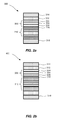
- Figure 2a illustrates a semiconductor structure device in the form of a spin-torque transfer magnetic random access memory, STT-MRAM.
- STT-MRAMs like the STT-MRAM 300, are attracting much attention because of their potential in offering a reduction of power consumption through non-volatility and a reduction of the size of memory cells compared to conventional memory cells.
- the STT-MRAM device 300 comprises a magnetic tunnel junction, MTJ, 302 providing a tunnel magneto resistance, TMR. It is further known that the MTJ may have perpendicular magnetic anisotropy, PMA such that a so called p-MTJ is formed.
- MTJ magnetic tunnel junction
- PMA perpendicular magnetic anisotropy
- the use of a p-MTJ generally offers an improved current switching and high thermal stability for the STT-MRAM device 300.
- the MTJ 302 may be formed by means of physical vapor deposition.
- the MTJ 302 consists of a stack of layers 304, 306, and 308.
- the stack of layers may, for example, comprise CoFeB, MgO, and CoFeB, respectively.
- the CoFeB layers 304 and 308 form the magnetic layers and the MgO layer 306 forms the insulating layer, also referred to as the tunnelling layer, of the MTJ 302.
- the CoFeB layer 304 is to be understood to correspond to the layer 104.
- the CoFeB layers 304 and 308 have preferentially [001] textures in order to obtain a high TMR.
- a Co/Ni perpendicular synthetic anti-ferromagnet, p-SAF, structure 310 is provided, which is arranged to pin the magnetization the CoFeB layer 308.
- the p-SAF structure 310 may also be referred to as a reference layer, RL.
- the CoFeB layer 304 is the switching element of the STT-MRAM device 300 and is commonly referred to as a free layer, FL.
- the STT-MRAM device 300 further comprises a functional metal layer 312 arranged on top of and in contact with the CoFeB layer 304.
- the functional metal layer 312 is an amorphous metal layer.
- the functional metal layer 312 comprises Ta. It should, however, be noted that the functional metal layer may in other embodiments comprise an alloy comprising Ta or be formed by Ta.
- the metal layer may moreover be a crystalline metal layer.
- the STT-MRAM device 300 may further comprise an electrode 314 formed adjacent to the functional metal layer 312.
- the electrode 314, which may be referred to as a top electrode, may comprise Ru/Ta/Ru.
- Ta may be used at various other positions within the STT-MRAM 300.
- An additional Ta layer 316 may therefore for instance be used as an amorphous interlayer to avoid texture transfer from the (111) textured FCC Co/Pt or Co/Ni based p-SAF structure 310 to the (001) textured BCC CoFeB layer 308 during a crystallization anneal.
- an additional Ta layer might be used as part of the free layer to form a CoFeB/Ta/CoFeB free layer structure.
- a semiconductor structure such as a STT-MRAM structure, may comprise an oxide layer.
- a MgO layer may for instance be used as a capping layer arranged on top of a CoFeB layer as the formed MgO/CoFeB interface may enhance the perpendicular anisotropy of the STT-MRAM structure.
- a sacrificial layer comprising for instance Mg may be used to efficiently protect the oxide layer during deposition of a functional metal layer on top of the oxide layer.
- a bottom electrical contact 318 is further arranged below the p-SAF structure 310.
- FIG. 2b illustrates a STT-MRAM 400 comprising a Co/Pt p-SAF structure 310.
- the structure of the STT-MRAM 400 is similar to the structure of the STT-MRAM 300, why its construction and function will not be described in detail in order to avoid undue repetition.
- the properties and performance of the STT-MRAMs 300, 400 depends critically of the quality of their MTJs 302, which in turn are sensitive to the quality of the functional metal layer 312.
- the depicted p-MTJ's 302, of figures 2a and 2b , on the bottom pinned p-SAF's 310 were deposited in-situ by physical vapor deposition, PVD, in a 300 mm cluster tool, EC7800 Canon-Anelva, on TaN-based bottom electrodes 318 on a substrate (not shown).
- the bottom electrodes 318 were moreover smoothened down to 0.05 nm root mean square roughness via chemical mechanical polishing, CMP prior to depositing the respective p-SAF's 310.
- the CoFeB layers 304 and 308 were also formed by PVD.
- the functional metal layers 312 of Ta were formed by use of a sacrificial metal layer (not shown) as discussed in relation to figures 1 a and 1 b.
- the sacrificial metal layers consisted in the fabrication of the STT-MRAMs 300, 400 of 0.65 nm of Mg which were deposited, by means of PVD, on top of the CoFeB layers 304.
- the CoFeB layers 304 had a thickness of 1.5 nm.
- the light Mg atoms are removed by being sputtered by the impinging Ta atoms forming the functional metal layers 312.
- a functional metal layer 312 comprising Ta is formed on the respective CoFeB layers 304.
- the deposition of the respective functional metal layers 312 resulted in a layer thickness of 1 nm.
- the substrates received a 30 minute 300°C crystallization vacuum anneal in presence of a 1 Tesla magnetic field in a TEL-MSL MRT5000 batch annealing system.
- the layers 304 and 308 may at least partially crystallize into a [001] orientated layer, which may result in an increased TMR.
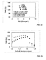
- FIG. 3a shows experimental data of measured TMR, indicated with open symbols, for the STT-MRAMs 300, and 400, i.e. STT-MRAMs comprising Ta functional layers 304 with a thickness of 1 nm which were formed by utilizing a Mg sacrificial metal layer with a thickness of 0.65 nm.
- the TMR for the STT-MRAMs 300, 400 were measured to be about 20% higher than the TMR of a reference sample comprising a functional layer of Ta deposited without utilizing a sacrificial metal layer, illustrated by solid symbols in figure 3a.
- Figure 3a also shows that for both Co/Pt p-SAF structures, square symbols, and ultrathin Co/Ni BP p-SAF structures, circle symbols, for pinning the reference layer 308 it is advantageous to use MTJs 302 comprising functional metal layers 312 which have been formed using sacrificial metal layers.
- Figure 3b further illustrates that an increase in TMR may reach 35% when the thickness of the CoFeB layer 304, i.e. the free layer, is reduced to about 1.3 nm.
- the decrease of the TMR may be attributed to the loss of perpendicular magnetic anisotropy of the CoFeB layer 304. Since the decrease occurs earlier for the functional metal layer 312 formed using a Mg sacrificial metal layer it may, erroneously, be concluded that the earlier drop of the PMA is a result of the functional metal layer 312 formed using a Mg sacrificial metal layer.
- this drop is not related to the weaker interfacial anisotropy resulting from the functional metal layer 312 formed using a Mg sacrificial metal layer.
- the earlier drop should, instead be attributed to a magnetic moment of the CoFeB layer 304 which is higher in the case of the functional metal layer 312 being formed using a Mg sacrificial metal layer indicating that a thinner dead moment is formed during Mg/Ta deposition.
- Elastic recoil detection, ERD, measurements on films comprising CoFeB layers 304 and functional metal layers 312 of Ta, where the functional metal layers 312 were formed using Ta sacrificial metal layers will be described in the following.
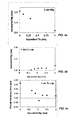
- Figure 4a illustrates the measured Mg thickness extracted from ERD measurements for films comprising 1.5 nm thick CoFeB layers and Ta functional metal layers with varying thicknesses, x.
- the respective Ta functional metal layers were deposited on a Mg sacrificial metal layer having a thickness of 2 nm.
- Figure 4a illustrates that the Mg is sputtered by about 2 nm during a 1 nm Ta deposition.
- the thickness of the sacrificial metal layer is larger than the thickness of the functional metal layer.
- the thickness of the sacrificial metal layer may for example be larger than but three times smaller than the thickness of the functional metal layer. By such an arrangement the sacrificial layer may be completely removed during the deposition of the functional metal layer.
- the etching ratio when depositing Ta on Mg is about 2, i.e. approximately 2 nm of the Mg sacrificial metal layer is etched per 1 nm deposited Ta functional metal layer.
- Figure 4b further illustrates measurements for films comprising 1.5 nm thick CoFeB layers and 1 nm thick Ta functional metal layers, where the respective functional Ta layers were deposited on Mg sacrificial metal layers of varying thicknesses, x.
- the ERD data shown in figure 4b shows that no significant amount of Mg is left on the CoFeB layers, when using sacrificial metal layers having thicknesses below 0.65 nm prior to the depositing the 1 nm Ta functional metal layer.
- the etching ratio may differ for different experimental conditions such as the processing equipment used.
- the etch rate may for example be larger such that a thickness of the sacrificial metal layer smaller than 2 nm may be used where the sacrificial layer may be completely removed during the deposition of the functional metal layer.
- Figure 4c illustrates experimental data for measurements obtained on CoFeB layers onto which sacrificial metal layers of Mg, having different thicknesses, where deposited.
- the thickness loss i.e., the reduction in thickness, of the CoFeB layers is shown as function of the thickness of the deposited sacrificial metal layer after deposition of a functional metal layer of Ta with a thickness of 1 nm.
- the dotted line shows the reference value collected on a sample without Ta deposition.
- the thickness loss data were extracted from rutherford back scattering, RBS, measurements.
- the film thickness was calculated from the ERD and RBS measurement using the bulk densities of the material involved.
- Figure 4c shows that when no Mg is present, the CoFeB layer is removed by about 0.17 nm when deposition 1 nm of Ta. It may further be concluded that for thickness up to 0.65 nm the Mg sacrificial metal layer acts as a sacrificial protective layer in the sense that the layer is completely removed. For thicker Mg sacrificial metal layers thickness a reduction of the CoFeB layer may be reduced. However, when using a thicker Mg layer portion of the Mg layer may remain on the CoFeB layer which may provide undesirable properties.
- the sacrificial metal layer was disclosed as comprising Mg and the functional metal layer as comprising Ta. This is advantageous as Mg atoms are light and the risk of damaging the top surface of the layer may therefore be reduced.
- the Ta atoms are moreover heavier than the Mg atoms such that the Ta atoms impinging on the Mg may efficiently remove the Mg.
- the sacrificial metal layer may comprise Al, Ca, Zn, or a combination thereof, which is advantageous in that the sacrificial metal layer may be removed by sputtering during the deposition of the functional metal layer.
- the risk of damaging the top surface of the layer may further be minimized as Al, Ca and Zn are also light metal elements which may be deposited with a reduced risk of damaging the top surface.
- Al, Ca and Zn efficiently protect the top surface during the deposition of the functional metal layer.
- the functional metal layer may comprise Co, Ti, W, Mo, Ru, Hf, or a combination thereof which is advantageous in that the method may be used to fabricate various types of devices comprising Co, Ti, W, Mo, Ru or Hf.
- the functional layer may, moreover, comprise these materials and Ta.
- Figure 5 illustrates experimental data for measurements obtained on CoFeB layers onto which Ta layers have been deposited.
- the dashed curve in figure 5 illustrates the measured magnetoresistance as function of annealing temperature for a layer structure where a sacrificial metal layer of Mg was used prior to the Ta deposition.
- the solid curve illustrates the measured magnetoresistance as function of annealing temperature for a layer structure where Ta was directly deposited on the CoFeB.
- the Ta capped structures fabricated by using the sacrificial layer maintain higher perpendicular anisotropy relative to the structures for which Ta was directly deposited on the CoFeB.
- the use of a sacrificial layer thereby improves the robustness during annealing and a better performance may be achieved.
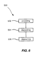
- the method 500 comprises providing 502 a layer 104 on a substrate 102, the layer 104 having an initial thickness t 0 and an initial composition C 0 , and a top surface 108.
- the sacrificial metal layer 106 deposited comprises a light metal element.
- a functional metal layer 110 is thereafter deposited 506 on and in contact with the sacrificial metal layer 106 by means of physical vapor deposition.
- the sacrificial metal layer 106 is removed by sputtering such that an interface 112 is formed between the top surface 108 and the functional metal layer 106.
- the sacrificial metal layer 106 thereby protects the top surface 108 during the deposition 506 of the functional metal layer 110 such that, the layer 104 has a final thickness t f matching the initial thickness t 0 and a final composition C f corresponding to the initial composition C 0 .
- the method 500 for protecting a top surface 108 of a layer 104 in a semiconductor structure 100, 200 may be used from other semiconductor structures than the ones disclosed above in relation to STM-MRAM devices.
- the layer 104 may for example comprise a high-k dielectric material or an oxide. More specifically, the method 500 may advantageously be used when the formation of an interface between a high-k dielectric or an oxide material and another material is crucial in the sense that the high-k dielectric or the oxide material need to be protected during the formation of other material such that the risk of damaging the high-k dielectric or the oxide material is reduced.
Landscapes
- Engineering & Computer Science (AREA)
- Chemical & Material Sciences (AREA)
- Power Engineering (AREA)
- Manufacturing & Machinery (AREA)
- Organic Chemistry (AREA)
- Metallurgy (AREA)
- Mechanical Engineering (AREA)
- Materials Engineering (AREA)
- Chemical Kinetics & Catalysis (AREA)
- Crystallography & Structural Chemistry (AREA)
- Hall/Mr Elements (AREA)
- Mram Or Spin Memory Techniques (AREA)
- Electrodes Of Semiconductors (AREA)
Abstract
Description
- The present invention relates to a method for protecting a top surface of a layer in a semiconductor structure.
- Semiconductor devices have consistently migrated to smaller feature sizes over the years, allowing more functionality to be packed in each device. This increased capacity per unit area, reduces the device footprint and costs. The downscaling is, however, not without problems. Commonly, the manufacturing of semiconductor devices involves fabrication of semiconductor structures comprising a plurality of layers. By selecting the appropriate materials each of the plurality of layers may provide a certain function within the semiconductor structure. Individual layers are generally deposited during the fabrication of the semiconductor structures so as to form for example contact layers, isolating layers or spacer layers which, respectively, allow for electrical contacting, electrical isolation or physical separation of layers.
- With smaller feature sizes devices are prone to errors such as leakage currents and charge trapping. Even variations on the nanometer scale of the material structure/composition and the interfaces between the layers may reduce device performance. The smaller feature sizes also increase the demands on the fabrication techniques used for providing the semiconductor devices.
- Physical vapor deposition, PVD, is a fabrication technique commonly used to deposit thin layers by condensation of a vaporized form of the desired layer material. The demands on PVD techniques facilitating the fabrication of layers with improved purity, thickness control as well as smoother interfaces between adjacent layers within the semiconductor structures are increasing with the downscaling.
- There is therefore a need for improved techniques for forming semiconductor structures comprising a plurality of layers.
- It is an object of the present invention to provide an improvement of the above techniques and prior art.
- According to an aspect of the invention, the above is at least partly alleviated by a method for protecting a top surface of a layer in a semiconductor structure, the method comprising: providing a layer on a substrate, the layer having an initial thickness and an initial composition, and a top surface, depositing by means of physical vapor deposition, PVD, a sacrificial metal layer on and in contact with the top surface, the sacrificial metal layer comprising a light metal element, depositing by means of physical vapor deposition a functional metal layer on and in contact with the sacrificial metal layer, whereby the sacrificial metal layer is removed by sputtering during the deposition of the functional metal layer such that an interface is formed between the top surface and the functional metal layer, the sacrificial metal layer protecting the top surface during the deposition of the functional metal layer such that, the layer has a final thickness matching the initial thickness and a final composition corresponding to the initial composition.
- The present invention is based on the realization that the use of a sacrificial metal layer may reduce damages to a layer when depositing a functional metal layer on top of the layer.
- Initially a layer is provided on a substrate. The layer may be provided directly or indirectly on the substrate. In other words, other layers or structures may be provided between the substrate and the layer. The layer provided on the substrate has an initial thickness and an initial composition. Further, the layer has a top surface. The top surface is the surface of the layer facing away from the substrate.
- A sacrificial metal layer is deposited on and in contact with the top surface by means of physical vapor deposition, PVD. In other words, a sacrificial metal layer is deposited in physical contact with the top surface. The sacrificial metal layer comprises a light metal element.
- It should be noted that within the context of this application the term "light metal element" may be any metal element having an atomic number of 36 or less. Hence, a light metal element may be any metal element in the first four periods of the periodic table.
- A functional metal layer is deposited on and in contact with the sacrificial metal layer by means of physical vapor deposition. During the deposition of the functional metal layer, the sacrificial metal layer is removed by sputtering, resulting in that an interface is formed between the top surface and the functional metal layer. The sputtering is caused by the physical vapor deposition of the functional metal layer, when the atoms forming the functional metal layer impinges on the sacrificial metal layer. The sputtering of the sacrificial metal layer involves two major mechanisms removing the atoms of the sacrificial metal layer. The first mechanism being physical sputtering of the sacrificial metal layer and the second mechanism being evaporation of the sacrificial metal layer. In order to achieve the sputtering of the sacrificial metal layer the atoms forming the functional metal layer need to transfer a sufficient impulse to the atoms of the sacrificial metal layer, as is known in the art. The impulse transferred is mainly determined by the velocity and weight of the atoms forming the functional metal layer.
- The sacrificial metal layer protects the top surface during the deposition of the functional metal layer. Hence, the atoms forming the functional metal layer will impinge on and sputter the sacrificial metal layer, such that top surface is not affected or only affected to a limited amount by the atoms forming the functional metal layer. The protective effect caused by the sacrificial metal layer results in that, the layer having the top surface has a final thickness matching the initial thickness and a final composition corresponding to the initial composition.
- It should be noted that within the context of this application the terms "final thickness" and "final composition" mean the thickness and the composition respectively after completion of the deposition of the functional metal layer. The "final thickness matching the initial thickness" is more specifically to be interpreted as the final thickness corresponds to ± 5% of the initial thickness. The "final composition corresponding to the initial composition" is more specifically to be interpreted as the final composition at least to 95% corresponds to the initial composition.
- Besides, the protective effect results in that, the intermixing of the top surface and the functional material during deposition of the functional layer is reduced.
- The layer may comprise Co, Fe, B, or a combination thereof, which is advantageous in that the method may be used with magnetic layers.
- The sacrificial metal layer may comprise Mg, Al, Ca, Zn, or a combination thereof, which is advantageous in that the sacrificial metal layer may be removed by sputtering during the deposition of the functional metal layer. Moreover, by this arrangement the risk of damaging the top surface of the layer may be minimized as Mg, Al, Ca and Zn are light metal elements which may be deposited on the top surface with a reduced risk of damaging the top surface. Further, Mg, Al, Ca and Zn efficiently protect the top surface during the deposition of the functional metal layer. Preferably Mg is used for the sacrificial metal layer.
- The functional metal layer may be an amorphous metal layer.
- The functional metal layer may comprise Ta.
- The thickness of the sacrificial metal layer may be smaller than three times the thickness of the functional metal layer. By this arrangement, the sacrificial layer may be completely removed during the deposition of the functional metal layer. For instance, when using Ta in the functional metal layer and Mg in the sacrificial metal layer, 2-3 A of Mg is removed during the deposition of 1 A Ta. In other words, the sputter yield has a factor of 2-3. A specific factor will be determined by the respective elements and system parameters used.
- A thickness of the sacrificial metal layer may be smaller than 2 nm, which is advantageous in that the sacrificial layer may be completely removed during the deposition of the functional metal layer.
- The method may further comprise, annealing the semiconductor structure at an elevated temperature of 250°C - 400°C, wherein the layer at least partially crystallizes into a [001] orientated layer, which is advantageous in that desired magnetic properties of the layer may be achieved. A [001] orientated layer may result in an increased tunnelling magneto resistance, TMR.
- The layer may have perpendicular magnetic anisotropy, which is advantageous in that the layer may exhibit desired magnetic properties.
- The layer and the functional metal layer may form part of a spin-transfer torque magnetoresistive random-access memory stack, STT-MRAM stack. By incorporating the layer and the functional metal layer in a STT-MRAM stack, an improved memory may be achieved.
- The method may further comprise, forming a magnetic tunnel junction, MTJ, by means of physical vapor deposition, wherein the layer forms part of the magnetic tunnel junction. By this arrangement, an improved memory having improved read, write and stability properties may be achieved.
- The method may further comprise forming an electrode adjacent to the functional metal layer, which is advantageous in that the electrode may be used to contact the functional metal layer and hence a device in which the functional metal layer may be incorporated.
- The layer may comprise a high-k dielectric material or an oxide. By this arrangement, the method may advantageously be used to fabricate various types of devices. More specifically, the method may advantageously be used when the formation of an interface between a high-k dielectric or an oxide material and another material is crucial in the sense that the high-k dielectric or the oxide material need to be protected during the formation of other material such that the risk of damaging the high-k dielectric or the oxide material is reduced.
- The functional metal layer may comprise Co, Ti, W, Mo, Ru, Hf, or a combination thereof which is advantageous in that the method may be used to fabricate various types of devices comprising Co, Ti, W, Mo, Ru or Hf.
- Further features of, and advantages with, the present invention will become apparent when studying the appended claims and the following description. The skilled person will realize that different features of the present invention may be combined to create embodiments other than those described in the following, without departing from the scope of the present invention.
- This and other aspects of the present invention will now be described in more detail, with reference to the enclosed drawings showing embodiments of the invention.
-
Figure 1 a illustrates a pre-stage of a semiconductor structure according to an embodiment of the present invention. -
Figures 1b illustrates a semiconductor structure according to an embodiment of the present invention. -
Figures 2a and 2b illustrates semiconductor structure devices in the form of spin-torque transfer magnetic random access memories, STT-MRAMs. -
Figures 3a and 3b illustrate measured tunnelling magnetoresistance ratios, TMR, for STT-MRAM structures as function of resistance area product, RA, and thickness. -
Figures 4a, 4b and 4c illustrate measurements for STT-MRAM structures illustrating sputtering of Mg during Ta deposition. -
Figure 5 illustrates measurements of magnetoresistance as function of annealing temperature obtained on CoFeB layers onto which Ta layers have been deposited. -
Figure 6 illustrates a method for protecting a top surface of a layer in a semiconductor structure. - The present invention will now be described more fully hereinafter with reference to the accompanying drawings, in which currently preferred embodiments of the invention are shown. This invention may, however, be embodied in many different forms and should not be construed as limited to the embodiments set forth herein. These embodiments are rather provided for thoroughness and completeness, and for fully conveying the scope of the invention to the skilled person.
- In the following a semiconductor structure and a method for protecting a top surface of a layer in the semiconductor structure will be described, with reference to
figures 1 a and 1 b. -
Figure 1 a illustrates a pre-stage of asemiconductor structure 100. The pre-stage of thesemiconductor structure 100 comprises asubstrate 102, alayer 104 and asacrificial metal layer 106. Thelayer 104 has an initial thickness, t0, and an initial composition C0, and atop surface 108. - The
sacrificial metal layer 106 is provided by deposition by means of physical vapor deposition, PVD, whereby thesacrificial metal layer 106 is formed on and in contact with thetop surface 108 of thelayer 104. Thetop surface 108 is the surface of the layer facing away from the substrate. - The
sacrificial metal layer 108 comprises, as will be further discussed below, a light metal element. -
Figure 1b illustrates asemiconductor structure 200 resulting after further processing of the pre-stage of thesemiconductor structure 100. Thesemiconductor structure 200 comprises thesubstrate 102, thelayer 104 and afunctional metal layer 110. - To form the
semiconductor structure 200 from the pre-stage of thesemiconductor 100, thefunctional metal layer 110 is provided by PVD. Thefunctional metal layer 110 is thereby deposited on and in contact with thesacrificial metal layer 106. During the depositing of thefunctional metal layer 110 thesacrificial metal layer 106 is removed by sputtering such that an interface 112 is formed between thetop surface 108 and thefunctional metal layer 110. Thesacrificial metal layer 106 thereby protects thetop surface 108 during the deposition of thefunctional metal layer 110. In other words, thesacrificial metal layer 106 thereby acts as a protecting layer, or as a cushion, reducing physical effects on thetop surface 108 during the sputtering of thefunctional metal layer 110. An improved quality of thelayer 104 is thereby achieved which is to be understood as thelayer 104 has a final thickness, tf, matching the initial thickness, t0, and a final composition, Cf, corresponding to the initial composition C0. - Atoms forming the
functional metal layer 110 will during the PVD impinge on and thereby sputter thesacrificial metal layer 106, such that thetop surface 108 is not affected or only affected to a limited amount by the atoms forming thefunctional metal layer 110. This is a result of thesacrificial metal layer 106 protecting thetop surface 108 during the deposition of thefunctional metal layer 110. Thelayer 104 having thetop surface 108 has therefore a final thickness, tf, matching the initial thickness, t0, and a final composition, Cf, corresponding to the initial composition, C0. An improved interface 112 may thereby be formed between thetop surface 108 and thefunctional metal layer 110. - The structure of
figures 1 a and 1 b may, respectively, form parts of a pre-stage of a semiconductor structure device or a semiconductor structure device.Figure 2a illustrates a semiconductor structure device in the form of a spin-torque transfer magnetic random access memory, STT-MRAM. - STT-MRAMs, like the STT-
MRAM 300, are attracting much attention because of their potential in offering a reduction of power consumption through non-volatility and a reduction of the size of memory cells compared to conventional memory cells. - The STT-
MRAM device 300 comprises a magnetic tunnel junction, MTJ, 302 providing a tunnel magneto resistance, TMR. It is further known that the MTJ may have perpendicular magnetic anisotropy, PMA such that a so called p-MTJ is formed. The use of a p-MTJ generally offers an improved current switching and high thermal stability for the STT-MRAM device 300. - The
MTJ 302 may be formed by means of physical vapor deposition. TheMTJ 302 consists of a stack oflayers MgO layer 306 forms the insulating layer, also referred to as the tunnelling layer, of theMTJ 302. - Again referring to
figures 1 a and 1 b, theCoFeB layer 304 is to be understood to correspond to thelayer 104. - The CoFeB layers 304 and 308 have preferentially [001] textures in order to obtain a high TMR. To this end, a Co/Ni perpendicular synthetic anti-ferromagnet, p-SAF,
structure 310 is provided, which is arranged to pin the magnetization theCoFeB layer 308. The p-SAF structure 310 may also be referred to as a reference layer, RL. - The
CoFeB layer 304 is the switching element of the STT-MRAM device 300 and is commonly referred to as a free layer, FL. - The STT-
MRAM device 300 further comprises afunctional metal layer 312 arranged on top of and in contact with theCoFeB layer 304. Thefunctional metal layer 312 is an amorphous metal layer. Thefunctional metal layer 312 comprises Ta. It should, however, be noted that the functional metal layer may in other embodiments comprise an alloy comprising Ta or be formed by Ta. The metal layer may moreover be a crystalline metal layer. - The STT-
MRAM device 300 may further comprise anelectrode 314 formed adjacent to thefunctional metal layer 312. - The
electrode 314, which may be referred to as a top electrode, may comprise Ru/Ta/Ru. - The skilled person in the art realizes that Ta may be used at various other positions within the STT-
MRAM 300. Anadditional Ta layer 316 may therefore for instance be used as an amorphous interlayer to avoid texture transfer from the (111) textured FCC Co/Pt or Co/Ni based p-SAF structure 310 to the (001) texturedBCC CoFeB layer 308 during a crystallization anneal. - Besides, an additional Ta layer might be used as part of the free layer to form a CoFeB/Ta/CoFeB free layer structure.
- To this end, a semiconductor structure such as a STT-MRAM structure, may comprise an oxide layer. A MgO layer may for instance be used as a capping layer arranged on top of a CoFeB layer as the formed MgO/CoFeB interface may enhance the perpendicular anisotropy of the STT-MRAM structure. The skilled person realizes that the use of a sacrificial layer comprising for instance Mg may be used to efficiently protect the oxide layer during deposition of a functional metal layer on top of the oxide layer.
- To provide efficient charge transfer in the STT-MRAM 300 a bottom
electrical contact 318 is further arranged below the p-SAF structure 310. - The skilled person in the art realizes that according to other embodiments a Co/Pt, or Co/Pd p-SAF structure may be used.
Figure 2b illustrates a STT-MRAM 400 comprising a Co/Pt p-SAF structure 310. The structure of the STT-MRAM 400 is similar to the structure of the STT-MRAM 300, why its construction and function will not be described in detail in order to avoid undue repetition. - It should be noted that the properties and performance of the STT-
MRAMs MTJs 302, which in turn are sensitive to the quality of thefunctional metal layer 312. - The depicted p-MTJ's 302, of
figures 2a and 2b , on the bottom pinned p-SAF's 310 were deposited in-situ by physical vapor deposition, PVD, in a 300 mm cluster tool, EC7800 Canon-Anelva, on TaN-basedbottom electrodes 318 on a substrate (not shown). Thebottom electrodes 318 were moreover smoothened down to 0.05 nm root mean square roughness via chemical mechanical polishing, CMP prior to depositing the respective p-SAF's 310. The CoFeB layers 304 and 308 were also formed by PVD. - The
functional metal layers 312 of Ta were formed by use of a sacrificial metal layer (not shown) as discussed in relation tofigures 1 a and 1 b. The sacrificial metal layers consisted in the fabrication of the STT-MRAMs - During this PVD deposition of Ta on Mg, the light Mg atoms are removed by being sputtered by the impinging Ta atoms forming the functional metal layers 312. As a result a
functional metal layer 312 comprising Ta is formed on the respective CoFeB layers 304. The deposition of the respectivefunctional metal layers 312 resulted in a layer thickness of 1 nm. - After the respective PVD depositions, the substrates received a 30
minute 300°C crystallization vacuum anneal in presence of a 1 Tesla magnetic field in a TEL-MSL MRT5000 batch annealing system. - By annealing the respective STT-
MRAMs layers - In the following the properties and performance of the STT-
MRAMs -
Figure 3a shows experimental data of measured TMR, indicated with open symbols, for the STT-MRAMs functional layers 304 with a thickness of 1 nm which were formed by utilizing a Mg sacrificial metal layer with a thickness of 0.65 nm. The TMR for the STT-MRAMs figure 3a. Figure 3a also shows that for both Co/Pt p-SAF structures, square symbols, and ultrathin Co/Ni BP p-SAF structures, circle symbols, for pinning thereference layer 308 it is advantageous to useMTJs 302 comprisingfunctional metal layers 312 which have been formed using sacrificial metal layers. -
Figure 3b further illustrates that an increase in TMR may reach 35% when the thickness of theCoFeB layer 304, i.e. the free layer, is reduced to about 1.3 nm. The decrease of the TMR may be attributed to the loss of perpendicular magnetic anisotropy of theCoFeB layer 304. Since the decrease occurs earlier for thefunctional metal layer 312 formed using a Mg sacrificial metal layer it may, erroneously, be concluded that the earlier drop of the PMA is a result of thefunctional metal layer 312 formed using a Mg sacrificial metal layer. However, this drop is not related to the weaker interfacial anisotropy resulting from thefunctional metal layer 312 formed using a Mg sacrificial metal layer. The earlier drop should, instead be attributed to a magnetic moment of theCoFeB layer 304 which is higher in the case of thefunctional metal layer 312 being formed using a Mg sacrificial metal layer indicating that a thinner dead moment is formed during Mg/Ta deposition. - Elastic recoil detection, ERD, measurements on films comprising CoFeB layers 304 and
functional metal layers 312 of Ta, where thefunctional metal layers 312 were formed using Ta sacrificial metal layers will be described in the following. -
Figure 4a illustrates the measured Mg thickness extracted from ERD measurements for films comprising 1.5 nm thick CoFeB layers and Ta functional metal layers with varying thicknesses, x. The respective Ta functional metal layers were deposited on a Mg sacrificial metal layer having a thickness of 2 nm.Figure 4a illustrates that the Mg is sputtered by about 2 nm during a 1 nm Ta deposition. - It may therefore be advantageous if the thickness of the sacrificial metal layer is larger than the thickness of the functional metal layer. The thickness of the sacrificial metal layer may for example be larger than but three times smaller than the thickness of the functional metal layer. By such an arrangement the sacrificial layer may be completely removed during the deposition of the functional metal layer.
- The etching ratio when depositing Ta on Mg is about 2, i.e. approximately 2 nm of the Mg sacrificial metal layer is etched per 1 nm deposited Ta functional metal layer.
-
Figure 4b further illustrates measurements for films comprising 1.5 nm thick CoFeB layers and 1 nm thick Ta functional metal layers, where the respective functional Ta layers were deposited on Mg sacrificial metal layers of varying thicknesses, x. The ERD data shown infigure 4b shows that no significant amount of Mg is left on the CoFeB layers, when using sacrificial metal layers having thicknesses below 0.65 nm prior to the depositing the 1 nm Ta functional metal layer. - The skilled person in the art realizes that the etching ratio may differ for different experimental conditions such as the processing equipment used. In other embodiments the etch rate may for example be larger such that a thickness of the sacrificial metal layer smaller than 2 nm may be used where the sacrificial layer may be completely removed during the deposition of the functional metal layer.
-
Figure 4c illustrates experimental data for measurements obtained on CoFeB layers onto which sacrificial metal layers of Mg, having different thicknesses, where deposited. The thickness loss, i.e., the reduction in thickness, of the CoFeB layers is shown as function of the thickness of the deposited sacrificial metal layer after deposition of a functional metal layer of Ta with a thickness of 1 nm. The dotted line shows the reference value collected on a sample without Ta deposition. The thickness loss data were extracted from rutherford back scattering, RBS, measurements. The film thickness was calculated from the ERD and RBS measurement using the bulk densities of the material involved. -
Figure 4c shows that when no Mg is present, the CoFeB layer is removed by about 0.17 nm whendeposition 1 nm of Ta. It may further be concluded that for thickness up to 0.65 nm the Mg sacrificial metal layer acts as a sacrificial protective layer in the sense that the layer is completely removed. For thicker Mg sacrificial metal layers thickness a reduction of the CoFeB layer may be reduced. However, when using a thicker Mg layer portion of the Mg layer may remain on the CoFeB layer which may provide undesirable properties. - In the above description the sacrificial metal layer was disclosed as comprising Mg and the functional metal layer as comprising Ta. This is advantageous as Mg atoms are light and the risk of damaging the top surface of the layer may therefore be reduced. The Ta atoms are moreover heavier than the Mg atoms such that the Ta atoms impinging on the Mg may efficiently remove the Mg.
- In other embodiments the sacrificial metal layer may comprise Al, Ca, Zn, or a combination thereof, which is advantageous in that the sacrificial metal layer may be removed by sputtering during the deposition of the functional metal layer. Moreover, by this arrangement the risk of damaging the top surface of the layer may further be minimized as Al, Ca and Zn are also light metal elements which may be deposited with a reduced risk of damaging the top surface. Further, Al, Ca and Zn efficiently protect the top surface during the deposition of the functional metal layer.
- To this end, the functional metal layer may comprise Co, Ti, W, Mo, Ru, Hf, or a combination thereof which is advantageous in that the method may be used to fabricate various types of devices comprising Co, Ti, W, Mo, Ru or Hf. The functional layer may, moreover, comprise these materials and Ta.
-
Figure 5 illustrates experimental data for measurements obtained on CoFeB layers onto which Ta layers have been deposited. The dashed curve infigure 5 illustrates the measured magnetoresistance as function of annealing temperature for a layer structure where a sacrificial metal layer of Mg was used prior to the Ta deposition. The solid curve illustrates the measured magnetoresistance as function of annealing temperature for a layer structure where Ta was directly deposited on the CoFeB. - From the experimental data it may be observed that when annealing the stacks up to 400°C, the Ta capped structures fabricated by using the sacrificial layer maintain higher perpendicular anisotropy relative to the structures for which Ta was directly deposited on the CoFeB. The use of a sacrificial layer thereby improves the robustness during annealing and a better performance may be achieved.
- In the following the method for protecting a top surface of a layer in a semiconductor structure will be discussed with reference to
figure 6 . - The
method 500 comprises providing 502 alayer 104 on asubstrate 102, thelayer 104 having an initial thickness t0 and an initial composition C0, and atop surface 108. - Next a
sacrificial metal layer 106 on and in contact with thetop surface 108, is deposited 504 by means of physical vapor deposition, PVD. Thesacrificial metal layer 106 deposited comprises a light metal element. - A
functional metal layer 110 is thereafter deposited 506 on and in contact with thesacrificial metal layer 106 by means of physical vapor deposition. During thedeposition 506 of thefunctional metal layer 110 thesacrificial metal layer 106 is removed by sputtering such that an interface 112 is formed between thetop surface 108 and thefunctional metal layer 106. Thesacrificial metal layer 106 thereby protects thetop surface 108 during thedeposition 506 of thefunctional metal layer 110 such that, thelayer 104 has a final thickness tf matching the initial thickness t0 and a final composition Cf corresponding to the initial composition C0. - The function and benefits of the
method 500 are described above in relation to the formation of thesemiconductor structures method 500 as well. In order to avoid undue repetition, reference is made to the above. - It should, however, be noted that the
method 500 for protecting atop surface 108 of alayer 104 in asemiconductor structure - The
layer 104 may for example comprise a high-k dielectric material or an oxide. More specifically, themethod 500 may advantageously be used when the formation of an interface between a high-k dielectric or an oxide material and another material is crucial in the sense that the high-k dielectric or the oxide material need to be protected during the formation of other material such that the risk of damaging the high-k dielectric or the oxide material is reduced. - The person skilled in the art further realizes that the present invention by no means is limited to the preferred embodiments described above. On the contrary, many modifications and variations are possible within the scope of the appended claims.
- Additionally, variations to the disclosed embodiments can be understood and effected by the skilled person in practicing the claimed invention, from a study of the drawings, the disclosure, and the appended claims. In the claims, the word "comprising" does not exclude other elements or steps, and the indefinite article "a" or "an" does not exclude a plurality. The mere fact that certain measures are recited in mutually different dependent claims does not indicate that a combination of these measured cannot be used to advantage.
Claims (14)
- Method (500) for protecting a top surface (108) of a layer (104, 304) in a semiconductor structure (100, 200, 300, 400), the method (500) comprising:providing (502) a layer (104, 304) on a substrate (102), the layer (104, 304) having an initial thickness (t0) and an initial composition (C0), and a top surface (108),depositing (504) by means of physical vapor deposition, PVD, a sacrificial metal layer (106) on and in contact with the top surface (108), the sacrificial metal layer (106) comprising a light metal element,depositing (506) by means of physical vapor deposition a functional metal layer (110, 312) on and in contact with the sacrificial metal layer (106), whereby the sacrificial metal layer (106) is removed by sputtering during the deposition of the functional metal layer (110, 312) such that an interface (112) is formed between the top surface (108) and the functional metal layer (110, 312), the sacrificial metal layer (106) protecting the top surface (108) during the deposition of the functional metal layer (110, 312) such that, the layer (104, 304) has a final thickness (tf) matching the initial thickness (t0) and a final composition (Cf) corresponding to the initial composition (C0).
- Method (500) according to claim 1, wherein the layer (104, 304) comprises Co, Fe, B, or a combination thereof.
- Method (500) according to any one of the preceding claims, wherein the sacrificial metal layer (106) comprises Mg, Al, Ca, Zn, or a combination thereof.
- Method (500) according to any one of the preceding claims, wherein the functional metal layer (110, 312) is an amorphous metal layer.
- Method (500) according to any one of the preceding claims, wherein the functional metal layer (110, 312) comprises Ta.
- Method (500) according to any one of the preceding claims, wherein a thickness of the sacrificial metal layer (106) is smaller than three times the thickness of the functional metal layer (110, 312).
- Method (500) according to any one of the preceding claims, wherein the thickness of the sacrificial metal layer (106) is smaller than 2 nm.
- Method (500) according to any one of the preceding claims, the method further comprising,
annealing the semiconductor structure (200) at an elevated temperature of 250°C - 400°C, wherein the layer (104, 304) at least partially crystallizes into a [001] orientated layer. - Method (500) according to any one of the preceding claims, wherein the layer (104, 304) has a perpendicular magnetic anisotropy.
- Method (500) according to any one of the preceding claims,
wherein the layer (104, 304) and the functional metal layer (110, 312) form part of a spin-transfer torque magnetoresistive random-access memory stack, STT-MRAM stack. - Method (500) according to any one of the preceding claims, the method further comprising,
forming a magnetic tunnel junction (302), MTJ, by means of physical vapor deposition, wherein the layer (104, 304) forms part of the magnetic tunnel junction (302). - Method (500) according to any one the preceding claims, the method further comprising,
forming an electrode (314) adjacent to the functional metal layer (110, 312). - Method (500) according to claim 1, wherein the layer (104, 304) comprises a high-k dielectric material or an oxide.
- Method (500) according claim 1, wherein the functional metal layer (110, 312) comprises Co, Ti, W, Mo, Ru, Hf, or a combination thereof.
Priority Applications (3)
| Application Number | Priority Date | Filing Date | Title |
|---|---|---|---|
| EP15160520.1A EP3073514B1 (en) | 2015-03-24 | 2015-03-24 | Method for protecting a top surface of a layer in a semiconductor structure |
| JP2016039882A JP6538590B2 (en) | 2015-03-24 | 2016-03-02 | Method of protecting the upper surface of a layer in a semiconductor structure |
| US15/079,407 US10333059B2 (en) | 2015-03-24 | 2016-03-24 | Method of forming a stack of layers using a sacrificial layer |
Applications Claiming Priority (1)
| Application Number | Priority Date | Filing Date | Title |
|---|---|---|---|
| EP15160520.1A EP3073514B1 (en) | 2015-03-24 | 2015-03-24 | Method for protecting a top surface of a layer in a semiconductor structure |
Publications (2)
| Publication Number | Publication Date |
|---|---|
| EP3073514A1 true EP3073514A1 (en) | 2016-09-28 |
| EP3073514B1 EP3073514B1 (en) | 2017-10-04 |
Family
ID=52736892
Family Applications (1)
| Application Number | Title | Priority Date | Filing Date |
|---|---|---|---|
| EP15160520.1A Active EP3073514B1 (en) | 2015-03-24 | 2015-03-24 | Method for protecting a top surface of a layer in a semiconductor structure |
Country Status (3)
| Country | Link |
|---|---|
| US (1) | US10333059B2 (en) |
| EP (1) | EP3073514B1 (en) |
| JP (1) | JP6538590B2 (en) |
Families Citing this family (1)
| Publication number | Priority date | Publication date | Assignee | Title |
|---|---|---|---|---|
| WO2021097756A1 (en) * | 2019-11-21 | 2021-05-27 | Texas Instruments Incorporated | Packaged electronic device with low resistance backside contact |
Citations (1)
| Publication number | Priority date | Publication date | Assignee | Title |
|---|---|---|---|---|
| US20090073737A1 (en) * | 2007-09-17 | 2009-03-19 | Ulrich Klostermann | Integrated Circuits; Methods for Manufacturing an Integrating Circuit; Memory Modules |
Family Cites Families (3)
| Publication number | Priority date | Publication date | Assignee | Title |
|---|---|---|---|---|
| US7855147B1 (en) * | 2006-06-22 | 2010-12-21 | Novellus Systems, Inc. | Methods and apparatus for engineering an interface between a diffusion barrier layer and a seed layer |
| WO2010026705A1 (en) * | 2008-09-08 | 2010-03-11 | キヤノンアネルバ株式会社 | Magnetoresistive element, method for manufacturing same, and storage medium used in the manufacturing method |
| US8558331B2 (en) * | 2009-12-08 | 2013-10-15 | Qualcomm Incorporated | Magnetic tunnel junction device |
-
2015
- 2015-03-24 EP EP15160520.1A patent/EP3073514B1/en active Active
-
2016
- 2016-03-02 JP JP2016039882A patent/JP6538590B2/en active Active
- 2016-03-24 US US15/079,407 patent/US10333059B2/en active Active
Patent Citations (1)
| Publication number | Priority date | Publication date | Assignee | Title |
|---|---|---|---|---|
| US20090073737A1 (en) * | 2007-09-17 | 2009-03-19 | Ulrich Klostermann | Integrated Circuits; Methods for Manufacturing an Integrating Circuit; Memory Modules |
Non-Patent Citations (1)
| Title |
|---|
| SWERTS J ET AL: "BEOL compatible high tunnel magneto resistance perpendicular magnetic tunnel junctions using a sacrificial Mg layer as CoFeB free layer cap", APPLIED PHYSICS LETTERS, AMERICAN INSTITUTE OF PHYSICS, US, vol. 106, no. 26, 29 June 2015 (2015-06-29), XP012198734, ISSN: 0003-6951, [retrieved on 19010101], DOI: 10.1063/1.4923420 * |
Also Published As
| Publication number | Publication date |
|---|---|
| EP3073514B1 (en) | 2017-10-04 |
| US20160284987A1 (en) | 2016-09-29 |
| JP2016181682A (en) | 2016-10-13 |
| JP6538590B2 (en) | 2019-07-03 |
| US10333059B2 (en) | 2019-06-25 |
Similar Documents
| Publication | Publication Date | Title |
|---|---|---|
| EP3264481B1 (en) | Perpendicularly magnetized ferromagnetic layers having an oxide interface allowing for improved control of oxidation | |
| JP7442580B2 (en) | Magnetic tunnel junction with tunable large perpendicular magnetic anisotropy | |
| US9082960B2 (en) | Fully compensated synthetic antiferromagnet for spintronics applications | |
| US8653614B2 (en) | Semiconductor memory device and method for manufacturing the same | |
| CN110495000B (en) | Magnetic device including perpendicular magnetization magnetic tunneling junction | |
| US8450722B2 (en) | Magnetoresistive random access memory and method of making the same | |
| CN112166509B (en) | Magnetic tunnel junction structure and method of manufacturing the same | |
| WO2019079553A1 (en) | Free layer sidewall oxidation and spacer assisted magnetic tunnel junction (mtj) etch for high performance magnetoresistive random access memory (mram) devices | |
| US11302372B2 (en) | MTJ stack containing a top magnetic pinned layer having strong perpendicular magnetic anisotropy | |
| KR102342469B1 (en) | High-temperature volatilization of sidewall materials from patterned magnetic tunnel junctions | |
| EP3073514B1 (en) | Method for protecting a top surface of a layer in a semiconductor structure | |
| US10957849B2 (en) | Magnetic tunnel junctions with coupling-pinning layer lattice matching | |
| US11329217B2 (en) | Method for manufacturing a magnetic random-access memory device using post pillar formation annealing |
Legal Events
| Date | Code | Title | Description |
|---|---|---|---|
| PUAI | Public reference made under article 153(3) epc to a published international application that has entered the european phase |
Free format text: ORIGINAL CODE: 0009012 |
|
| AK | Designated contracting states |
Kind code of ref document: A1 Designated state(s): AL AT BE BG CH CY CZ DE DK EE ES FI FR GB GR HR HU IE IS IT LI LT LU LV MC MK MT NL NO PL PT RO RS SE SI SK SM TR |
|
| AX | Request for extension of the european patent |
Extension state: BA ME |
|
| STAA | Information on the status of an ep patent application or granted ep patent |
Free format text: STATUS: REQUEST FOR EXAMINATION WAS MADE |
|
| 17P | Request for examination filed |
Effective date: 20170328 |
|
| RBV | Designated contracting states (corrected) |
Designated state(s): AL AT BE BG CH CY CZ DE DK EE ES FI FR GB GR HR HU IE IS IT LI LT LU LV MC MK MT NL NO PL PT RO RS SE SI SK SM TR |
|
| GRAP | Despatch of communication of intention to grant a patent |
Free format text: ORIGINAL CODE: EPIDOSNIGR1 |
|
| STAA | Information on the status of an ep patent application or granted ep patent |
Free format text: STATUS: GRANT OF PATENT IS INTENDED |
|
| INTG | Intention to grant announced |
Effective date: 20170516 |
|
| GRAS | Grant fee paid |
Free format text: ORIGINAL CODE: EPIDOSNIGR3 |
|
| GRAA | (expected) grant |
Free format text: ORIGINAL CODE: 0009210 |
|
| STAA | Information on the status of an ep patent application or granted ep patent |
Free format text: STATUS: THE PATENT HAS BEEN GRANTED |
|
| AK | Designated contracting states |
Kind code of ref document: B1 Designated state(s): AL AT BE BG CH CY CZ DE DK EE ES FI FR GB GR HR HU IE IS IT LI LT LU LV MC MK MT NL NO PL PT RO RS SE SI SK SM TR |
|
| REG | Reference to a national code |
Ref country code: GB Ref legal event code: FG4D |
|
| REG | Reference to a national code |
Ref country code: CH Ref legal event code: EP |
|
| REG | Reference to a national code |
Ref country code: AT Ref legal event code: REF Ref document number: 934762 Country of ref document: AT Kind code of ref document: T Effective date: 20171015 |
|
| REG | Reference to a national code |
Ref country code: IE Ref legal event code: FG4D |
|
| REG | Reference to a national code |
Ref country code: DE Ref legal event code: R096 Ref document number: 602015005077 Country of ref document: DE |
|
| REG | Reference to a national code |
Ref country code: NL Ref legal event code: MP Effective date: 20171004 |
|
| REG | Reference to a national code |
Ref country code: FR Ref legal event code: PLFP Year of fee payment: 4 |
|
| REG | Reference to a national code |
Ref country code: LT Ref legal event code: MG4D |
|
| REG | Reference to a national code |
Ref country code: AT Ref legal event code: MK05 Ref document number: 934762 Country of ref document: AT Kind code of ref document: T Effective date: 20171004 |
|
| PG25 | Lapsed in a contracting state [announced via postgrant information from national office to epo] |
Ref country code: NL Free format text: LAPSE BECAUSE OF FAILURE TO SUBMIT A TRANSLATION OF THE DESCRIPTION OR TO PAY THE FEE WITHIN THE PRESCRIBED TIME-LIMIT Effective date: 20171004 |
|
| PG25 | Lapsed in a contracting state [announced via postgrant information from national office to epo] |
Ref country code: SE Free format text: LAPSE BECAUSE OF FAILURE TO SUBMIT A TRANSLATION OF THE DESCRIPTION OR TO PAY THE FEE WITHIN THE PRESCRIBED TIME-LIMIT Effective date: 20171004 Ref country code: FI Free format text: LAPSE BECAUSE OF FAILURE TO SUBMIT A TRANSLATION OF THE DESCRIPTION OR TO PAY THE FEE WITHIN THE PRESCRIBED TIME-LIMIT Effective date: 20171004 Ref country code: NO Free format text: LAPSE BECAUSE OF FAILURE TO SUBMIT A TRANSLATION OF THE DESCRIPTION OR TO PAY THE FEE WITHIN THE PRESCRIBED TIME-LIMIT Effective date: 20180104 Ref country code: ES Free format text: LAPSE BECAUSE OF FAILURE TO SUBMIT A TRANSLATION OF THE DESCRIPTION OR TO PAY THE FEE WITHIN THE PRESCRIBED TIME-LIMIT Effective date: 20171004 Ref country code: LT Free format text: LAPSE BECAUSE OF FAILURE TO SUBMIT A TRANSLATION OF THE DESCRIPTION OR TO PAY THE FEE WITHIN THE PRESCRIBED TIME-LIMIT Effective date: 20171004 |
|
| PG25 | Lapsed in a contracting state [announced via postgrant information from national office to epo] |
Ref country code: GR Free format text: LAPSE BECAUSE OF FAILURE TO SUBMIT A TRANSLATION OF THE DESCRIPTION OR TO PAY THE FEE WITHIN THE PRESCRIBED TIME-LIMIT Effective date: 20180105 Ref country code: HR Free format text: LAPSE BECAUSE OF FAILURE TO SUBMIT A TRANSLATION OF THE DESCRIPTION OR TO PAY THE FEE WITHIN THE PRESCRIBED TIME-LIMIT Effective date: 20171004 Ref country code: BG Free format text: LAPSE BECAUSE OF FAILURE TO SUBMIT A TRANSLATION OF THE DESCRIPTION OR TO PAY THE FEE WITHIN THE PRESCRIBED TIME-LIMIT Effective date: 20180104 Ref country code: AT Free format text: LAPSE BECAUSE OF FAILURE TO SUBMIT A TRANSLATION OF THE DESCRIPTION OR TO PAY THE FEE WITHIN THE PRESCRIBED TIME-LIMIT Effective date: 20171004 Ref country code: RS Free format text: LAPSE BECAUSE OF FAILURE TO SUBMIT A TRANSLATION OF THE DESCRIPTION OR TO PAY THE FEE WITHIN THE PRESCRIBED TIME-LIMIT Effective date: 20171004 Ref country code: IS Free format text: LAPSE BECAUSE OF FAILURE TO SUBMIT A TRANSLATION OF THE DESCRIPTION OR TO PAY THE FEE WITHIN THE PRESCRIBED TIME-LIMIT Effective date: 20180204 Ref country code: LV Free format text: LAPSE BECAUSE OF FAILURE TO SUBMIT A TRANSLATION OF THE DESCRIPTION OR TO PAY THE FEE WITHIN THE PRESCRIBED TIME-LIMIT Effective date: 20171004 |
|
| REG | Reference to a national code |
Ref country code: DE Ref legal event code: R097 Ref document number: 602015005077 Country of ref document: DE |
|
| PG25 | Lapsed in a contracting state [announced via postgrant information from national office to epo] |
Ref country code: CZ Free format text: LAPSE BECAUSE OF FAILURE TO SUBMIT A TRANSLATION OF THE DESCRIPTION OR TO PAY THE FEE WITHIN THE PRESCRIBED TIME-LIMIT Effective date: 20171004 Ref country code: SK Free format text: LAPSE BECAUSE OF FAILURE TO SUBMIT A TRANSLATION OF THE DESCRIPTION OR TO PAY THE FEE WITHIN THE PRESCRIBED TIME-LIMIT Effective date: 20171004 Ref country code: DK Free format text: LAPSE BECAUSE OF FAILURE TO SUBMIT A TRANSLATION OF THE DESCRIPTION OR TO PAY THE FEE WITHIN THE PRESCRIBED TIME-LIMIT Effective date: 20171004 Ref country code: EE Free format text: LAPSE BECAUSE OF FAILURE TO SUBMIT A TRANSLATION OF THE DESCRIPTION OR TO PAY THE FEE WITHIN THE PRESCRIBED TIME-LIMIT Effective date: 20171004 |
|
| PLBE | No opposition filed within time limit |
Free format text: ORIGINAL CODE: 0009261 |
|
| STAA | Information on the status of an ep patent application or granted ep patent |
Free format text: STATUS: NO OPPOSITION FILED WITHIN TIME LIMIT |
|
| PG25 | Lapsed in a contracting state [announced via postgrant information from national office to epo] |
Ref country code: RO Free format text: LAPSE BECAUSE OF FAILURE TO SUBMIT A TRANSLATION OF THE DESCRIPTION OR TO PAY THE FEE WITHIN THE PRESCRIBED TIME-LIMIT Effective date: 20171004 Ref country code: IT Free format text: LAPSE BECAUSE OF FAILURE TO SUBMIT A TRANSLATION OF THE DESCRIPTION OR TO PAY THE FEE WITHIN THE PRESCRIBED TIME-LIMIT Effective date: 20171004 Ref country code: PL Free format text: LAPSE BECAUSE OF FAILURE TO SUBMIT A TRANSLATION OF THE DESCRIPTION OR TO PAY THE FEE WITHIN THE PRESCRIBED TIME-LIMIT Effective date: 20171004 Ref country code: SM Free format text: LAPSE BECAUSE OF FAILURE TO SUBMIT A TRANSLATION OF THE DESCRIPTION OR TO PAY THE FEE WITHIN THE PRESCRIBED TIME-LIMIT Effective date: 20171004 |
|
| 26N | No opposition filed |
Effective date: 20180705 |
|
| REG | Reference to a national code |
Ref country code: CH Ref legal event code: PL |
|
| PG25 | Lapsed in a contracting state [announced via postgrant information from national office to epo] |
Ref country code: MC Free format text: LAPSE BECAUSE OF FAILURE TO SUBMIT A TRANSLATION OF THE DESCRIPTION OR TO PAY THE FEE WITHIN THE PRESCRIBED TIME-LIMIT Effective date: 20171004 Ref country code: SI Free format text: LAPSE BECAUSE OF FAILURE TO SUBMIT A TRANSLATION OF THE DESCRIPTION OR TO PAY THE FEE WITHIN THE PRESCRIBED TIME-LIMIT Effective date: 20171004 |
|
| REG | Reference to a national code |
Ref country code: BE Ref legal event code: MM Effective date: 20180331 |
|
| REG | Reference to a national code |
Ref country code: IE Ref legal event code: MM4A |
|
| PG25 | Lapsed in a contracting state [announced via postgrant information from national office to epo] |
Ref country code: LU Free format text: LAPSE BECAUSE OF NON-PAYMENT OF DUE FEES Effective date: 20180324 |
|
| PG25 | Lapsed in a contracting state [announced via postgrant information from national office to epo] |
Ref country code: IE Free format text: LAPSE BECAUSE OF NON-PAYMENT OF DUE FEES Effective date: 20180324 |
|
| PG25 | Lapsed in a contracting state [announced via postgrant information from national office to epo] |
Ref country code: BE Free format text: LAPSE BECAUSE OF NON-PAYMENT OF DUE FEES Effective date: 20180331 Ref country code: CH Free format text: LAPSE BECAUSE OF NON-PAYMENT OF DUE FEES Effective date: 20180331 Ref country code: LI Free format text: LAPSE BECAUSE OF NON-PAYMENT OF DUE FEES Effective date: 20180331 |
|
| GBPC | Gb: european patent ceased through non-payment of renewal fee |
Effective date: 20190324 |
|
| PG25 | Lapsed in a contracting state [announced via postgrant information from national office to epo] |
Ref country code: GB Free format text: LAPSE BECAUSE OF NON-PAYMENT OF DUE FEES Effective date: 20190324 Ref country code: MT Free format text: LAPSE BECAUSE OF NON-PAYMENT OF DUE FEES Effective date: 20180324 |
|
| PG25 | Lapsed in a contracting state [announced via postgrant information from national office to epo] |
Ref country code: TR Free format text: LAPSE BECAUSE OF FAILURE TO SUBMIT A TRANSLATION OF THE DESCRIPTION OR TO PAY THE FEE WITHIN THE PRESCRIBED TIME-LIMIT Effective date: 20171004 |
|
| PG25 | Lapsed in a contracting state [announced via postgrant information from national office to epo] |
Ref country code: PT Free format text: LAPSE BECAUSE OF FAILURE TO SUBMIT A TRANSLATION OF THE DESCRIPTION OR TO PAY THE FEE WITHIN THE PRESCRIBED TIME-LIMIT Effective date: 20171004 |
|
| PG25 | Lapsed in a contracting state [announced via postgrant information from national office to epo] |
Ref country code: MK Free format text: LAPSE BECAUSE OF NON-PAYMENT OF DUE FEES Effective date: 20171004 Ref country code: HU Free format text: LAPSE BECAUSE OF FAILURE TO SUBMIT A TRANSLATION OF THE DESCRIPTION OR TO PAY THE FEE WITHIN THE PRESCRIBED TIME-LIMIT; INVALID AB INITIO Effective date: 20150324 Ref country code: CY Free format text: LAPSE BECAUSE OF FAILURE TO SUBMIT A TRANSLATION OF THE DESCRIPTION OR TO PAY THE FEE WITHIN THE PRESCRIBED TIME-LIMIT Effective date: 20171004 |
|
| PG25 | Lapsed in a contracting state [announced via postgrant information from national office to epo] |
Ref country code: AL Free format text: LAPSE BECAUSE OF FAILURE TO SUBMIT A TRANSLATION OF THE DESCRIPTION OR TO PAY THE FEE WITHIN THE PRESCRIBED TIME-LIMIT Effective date: 20171004 |
|
| P01 | Opt-out of the competence of the unified patent court (upc) registered |
Effective date: 20230513 |
|
| REG | Reference to a national code |
Ref country code: DE Ref legal event code: R079 Ref document number: 602015005077 Country of ref document: DE Free format text: PREVIOUS MAIN CLASS: H01L0021285000 Ipc: H10D0064010000 |
|
| PGFP | Annual fee paid to national office [announced via postgrant information from national office to epo] |
Ref country code: DE Payment date: 20260219 Year of fee payment: 12 |
|
| PGFP | Annual fee paid to national office [announced via postgrant information from national office to epo] |
Ref country code: FR Payment date: 20260219 Year of fee payment: 12 |