EP3073412A1 - Data processing system with temperature monitoring for security - Google Patents
Data processing system with temperature monitoring for security Download PDFInfo
- Publication number
- EP3073412A1 EP3073412A1 EP16161724.6A EP16161724A EP3073412A1 EP 3073412 A1 EP3073412 A1 EP 3073412A1 EP 16161724 A EP16161724 A EP 16161724A EP 3073412 A1 EP3073412 A1 EP 3073412A1
- Authority
- EP
- European Patent Office
- Prior art keywords
- temperature
- trim value
- value
- processing system
- trim
- Prior art date
- Legal status (The legal status is an assumption and is not a legal conclusion. Google has not performed a legal analysis and makes no representation as to the accuracy of the status listed.)
- Granted
Links
Images

Classifications
-
- G—PHYSICS
- G06—COMPUTING OR CALCULATING; COUNTING
- G06F—ELECTRIC DIGITAL DATA PROCESSING
- G06F21/00—Security arrangements for protecting computers, components thereof, programs or data against unauthorised activity
- G06F21/70—Protecting specific internal or peripheral components, in which the protection of a component leads to protection of the entire computer
- G06F21/86—Secure or tamper-resistant housings
-
- G—PHYSICS
- G01—MEASURING; TESTING
- G01K—MEASURING TEMPERATURE; MEASURING QUANTITY OF HEAT; THERMALLY-SENSITIVE ELEMENTS NOT OTHERWISE PROVIDED FOR
- G01K3/00—Thermometers giving results other than momentary value of temperature
- G01K3/005—Circuits arrangements for indicating a predetermined temperature
-
- G—PHYSICS
- G01—MEASURING; TESTING
- G01R—MEASURING ELECTRIC VARIABLES; MEASURING MAGNETIC VARIABLES
- G01R31/00—Arrangements for testing electric properties; Arrangements for locating electric faults; Arrangements for electrical testing characterised by what is being tested not provided for elsewhere
- G01R31/28—Testing of electronic circuits, e.g. by signal tracer
- G01R31/317—Testing of digital circuits
- G01R31/31719—Security aspects, e.g. preventing unauthorised access during test
-
- G—PHYSICS
- G06—COMPUTING OR CALCULATING; COUNTING
- G06F—ELECTRIC DIGITAL DATA PROCESSING
- G06F21/00—Security arrangements for protecting computers, components thereof, programs or data against unauthorised activity
- G06F21/70—Protecting specific internal or peripheral components, in which the protection of a component leads to protection of the entire computer
- G06F21/71—Protecting specific internal or peripheral components, in which the protection of a component leads to protection of the entire computer to assure secure computing or processing of information
-
- G—PHYSICS
- G06—COMPUTING OR CALCULATING; COUNTING
- G06F—ELECTRIC DIGITAL DATA PROCESSING
- G06F21/00—Security arrangements for protecting computers, components thereof, programs or data against unauthorised activity
- G06F21/70—Protecting specific internal or peripheral components, in which the protection of a component leads to protection of the entire computer
- G06F21/71—Protecting specific internal or peripheral components, in which the protection of a component leads to protection of the entire computer to assure secure computing or processing of information
- G06F21/75—Protecting specific internal or peripheral components, in which the protection of a component leads to protection of the entire computer to assure secure computing or processing of information by inhibiting the analysis of circuitry or operation
- G06F21/755—Protecting specific internal or peripheral components, in which the protection of a component leads to protection of the entire computer to assure secure computing or processing of information by inhibiting the analysis of circuitry or operation with measures against power attack
-
- G—PHYSICS
- G06—COMPUTING OR CALCULATING; COUNTING
- G06F—ELECTRIC DIGITAL DATA PROCESSING
- G06F21/00—Security arrangements for protecting computers, components thereof, programs or data against unauthorised activity
- G06F21/70—Protecting specific internal or peripheral components, in which the protection of a component leads to protection of the entire computer
- G06F21/81—Protecting specific internal or peripheral components, in which the protection of a component leads to protection of the entire computer by operating on the power supply, e.g. enabling or disabling power-on, sleep or resume operations
Definitions
- This disclosure relates generally to data processing systems, and more specifically, to data processing systems with temperature monitoring for security.
- SoC System on Chip
- SoCs may include temperature monitors which indicate when a temperature of the SoC has reached a temperature outside of the specified temperature range. If the temperature has reached a lower or higher temperature than the specified range, a signal is generated which may be used to indicate that the SoC was possibly hacked.
- the temperature ranges provided by a manufacturer are typically fixed and they may therefore not be suitable for a customer's needs. If the ranges are incorrect, the signal may not provide an effective way to indicate a possible hacking of the SoC. For example, the signal may provide too many false positives. Therefore, a need exists for improved temperature-based tamper detection.
- a processing system includes a processor, and a temperature security module coupled to provide a temperature tamper signal to the processor.
- the temperature security module includes a shelf mode trim value; an operating mode trim value; and a programmable temperature trim value, wherein one of a group consisting of: the programmable temperature trim value, the shelf mode trim value, and the operating mode trim value, is used based on a deployment mode of the processing system to set a temperature monitor trim value.
- the temperature security module further includes trim select logic configured to select between the shelf mode trim value and the operating mode trim value.
- the processing system further includes a programmable temperature trim select indicator configured to select between the programmable temperature trim value, and one of the shelf mode trim value and the operating mode trim value selected by the trim select logic.
- a first value of the deployment mode indicates the processing system has not left a manufacturer of the processing system
- a second value of the deployment mode indicates the processing system has been integrated in a product
- a battery power supply is provided to the temperature security module
- secure information has been programmed in the processing system
- operating power is not provided to the processing system
- a shelf mode indicator indicates shelf mode
- a third value of the deployment mode indicates the processing system has been placed in use by the customer and the shelf mode indicator does not indicate shelf mode.
- the shelf mode trim value includes a high shelf mode trim value and a low shelf mode trim value
- the operating mode trim value includes a high operating mode trim value and a low operating mode trim value
- the programmable temperature trim value includes a high programmable temperature trim value and a low programmable temperature trim value.
- the temperature security module further includes a low temperature offset value that is used to adjust a selected one of the low shelf mode trim value, the low operating mode trim value, and the low programmable temperature trim value, and a high temperature offset value that is used to adjust a selected one of the high shelf mode trim value, the high operating mode trim value, and the high programmable temperature trim value.
- the temperature security module further includes a programmable trim disable indicator to prevent use of the programmable temperature trim value; a one-time programmable trim value lock indicator to lock the programmable temperature trim value and prevent any changes to the programmable temperature trim value until battery power is removed and applied again to the temperature security module.
- the temperature security module further includes a temperature monitor configured to provide the temperature tamper signal when a detected temperature of the processing system is not within a temperature range indicated by the selected one of the programmable temperature trim value, the shelf mode trim value, and the operating mode trim value.
- the shelf mode trim value, the operating mode trim value, and the programmable temperature trim value are different from one another.
- the temperature security module operates on battery power and the battery power is supplied to the temperature security module even when a supply power is not provided to the processor.
- the processing system further includes a security controller, wherein the security controller prevents access to the secure information in the processing system when the deployment mode has the second value.
- a processing system in another embodiment, includes secure storage circuitry; a security controller; a temperature security module coupled to provide a temperature tamper signal to the security controller; a battery power supply coupled to supply power to the secure storage circuitry, the security controller, and the temperature security module.
- the temperature security module is configured to select between a shelf mode temperature trim value, an operating mode temperature trim value, and a programmable temperature trim value based on whether a shelf mode indicator indicates the processing system is in shelf mode.
- the secure storage circuitry prevents access to secure information in the secure storage circuitry when the shelf mode indicator indicates the processing system is in the shelf mode.
- the temperature security module further includes a temperature monitor configured to provide the temperature tamper signal when a detected temperature of the processing system is not within a temperature range indicated by a selected one of the programmable temperature trim value, the shelf mode trim value, and the operating mode trim value.
- the shelf mode trim value includes a high shelf mode trim value and a low shelf mode trim value
- the operating mode trim value includes a high operating mode trim value and a low operating mode trim value
- the programmable temperature trim value includes a high programmable temperature trim value and a low programmable temperature trim value.
- the temperature security module further includes a low temperature offset value that is used to adjust a selected one of the low shelf mode trim value, the low operating mode trim value, and the low programmable temperature trim value, and a high temperature offset value that is used to adjust a selected one of the high shelf mode trim value, the high operating mode trim value, and the high programmable temperature trim value.
- the temperature security module selects the shelf mode temperature trim value when operating power supply is not provided to the processing system and the shelf mode indicator indicates the shelf mode.
- a method in yet another embodiment, includes providing a processing system on a chip (SOC), wherein the SOC includes a processor and a temperature security module coupled to provide a temperature tamper signal to the processor; configuring the temperature security module to select one of a group consisting of: a shelf mode trim value when the processing system is in shelf mode, an operating mode trim value when the processing system is in operating mode, and a programmable temperature trim value to override a selected one of the shelf mode trim value and the operating mode trim value.
- SOC processing system on a chip
- the method further includes configuring the temperature security module to disable use of the programmable temperature trim value when the shelf mode trim value is within an expected operating temperature range; and prevent any changes to the programmable temperature trim value until battery power is removed and re-applied to the temperature security module.
- the method further includes configuring the temperature security module to use at least one of a group consisting of a low temperature offset and a high temperature offset to adjust a selected one of the shelf mode trim value, the operating mode trim value, and the programmable temperature trim value.
- a temperature security module of an SoC is capable of operating in a normal operating mode and in a shelf mode.
- An SoC manufacturer programs an operating mode trim value into the temperature security module which indicates a valid temperature range during operating mode. During operating mode, if a temperature of the SoC goes beyond the valid temperature range, the temperature security module asserts a temperate tamper signal.
- the customer receives an SoC from a manufacturer, the customer is able to determine whether the operating mode trim value provided by the manufacturer meets the requirements needed by the customer for appropriately asserting a temperature tamper signal. In some cases, a customer may require a trim value which further restricts a valid temperature range of the SoC provided by the manufacturer. Therefore, in one embodiment, programmable elements are provided which allow a customer to override the values provided by the manufacturer.
- the SoC manufacturer also programs a shelf mode trim value into the temperature security module which is used to indicate a temperature range during shelf mode which is greater than the valid temperature range during operating mode.
- shelf mode behavior of the temperature tamper signal is modified to allow the SoC to be initially exposed to extreme temperatures outside the valid temperature range without resulting in assertion of the temperature tamper signal.
- operating mode is enabled and shelf mode is permanently disabled.
- shelf mode the temperature of the SoC can no longer go beyond the valid temperature range without resulting in assertion of the temperature tamper signal. In this manner, customers may be provided with improved flexibility and yield while still maintaining appropriate levels of temperature-based security.
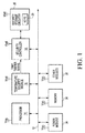
- FIG. 1 illustrates, in block diagram form, a data processing system 10 in accordance with one embodiment of the present invention.
- System 10 may be an SoC in which all modules are located on a same integrated circuit die.
- System 10 includes a processor 14, an interconnect 12, a power module 24, a memory 26, other modules 28, a temperature security module 16, a security controller 18, and secure storage circuitry 20.
- Secure storage circuitry 20 is configured to store sensitive information such as, for example, one or more keys 22.
- Processor 14, temperature security module 16, security controller 18, power module 24, memory 26, and other modules 28 may each be bidirectionally coupled to interconnect 12.
- Processor 14, power module 24, memory 26, and other modules 28 include an internal power supply node which is coupled to receive a first power supply voltage, Vdd. This power supply voltage may be provided, for example, by power module 24.
- Temperature security module 16 provides a temperature tamper signal to security controller 18.
- System 10 may be an SoC which can be used for any type of product or device.
- System 10 operates in a variety of deployment modes throughout its lifetime. Initially, system 10 is manufactured by a manufacturer. Therefore, a first deployment mode indicates that system 10 has not yet left the manufacturer. After manufacture, it is sent to a customer which may integrate the SoC into a larger system or product. The customer may program secure information into system 10, such as into secure storage circuitry 20. Furthermore, as will be described in more detail below, trim values may be programmed into temperature security module 16. After the programming of the secure information and trim values, operating power is no longer provided to system 10 and a battery, such as a coin battery, supplies power (Vbatt) to temperature security module 16, security controller 18, and secure storage circuitry 20.
- Vbatt voltage regulator
- a second deployment mode This is referred to as a second deployment mode.
- the final product may then be deployed by the customer to the field.
- Deployment to the field includes transportation and storage of the product which includes system 10.
- a third deployment mode indicates that system 10 is in use in the field. Until system 10 is in use in the field, system 10 may be considered to be in a "shelf mode" and upon entering the field, system 10 is placed in "operating mode” in which system 10 is no longer in shelf mode.
- temperature security module 16 monitors the temperature of system 10 to determine when the temperature has gone beyond a valid temperature range. If temperature security module 16 determines that the temperature of system 10 has gone below a lower bound of the valid temperature range or above an upper bound of the valid temperature range, temperature security module 16 asserts the temp tamper signal to indicate that the temperature of system 10 has gone beyond the acceptable temperature range which provides a warning that system 10 may have been hacked or been vulnerable to being hacked. In response to assertion of the temp tamper signal, security controller 18 may take appropriate action, such as clear keys 22 and any other information stored within secure storage circuitry 20.
- system 10 Prior to use of system 10 in the field, though, such as during shipping or being stored prior to use in the field, system 10 may be exposed to extreme temperatures which would typically result in assertion of the temp tamper signal. Therefore, prior to use in the field, system 10 may be maintained in a shelf mode. While in shelf mode, system 10 is in a low power mode in which system 10 is only powered by a battery, such as a coin battery. In the illustrated example, only temperature security module 16, security controller 18, and secure storage circuitry 20 within the battery domain are powered during the low power mode. Furthermore, during shelf mode, a temperature range larger than the valid temperature range is used in determining whether or not to assert the temp tamper signal. When system 10 is deployed for use in the field, shelf mode is disabled so that system 10 enters the normal operating mode in which the valid temperature range is used. In order to maintain security, once shelf mode is disabled, it cannot again be reenabled.
- security controller 18 may receive other security related signals, aside from temperature monitoring, from within system 10 and take similar action when a hacking is possible. For example, voltage and currents may be monitored by other modules within system 10 and provide information to security controller 18 accordingly.
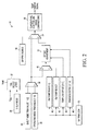
- FIG. 2 illustrates in block diagram form a portion of temperature security module 16.
- Temperature security module 16 includes storage circuitry configured to store a shelf mode trim value 34, an operating mode trim value 36, a shelf mode indicator 30, a software temperature trim value 40 (also referred to as a programmable temperature trim value), a software select value 42, a temperature low offset value 44, a temperature high offset value 46, a software trim disable indicator 50, and a software trim lock 51.
- Temperature security module 16 also includes multiplexers (MUXes) 38, 48, and 54, trim select logic 32, offset adjustment logic 52, and a temperature monitor and range comparators 56. Trim select logic 32, offset adjustment 52, and temperature monitor and range comparators are coupled to the battery power supply node to receive Vbatt.
- MUXes multiplexers
- Trim select logic is coupled to the Vdd power supply node and coupled to receive shelf mode indicator 30.
- a first data input of MUX 38 is coupled to receive shelf mode trim value 34, a second data input of MUX 38 is coupled to receive operating mode trim value 36, and a control input of MUX 38 is coupled to an output of trim select logic 32.
- a first data input of MUX 48 is coupled to an output of MUX 38, a second data input of MUX 48 is coupled to receive SW temp trim value 40, and a control input of MUX 48 is coupled to SW temp select 42.
- Offset adjustment 52 is coupled to an output of MUX 48, and is coupled to receive temp low offset value 44 and temp high offset value 46.
- a first data input of MUX 54 is coupled to the output of MUX 38, a second data input of MUX 54 is coupled to an output of offset adjustment 52, and a control input of MUX 54 is coupled to SW trim disable indicator 50.
- Temperature monitor and range comparators 56 is coupled to an output of MUX 54 and provides a temperature tamper signal (also referred to as the temp tamper signal).
- shelf mode indicator 30 is a one time programmable element, such as a fuse, in which initially (e.g. prior to programming the fuse) shelf mode indicator 30 is unprogrammed and indicates shelf mode is enabled.
- shelf mode trim value 34, operating mode trim value 36, and SW trim disable value 50 are one time programmable elements, such as fuses.
- SW temp trim value 40, SW temp select value 42, temp low offset value 44, temp high offset value 46, and SW trim lock 51 are one time programmable until power on reset (POR) elements. That is, they can only be written once after each POR, unlike a one time programmable element which can only be written once ever.
- POR power on reset
- each of these programmable until POR elements are defaulted to a logic level zero upon a POR. Furthermore, since these elements are within the battery power domain of Vbatt, the battery needs to be removed and re-applied to allow these elements to be programmed again.
- temperature monitor and range comparators 56 monitor a temperature of system 10 to determine whether the temperature has fallen outside the valid temperature range. Comparators within temperature monitor and range comparators 56 receive a temperature of system 10 from the temperature monitor and compare the results to references provided by a reference generator, such as a bandgap reference generator. The references are therefore used to provide an upper and lower bound of a temperature range. If a comparator determines that the temperature falls beyond an upper bound or lower bound provided by the references, the temp tamper signal is asserted, indicating that the temperature has fallen below or risen above a valid temperature range in which safe operation can be guaranteed. Assertion of the temp tamper signal may be in indication that SoC 10 has been hacked.
- Operation of the temperature monitor and comparators of temperature monitor and range comparators 56 may be adjusted through the use of trim values.
- a trim value is provided from the output of MUX 54 to temperature monitor and range comparators 56. The trim value is determined based on the control inputs to MUXes 38, 48, and 54. The trim value, prior to being provided to temperature monitor and range comparators 56, may also be adjusted by offset adjustment 52.
- shelf mode indicator 30, prior to being programmed defaults to indicate that shelf mode is enabled for system 10. If shelf mode indicator 30 indicates shelf mode is enabled and no power is detected at the Vdd power supply node, trim select logic 32 selects the first input of MUX 38 such that shelf mode trim value 34 is provided as the output of MUX 38.
- shelf mode trim value 34 is provided via MUX 48, offset adjustment 52, and MUX 54 to temperature monitor and range comparators 56. Offset adjustment 52 does not modify shelf mode trim value 34 since offsets 44 and 46 are zero.
- trim select logic 32 selects the second input of MUX 38 such that operating mode trim value 36 is provided as the output of MUX 38.
- shelf mode indicator 30 is programmed to disable shelf mode. For example, the fuse can be programmed to disable shelf mode. Upon shelf mode being disabled, system 10 enters operating mode.
- trim select logic 32 selects the second input of MUX 38 such that operating mode trim value 36 is provided as the output of MUX 38.
- either operating mode trim value 36 or SW temp trim value 40 is provided as the output of MUX 48 to offset adjustment 52.
- Offset adjustment 52 uses offset values 44 and 46 to adjust the received trim value (one of operating trim value 36 or SW temp trim value 40) and provides the resulting trim value to the second input of MUX 54. If SW trim is not disabled (if SW trim disable 50 is a logic level zero), the resulting trim value is provided to temperature monitor and range comparators 56.
- operating mode trim value 36 is provided, via the first input of MUX 54, to temperature monitor and range comparators 56. Operation of temperature security module 18 will be described in more detail in reference to the temperature ranges of FIG. 3 .
- FIG. 3 illustrates various temperature ranges for system 10.
- An SoC manufacturer typically guarantees proper operation in a valid operating range, such as field operating range 66 between temperatures T4 and T5.
- T4 may be -20 degrees Celsius and T5 may be 120 degrees Celsius. Any temperature of SoC 10 which falls within range 66 between T4 and T5 is considered safe and the temp tamper signal is not asserted.
- the temp tamper signal is asserted.
- T2 may be -40 degrees Celsius and T7 may be 140 degrees Celsius.
- the temp tamper signal is asserted when the temperature of SoC falls below a particular temperature between T2 and T4 of low temp range 62 or rises above a particular temperature between T5 and T7 of high temp range 70.
- the particular temperature in range 62 or in range 70 which results in assertion of the temp tamper signal corresponds to a comparator trip point of temperature monitor and range comparators 56.
- ranges 62 and 70 provide a level of uncertainty as to at which temperature within each range the temp tamper signal will be asserted. It is desirable to make these distributions as tight as possible, thus reducing ranges 62 and 70, which reduces the range of uncertainty as to the temperature between T2 and T4 and the temperature between T5 and T7 which will result in assertion of the temp temper signal.
- trim values for temperature monitor and range comparators 56 which can counter the effects of process variation and thus reduce the width of ranges 62 and 70 as much as possible.
- the trim values should be chosen such that T4 is equal to T2 and T5 equal to T7, or that they are at least as close as possible to each other. The closer T4 is to T2 and the closer T5 is to T7, the higher the accuracy provided by temperature monitor and range comparators 56 and the greater the width of field operating range 66 in which the temp tamper signal will not be asserted. It is desirable to make the width of range 66 as great as possible within SoC operation range 68 so that a manufacturer can guarantee proper operation to a customer over a larger temperature range.
- These trim values can be programmed by the manufacturer on each SoC to allow for the greatest valid temperature range of the device. These trim values correspond to operating mode trim value 36 in system 10 of FIG. 2 .
- operating mode trim value 36 includes a low operating mode trim value and a high operating mode trim value.
- operating mode trim value 36 may be a 12 bit value in which 6 bits affect the comparison at the low end of field operating range 66 and 6 bits affect the comparison at the high end of field operating range 66. That is, 6 bits result in reducing the width of range 62 by moving T4 closer to T2 and the other 6 bits result in reducing the width of range 70 by moving T5 closer to T7.
- a customer of system 10 may wish to change or restrict the temperature boundaries provided by the manufacturer of system 10. For example, for operating mode, a customer may wish to provide a smaller valid temperature range than provided by operating mode trim value 36.
- a customer may program its own trim value corresponding to each of the high end and low end of field operating range 66.
- the customer based on its own testing and evaluation, may program a software temperature trim value 40 into system 10 and then program SW temp select 42 to a logic level 1 so as to allow MUX 48 to select SW temp trim value 40 rather than operating mode trim value 36.
- SW temp trim value 40 may represent the customer's attempt to cancel out process variations and tighten the Gaussian distributions of ranges 62 and 70.
- SW temp trim value 40 may include a high SW temp trim value and a low SW temp trim value. For example, it may be a 12 bit value in which 6 bits affect the comparison at the low end of field operating range 66 and 6 bits affect the comparison at the high end of field operating range 66.
- each offset value may be a 2-bit value in which each of the 4 possible 2-bit combinations corresponds to a particular temperature offset. For example, 0b00 may correspond to no change to the trim value, 0b01 may correspond to an addition of a first predetermined amount to the trim value, 0b10 may correspond to an addition of a second predetermined amount greater than the first amount to the trim value, and 0b11 may correspond to a subtraction of a predetermined amount from the trim value.
- adjustment of the trim values with the offsets corresponds to shifting the center point of the Gaussian distributions of ranges 62 and 70.
- temp low offset 44 may be used to modify the 6 bits which affect the comparison at the low end of range 66
- high temp offset 46 may be used to modify the 6 bits which affect the comparison at the high end of range 66.
- the offset values may only be used to further restrict the valid temperature range. Therefore, a customer has the option to override trim values programmed into one time programmable memory by the manufacturer through the use of SW trim value 40, and offsets 44 and 46.
- a customer may decide not to override operating mode trim value 36 and may therefore assert SW trim disable 50 by, for example, programming a fuse.
- operating mode trim value 36 is provided to temperature monitor and range comparators 56 without any modification by way of MUXes 38 and 54. That is, with SW trim disable indicator 50 asserted, SW temp trim value 40, SW temp select 42, and offsets 44 and 46 do not affect operating mode trim value 36 being provided to temperature monitor and range comparators 56.
- the software trim values can be locked or disabled to prevent updates to any of SW temp trim value 40, SW temp select 42, and offsets 44 and 46.
- SW trim lock 51 initially defaults to being negated (e.g.
- SW trim lock 51 may be written to once after reset, in which, once asserted (e.g. written to a second logic state), changes to any of these values is prevented.
- the lock indicator Upon removal and reapplication of the battery which provides Vbatt, the lock indicator is defaulted back to being negated, thus again allowing changes to the SW temp trim value.
- system 10 may be subjected to temperatures outside of range 68 in which the temperature falls below T2 or above T7.
- temperatures may reach values outside of range 68. Therefore, system 10 is initially placed in shelf mode in which system 10 operates in a low power mode using Vbatt, as discussed above, and temperatures are allowed to fall outside of SoC operating range 68 without triggering assertion of the temp tamper signal.
- the manufacturer may therefore also program a shelf mode trim value into the SoC, such as shelf mode trim value 34 of FIG. 2 , which are used by temperature monitor and range comparators 56 prior to exiting shelf mode. Shelf mode trim value 34 is provided to temperature monitor and range comparators 56 via MUXes 38 and 48 if SW trim disable 50 is a logic level 0 or via MUXes 38 and 54 if SW trim disable 50 is a logic level 1.
- shelf mode trim value 34 includes a low shelf mode trim value and a high shelf mode trim value.
- shelf mode trim value 34 may be a 6 bit value in which 6 bits affect the comparison at the lower temperature and 6 bits affect the comparison at the higher temperatures.
- the shelf mode trim value shifts the comparator trip points within temperature monitor and comparators 56 to T2 and T7. In this manner, when in shelf mode and the temperature of the SoC falls into range 60 between T1 and T2 or falls into range 74 between T7 and T8, the temp tamper signal is not asserted as it would be if system 10 were not in shelf mode.
- the range of temperatures which do not result in assertion of the temp tamper signal (T1 to T8) is larger than SoC operating range 68.
- the temp tamper signal upon disabling shelf mode, the temp tamper signal will be asserted at a particular temperature within range 60 or 74.
- trim values provided to temperature monitor and range comparators 56 may affect the temperature ranges in a variety of different ways.
- the trim values can adjust the reference input of the range comparator against which the temperature value from the temperature monitor is compared.
- the trim values may be used in different ways to indicate the temperature ranges used to generate the temp tamper signal.
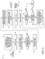
- FIG. 4 illustrates a method 76 for adjusting temperature ranges in accordance with one embodiment of the present invention.
- Method 76 begins with block 78 in which a manufacturer of a system, such as an SoC, determines and sets shelf mode trim values and operating mode trim values for a temperature security module of an SoC.
- Block 78 may correspond to the first deployment mode of the system.
- the manufacturer then ships the system to a customer.
- Method proceeds to block 80 in which the customer powers up the SoC.
- the one time programmable upon reset elements of the SoC are brought up to their default values.
- the shelf mode indicator defaults to indicating that shelf mode is enabled.
- the trim select logic selects the operating mode trim value rather than the shelf mode trim value.
- the customer in block 82, may then evaluate the current operating mode trim values originally provided by the manufacturer in one time programmable elements of the SoC.
- Method 76 proceeds to decision diamond 84 in which it is determined whether the current operating mode trim values are valid for the customer's desired SoC operating range. If so, then method 76 proceeds to block 86 in which the customer may decide whether or not to disable use of software trimming (such as with SW temp trim value 40 or offsets 44 and 46) all together. If the customer disables use of software trimming, then the software trim disable indicator may be programmed accordingly. Method 76 then continues to block 92.
- method 76 proceeds to block 88 in which the customer performs testing to determine appropriate values for the SW temp trim value, SW trim select value, temp low offset, and temp high offset. Then, in block 90, the customer may program the updated values into the temperature security module. In one embodiment, programming of these values needs to be done while in supervisor mode. Also, while the SoC is with the customer, the customer programs secure information, as needed, into secure storage circuitry 20, including keys 22. In one embodiment, the programming of the secure information is performed in supervisor mode by secure software. The customer also integrates the programmed SoC into a product which will be deployed to the field.
- Method 76 proceeds to block 92 in which the SoC is deployed to the field by the customer.
- the deployment to the field typically includes transport and storage of the product which includes the SoC. It is during the transport and storage that the SoC may be exposed to extreme temperatures (temperatures outside of SoC range 68).
- shelf mode indicator continues to indicate shelf mode, and, prior to use in the field, power is not supplied to the Vdd power supply node.
- the temperature security module, security controller, and secure storage circuitry continue to be powered by Vbatt. Therefore, the SoC is in shelf mode in which the trim select logic selects the shelf mode trim value to be provided to the temperature monitor and range comparators. While in shelf mode, exposure to extreme temperatures will not result in assertion of the temp tamper signal.
- the deployment to the field in block 92 may correspond to the second deployment mode. Also, while in shelf mode, the security controller prevents access to the secure information in the secure storage circuitry.
- Method 76 proceeds to block 94 in which the SoC is deployed for use in the field, and in doing so, shelf mode is disabled. This may be done by programming the fuse which provides the shelf mode indicator. Deployment for use in the field by the customer may correspond to the third deployment mode. With shelf mode disabled, the SoC is placed in operating mode.
- a customer may determine that a problem exists with the trim values being selected for use by the comparators. If, at decision diamond 96, it is determined that software trim is not disabled, method 76 proceeds to decision diamond 97. If it is determined that software trim is not locked, method 76 proceeds to block 98 in which a secure software patch is applied to update the software temp trim values, offset values, and SW temp select values. Therefore, if there is a problem once the SoC is in use in the field, so long as software trim is not disabled, a reset may be performed in which one time programmable upon POR elements, such as the SW temp trim value, SW temp select value, and offset values can be programmed, by secure software, to new values. Method 76 may then return to decision diamond 96 in which the SoC can continue to be used in the field. At decision diamond 96 or decision diamond 97, if software trim is disabled or locked, nothing can be done to modify the existing trim values and therefore the method ends.
- assert or “set” and “negate” (or “deassert” or “clear”) are used herein when referring to the rendering of a signal, status bit, or similar apparatus into its logically true or logically false state, respectively. If the logically true state is a logic level one, the logically false state is a logic level zero. And if the logically true state is a logic level zero, the logically false state is a logic level one.
- Each signal described herein may be designed as positive or negative logic, where negative logic can be indicated by a bar over the signal name or an asterix (*) following the name.
- negative logic the signal is active low where the logically true state corresponds to a logic level zero.
- positive logic the signal is active high where the logically true state corresponds to a logic level one.
- any of the signals described herein can be designed as either negative or positive logic signals. Therefore, in alternate embodiments, those signals described as positive logic signals may be implemented as negative logic signals, and those signals described as negative logic signals may be implemented as positive logic signals.
- Brackets are used herein to indicate the conductors of a bus or the bit locations of a value.
- bus 60 [7:0] or “conductors [7:0] of bus 60” indicates the eight lower order conductors of bus 60
- address bits [7:0]” or “ADDRESS [7:0]” indicates the eight lower order bits of an address value.
- the symbol “$” preceding a number indicates that the number is represented in its hexadecimal or base sixteen form.
- the symbol “%” or “0b” preceding a number indicates that the number is represented in its binary or base two form.
- FIG. 1 and the discussion thereof describe an exemplary information processing architecture
- this exemplary architecture is presented merely to provide a useful reference in discussing various aspects of the invention.
- the description of the architecture has been simplified for purposes of discussion, and it is just one of many different types of appropriate architectures that may be used in accordance with the invention.
- Those skilled in the art will recognize that the boundaries between logic blocks are merely illustrative and that alternative embodiments may merge logic blocks or circuit elements or impose an alternate decomposition of functionality upon various logic blocks or circuit elements.
- system 10 is circuitry located on a single integrated circuit or within a same device.
- system 10 may include any number of separate integrated circuits or separate devices interconnected with each other.
- memory 26 may be located on a same integrated circuit as processor 14, temperature security module 16, security controller 18, and secure storage circuitry 20, or may be located on a separate integrated circuit or located within another peripheral or slave discretely separate from other elements of system 10.
- a processing system includes a processor and a temperature security module coupled to provide a temperature tamper signal to the processor is described.
- the temperature security module includes a shelf mode trim value, an operating mode trim value, and a programmable temperature trim value.
- One of the programmable temperature trim value, the shelf mode trim value, and the operating mode trim value, is used based on a deployment mode of the processing system to set a temperature monitor trim value.
- Coupled is not intended to be limited to a direct coupling or a mechanical coupling.
Landscapes
- Engineering & Computer Science (AREA)
- Computer Hardware Design (AREA)
- Theoretical Computer Science (AREA)
- Physics & Mathematics (AREA)
- General Physics & Mathematics (AREA)
- Computer Security & Cryptography (AREA)
- General Engineering & Computer Science (AREA)
- Software Systems (AREA)
- Mathematical Physics (AREA)
- Storage Device Security (AREA)
Abstract
Description
- This disclosure relates generally to data processing systems, and more specifically, to data processing systems with temperature monitoring for security.
- System on Chip (SoC) manufacturers typically guarantee proper operation within a specified temperature range. Outside this temperature range, the SoC may no longer operate correctly and may be susceptible to hackers. For example, if the temperature of an SoC is lowered to be lower than the operating temperature range, the contents of the memory may be accessed by unsecure software since device operation is not guaranteed in that range. Therefore, SoCs may include temperature monitors which indicate when a temperature of the SoC has reached a temperature outside of the specified temperature range. If the temperature has reached a lower or higher temperature than the specified range, a signal is generated which may be used to indicate that the SoC was possibly hacked. However, the temperature ranges provided by a manufacturer are typically fixed and they may therefore not be suitable for a customer's needs. If the ranges are incorrect, the signal may not provide an effective way to indicate a possible hacking of the SoC. For example, the signal may provide too many false positives. Therefore, a need exists for improved temperature-based tamper detection.
- Aspects of the disclosure are defined in the accompanying claims.
- In one or more embodiments, a processing system includes a processor, and a temperature security module coupled to provide a temperature tamper signal to the processor. The temperature security module includes a shelf mode trim value; an operating mode trim value; and a programmable temperature trim value, wherein one of a group consisting of: the programmable temperature trim value, the shelf mode trim value, and the operating mode trim value, is used based on a deployment mode of the processing system to set a temperature monitor trim value. In one aspect, the temperature security module further includes trim select logic configured to select between the shelf mode trim value and the operating mode trim value. In a further aspect, the processing system further includes a programmable temperature trim select indicator configured to select between the programmable temperature trim value, and one of the shelf mode trim value and the operating mode trim value selected by the trim select logic. In another aspect of the above embodiment, a first value of the deployment mode indicates the processing system has not left a manufacturer of the processing system, a second value of the deployment mode indicates the processing system has been integrated in a product, a battery power supply is provided to the temperature security module, secure information has been programmed in the processing system, operating power is not provided to the processing system, and a shelf mode indicator indicates shelf mode, and a third value of the deployment mode indicates the processing system has been placed in use by the customer and the shelf mode indicator does not indicate shelf mode. In another aspect, the shelf mode trim value includes a high shelf mode trim value and a low shelf mode trim value, the operating mode trim value includes a high operating mode trim value and a low operating mode trim value, and the programmable temperature trim value includes a high programmable temperature trim value and a low programmable temperature trim value. In a further aspect, the temperature security module further includes a low temperature offset value that is used to adjust a selected one of the low shelf mode trim value, the low operating mode trim value, and the low programmable temperature trim value, and a high temperature offset value that is used to adjust a selected one of the high shelf mode trim value, the high operating mode trim value, and the high programmable temperature trim value. In yet another aspect of the above embodiment, the temperature security module further includes a programmable trim disable indicator to prevent use of the programmable temperature trim value; a one-time programmable trim value lock indicator to lock the programmable temperature trim value and prevent any changes to the programmable temperature trim value until battery power is removed and applied again to the temperature security module. In a further aspect, the temperature security module further includes a temperature monitor configured to provide the temperature tamper signal when a detected temperature of the processing system is not within a temperature range indicated by the selected one of the programmable temperature trim value, the shelf mode trim value, and the operating mode trim value. In yet another aspect, the shelf mode trim value, the operating mode trim value, and the programmable temperature trim value are different from one another. In yet another aspect, the temperature security module operates on battery power and the battery power is supplied to the temperature security module even when a supply power is not provided to the processor. In a further aspect, the processing system further includes a security controller, wherein the security controller prevents access to the secure information in the processing system when the deployment mode has the second value.
- In another embodiment, a processing system includes secure storage circuitry; a security controller; a temperature security module coupled to provide a temperature tamper signal to the security controller; a battery power supply coupled to supply power to the secure storage circuitry, the security controller, and the temperature security module. The temperature security module is configured to select between a shelf mode temperature trim value, an operating mode temperature trim value, and a programmable temperature trim value based on whether a shelf mode indicator indicates the processing system is in shelf mode.
- In one aspect of another embodiment, the secure storage circuitry prevents access to secure information in the secure storage circuitry when the shelf mode indicator indicates the processing system is in the shelf mode. In another aspect, the temperature security module further includes a temperature monitor configured to provide the temperature tamper signal when a detected temperature of the processing system is not within a temperature range indicated by a selected one of the programmable temperature trim value, the shelf mode trim value, and the operating mode trim value. In yet another aspect, the shelf mode trim value includes a high shelf mode trim value and a low shelf mode trim value, the operating mode trim value includes a high operating mode trim value and a low operating mode trim value, and the programmable temperature trim value includes a high programmable temperature trim value and a low programmable temperature trim value.
- In a further aspect, the temperature security module further includes a low temperature offset value that is used to adjust a selected one of the low shelf mode trim value, the low operating mode trim value, and the low programmable temperature trim value, and a high temperature offset value that is used to adjust a selected one of the high shelf mode trim value, the high operating mode trim value, and the high programmable temperature trim value. In another aspect of the another embodiment, the temperature security module selects the shelf mode temperature trim value when operating power supply is not provided to the processing system and the shelf mode indicator indicates the shelf mode.
- In yet another embodiment, a method includes providing a processing system on a chip (SOC), wherein the SOC includes a processor and a temperature security module coupled to provide a temperature tamper signal to the processor; configuring the temperature security module to select one of a group consisting of: a shelf mode trim value when the processing system is in shelf mode, an operating mode trim value when the processing system is in operating mode, and a programmable temperature trim value to override a selected one of the shelf mode trim value and the operating mode trim value. In one aspect, the method further includes configuring the temperature security module to disable use of the programmable temperature trim value when the shelf mode trim value is within an expected operating temperature range; and prevent any changes to the programmable temperature trim value until battery power is removed and re-applied to the temperature security module. In another aspect, the method further includes configuring the temperature security module to use at least one of a group consisting of a low temperature offset and a high temperature offset to adjust a selected one of the shelf mode trim value, the operating mode trim value, and the programmable temperature trim value.
- The present invention is illustrated by way of example and is not limited by the accompanying figures, in which like references indicate similar elements. Elements in the figures are illustrated for simplicity and clarity and have not necessarily been drawn to scale.
-
FIG. 1 illustrates, in block diagram form, a data processing system in accordance with one embodiment of the present invention. -
FIG. 2 illustrates, in block diagram form, a portion of the temperature security module ofFIG. 1 in accordance with one embodiment of the present invention. -
FIG. 3 illustrates, in diagrammatic form, various temperature ranges for the data processing system ofFIG. 1 . -
FIG. 4 illustrates, in flow diagram form, a method for adjusting the temperature ranges for the data processing system ofFIG. 1 . - A temperature security module of an SoC is capable of operating in a normal operating mode and in a shelf mode. An SoC manufacturer programs an operating mode trim value into the temperature security module which indicates a valid temperature range during operating mode. During operating mode, if a temperature of the SoC goes beyond the valid temperature range, the temperature security module asserts a temperate tamper signal. Once a customer receives an SoC from a manufacturer, the customer is able to determine whether the operating mode trim value provided by the manufacturer meets the requirements needed by the customer for appropriately asserting a temperature tamper signal. In some cases, a customer may require a trim value which further restricts a valid temperature range of the SoC provided by the manufacturer. Therefore, in one embodiment, programmable elements are provided which allow a customer to override the values provided by the manufacturer.
- The SoC manufacturer also programs a shelf mode trim value into the temperature security module which is used to indicate a temperature range during shelf mode which is greater than the valid temperature range during operating mode. In shelf mode, behavior of the temperature tamper signal is modified to allow the SoC to be initially exposed to extreme temperatures outside the valid temperature range without resulting in assertion of the temperature tamper signal. Upon placement of the SoC into use in the field, operating mode is enabled and shelf mode is permanently disabled. During operating mode, the temperature of the SoC can no longer go beyond the valid temperature range without resulting in assertion of the temperature tamper signal. In this manner, customers may be provided with improved flexibility and yield while still maintaining appropriate levels of temperature-based security.
-
FIG. 1 illustrates, in block diagram form, a data processing system 10 in accordance with one embodiment of the present invention. System 10 may be an SoC in which all modules are located on a same integrated circuit die. System 10 includes aprocessor 14, aninterconnect 12, apower module 24, amemory 26,other modules 28, atemperature security module 16, asecurity controller 18, andsecure storage circuitry 20.Secure storage circuitry 20 is configured to store sensitive information such as, for example, one ormore keys 22.Processor 14,temperature security module 16,security controller 18,power module 24,memory 26, andother modules 28 may each be bidirectionally coupled to interconnect 12.Processor 14,power module 24,memory 26, andother modules 28 include an internal power supply node which is coupled to receive a first power supply voltage, Vdd. This power supply voltage may be provided, for example, bypower module 24.Temperature security module 16 provides a temperature tamper signal tosecurity controller 18. - System 10 may be an SoC which can be used for any type of product or device. System 10 operates in a variety of deployment modes throughout its lifetime. Initially, system 10 is manufactured by a manufacturer. Therefore, a first deployment mode indicates that system 10 has not yet left the manufacturer. After manufacture, it is sent to a customer which may integrate the SoC into a larger system or product. The customer may program secure information into system 10, such as into
secure storage circuitry 20. Furthermore, as will be described in more detail below, trim values may be programmed intotemperature security module 16. After the programming of the secure information and trim values, operating power is no longer provided to system 10 and a battery, such as a coin battery, supplies power (Vbatt) totemperature security module 16,security controller 18, andsecure storage circuitry 20. This is referred to as a second deployment mode. The final product may then be deployed by the customer to the field. Deployment to the field includes transportation and storage of the product which includes system 10. A third deployment mode indicates that system 10 is in use in the field. Until system 10 is in use in the field, system 10 may be considered to be in a "shelf mode" and upon entering the field, system 10 is placed in "operating mode" in which system 10 is no longer in shelf mode. - Referring to system 10 of
FIG. 1 ,temperature security module 16 monitors the temperature of system 10 to determine when the temperature has gone beyond a valid temperature range. Iftemperature security module 16 determines that the temperature of system 10 has gone below a lower bound of the valid temperature range or above an upper bound of the valid temperature range,temperature security module 16 asserts the temp tamper signal to indicate that the temperature of system 10 has gone beyond the acceptable temperature range which provides a warning that system 10 may have been hacked or been vulnerable to being hacked. In response to assertion of the temp tamper signal,security controller 18 may take appropriate action, such asclear keys 22 and any other information stored withinsecure storage circuitry 20. Prior to use of system 10 in the field, though, such as during shipping or being stored prior to use in the field, system 10 may be exposed to extreme temperatures which would typically result in assertion of the temp tamper signal. Therefore, prior to use in the field, system 10 may be maintained in a shelf mode. While in shelf mode, system 10 is in a low power mode in which system 10 is only powered by a battery, such as a coin battery. In the illustrated example, onlytemperature security module 16,security controller 18, andsecure storage circuitry 20 within the battery domain are powered during the low power mode. Furthermore, during shelf mode, a temperature range larger than the valid temperature range is used in determining whether or not to assert the temp tamper signal. When system 10 is deployed for use in the field, shelf mode is disabled so that system 10 enters the normal operating mode in which the valid temperature range is used. In order to maintain security, once shelf mode is disabled, it cannot again be reenabled. - Note that
security controller 18 may receive other security related signals, aside from temperature monitoring, from within system 10 and take similar action when a hacking is possible. For example, voltage and currents may be monitored by other modules within system 10 and provide information tosecurity controller 18 accordingly. -
FIG. 2 illustrates in block diagram form a portion oftemperature security module 16.Temperature security module 16 includes storage circuitry configured to store a shelfmode trim value 34, an operating modetrim value 36, ashelf mode indicator 30, a software temperature trim value 40 (also referred to as a programmable temperature trim value), a softwareselect value 42, a temperature low offsetvalue 44, a temperature high offsetvalue 46, a software trim disableindicator 50, and a softwaretrim lock 51.Temperature security module 16 also includes multiplexers (MUXes) 38, 48, and 54, trimselect logic 32, offsetadjustment logic 52, and a temperature monitor andrange comparators 56. Trimselect logic 32, offsetadjustment 52, and temperature monitor and range comparators are coupled to the battery power supply node to receive Vbatt. Trim select logic is coupled to the Vdd power supply node and coupled to receiveshelf mode indicator 30. A first data input ofMUX 38 is coupled to receive shelfmode trim value 34, a second data input ofMUX 38 is coupled to receive operating modetrim value 36, and a control input ofMUX 38 is coupled to an output of trimselect logic 32. A first data input ofMUX 48 is coupled to an output ofMUX 38, a second data input ofMUX 48 is coupled to receive SWtemp trim value 40, and a control input ofMUX 48 is coupled to SW temp select 42. Offsetadjustment 52 is coupled to an output ofMUX 48, and is coupled to receive temp low offsetvalue 44 and temp high offsetvalue 46. A first data input ofMUX 54 is coupled to the output ofMUX 38, a second data input ofMUX 54 is coupled to an output of offsetadjustment 52, and a control input ofMUX 54 is coupled to SW trim disableindicator 50. Temperature monitor andrange comparators 56 is coupled to an output ofMUX 54 and provides a temperature tamper signal (also referred to as the temp tamper signal). - In one embodiment,
shelf mode indicator 30 is a one time programmable element, such as a fuse, in which initially (e.g. prior to programming the fuse)shelf mode indicator 30 is unprogrammed and indicates shelf mode is enabled. In one embodiment, shelfmode trim value 34, operating modetrim value 36, and SW trim disablevalue 50 are one time programmable elements, such as fuses. In one embodiment, SWtemp trim value 40, SW tempselect value 42, temp low offsetvalue 44, temp high offsetvalue 46, and SW trimlock 51 are one time programmable until power on reset (POR) elements. That is, they can only be written once after each POR, unlike a one time programmable element which can only be written once ever. In one example, each of these programmable until POR elements are defaulted to a logic level zero upon a POR. Furthermore, since these elements are within the battery power domain of Vbatt, the battery needs to be removed and re-applied to allow these elements to be programmed again. - In operation, temperature monitor and
range comparators 56 monitor a temperature of system 10 to determine whether the temperature has fallen outside the valid temperature range. Comparators within temperature monitor andrange comparators 56 receive a temperature of system 10 from the temperature monitor and compare the results to references provided by a reference generator, such as a bandgap reference generator. The references are therefore used to provide an upper and lower bound of a temperature range. If a comparator determines that the temperature falls beyond an upper bound or lower bound provided by the references, the temp tamper signal is asserted, indicating that the temperature has fallen below or risen above a valid temperature range in which safe operation can be guaranteed. Assertion of the temp tamper signal may be in indication that SoC 10 has been hacked. - Operation of the temperature monitor and comparators of temperature monitor and
range comparators 56 may be adjusted through the use of trim values. A trim value is provided from the output ofMUX 54 to temperature monitor andrange comparators 56. The trim value is determined based on the control inputs to MUXes 38, 48, and 54. The trim value, prior to being provided to temperature monitor andrange comparators 56, may also be adjusted by offsetadjustment 52. In one embodiment,shelf mode indicator 30, prior to being programmed, defaults to indicate that shelf mode is enabled for system 10. Ifshelf mode indicator 30 indicates shelf mode is enabled and no power is detected at the Vdd power supply node, trimselect logic 32 selects the first input ofMUX 38 such that shelfmode trim value 34 is provided as the output ofMUX 38. Also, with SW temp select 42, offsetvalues mode trim value 34 is provided viaMUX 48, offsetadjustment 52, andMUX 54 to temperature monitor andrange comparators 56. Offsetadjustment 52 does not modify shelfmode trim value 34 sinceoffsets shelf mode indicator 30 indicates shelf mode is enabled and power is being supplied to the Vdd power supply node, trimselect logic 32 selects the second input ofMUX 38 such that operating modetrim value 36 is provided as the output ofMUX 38. To exit shelf mode,shelf mode indicator 30 is programmed to disable shelf mode. For example, the fuse can be programmed to disable shelf mode. Upon shelf mode being disabled, system 10 enters operating mode. - In operating mode, trim
select logic 32 selects the second input ofMUX 38 such that operating modetrim value 36 is provided as the output ofMUX 38. Depending on the value programmed into SW temp select 42, either operating modetrim value 36 or SWtemp trim value 40 is provided as the output ofMUX 48 to offsetadjustment 52. Offsetadjustment 52 uses offsetvalues trim value 36 or SW temp trim value 40) and provides the resulting trim value to the second input ofMUX 54. If SW trim is not disabled (if SW trim disable 50 is a logic level zero), the resulting trim value is provided to temperature monitor andrange comparators 56. However, if SW trim is disabled, then regardless of the values of SW temp select 42 andoffsets trim value 36 is provided, via the first input ofMUX 54, to temperature monitor andrange comparators 56. Operation oftemperature security module 18 will be described in more detail in reference to the temperature ranges ofFIG. 3 . -
FIG. 3 illustrates various temperature ranges for system 10. An SoC manufacturer typically guarantees proper operation in a valid operating range, such asfield operating range 66 between temperatures T4 and T5. For example, T4 may be -20 degrees Celsius and T5 may be 120 degrees Celsius. Any temperature of SoC 10 which falls withinrange 66 between T4 and T5 is considered safe and the temp tamper signal is not asserted. During operating mode, when the temperature of SoC 10 falls outside of an SoC operating range 68 (is either less than T2 or greater than T7), the temp tamper signal is asserted. For example, T2 may be -40 degrees Celsius and T7 may be 140 degrees Celsius. For a given SoC, based on the operation of the temperature monitor andrange comparators 56, the temp tamper signal is asserted when the temperature of SoC falls below a particular temperature between T2 and T4 oflow temp range 62 or rises above a particular temperature between T5 and T7 ofhigh temp range 70. The particular temperature inrange 62 or inrange 70 which results in assertion of the temp tamper signal corresponds to a comparator trip point of temperature monitor andrange comparators 56. - Process variations across SoCs within a lot or among various lots result in differences in the particular temperature between T2 and T4 and the particular temperature between T5 and T7 which provides the trip point of the comparator. Therefore, through testing of various parts, the manufacturer is able to determine a Gaussian distribution between T2 and T4 with a mean at center point T3, corresponding to range 62, indicating the probability at each temperature that a particular SoC will assert the temp tamper signal for falling below
range 66. Similarly, a Gaussian distribution can be determined between T5 and T7 within a mean at center point T6, corresponding to range 70, indicating the probability at each temperature that a particular SoC will assert the temp tamper signal due to rising aboverange 66. This probability distribution results from the process variations in temperature monitor andrange comparators 56. Therefore, ranges 62 and 70 provide a level of uncertainty as to at which temperature within each range the temp tamper signal will be asserted. It is desirable to make these distributions as tight as possible, thus reducing ranges 62 and 70, which reduces the range of uncertainty as to the temperature between T2 and T4 and the temperature between T5 and T7 which will result in assertion of the temp temper signal. - Therefore, through testing, the manufacturer can determine trim values for temperature monitor and
range comparators 56 which can counter the effects of process variation and thus reduce the width ofranges range comparators 56 and the greater the width offield operating range 66 in which the temp tamper signal will not be asserted. It is desirable to make the width ofrange 66 as great as possible withinSoC operation range 68 so that a manufacturer can guarantee proper operation to a customer over a larger temperature range. These trim values can be programmed by the manufacturer on each SoC to allow for the greatest valid temperature range of the device. These trim values correspond to operating modetrim value 36 in system 10 ofFIG. 2 . - In one embodiment, operating mode
trim value 36 includes a low operating mode trim value and a high operating mode trim value. For example, operating modetrim value 36 may be a 12 bit value in which 6 bits affect the comparison at the low end offield operating range 66 and 6 bits affect the comparison at the high end offield operating range 66. That is, 6 bits result in reducing the width ofrange 62 by moving T4 closer to T2 and the other 6 bits result in reducing the width ofrange 70 by moving T5 closer to T7. - However, a customer of system 10 may wish to change or restrict the temperature boundaries provided by the manufacturer of system 10. For example, for operating mode, a customer may wish to provide a smaller valid temperature range than provided by operating mode
trim value 36. In one embodiment, a customer may program its own trim value corresponding to each of the high end and low end offield operating range 66. In this case, the customer, based on its own testing and evaluation, may program a software temperaturetrim value 40 into system 10 and then program SW temp select 42 to a logic level 1 so as to allowMUX 48 to select SWtemp trim value 40 rather than operating modetrim value 36. SWtemp trim value 40 may represent the customer's attempt to cancel out process variations and tighten the Gaussian distributions ofranges trim value 36, SWtemp trim value 40 may include a high SW temp trim value and a low SW temp trim value. For example, it may be a 12 bit value in which 6 bits affect the comparison at the low end offield operating range 66 and 6 bits affect the comparison at the high end offield operating range 66. - Furthermore, regardless of which trim value (36 or 40) is selected by the customer with SW temp select 42, the customer may program a temp low offset 44 and a temp high offset 46. These values are used by offset
adjustment 52 during operating mode to generate an adjusted trim value based on the trim value received fromMUX 48. Each offset value may be a 2-bit value in which each of the 4 possible 2-bit combinations corresponds to a particular temperature offset. For example, 0b00 may correspond to no change to the trim value, 0b01 may correspond to an addition of a first predetermined amount to the trim value, 0b10 may correspond to an addition of a second predetermined amount greater than the first amount to the trim value, and 0b11 may correspond to a subtraction of a predetermined amount from the trim value. In one embodiment, adjustment of the trim values with the offsets corresponds to shifting the center point of the Gaussian distributions ofranges range 66, and high temp offset 46 may be used to modify the 6 bits which affect the comparison at the high end ofrange 66. In one embodiment, the offset values may only be used to further restrict the valid temperature range. Therefore, a customer has the option to override trim values programmed into one time programmable memory by the manufacturer through the use of SWtrim value 40, and offsets 44 and 46. - In one embodiment, a customer may decide not to override operating mode
trim value 36 and may therefore assert SW trim disable 50 by, for example, programming a fuse. In this case, during operating mode, operating modetrim value 36 is provided to temperature monitor andrange comparators 56 without any modification by way ofMUXes indicator 50 asserted, SWtemp trim value 40, SW temp select 42, and offsets 44 and 46 do not affect operating modetrim value 36 being provided to temperature monitor andrange comparators 56. In one embodiment, the software trim values can be locked or disabled to prevent updates to any of SWtemp trim value 40, SW temp select 42, and offsets 44 and 46. For example, SW trimlock 51 initially defaults to being negated (e.g. a first logic state) so as to allow updates to any of these values by the customer. However, SW trimlock 51 may be written to once after reset, in which, once asserted (e.g. written to a second logic state), changes to any of these values is prevented. Upon removal and reapplication of the battery which provides Vbatt, the lock indicator is defaulted back to being negated, thus again allowing changes to the SW temp trim value. - As discussed above, prior to entering normal operation, system 10 may be subjected to temperatures outside of
range 68 in which the temperature falls below T2 or above T7. For example, during shipping of system 10 from the manufacturer to the customer, or while system 10 is in storage or transportation by the customer during deployment before being placed for use in the field, temperatures may reach values outside ofrange 68. Therefore, system 10 is initially placed in shelf mode in which system 10 operates in a low power mode using Vbatt, as discussed above, and temperatures are allowed to fall outside ofSoC operating range 68 without triggering assertion of the temp tamper signal. The manufacturer may therefore also program a shelf mode trim value into the SoC, such as shelfmode trim value 34 ofFIG. 2 , which are used by temperature monitor andrange comparators 56 prior to exiting shelf mode. Shelf modetrim value 34 is provided to temperature monitor andrange comparators 56 viaMUXes logic level 0 or viaMUXes - In one embodiment, similar to the operating mode
trim value 36, shelfmode trim value 34 includes a low shelf mode trim value and a high shelf mode trim value. For example, shelfmode trim value 34 may be a 6 bit value in which 6 bits affect the comparison at the lower temperature and 6 bits affect the comparison at the higher temperatures. The shelf mode trim value shifts the comparator trip points within temperature monitor andcomparators 56 to T2 and T7. In this manner, when in shelf mode and the temperature of the SoC falls intorange 60 between T1 and T2 or falls intorange 74 between T7 and T8, the temp tamper signal is not asserted as it would be if system 10 were not in shelf mode. In shelf mode, the range of temperatures which do not result in assertion of the temp tamper signal (T1 to T8) is larger thanSoC operating range 68. In contrast, upon disabling shelf mode, the temp tamper signal will be asserted at a particular temperature withinrange - The trim values provided to temperature monitor and
range comparators 56 may affect the temperature ranges in a variety of different ways. For example, the trim values can adjust the reference input of the range comparator against which the temperature value from the temperature monitor is compared. In alternate embodiments, the trim values may be used in different ways to indicate the temperature ranges used to generate the temp tamper signal. -
FIG. 4 illustrates amethod 76 for adjusting temperature ranges in accordance with one embodiment of the present invention.Method 76 begins withblock 78 in which a manufacturer of a system, such as an SoC, determines and sets shelf mode trim values and operating mode trim values for a temperature security module of an SoC.Block 78 may correspond to the first deployment mode of the system. The manufacturer then ships the system to a customer. Method proceeds to block 80 in which the customer powers up the SoC. As discussed above, the one time programmable upon reset elements of the SoC are brought up to their default values. Also, the shelf mode indicator defaults to indicating that shelf mode is enabled. However, upon power up, power is applied by the customer to the Vdd power supply node, in which case the trim select logic selects the operating mode trim value rather than the shelf mode trim value. The customer, inblock 82, may then evaluate the current operating mode trim values originally provided by the manufacturer in one time programmable elements of the SoC.Method 76 proceeds todecision diamond 84 in which it is determined whether the current operating mode trim values are valid for the customer's desired SoC operating range. If so, thenmethod 76 proceeds to block 86 in which the customer may decide whether or not to disable use of software trimming (such as with SWtemp trim value 40 oroffsets 44 and 46) all together. If the customer disables use of software trimming, then the software trim disable indicator may be programmed accordingly.Method 76 then continues to block 92. If, atdecision diamond 84, the current operating mode trim values are not valid for the customer's desired SoC operation range,method 76 proceeds to block 88 in which the customer performs testing to determine appropriate values for the SW temp trim value, SW trim select value, temp low offset, and temp high offset. Then, inblock 90, the customer may program the updated values into the temperature security module. In one embodiment, programming of these values needs to be done while in supervisor mode. Also, while the SoC is with the customer, the customer programs secure information, as needed, intosecure storage circuitry 20, includingkeys 22. In one embodiment, the programming of the secure information is performed in supervisor mode by secure software. The customer also integrates the programmed SoC into a product which will be deployed to the field. -
Method 76 proceeds to block 92 in which the SoC is deployed to the field by the customer. The deployment to the field typically includes transport and storage of the product which includes the SoC. It is during the transport and storage that the SoC may be exposed to extreme temperatures (temperatures outside of SoC range 68). Note that shelf mode indicator continues to indicate shelf mode, and, prior to use in the field, power is not supplied to the Vdd power supply node. However, the temperature security module, security controller, and secure storage circuitry continue to be powered by Vbatt. Therefore, the SoC is in shelf mode in which the trim select logic selects the shelf mode trim value to be provided to the temperature monitor and range comparators. While in shelf mode, exposure to extreme temperatures will not result in assertion of the temp tamper signal. The deployment to the field inblock 92 may correspond to the second deployment mode. Also, while in shelf mode, the security controller prevents access to the secure information in the secure storage circuitry. -
Method 76 proceeds to block 94 in which the SoC is deployed for use in the field, and in doing so, shelf mode is disabled. This may be done by programming the fuse which provides the shelf mode indicator. Deployment for use in the field by the customer may correspond to the third deployment mode. With shelf mode disabled, the SoC is placed in operating mode. - During use of the SoC in the field, a customer may determine that a problem exists with the trim values being selected for use by the comparators. If, at
decision diamond 96, it is determined that software trim is not disabled,method 76 proceeds todecision diamond 97. If it is determined that software trim is not locked,method 76 proceeds to block 98 in which a secure software patch is applied to update the software temp trim values, offset values, and SW temp select values. Therefore, if there is a problem once the SoC is in use in the field, so long as software trim is not disabled, a reset may be performed in which one time programmable upon POR elements, such as the SW temp trim value, SW temp select value, and offset values can be programmed, by secure software, to new values.Method 76 may then return todecision diamond 96 in which the SoC can continue to be used in the field. Atdecision diamond 96 ordecision diamond 97, if software trim is disabled or locked, nothing can be done to modify the existing trim values and therefore the method ends. - By now it should be appreciated that there has been provided a method for improved temperature monitoring for security. By providing one time programmable upon POR elements for storing programmable trim values, operating mode trim values provided by a manufacturer may be overridden in order to match a customer's need. Furthermore, through the provision of a shelf mode, an SoC may be exposed to out of range temperatures without resulting in a false trigger of the temp tamper signal. In this manner, customers are not discarding parts whose temp tamper signal was asserted due to exposure to extreme temperatures during shipping or storage when likelihood of a hack is very low. Once deployed to the field, though, shelf mode can be disabled so that the SoC is placed in operating mode. For improved security, in one embodiment, once shelf mode has been disabled, it cannot again be enabled.
- The terms "assert" or "set" and "negate" (or "deassert" or "clear") are used herein when referring to the rendering of a signal, status bit, or similar apparatus into its logically true or logically false state, respectively. If the logically true state is a logic level one, the logically false state is a logic level zero. And if the logically true state is a logic level zero, the logically false state is a logic level one.
- Each signal described herein may be designed as positive or negative logic, where negative logic can be indicated by a bar over the signal name or an asterix (*) following the name. In the case of a negative logic signal, the signal is active low where the logically true state corresponds to a logic level zero. In the case of a positive logic signal, the signal is active high where the logically true state corresponds to a logic level one. Note that any of the signals described herein can be designed as either negative or positive logic signals. Therefore, in alternate embodiments, those signals described as positive logic signals may be implemented as negative logic signals, and those signals described as negative logic signals may be implemented as positive logic signals.
- Brackets are used herein to indicate the conductors of a bus or the bit locations of a value. For example, "bus 60 [7:0]" or "conductors [7:0] of
bus 60" indicates the eight lower order conductors ofbus 60, and "address bits [7:0]" or "ADDRESS [7:0]" indicates the eight lower order bits of an address value. The symbol "$" preceding a number indicates that the number is represented in its hexadecimal or base sixteen form. The symbol "%" or "0b" preceding a number indicates that the number is represented in its binary or base two form. - Because the apparatus implementing the present invention is, for the most part, composed of electronic components and circuits known to those skilled in the art, circuit details will not be explained in any greater extent than that considered necessary as illustrated above, for the understanding and appreciation of the underlying concepts of the present invention and in order not to obfuscate or distract from the teachings of the present invention.
- Although the invention has been described with respect to specific conductivity types or polarity of potentials, skilled artisans appreciated that conductivity types and polarities of potentials may be reversed.
- Some of the above embodiments, as applicable, may be implemented using a variety of different information processing systems. For example, although
FIG. 1 and the discussion thereof describe an exemplary information processing architecture, this exemplary architecture is presented merely to provide a useful reference in discussing various aspects of the invention. Of course, the description of the architecture has been simplified for purposes of discussion, and it is just one of many different types of appropriate architectures that may be used in accordance with the invention. Those skilled in the art will recognize that the boundaries between logic blocks are merely illustrative and that alternative embodiments may merge logic blocks or circuit elements or impose an alternate decomposition of functionality upon various logic blocks or circuit elements. - Thus, it is to be understood that the architectures depicted herein are merely exemplary, and that in fact many other architectures can be implemented which achieve the same functionality. Also for example, in one embodiment, the illustrated elements of system 10 are circuitry located on a single integrated circuit or within a same device. Alternatively, system 10 may include any number of separate integrated circuits or separate devices interconnected with each other. For example,
memory 26 may be located on a same integrated circuit asprocessor 14,temperature security module 16,security controller 18, andsecure storage circuitry 20, or may be located on a separate integrated circuit or located within another peripheral or slave discretely separate from other elements of system 10. - Embodiments may include features recited in the following numbered clauses
- 1. A processing system comprising: a processor; and a temperature security module coupled to provide a temperature tamper signal to the processor, wherein the temperature security module includes: a shelf mode trim value; an operating mode trim value; and a programmable temperature trim value, wherein one of a group consisting of: the programmable temperature trim value, the shelf mode trim value, and the operating mode trim value, is used based on a deployment mode of the processing system to set a temperature monitor trim value.
- 2. The processing system of clause 1 wherein the temperature security module further includes: trim select logic configured to select between the shelf mode trim value and the operating mode trim value.
- 3. The processing system of clause 2 further comprising: a programmable temperature trim select indicator configured to select between the programmable temperature trim value, and one of the shelf mode trim value and the operating mode trim value selected by the trim select logic.
- 4. The processing system of clause 1 wherein: a first value of the deployment mode indicates the processing system has not left a manufacturer of the processing system, a second value of the deployment mode indicates the processing system has been integrated in a product, a battery power supply is provided to the temperature security module, secure information has been programmed in the processing system, operating power is not provided to the processing system, and a shelf mode indicator indicates shelf mode, and a third value of the deployment mode indicates the processing system has been placed in use by the customer and the shelf mode indicator does not indicate shelf mode.
- 5. The processing system of clause 1 wherein: the shelf mode trim value includes a high shelf mode trim value and a low shelf mode trim value, the operating mode trim value includes a high operating mode trim value and a low operating mode trim value, and the programmable temperature trim value includes a high programmable temperature trim value and a low programmable temperature trim value.
- 6. The processing system of clause 5 wherein: the temperature security module further includes a low temperature offset value that is used to adjust a selected one of the low shelf mode trim value, the low operating mode trim value, and the low programmable temperature trim value, and a high temperature offset value that is used to adjust a selected one of the high shelf mode trim value, the high operating mode trim value, and the high programmable temperature trim value.
- 7. The processing system of clause 1 wherein: the temperature security module further includes a programmable trim disable indicator to prevent use of the programmable temperature trim value; a one-time programmable trim value lock indicator to lock the programmable temperature trim value and prevent any changes to the programmable temperature trim value until battery power is removed and applied again to the temperature security module.
- 8. The processing system of clause 7 wherein: the temperature security module further includes a temperature monitor configured to provide the temperature tamper signal when a detected temperature of the processing system is not within a temperature range indicated by the selected one of the programmable temperature trim value, the shelf mode trim value, and the operating mode trim value.
- 9. The processing system of clause 1 wherein: the shelf mode trim value, the operating mode trim value, and the programmable temperature trim value are different from one another.
- 10. The processing system of clause 1 wherein: the temperature security module operates on battery power and the battery power is supplied to the temperature security module even when a supply power is not provided to the processor.
- 11. The processing system of clause 4 further comprising: a security controller, wherein the security controller prevents access to the secure information in the processing system when the deployment mode has the second value.
- 12. A processing system comprising: secure storage circuitry; a security controller; a temperature security module coupled to provide a temperature tamper signal to the security controller; a battery power supply coupled to supply power to the secure storage circuitry, the security controller, and the temperature security module, wherein the temperature security module is configured to select between a shelf mode temperature trim value, an operating mode temperature trim value, and a programmable temperature trim value based on whether a shelf mode indicator indicates the processing system is in shelf mode.
- 13. The processing system of
clause 12 wherein: the secure storage circuitry prevents access to secure information in the secure storage circuitry when the shelf mode indicator indicates the processing system is in the shelf mode. - 14. The processing system of
clause 12 wherein: the temperature security module further includes a temperature monitor configured to provide the temperature tamper signal when a detected temperature of the processing system is not within a temperature range indicated by a selected one of the programmable temperature trim value, the shelf mode trim value, and the operating mode trim value. - 15. The processing system of
clause 12 wherein: the shelf mode trim value includes a high shelf mode trim value and a low shelf mode trim value, the operating mode trim value includes a high operating mode trim value and a low operating mode trim value, and the programmable temperature trim value includes a high programmable temperature trim value and a low programmable temperature trim value. - 16. The processing system of clause 15 wherein: the temperature security module further includes a low temperature offset value that is used to adjust a selected one of the low shelf mode trim value, the low operating mode trim value, and the low programmable temperature trim value, and a high temperature offset value that is used to adjust a selected one of the high shelf mode trim value, the high operating mode trim value, and the high programmable temperature trim value.
- 17. The processing system of
clause 12 wherein: the temperature security module selects the shelf mode temperature trim value when operating power supply is not provided to the processing system and the shelf mode indicator indicates the shelf mode. - 18. A method comprising: providing a processing system on a chip (SOC), wherein the SOC includes a processor and a temperature security module coupled to provide a temperature tamper signal to the processor; configuring the temperature security module to select one of a group consisting of: a shelf mode trim value when the processing system is in shelf mode, an operating mode trim value when the processing system is in operating mode, and a programmable temperature trim value to override a selected one of the shelf mode trim value and the operating mode trim value.
- 19. The method of
clause 18 further comprising: configuring the temperature security module to disable use of the programmable temperature trim value when the shelf mode trim value is within an expected operating temperature range; and prevent any changes to the programmable temperature trim value until battery power is removed and re-applied to the temperature security module. - 20. The method of
clause 18 further comprising: configuring the temperature security module to use at least one of a group consisting of a low temperature offset and a high temperature offset to adjust a selected one of the shelf mode trim value, the operating mode trim value, and the programmable temperature trim value. - A processing system includes a processor and a temperature security module coupled to provide a temperature tamper signal to the processor is described. The temperature security module includes a shelf mode trim value, an operating mode trim value, and a programmable temperature trim value. One of the programmable temperature trim value, the shelf mode trim value, and the operating mode trim value, is used based on a deployment mode of the processing system to set a temperature monitor trim value.
- Although the invention is described herein with reference to specific embodiments, various modifications and changes can be made without departing from the scope of the present invention as set forth in the claims below. For example, different bit formats and bit lengths may be used to store the trim values in
security module 16. Accordingly, the specification and figures are to be regarded in an illustrative rather than a restrictive sense, and all such modifications are intended to be included within the scope of the present invention. Any benefits, advantages, or solutions to problems that are described herein with regard to specific embodiments are not intended to be construed as a critical, required, or essential feature or element of any or all the claims. - The term "coupled," as used herein, is not intended to be limited to a direct coupling or a mechanical coupling.
- Furthermore, the terms "a" or "an," as used herein, are defined as one or more than one. Also, the use of introductory phrases such as "at least one" and "one or more" in the claims should not be construed to imply that the introduction of another claim element by the indefinite articles "a" or "an" limits any particular claim containing such introduced claim element to inventions containing only one such element, even when the same claim includes the introductory phrases "one or more" or "at least one" and indefinite articles such as "a" or "an." The same holds true for the use of definite articles.
- Unless stated otherwise, terms such as "first" and "second" are used to arbitrarily distinguish between the elements such terms describe. Thus, these terms are not necessarily intended to indicate temporal or other prioritization of such elements.
Claims (14)
- A processing system comprising:a processor; anda temperature security module coupled to provide a temperature tamper signal to the processor, wherein the temperature security module includes:a shelf mode trim value;an operating mode trim value; anda programmable temperature trim value,wherein one of a group consisting of: the programmable temperature trim value, the shelf mode trim value, and the operating mode trim value, is used based on a deployment mode of the processing system to set a temperature monitor trim value.
- The processing system of claim 1 wherein the temperature security module further includes:trim select logic configured to select between the shelf mode trim value and the operating mode trim value.
- The processing system of any of claims 1 or 2 further comprising:a programmable temperature trim select indicator configured to select between the programmable temperature trim value, and one of the shelf mode trim value and the operating mode trim value selected by the trim select logic.
- The processing system of any preceding claim wherein:a first value of the deployment mode indicates the processing system has not left a manufacturer of the processing system,a second value of the deployment mode indicates the processing system has been integrated in a product, a battery power supply is provided to the temperature security module, secure information has been programmed in the processing system, operating power is not provided to the processing system, and a shelf mode indicator indicates shelf mode, anda third value of the deployment mode indicates the processing system has been placed in use by the customer and the shelf mode indicator does not indicate shelf mode.
- The processing system of claim 4 further comprising:a security controller, wherein the security controller prevents access to the secure information in the processing system when the deployment mode has the second value.
- The processing system of any preceding claim wherein:the shelf mode trim value includes a high shelf mode trim value and a low shelf mode trim value,the operating mode trim value includes a high operating mode trim value and a low operating mode trim value, andthe programmable temperature trim value includes a high programmable temperature trim value and a low programmable temperature trim value.
- The processing system of claim 6 wherein:the temperature security module further includesa low temperature offset value that is used to adjust a selected one of the low shelf mode trim value, the low operating mode trim value, and the low programmable temperature trim value, anda high temperature offset value that is used to adjust a selected one of the high shelf mode trim value, the high operating mode trim value, and the high programmable temperature trim value.
- The processing system of any preceding claim wherein:the temperature security module further includesa programmable trim disable indicator to prevent use of the programmable temperature trim value;a one-time programmable trim value lock indicator to lock the programmable temperature trim value and prevent any changes to the programmable temperature trim value until battery power is removed and applied again to the temperature security module.
- The processing system of claim 8 wherein:the temperature security module further includesa temperature monitor configured to provide the temperature tamper signal when a detected temperature of the processing system is not within a temperature range indicated by the selected one of the programmable temperature trim value, the shelf mode trim value, and the operating mode trim value.
- The processing system of any preceding claim wherein:the shelf mode trim value, the operating mode trim value, and the programmable temperature trim value are different from one another.
- The processing system of any preceding claim wherein:the temperature security module operates on battery power and the battery power is supplied to the temperature security module even when a supply power is not provided to the processor.
- A method comprising:providing a processing system on a chip (SOC), wherein the SOC includesa processor anda temperature security module coupled to provide a temperature tamper signal to the processor;configuring the temperature security module to select one of a group consisting of:a shelf mode trim value when the processing system is in shelf mode,an operating mode trim value when the processing system is in operating mode, anda programmable temperature trim value to override a selected one of the shelf mode trim value and the operating mode trim value.
- The method of claim 12 further comprising:configuring the temperature security module to disable use of the programmable temperature trim value when the shelf mode trim value is within an expected operating temperature range; andprevent any changes to the programmable temperature trim value until battery power is removed and re-applied to the temperature security module.
- The method of claim 12 or 13 further comprising:configuring the temperature security module to use at least one of a group consisting of a low temperature offset and a high temperature offset to adjust a selected one of the shelf mode trim value, the operating mode trim value, and the programmable temperature trim value.
Applications Claiming Priority (1)
| Application Number | Priority Date | Filing Date | Title |
|---|---|---|---|
| US14/667,303 US9569641B2 (en) | 2015-03-24 | 2015-03-24 | Data processing system with temperature monitoring for security |
Publications (2)
| Publication Number | Publication Date |
|---|---|
| EP3073412A1 true EP3073412A1 (en) | 2016-09-28 |
| EP3073412B1 EP3073412B1 (en) | 2019-08-07 |
Family
ID=55589720
Family Applications (1)
| Application Number | Title | Priority Date | Filing Date |
|---|---|---|---|
| EP16161724.6A Active EP3073412B1 (en) | 2015-03-24 | 2016-03-22 | Data processing system with temperature monitoring for security |
Country Status (2)
| Country | Link |
|---|---|
| US (1) | US9569641B2 (en) |
| EP (1) | EP3073412B1 (en) |
Families Citing this family (3)
| Publication number | Priority date | Publication date | Assignee | Title |
|---|---|---|---|---|
| US11086989B2 (en) * | 2018-01-02 | 2021-08-10 | Western Digital Technologies, Inc. | Smart device security compromised warning apparatus and method |
| EP3663959B1 (en) * | 2018-12-06 | 2021-08-11 | Mastercard International Incorporated | An integrated circuit, method and computer program |
| US12146801B2 (en) * | 2021-06-23 | 2024-11-19 | Texas Instruments Incorporated | Temperature-based tamper detection |
Citations (4)
| Publication number | Priority date | Publication date | Assignee | Title |
|---|---|---|---|---|
| US20050275408A1 (en) * | 2004-06-14 | 2005-12-15 | John Houldsworth | Method and apparatus for detecting impedance |
| EP1788579A1 (en) * | 2005-11-22 | 2007-05-23 | STMicroelectronics, Inc. | Test mode and test method for a temperature tamper detection circuit |
| US20140155027A1 (en) * | 2011-08-09 | 2014-06-05 | Freescale Semiconductor, Inc. | Electronic device and a computer program product |
| US20150052622A1 (en) * | 2013-05-20 | 2015-02-19 | Advanced Micro Device, Inc. | Method and apparatus for monitoring performance for secure chip operation |
Family Cites Families (38)
| Publication number | Priority date | Publication date | Assignee | Title |
|---|---|---|---|---|
| US5185717A (en) | 1988-08-05 | 1993-02-09 | Ryoichi Mori | Tamper resistant module having logical elements arranged in multiple layers on the outer surface of a substrate to protect stored information |
| EP0369934A3 (en) | 1988-11-14 | 1990-08-22 | Compuadd Corporation | User-configurable setups in non-volatile storage |
| US5239664A (en) | 1988-12-20 | 1993-08-24 | Bull S.A. | Arrangement for protecting an electronic card and its use for protecting a terminal for reading magnetic and/or microprocessor cards |
| US6215405B1 (en) | 1998-04-23 | 2001-04-10 | Digital Security Controls Ltd. | Programmable temperature sensor for security system |
| US6104638A (en) | 1999-02-26 | 2000-08-15 | Hewlett-Packard Company | Use of erasable non-volatile memory for storage of changing information |
| US6288638B1 (en) | 1999-05-06 | 2001-09-11 | William P. Tanguay | Heat detector having an increased accuracy alarm temperature threshold and improved low temperature testing capabilities |
| US7124170B1 (en) * | 1999-08-20 | 2006-10-17 | Intertrust Technologies Corp. | Secure processing unit systems and methods |
| DE60131238T2 (en) | 2000-04-26 | 2008-08-28 | GE Medical Systems Global Technology Company, LLC, Waukesha | AUTOMATIC CUSTOMER PERSONALIZATION OF A MEDICAL DEVICE |
| DE10032256C2 (en) | 2000-07-03 | 2003-06-05 | Infineon Technologies Ag | Chip ID register configuration |
| US6750683B2 (en) | 2001-04-30 | 2004-06-15 | Stmicroelectronics, Inc. | Power supply detection circuitry and method |
| US6600639B1 (en) | 2001-06-14 | 2003-07-29 | National Semiconductor Corporation | Precision low voltage supply system and method with undervoltage lockout capabilities |
| US6549053B1 (en) | 2001-07-26 | 2003-04-15 | Analog Devices, Inc. | Adjustable offset voltage circuit |
| FR2834064A1 (en) | 2001-12-21 | 2003-06-27 | St Microelectronics Sa | THRESHOLD TEMPERATURE SENSOR INCLUDING AMBIENT TEMPERATURE TEST MEANS |
| KR100471147B1 (en) * | 2002-02-05 | 2005-03-08 | 삼성전자주식회사 | Semiconductor integrated circuit with security function |
| US20040113783A1 (en) * | 2002-12-11 | 2004-06-17 | Millennium Information Systems, Llc | Container integrity management system |
| US7099110B2 (en) * | 2003-03-18 | 2006-08-29 | Ensconce Data Technology | Dead on demand disk technology |
| US7030793B2 (en) | 2004-02-18 | 2006-04-18 | Standard Microsystems Corporation | Accurate testing of temperature measurement unit |
| US7385491B2 (en) * | 2005-09-28 | 2008-06-10 | Itt Manufacturing Enterprises, Inc. | Tamper monitor circuit |
| US7362248B2 (en) | 2005-11-22 | 2008-04-22 | Stmicroelectronics, Inc. | Temperature tamper detection circuit and method |
| KR100691374B1 (en) * | 2006-01-20 | 2007-03-12 | 삼성전자주식회사 | Digital temperature detection circuit of semiconductor device for easy control of offset data |
| US20070237325A1 (en) * | 2006-02-01 | 2007-10-11 | Gershowitz Michael N | Method and apparatus to improve security of cryptographic systems |
| US7565258B2 (en) * | 2006-03-06 | 2009-07-21 | Intel Corporation | Thermal sensor and method |
| US8050657B2 (en) * | 2006-03-28 | 2011-11-01 | Texas Instruments Incorporated | Tamper resistant circuitry and portable electronic devices |
| US20070255966A1 (en) * | 2006-05-01 | 2007-11-01 | Vincenzo Condorelli | Cryptographic circuit with voltage-based tamper detection and response circuitry |
| JP4984721B2 (en) * | 2006-07-28 | 2012-07-25 | ソニー株式会社 | Data storage device, power control method, and communication device |
| US7734440B2 (en) * | 2007-10-31 | 2010-06-08 | Agere Systems Inc. | On-chip over-temperature detection |
| US8001304B2 (en) | 2008-02-15 | 2011-08-16 | Sandisk Technologies Inc. | Portable memory device with multiple I/O interfaces wherein each I/O interface has respective protocol and device parameters are requested from one I/O interface using only respective protocol |
| EP2257906B1 (en) * | 2008-03-19 | 2013-02-27 | Freescale Semiconductor, Inc. | A method for protecting a cryptographic module and a device having cryptographic module protection capabilities |
| US7891234B2 (en) * | 2008-10-08 | 2011-02-22 | Luraco Technologies, Inc. | Multi-sensing device and method of operating |
| US20120201379A1 (en) * | 2011-02-04 | 2012-08-09 | Motorola Solutions, Inc. | Method and apparatus for protecting security parameters used by a security module |
| US8479086B2 (en) | 2011-10-03 | 2013-07-02 | Lsi Corporation | Systems and methods for efficient parameter modification |
| US9008993B2 (en) * | 2011-12-19 | 2015-04-14 | Blackberry Limited | Methods and apparatus for detecting unauthorized batteries or tampering by monitoring a thermal profile |
| US8639951B2 (en) * | 2011-12-19 | 2014-01-28 | International Business Machines Corporation | States for breakout appliance in a mobile data network |
| US9299451B2 (en) * | 2012-01-20 | 2016-03-29 | International Business Machines Corporation | Tamper resistant electronic system utilizing acceptable tamper threshold count |
| US9046570B2 (en) * | 2012-08-03 | 2015-06-02 | Freescale Semiconductor, Inc. | Method and apparatus for limiting access to an integrated circuit (IC) |
| WO2014045236A2 (en) * | 2012-09-21 | 2014-03-27 | Visa International Service Association | A dynamic object tag and systems and methods relating thereto |
| US9258119B2 (en) * | 2013-05-08 | 2016-02-09 | Cyber Solutions International, Llc | Trusted tamper reactive secure storage |
| US20150113285A1 (en) * | 2013-10-18 | 2015-04-23 | International Business Machines Corporation | Multiple application platform owner keys in a secure object computer system |
-
2015
- 2015-03-24 US US14/667,303 patent/US9569641B2/en active Active
-
2016
- 2016-03-22 EP EP16161724.6A patent/EP3073412B1/en active Active
Patent Citations (4)
| Publication number | Priority date | Publication date | Assignee | Title |
|---|---|---|---|---|
| US20050275408A1 (en) * | 2004-06-14 | 2005-12-15 | John Houldsworth | Method and apparatus for detecting impedance |
| EP1788579A1 (en) * | 2005-11-22 | 2007-05-23 | STMicroelectronics, Inc. | Test mode and test method for a temperature tamper detection circuit |
| US20140155027A1 (en) * | 2011-08-09 | 2014-06-05 | Freescale Semiconductor, Inc. | Electronic device and a computer program product |
| US20150052622A1 (en) * | 2013-05-20 | 2015-02-19 | Advanced Micro Device, Inc. | Method and apparatus for monitoring performance for secure chip operation |
Also Published As
| Publication number | Publication date |
|---|---|
| US9569641B2 (en) | 2017-02-14 |
| EP3073412B1 (en) | 2019-08-07 |
| US20160283751A1 (en) | 2016-09-29 |
Similar Documents
| Publication | Publication Date | Title |
|---|---|---|
| US9310862B2 (en) | Method and apparatus for monitoring performance for secure chip operation | |
| US8242800B2 (en) | Apparatus and method for override access to a secured programmable fuse array | |
| EP3073412B1 (en) | Data processing system with temperature monitoring for security | |
| US20180316180A1 (en) | Methods for detecting an imminent power failure in time to protect local design state | |
| US10371745B2 (en) | Overheat protection circuit and method in an accelerated aging test of an integrated circuit | |
| EP1858024A1 (en) | Semiconductor memory and refresh cycle control method | |
| JP6598592B2 (en) | Semiconductor integrated circuit and electronic control unit | |
| KR20060097045A (en) | Debugging Devices, Systems, Methods, and Machine-readable Media | |
| US12572706B2 (en) | Cross domain voltage glitch detection circuit for enhancing chip security | |
| CN106297891B (en) | Method and device for detecting fuse memory device | |
| US20210294410A1 (en) | Circuit Solution for Managing Power Sequencing | |
| US7965113B2 (en) | System for detecting a reset condition in an electronic circuit | |
| US9076550B2 (en) | Test circuit for testing refresh circuitry of a semiconductor memory device | |
| US8120393B2 (en) | Semiconductor memory apparatus | |
| US9225337B2 (en) | Temperature threshold circuit with hysteresis | |
| US9909934B2 (en) | Systems and methods for calibrating a temperature detection module | |
| US6711082B1 (en) | Method and implementation of an on-chip self refresh feature | |
| KR101595557B1 (en) | Data storage device and voltage protection method thereof | |
| US9510200B2 (en) | Electronic device and a computer program product | |
| US9104341B2 (en) | Virtual OTP pre-programming | |
| CN113260995A (en) | Frequency manipulation detection of a secure time base | |
| TWI582702B (en) | Electronic component and protection method of the same,smart card,computer program and recording medium | |
| US9891277B2 (en) | Secure low voltage testing | |
| US11880454B2 (en) | On-die voltage-frequency security monitor | |
| US8242804B2 (en) | Impedance control signal generation circuit and impedance control method of semiconductor circuit |
Legal Events
| Date | Code | Title | Description |
|---|---|---|---|
| PUAI | Public reference made under article 153(3) epc to a published international application that has entered the european phase |
Free format text: ORIGINAL CODE: 0009012 |
|
| AK | Designated contracting states |
Kind code of ref document: A1 Designated state(s): AL AT BE BG CH CY CZ DE DK EE ES FI FR GB GR HR HU IE IS IT LI LT LU LV MC MK MT NL NO PL PT RO RS SE SI SK SM TR |
|
| AX | Request for extension of the european patent |
Extension state: BA ME |
|
| RAP1 | Party data changed (applicant data changed or rights of an application transferred) |
Owner name: NXP USA, INC. |
|
| STAA | Information on the status of an ep patent application or granted ep patent |
Free format text: STATUS: REQUEST FOR EXAMINATION WAS MADE |
|
| 17P | Request for examination filed |
Effective date: 20170328 |
|
| RBV | Designated contracting states (corrected) |
Designated state(s): AL AT BE BG CH CY CZ DE DK EE ES FI FR GB GR HR HU IE IS IT LI LT LU LV MC MK MT NL NO PL PT RO RS SE SI SK SM TR |
|
| STAA | Information on the status of an ep patent application or granted ep patent |
Free format text: STATUS: EXAMINATION IS IN PROGRESS |
|
| 17Q | First examination report despatched |
Effective date: 20181011 |
|
| GRAP | Despatch of communication of intention to grant a patent |
Free format text: ORIGINAL CODE: EPIDOSNIGR1 |
|
| STAA | Information on the status of an ep patent application or granted ep patent |
Free format text: STATUS: GRANT OF PATENT IS INTENDED |
|
| RIC1 | Information provided on ipc code assigned before grant |
Ipc: G06F 21/81 20130101ALI20190225BHEP Ipc: G06F 21/75 20130101ALI20190225BHEP Ipc: G06F 21/86 20130101AFI20190225BHEP Ipc: G06F 21/71 20130101ALI20190225BHEP |
|
| INTG | Intention to grant announced |
Effective date: 20190326 |
|
| GRAS | Grant fee paid |
Free format text: ORIGINAL CODE: EPIDOSNIGR3 |
|
| GRAA | (expected) grant |
Free format text: ORIGINAL CODE: 0009210 |
|
| STAA | Information on the status of an ep patent application or granted ep patent |
Free format text: STATUS: THE PATENT HAS BEEN GRANTED |
|
| AK | Designated contracting states |
Kind code of ref document: B1 Designated state(s): AL AT BE BG CH CY CZ DE DK EE ES FI FR GB GR HR HU IE IS IT LI LT LU LV MC MK MT NL NO PL PT RO RS SE SI SK SM TR |
|
| REG | Reference to a national code |
Ref country code: GB Ref legal event code: FG4D |
|
| REG | Reference to a national code |
Ref country code: CH Ref legal event code: EP Ref country code: AT Ref legal event code: REF Ref document number: 1164970 Country of ref document: AT Kind code of ref document: T Effective date: 20190815 |
|
| REG | Reference to a national code |
Ref country code: DE Ref legal event code: R096 Ref document number: 602016017948 Country of ref document: DE |
|
| REG | Reference to a national code |
Ref country code: IE Ref legal event code: FG4D |
|
| REG | Reference to a national code |
Ref country code: NL Ref legal event code: MP Effective date: 20190807 |
|
| REG | Reference to a national code |
Ref country code: LT Ref legal event code: MG4D |
|
| PG25 | Lapsed in a contracting state [announced via postgrant information from national office to epo] |
Ref country code: FI Free format text: LAPSE BECAUSE OF FAILURE TO SUBMIT A TRANSLATION OF THE DESCRIPTION OR TO PAY THE FEE WITHIN THE PRESCRIBED TIME-LIMIT Effective date: 20190807 Ref country code: PT Free format text: LAPSE BECAUSE OF FAILURE TO SUBMIT A TRANSLATION OF THE DESCRIPTION OR TO PAY THE FEE WITHIN THE PRESCRIBED TIME-LIMIT Effective date: 20191209 Ref country code: HR Free format text: LAPSE BECAUSE OF FAILURE TO SUBMIT A TRANSLATION OF THE DESCRIPTION OR TO PAY THE FEE WITHIN THE PRESCRIBED TIME-LIMIT Effective date: 20190807 Ref country code: SE Free format text: LAPSE BECAUSE OF FAILURE TO SUBMIT A TRANSLATION OF THE DESCRIPTION OR TO PAY THE FEE WITHIN THE PRESCRIBED TIME-LIMIT Effective date: 20190807 Ref country code: BG Free format text: LAPSE BECAUSE OF FAILURE TO SUBMIT A TRANSLATION OF THE DESCRIPTION OR TO PAY THE FEE WITHIN THE PRESCRIBED TIME-LIMIT Effective date: 20191107 Ref country code: NL Free format text: LAPSE BECAUSE OF FAILURE TO SUBMIT A TRANSLATION OF THE DESCRIPTION OR TO PAY THE FEE WITHIN THE PRESCRIBED TIME-LIMIT Effective date: 20190807 Ref country code: LT Free format text: LAPSE BECAUSE OF FAILURE TO SUBMIT A TRANSLATION OF THE DESCRIPTION OR TO PAY THE FEE WITHIN THE PRESCRIBED TIME-LIMIT Effective date: 20190807 Ref country code: NO Free format text: LAPSE BECAUSE OF FAILURE TO SUBMIT A TRANSLATION OF THE DESCRIPTION OR TO PAY THE FEE WITHIN THE PRESCRIBED TIME-LIMIT Effective date: 20191107 |
|
| REG | Reference to a national code |
Ref country code: AT Ref legal event code: MK05 Ref document number: 1164970 Country of ref document: AT Kind code of ref document: T Effective date: 20190807 |
|
| PG25 | Lapsed in a contracting state [announced via postgrant information from national office to epo] |
Ref country code: ES Free format text: LAPSE BECAUSE OF FAILURE TO SUBMIT A TRANSLATION OF THE DESCRIPTION OR TO PAY THE FEE WITHIN THE PRESCRIBED TIME-LIMIT Effective date: 20190807 Ref country code: IS Free format text: LAPSE BECAUSE OF FAILURE TO SUBMIT A TRANSLATION OF THE DESCRIPTION OR TO PAY THE FEE WITHIN THE PRESCRIBED TIME-LIMIT Effective date: 20191207 Ref country code: LV Free format text: LAPSE BECAUSE OF FAILURE TO SUBMIT A TRANSLATION OF THE DESCRIPTION OR TO PAY THE FEE WITHIN THE PRESCRIBED TIME-LIMIT Effective date: 20190807 Ref country code: AL Free format text: LAPSE BECAUSE OF FAILURE TO SUBMIT A TRANSLATION OF THE DESCRIPTION OR TO PAY THE FEE WITHIN THE PRESCRIBED TIME-LIMIT Effective date: 20190807 Ref country code: RS Free format text: LAPSE BECAUSE OF FAILURE TO SUBMIT A TRANSLATION OF THE DESCRIPTION OR TO PAY THE FEE WITHIN THE PRESCRIBED TIME-LIMIT Effective date: 20190807 Ref country code: GR Free format text: LAPSE BECAUSE OF FAILURE TO SUBMIT A TRANSLATION OF THE DESCRIPTION OR TO PAY THE FEE WITHIN THE PRESCRIBED TIME-LIMIT Effective date: 20191108 |
|
| PG25 | Lapsed in a contracting state [announced via postgrant information from national office to epo] |
Ref country code: TR Free format text: LAPSE BECAUSE OF FAILURE TO SUBMIT A TRANSLATION OF THE DESCRIPTION OR TO PAY THE FEE WITHIN THE PRESCRIBED TIME-LIMIT Effective date: 20190807 |
|
| PG25 | Lapsed in a contracting state [announced via postgrant information from national office to epo] |
Ref country code: IT Free format text: LAPSE BECAUSE OF FAILURE TO SUBMIT A TRANSLATION OF THE DESCRIPTION OR TO PAY THE FEE WITHIN THE PRESCRIBED TIME-LIMIT Effective date: 20190807 Ref country code: EE Free format text: LAPSE BECAUSE OF FAILURE TO SUBMIT A TRANSLATION OF THE DESCRIPTION OR TO PAY THE FEE WITHIN THE PRESCRIBED TIME-LIMIT Effective date: 20190807 Ref country code: RO Free format text: LAPSE BECAUSE OF FAILURE TO SUBMIT A TRANSLATION OF THE DESCRIPTION OR TO PAY THE FEE WITHIN THE PRESCRIBED TIME-LIMIT Effective date: 20190807 Ref country code: DK Free format text: LAPSE BECAUSE OF FAILURE TO SUBMIT A TRANSLATION OF THE DESCRIPTION OR TO PAY THE FEE WITHIN THE PRESCRIBED TIME-LIMIT Effective date: 20190807 Ref country code: AT Free format text: LAPSE BECAUSE OF FAILURE TO SUBMIT A TRANSLATION OF THE DESCRIPTION OR TO PAY THE FEE WITHIN THE PRESCRIBED TIME-LIMIT Effective date: 20190807 Ref country code: PL Free format text: LAPSE BECAUSE OF FAILURE TO SUBMIT A TRANSLATION OF THE DESCRIPTION OR TO PAY THE FEE WITHIN THE PRESCRIBED TIME-LIMIT Effective date: 20190807 |
|
| PG25 | Lapsed in a contracting state [announced via postgrant information from national office to epo] |
Ref country code: CZ Free format text: LAPSE BECAUSE OF FAILURE TO SUBMIT A TRANSLATION OF THE DESCRIPTION OR TO PAY THE FEE WITHIN THE PRESCRIBED TIME-LIMIT Effective date: 20190807 Ref country code: SK Free format text: LAPSE BECAUSE OF FAILURE TO SUBMIT A TRANSLATION OF THE DESCRIPTION OR TO PAY THE FEE WITHIN THE PRESCRIBED TIME-LIMIT Effective date: 20190807 Ref country code: SM Free format text: LAPSE BECAUSE OF FAILURE TO SUBMIT A TRANSLATION OF THE DESCRIPTION OR TO PAY THE FEE WITHIN THE PRESCRIBED TIME-LIMIT Effective date: 20190807 Ref country code: IS Free format text: LAPSE BECAUSE OF FAILURE TO SUBMIT A TRANSLATION OF THE DESCRIPTION OR TO PAY THE FEE WITHIN THE PRESCRIBED TIME-LIMIT Effective date: 20200224 |
|
| REG | Reference to a national code |
Ref country code: DE Ref legal event code: R097 Ref document number: 602016017948 Country of ref document: DE |
|
| PLBE | No opposition filed within time limit |
Free format text: ORIGINAL CODE: 0009261 |
|
| STAA | Information on the status of an ep patent application or granted ep patent |
Free format text: STATUS: NO OPPOSITION FILED WITHIN TIME LIMIT |
|
| PG2D | Information on lapse in contracting state deleted |
Ref country code: IS |
|
| 26N | No opposition filed |
Effective date: 20200603 |
|
| PG25 | Lapsed in a contracting state [announced via postgrant information from national office to epo] |
Ref country code: SI Free format text: LAPSE BECAUSE OF FAILURE TO SUBMIT A TRANSLATION OF THE DESCRIPTION OR TO PAY THE FEE WITHIN THE PRESCRIBED TIME-LIMIT Effective date: 20190807 |
|
| PG25 | Lapsed in a contracting state [announced via postgrant information from national office to epo] |
Ref country code: MC Free format text: LAPSE BECAUSE OF FAILURE TO SUBMIT A TRANSLATION OF THE DESCRIPTION OR TO PAY THE FEE WITHIN THE PRESCRIBED TIME-LIMIT Effective date: 20190807 |
|
| REG | Reference to a national code |
Ref country code: CH Ref legal event code: PL |
|
| REG | Reference to a national code |
Ref country code: BE Ref legal event code: MM Effective date: 20200331 |
|
| PG25 | Lapsed in a contracting state [announced via postgrant information from national office to epo] |
Ref country code: LU Free format text: LAPSE BECAUSE OF NON-PAYMENT OF DUE FEES Effective date: 20200322 |
|
| PG25 | Lapsed in a contracting state [announced via postgrant information from national office to epo] |
Ref country code: CH Free format text: LAPSE BECAUSE OF NON-PAYMENT OF DUE FEES Effective date: 20200331 Ref country code: IE Free format text: LAPSE BECAUSE OF NON-PAYMENT OF DUE FEES Effective date: 20200322 Ref country code: LI Free format text: LAPSE BECAUSE OF NON-PAYMENT OF DUE FEES Effective date: 20200331 Ref country code: FR Free format text: LAPSE BECAUSE OF NON-PAYMENT OF DUE FEES Effective date: 20200331 |
|
| PG25 | Lapsed in a contracting state [announced via postgrant information from national office to epo] |
Ref country code: BE Free format text: LAPSE BECAUSE OF NON-PAYMENT OF DUE FEES Effective date: 20200331 |
|
| GBPC | Gb: european patent ceased through non-payment of renewal fee |
Effective date: 20200322 |
|
| PG25 | Lapsed in a contracting state [announced via postgrant information from national office to epo] |
Ref country code: GB Free format text: LAPSE BECAUSE OF NON-PAYMENT OF DUE FEES Effective date: 20200322 |
|
| PG25 | Lapsed in a contracting state [announced via postgrant information from national office to epo] |
Ref country code: MT Free format text: LAPSE BECAUSE OF FAILURE TO SUBMIT A TRANSLATION OF THE DESCRIPTION OR TO PAY THE FEE WITHIN THE PRESCRIBED TIME-LIMIT Effective date: 20190807 Ref country code: CY Free format text: LAPSE BECAUSE OF FAILURE TO SUBMIT A TRANSLATION OF THE DESCRIPTION OR TO PAY THE FEE WITHIN THE PRESCRIBED TIME-LIMIT Effective date: 20190807 |
|
| PG25 | Lapsed in a contracting state [announced via postgrant information from national office to epo] |
Ref country code: MK Free format text: LAPSE BECAUSE OF FAILURE TO SUBMIT A TRANSLATION OF THE DESCRIPTION OR TO PAY THE FEE WITHIN THE PRESCRIBED TIME-LIMIT Effective date: 20190807 |
|
| P01 | Opt-out of the competence of the unified patent court (upc) registered |
Effective date: 20230725 |
|
| PGFP | Annual fee paid to national office [announced via postgrant information from national office to epo] |
Ref country code: DE Payment date: 20260219 Year of fee payment: 11 |