EP3070785A1 - Antenna and terminal - Google Patents
Antenna and terminal Download PDFInfo
- Publication number
- EP3070785A1 EP3070785A1 EP13899968.5A EP13899968A EP3070785A1 EP 3070785 A1 EP3070785 A1 EP 3070785A1 EP 13899968 A EP13899968 A EP 13899968A EP 3070785 A1 EP3070785 A1 EP 3070785A1
- Authority
- EP
- European Patent Office
- Prior art keywords
- node
- capacitor
- circuit
- antenna
- tunable
- Prior art date
- Legal status (The legal status is an assumption and is not a legal conclusion. Google has not performed a legal analysis and makes no representation as to the accuracy of the status listed.)
- Granted
Links
Images


Classifications
-
- H—ELECTRICITY
- H01—ELECTRIC ELEMENTS
- H01Q—ANTENNAS, i.e. RADIO AERIALS
- H01Q5/00—Arrangements for simultaneous operation of antennas on two or more different wavebands, e.g. dual-band or multi-band arrangements
- H01Q5/30—Arrangements for providing operation on different wavebands
- H01Q5/307—Individual or coupled radiating elements, each element being fed in an unspecified way
- H01Q5/314—Individual or coupled radiating elements, each element being fed in an unspecified way using frequency dependent circuits or components, e.g. trap circuits or capacitors
- H01Q5/328—Individual or coupled radiating elements, each element being fed in an unspecified way using frequency dependent circuits or components, e.g. trap circuits or capacitors between a radiating element and ground
-
- H—ELECTRICITY
- H01—ELECTRIC ELEMENTS
- H01Q—ANTENNAS, i.e. RADIO AERIALS
- H01Q1/00—Details of, or arrangements associated with, antennas
- H01Q1/12—Supports; Mounting means
- H01Q1/22—Supports; Mounting means by structural association with other equipment or articles
- H01Q1/24—Supports; Mounting means by structural association with other equipment or articles with receiving set
- H01Q1/241—Supports; Mounting means by structural association with other equipment or articles with receiving set used in mobile communications, e.g. GSM
- H01Q1/242—Supports; Mounting means by structural association with other equipment or articles with receiving set used in mobile communications, e.g. GSM specially adapted for hand-held use
- H01Q1/243—Supports; Mounting means by structural association with other equipment or articles with receiving set used in mobile communications, e.g. GSM specially adapted for hand-held use with built-in antennas
-
- H—ELECTRICITY
- H01—ELECTRIC ELEMENTS
- H01Q—ANTENNAS, i.e. RADIO AERIALS
- H01Q1/00—Details of, or arrangements associated with, antennas
- H01Q1/48—Earthing means; Earth screens; Counterpoises
-
- H—ELECTRICITY
- H01—ELECTRIC ELEMENTS
- H01Q—ANTENNAS, i.e. RADIO AERIALS
- H01Q5/00—Arrangements for simultaneous operation of antennas on two or more different wavebands, e.g. dual-band or multi-band arrangements
- H01Q5/30—Arrangements for providing operation on different wavebands
- H01Q5/307—Individual or coupled radiating elements, each element being fed in an unspecified way
- H01Q5/314—Individual or coupled radiating elements, each element being fed in an unspecified way using frequency dependent circuits or components, e.g. trap circuits or capacitors
- H01Q5/335—Individual or coupled radiating elements, each element being fed in an unspecified way using frequency dependent circuits or components, e.g. trap circuits or capacitors at the feed, e.g. for impedance matching
-
- H—ELECTRICITY
- H01—ELECTRIC ELEMENTS
- H01Q—ANTENNAS, i.e. RADIO AERIALS
- H01Q9/00—Electrically-short antennas having dimensions not more than twice the operating wavelength and consisting of conductive active radiating elements
- H01Q9/04—Resonant antennas
- H01Q9/0407—Substantially flat resonant element parallel to ground plane, e.g. patch antenna
- H01Q9/0421—Substantially flat resonant element parallel to ground plane, e.g. patch antenna with a shorting wall or a shorting pin at one end of the element
-
- H—ELECTRICITY
- H01—ELECTRIC ELEMENTS
- H01Q—ANTENNAS, i.e. RADIO AERIALS
- H01Q9/00—Electrically-short antennas having dimensions not more than twice the operating wavelength and consisting of conductive active radiating elements
- H01Q9/04—Resonant antennas
- H01Q9/30—Resonant antennas with feed to end of elongated active element, e.g. unipole
- H01Q9/42—Resonant antennas with feed to end of elongated active element, e.g. unipole with folded element, the folded parts being spaced apart a small fraction of the operating wavelength
-
- H—ELECTRICITY
- H04—ELECTRIC COMMUNICATION TECHNIQUE
- H04M—TELEPHONIC COMMUNICATION
- H04M1/00—Substation equipment, e.g. for use by subscribers
- H04M1/02—Constructional features of telephone sets
- H04M1/0202—Portable telephone sets, e.g. cordless phones, mobile phones or bar type handsets
- H04M1/026—Details of the structure or mounting of specific components
Definitions
- the present invention relates to the field of communications technologies, and in particular, to an antenna and a terminal.
- a terminal in a mobile communications network transmits and receives signals by using an antenna.
- antenna bandwidth of a terminal product needs to cover more bands.
- space reserved for the antenna is increasingly smaller.
- a traditional passive antenna can hardly meet requirements in an application scenario, and people pay more attention to a tunable antenna that combines a passive antenna and a tunable device.
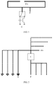
- FIG. 1 A tunable antenna based on an IFA (Inverted-F Antenna, inverted-F antenna) architecture in the prior art is shown in FIG. 1 .
- the IFA is a classic passive antenna.
- a single-pole and double-throw switch is serially connected to a ground point of the IFA, and an inductor or an invariable capacitor is serially connected by using the single-pole double-throw switch to implement grounding. That the IFA is grounded by using the inductor or the invariable capacitor necessarily changes an impedance property of the tunable antenna shown in FIG. 1 , thereby implementing a change of an operating band.
- a sum of bands that can be covered in all states of the antenna is antenna bandwidth.
- a low-frequency resonance frequency of the tunable antenna depends on a length of a long branch of an intermediate- or low-frequency radiator of radiators.
- a length of the radiator affects an overall size of the antenna. That is, in a case in which the size of the antenna is limited to some extent, the antenna bandwidth may be relatively narrow and cannot meet application requirements.
- Embodiments of the present invention provide an antenna and a terminal, so as to extend antenna bandwidth.
- an antenna including a capacitor component and at least one radiator, where
- the antenna further includes at least one matching circuit, one end of each matching circuit of the at least one matching circuit is connected to form a third node, the third node is connected to the other end of the capacitor component, and the other end of the capacitor component receives the feed signal by using each matching circuit of the at least one matching circuit, where
- the antenna further includes at least one tunable circuit, one end of each tunable circuit of the at least one tunable circuit is connected to form a fourth node, the fourth node is connected to the second node, and the second node is grounded by using each tunable circuit of the at least one tunable circuit, where
- the tunable circuit is specifically a matching circuit or a filter.
- the tunable circuit is specifically a single-pole double-throw switch, where a movable end of the single-pole double-throw switch serves as the one end of the tunable circuit that forms the fourth node, one immovable end of the single-pole double-throw switch serves as a grounding end of the tunable circuit, and the other immovable end of the single-pole double-throw switch is free.
- the tunable circuit specifically includes a first matching circuit, a second matching circuit, and a single-pole double-throw switch, where
- the tunable circuit specifically includes an input capacitor, a low-frequency capacitor, a high-frequency capacitor, and a single-pole double-throw switch, where
- the capacitor component specifically includes an interdigital capacitor and/or a variable capacitor.
- a terminal including any one of the foregoing described antennas.
- a capacitor component is added at a signal feed end of the antenna, and the capacitor component and a distributed inductor of a ground cable can generate low-frequency resonance.
- a frequency of the low-frequency resonance can be tuned by changing the capacitor component or the distributed inductor, without a need to change a length of a radiator. Therefore, in a case in which an antenna size is limited to some extent, the solution provided in the embodiments of the present invention can extend the antenna bandwidth.
- embodiments of the present invention provide an antenna and a terminal.
- the following describes exemplary embodiments of the present invention with reference to the accompanying drawings of this specification. It should be understood that the exemplary embodiments described herein are merely used to describe and explain the present invention, but are not intended to limit the present invention.
- the embodiments in this application and features in the embodiments may be combined with each other under circumstances of no conflicts.
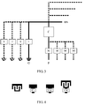
- An embodiment of the present invention provides an antenna, which, as shown in FIG. 2 , includes a capacitor component C and at least one radiator BN, where
- a node formed after the one end of each radiator BN is connected and then is connected to the one end of the capacitor component C serves as the second node, where the second node serves as a grounding end G of the antenna; and the other end of the capacitor component C serves as a signal feed end F of the antenna.
- the capacitor component C is added at the signal feed end F of the antenna.
- the capacitor component C and a distributed inductor of a ground cable can generate low-frequency resonance.
- a frequency of the low-frequency resonance can be tuned by changing the capacitor component C or the distributed inductor.
- the antenna further includes at least one matching circuit M, one end of each matching circuit M of the at least one matching circuit is connected to form a third node, the third node is connected to the other end of the capacitor component C, and the other end of the capacitor component C receives the feed signal by using each matching circuit M of the at least one matching circuit, where the matching circuit M includes an inductor and/or a capacitor.
- an inductor and a capacitor may exist in the matching circuit M, and a specific quantity of the inductors or capacitors and a manner of connecting them are not limited.
- Serial connection, parallel connection or hybrid connection of any quantity of inductors and capacitors may serve as a specific implementation manner of the matching circuit M in the antenna provided in this embodiment of the present invention.
- antenna bandwidth can be extended by serially connecting an inductor or capacitor at the signal feed end F.
- the antenna further includes at least one tunable circuit T, one end of each tunable circuit T of the at least one tunable circuit is connected to form a fourth node, the fourth node is connected to the second node, and the second node is grounded by using each tunable circuit T of the at least one tunable circuit, where the tunable circuit T is capacitive or inductive.
- the frequency of low-frequency resonance can be tuned, an impedance property of the antenna can be changed, and more tunable states of the antenna can be added.
- capacitor component C may be specifically implemented in multiple manners, and FIG. 4 enumerates four manners.
- the capacitor component C is specifically an interdigital capacitor whose bandwidth is relatively wide but invariable.
- the capacitor component C is specifically an invariable capacitor C 1 whose bandwidth is relatively narrow and invariable.
- the capacitor component C is specifically a variable capacitor VAC whose bandwidth is relatively narrow but variable.
- the capacitor component C specifically includes an interdigital capacitor and a variable capacitor VAC whose bandwidth is relatively wide and variable.
- the tunable circuit T may be specifically implemented in multiple manners, and FIG. 5 enumerates five manners.
- the tunable circuit T is specifically a matching circuit M, and preferably, the matching circuit M includes a variable capacitor.
- the tunable states are not limited. The more the tunable states, the wider the antenna bandwidth.
- the tunable circuit T is specifically a filter Filter. In this case, the tunable states are limited.
- the tunable circuit T is specifically a single-pole double-throw switch, where a movable end of the single-pole double-throw switch serves as the one end of the tunable circuit that forms the fourth node, one immovable end of the single-pole double-throw switch serves as a grounding end of the tunable circuit, and the other immovable end of the single-pole double-throw switch is free.
- a switching loss exists, and the tunable states are limited.
- the tunable circuit T specifically includes a first matching circuit M 1 , a second matching circuit M 2 , and a single-pole double-throw switch, where
- the tunable circuit T specifically includes an input capacitor C 0 , a low-frequency capacitor C L , a high-frequency capacitor C H , and a single-pole double-throw switch, where
- An antenna provided in Embodiment 1 of the present invention is applicable to GSM 900/1800/1900 and WCDMA 2100.
- FIG. 6 shows the antenna provided in Embodiment 1 of the present invention, which includes a capacitor component, two radiators BN 1 and BN 2 and a matching circuit M, where
- the variable capacitor VAC and a distributed inductor of a ground cable generate a low-frequency resonance frequency f 1 .
- the low-frequency resonance frequency f 1 can be tuned by changing the distributed inductor, that is, changing a length of the ground cable.
- the length of the ground cable is generally less than one eighth of a waveguide wavelength, and the waveguide wavelength is a signal wavelength of a center frequency of antenna applied bandwidth. In a given inductance value range, the greater the distributed inductance, the higher the low-frequency resonance frequency f 1 .
- the low-frequency resonance frequency f 1 is also fine-tunable by changing an capacitance value of the variable capacitor VAC. In a given capacitance value range, the greater the capacitance value of the variable capacitor VAC, the lower the low-frequency resonance frequency f 1 .
- a high-frequency resonance frequency f 2 can be generated; and by using the radiator BN 2 , a high-frequency resonance frequency f 3 can be generated.
- the high-frequency resonance frequencies f 2 and f 3 are slightly affected.
- bandwidth of the antenna provided in Embodiment 1 of the present invention is a band covered by the resonance frequencies f 1 , f 2 , and f 3 .
- An antenna provided in Embodiment 2 of the present invention is applicable to GSM/DCS/PCS/WCDMA/LTE.
- FIG. 7 shows the antenna provided in Embodiment 2 of the present invention, which includes a capacitor component, three radiators BN 1 , BN 2 , and BN 3 , a matching circuit M, and a tunable circuit, where the capacitor component is specifically an invariable capacitor C 1 , and the tunable circuit is specifically a variable capacitor VAC; five ends, that is, one end of the radiator BN 1 , one end of the radiator BN 2 , one end of the radiator BN 3 , one end of the variable capacitor VAC, and one end of the invariable capacitor C 1 , are connected; the other end of the invariable capacitor C 1 is connected to one end of the matching circuit M, and the other end of the matching circuit M serves as a signal feed end F of the antenna; and the other end of the variable capacitor VAC serves as a grounding end G of the antenna.
- the capacitor component is specifically an invariable capacitor C 1
- the tunable circuit is specifically a variable capacitor VAC
- the invariable capacitor C 1 and an inductor of a ground cable generate a low-frequency resonance frequency f 1 .
- An inductance value of the ground cable can be changed by changing a capacitance value of the variable capacitor VAC, and further, the low-frequency resonance frequency f 1 can be tuned. In a given capacitance value range, the greater the capacitance value of the variable capacitor VAC, the higher the low-frequency resonance frequency f 1 .
- a high-frequency resonance frequency can be generated; by using the radiator BN 2 , a high-frequency resonance frequency f 3 can be generated; and by using the radiator BN 3 , a high-frequency resonance frequency f 4 can be generated.
- the low-frequency resonance frequency f 1 is tuned by changing the tunable circuit, that is, by changing the capacitance value of the variable capacitor VAC, the high-frequency resonance frequencies f 2 , f 3 , and f 4 are not affected.
- bandwidth of the antenna provided in Embodiment 2 of the present invention is a band covered by the resonance frequencies f 1 , f 2 , f 3 , and f 4 .
- Embodiment 3 of the present invention further provides a terminal, including an antenna shown in any of FIG. 2 , FIG. 3 , FIG. 6 , and FIG. 7 .
Landscapes
- Engineering & Computer Science (AREA)
- Signal Processing (AREA)
- Computer Networks & Wireless Communication (AREA)
- Details Of Aerials (AREA)
- Input Circuits Of Receivers And Coupling Of Receivers And Audio Equipment (AREA)
- Waveguide Aerials (AREA)
- Transceivers (AREA)
Abstract
Description
- The present invention relates to the field of communications technologies, and in particular, to an antenna and a terminal.
- A terminal in a mobile communications network transmits and receives signals by using an antenna. With development and application of technologies, antenna bandwidth of a terminal product needs to cover more bands. In addition, in order to seek an esthetic appearance, space reserved for the antenna is increasingly smaller. Obviously, a traditional passive antenna can hardly meet requirements in an application scenario, and people pay more attention to a tunable antenna that combines a passive antenna and a tunable device.
- A tunable antenna based on an IFA (Inverted-F Antenna, inverted-F antenna) architecture in the prior art is shown in
FIG. 1 . The IFA is a classic passive antenna. A single-pole and double-throw switch is serially connected to a ground point of the IFA, and an inductor or an invariable capacitor is serially connected by using the single-pole double-throw switch to implement grounding. That the IFA is grounded by using the inductor or the invariable capacitor necessarily changes an impedance property of the tunable antenna shown inFIG. 1 , thereby implementing a change of an operating band. A sum of bands that can be covered in all states of the antenna is antenna bandwidth. - However, a low-frequency resonance frequency of the tunable antenna depends on a length of a long branch of an intermediate- or low-frequency radiator of radiators. A length of the radiator affects an overall size of the antenna. That is, in a case in which the size of the antenna is limited to some extent, the antenna bandwidth may be relatively narrow and cannot meet application requirements.
- Embodiments of the present invention provide an antenna and a terminal, so as to extend antenna bandwidth.
- According to a first aspect, an antenna is provided, including a capacitor component and at least one radiator, where
- one end of each radiator of the at least one radiator is connected to form a first node, the first node is connected to one end of the capacitor component to form a second node, and the second node is grounded; and
- the other end of the capacitor component receives a feed signal.
- With reference to the first aspect, in a first possible implementation manner, the antenna further includes at least one matching circuit, one end of each matching circuit of the at least one matching circuit is connected to form a third node, the third node is connected to the other end of the capacitor component, and the other end of the capacitor component receives the feed signal by using each matching circuit of the at least one matching circuit, where
- the matching circuit includes an inductor and/or a capacitor.
- With reference to the first aspect or the first possible implementation manner of the first aspect, in a second possible implementation manner, the antenna further includes at least one tunable circuit, one end of each tunable circuit of the at least one tunable circuit is connected to form a fourth node, the fourth node is connected to the second node, and the second node is grounded by using each tunable circuit of the at least one tunable circuit, where
- the tunable circuit is capacitive or inductive.
- With reference to the second possible implementation manner of the first aspect, in a third possible implementation manner, the tunable circuit is specifically a matching circuit or a filter.
- With reference to the second possible implementation manner of the first aspect, in a fourth possible implementation manner, the tunable circuit is specifically a single-pole double-throw switch, where a movable end of the single-pole double-throw switch serves as the one end of the tunable circuit that forms the fourth node, one immovable end of the single-pole double-throw switch serves as a grounding end of the tunable circuit, and the other immovable end of the single-pole double-throw switch is free.
- With reference to the second possible implementation manner of the first aspect, in a fifth possible implementation manner, the tunable circuit specifically includes a first matching circuit, a second matching circuit, and a single-pole double-throw switch, where
- a movable end of the single-pole double-throw switch serves as the one end of the tunable circuit that forms the fourth node;
- two immovable ends of the single-pole double-throw switch are connected to one end of the first matching circuit and one end of the second matching circuit respectively; and
- the other end of the first matching circuit is connected to another end of the second matching circuit to form a fifth node, and the fifth node serves as a grounding end of the tunable circuit.
- With reference to the second possible implementation manner of the first aspect, in a sixth possible implementation manner, the tunable circuit specifically includes an input capacitor, a low-frequency capacitor, a high-frequency capacitor, and a single-pole double-throw switch, where
- one end of the input capacitor is connected to a movable end of the single-pole double-throw switch, and the other end of the input capacitor serves as the one end of the tunable circuit that forms the fourth node; and
- one end of the low-frequency capacitor and one end of the high-frequency capacitor are connected to two immovable ends of the single-pole double-throw switch respectively, the other end of the low-frequency capacitor is connected to the other end of the high-frequency capacitor to form a sixth node, and the sixth node serves as a grounding end of the tunable circuit.
- With reference to the first aspect, or the second possible implementation manner of the first aspect, or the third possible implementation manner of the first aspect, or the fourth possible implementation manner of the first aspect, or the fifth possible implementation manner of the first aspect, or the sixth possible implementation manner of the first aspect, in a seventh possible implementation manner, the capacitor component specifically includes an interdigital capacitor and/or a variable capacitor.
- According to a second aspect, a terminal is provided, including any one of the foregoing described antennas.
- According to the antenna provided in the first aspect or the terminal provided in the second aspect, a capacitor component is added at a signal feed end of the antenna, and the capacitor component and a distributed inductor of a ground cable can generate low-frequency resonance. A frequency of the low-frequency resonance can be tuned by changing the capacitor component or the distributed inductor, without a need to change a length of a radiator. Therefore, in a case in which an antenna size is limited to some extent, the solution provided in the embodiments of the present invention can extend the antenna bandwidth.
- The accompanying drawings are intended for further understanding of the present invention, and constitute a part of this specification. They are used together with the embodiments of the present invention to interpret the present invention but do not constitute any limitation on the present invention. In the accompanying drawings:
-
FIG. 1 is a schematic diagram of an antenna in the prior art; -
FIG. 2 is a first schematic diagram of an antenna according to an embodiment of the present invention; -
FIG. 3 is a second schematic diagram of an antenna according to an embodiment of the present invention; -
FIG. 4 is a schematic diagram of a capacitor component in an antenna according to an embodiment of the present invention; -
FIG. 5 is a schematic diagram of a tunable circuit in an antenna according to an embodiment of the present invention; -
FIG. 6 is a schematic diagram of an antenna according to Embodiment 1 of the present invention; and -
FIG. 7 is a schematic diagram of an antenna according to Embodiment 2 of the present invention. - To give a solution to extending antenna bandwidth, embodiments of the present invention provide an antenna and a terminal. The following describes exemplary embodiments of the present invention with reference to the accompanying drawings of this specification. It should be understood that the exemplary embodiments described herein are merely used to describe and explain the present invention, but are not intended to limit the present invention. The embodiments in this application and features in the embodiments may be combined with each other under circumstances of no conflicts.
- An embodiment of the present invention provides an antenna, which, as shown in
FIG. 2 , includes a capacitor component C and at least one radiator BN, where - one end of each radiator BN of the at least one radiator is connected to form a first node, the first node is connected to one end of the capacitor component C to form a second node, and the second node is grounded; and
- the other end of the capacitor component C receives a feed signal.
- That is, a node formed after the one end of each radiator BN is connected and then is connected to the one end of the capacitor component C serves as the second node, where the second node serves as a grounding end G of the antenna; and the other end of the capacitor component C serves as a signal feed end F of the antenna.
- The capacitor component C is added at the signal feed end F of the antenna. The capacitor component C and a distributed inductor of a ground cable can generate low-frequency resonance. A frequency of the low-frequency resonance can be tuned by changing the capacitor component C or the distributed inductor.
- Preferably, as shown in
FIG. 3 , the antenna further includes at least one matching circuit M, one end of each matching circuit M of the at least one matching circuit is connected to form a third node, the third node is connected to the other end of the capacitor component C, and the other end of the capacitor component C receives the feed signal by using each matching circuit M of the at least one matching circuit, where the matching circuit M includes an inductor and/or a capacitor. - That is, two types of devices: an inductor and a capacitor, may exist in the matching circuit M, and a specific quantity of the inductors or capacitors and a manner of connecting them are not limited. Serial connection, parallel connection or hybrid connection of any quantity of inductors and capacitors may serve as a specific implementation manner of the matching circuit M in the antenna provided in this embodiment of the present invention.
- With the matching circuit M added, antenna bandwidth can be extended by serially connecting an inductor or capacitor at the signal feed end F.
- Preferably, as shown in
FIG. 3 , the antenna further includes at least one tunable circuit T, one end of each tunable circuit T of the at least one tunable circuit is connected to form a fourth node, the fourth node is connected to the second node, and the second node is grounded by using each tunable circuit T of the at least one tunable circuit, where the tunable circuit T is capacitive or inductive. - By using the tunable circuit T, the frequency of low-frequency resonance can be tuned, an impedance property of the antenna can be changed, and more tunable states of the antenna can be added.
- Further, the capacitor component C may be specifically implemented in multiple manners, and
FIG. 4 enumerates four manners. - In a first implementation manner of the capacitor component C, the capacitor component C is specifically an interdigital capacitor whose bandwidth is relatively wide but invariable.
- In a second implementation manner of the capacitor component C, the capacitor component C is specifically an invariable capacitor C1 whose bandwidth is relatively narrow and invariable.
- In a third implementation manner of the capacitor component C, the capacitor component C is specifically a variable capacitor VAC whose bandwidth is relatively narrow but variable.
- Preferably, in a fourth implementation manner of the capacitor component C, the capacitor component C specifically includes an interdigital capacitor and a variable capacitor VAC whose bandwidth is relatively wide and variable.
- The foregoing four specific implementation manners are merely exemplary, and are not intended to limit the present invention. Any other capacitor-type device or a combination of capacitor-type devices may serve as a specific implementation manner of the capacitor component C in the antenna provided in this embodiment of the present invention.
- Further, the tunable circuit T may be specifically implemented in multiple manners, and
FIG. 5 enumerates five manners. - In a first implementation manner of the tunable circuit T, the tunable circuit T is specifically a matching circuit M, and preferably, the matching circuit M includes a variable capacitor. When the matching circuit M includes a variable capacitor, the tunable states are not limited. The more the tunable states, the wider the antenna bandwidth.
- In a second implementation manner of the tunable circuit T, the tunable circuit T is specifically a filter Filter. In this case, the tunable states are limited.
- In a third implementation manner of the tunable circuit T, the tunable circuit T is specifically a single-pole double-throw switch, where a movable end of the single-pole double-throw switch serves as the one end of the tunable circuit that forms the fourth node, one immovable end of the single-pole double-throw switch serves as a grounding end of the tunable circuit, and the other immovable end of the single-pole double-throw switch is free. In this case, a switching loss exists, and the tunable states are limited.
- In a fourth implementation manner of the tunable circuit T, the tunable circuit T specifically includes a first matching circuit M1, a second matching circuit M2, and a single-pole double-throw switch, where
- a movable end of the single-pole double-throw switch serves as the one end of the tunable circuit that forms the fourth node; two immovable ends of the single-pole double-throw switch are connected to one end of the first matching circuit and one end of the second matching circuit respectively; and the other end of the first matching circuit is connected to another end of the second matching circuit to form a fifth node, and the fifth node serves as a grounding end of the tunable circuit. In this case, a switching loss exists, and the tunable states depend on specific implementation of the two matching circuits.
- In a fifth implementation manner of the tunable circuit T, the tunable circuit T specifically includes an input capacitor C0, a low-frequency capacitor CL, a high-frequency capacitor CH, and a single-pole double-throw switch, where
- one end of the input capacitor is connected to a movable end of the single-pole double-throw switch, and the other end of the input capacitor serves as the one end of the tunable circuit that forms the fourth node; and one end of the low-frequency capacitor and one end of the high-frequency capacitor are connected to two immovable ends of the single-pole double-throw switch respectively, the other end of the low-frequency capacitor is connected to the other end of the high-frequency capacitor to form a sixth node, and the sixth node serves as a grounding end of the tunable circuit. In this case, a switching loss exists, and the tunable states are limited.
- The foregoing five specific implementation manners are merely exemplary, and are not intended to limit the present invention. Any other capacitive or inductive device or circuit may serve as a specific implementation manner of the tunable circuit T in the antenna provided in this embodiment of the present invention.
- The following elaborates on the antenna provided in the present invention with reference to the accompanying drawings by using specific embodiments.
- An antenna provided in Embodiment 1 of the present invention is applicable to GSM 900/1800/1900 and WCDMA 2100.
-
FIG. 6 shows the antenna provided in Embodiment 1 of the present invention, which includes a capacitor component, two radiators BN1 and BN2 and a matching circuit M, where - the capacitor component is specifically a variable capacitor VAC;
- one end of the radiator BN1, one end of the radiator BN2, and one end of the variable capacitor VAC are connected, and a node formed after the three ends are connected serves as a grounding end G of the antenna; and
- the other end of the variable capacitor VAC is connected to one end of the matching circuit M, and another end of the matching circuit M serves as a signal feed end F of the antenna.
- In the antenna provided in Embodiment 1 of the present invention, the variable capacitor VAC and a distributed inductor of a ground cable generate a low-frequency resonance frequency f1.
- The low-frequency resonance frequency f1 can be tuned by changing the distributed inductor, that is, changing a length of the ground cable. Experiments prove that the length of the ground cable is generally less than one eighth of a waveguide wavelength, and the waveguide wavelength is a signal wavelength of a center frequency of antenna applied bandwidth. In a given inductance value range, the greater the distributed inductance, the higher the low-frequency resonance frequency f1.
- The low-frequency resonance frequency f1 is also fine-tunable by changing an capacitance value of the variable capacitor VAC. In a given capacitance value range, the greater the capacitance value of the variable capacitor VAC, the lower the low-frequency resonance frequency f1.
- By using the radiator BN1, a high-frequency resonance frequency f2 can be generated; and by using the radiator BN2, a high-frequency resonance frequency f3 can be generated.
- When the low-frequency resonance frequency f1 is tuned by changing the capacitance value of the capacitor component, that is, the variable capacitor VAC, the high-frequency resonance frequencies f2 and f3 are slightly affected.
- That is, bandwidth of the antenna provided in Embodiment 1 of the present invention is a band covered by the resonance frequencies f1, f2, and f3.
- An antenna provided in Embodiment 2 of the present invention is applicable to GSM/DCS/PCS/WCDMA/LTE.
-
FIG. 7 shows the antenna provided in Embodiment 2 of the present invention, which includes a capacitor component, three radiators BN1, BN2, and BN3, a matching circuit M, and a tunable circuit, where
the capacitor component is specifically an invariable capacitor C1, and the tunable circuit is specifically a variable capacitor VAC;
five ends, that is, one end of the radiator BN1, one end of the radiator BN2, one end of the radiator BN3, one end of the variable capacitor VAC, and one end of the invariable capacitor C1, are connected;
the other end of the invariable capacitor C1 is connected to one end of the matching circuit M, and the other end of the matching circuit M serves as a signal feed end F of the antenna; and
the other end of the variable capacitor VAC serves as a grounding end G of the antenna. - In the antenna provided in Embodiment 2 of the present invention, the invariable capacitor C1 and an inductor of a ground cable generate a low-frequency resonance frequency f1.
- An inductance value of the ground cable can be changed by changing a capacitance value of the variable capacitor VAC, and further, the low-frequency resonance frequency f1 can be tuned. In a given capacitance value range, the greater the capacitance value of the variable capacitor VAC, the higher the low-frequency resonance frequency f1.
- By using the radiator BN1, a high-frequency resonance frequency can be generated; by using the radiator BN2, a high-frequency resonance frequency f3 can be generated; and by using the radiator BN3, a high-frequency resonance frequency f4 can be generated.
- When the low-frequency resonance frequency f1 is tuned by changing the tunable circuit, that is, by changing the capacitance value of the variable capacitor VAC, the high-frequency resonance frequencies f2, f3, and f4 are not affected.
- That is, bandwidth of the antenna provided in Embodiment 2 of the present invention is a band covered by the resonance frequencies f1, f2, f3, and f4.
- It can be seen that, in a case in which an antenna size is limited to some extent, the solution provided in this embodiment of the present invention can extend the bandwidth and meet requirements of more application scenarios.
- Embodiment 3 of the present invention further provides a terminal, including an antenna shown in any of
FIG. 2 ,FIG. 3 ,FIG. 6 , andFIG. 7 . - Persons skilled in the art should understand that, although some exemplary embodiments of the present invention have been described, the persons skilled in the art can make changes and modifications to these embodiments once they learn the basic inventive concept. Therefore, the following claims are intended to be construed as to cover the exemplary embodiments and all changes and modifications falling within the scope of the present invention.
- Obviously, persons skilled in the art can make various modifications and variations to the embodiments of the present invention without departing from the spirit and scope of the embodiments of the present invention. The present invention is intended to cover these modifications and variations provided that they fall within the scope of protection defined by the following claims and their equivalent technologies.
Claims (9)
- An antenna, comprising a capacitor component and at least one radiator, wherein
one end of each radiator of the at least one radiator is connected to form a first node, the first node is connected to one end of the capacitor component to form a second node, and the second node is grounded; and
the other end of the capacitor component receives a feed signal. - The antenna according to claim 1, wherein the antenna further comprises at least one matching circuit, one end of each matching circuit of the at least one matching circuit is connected to form a third node, the third node is connected to the other end of the capacitor component, and the other end of the capacitor component receives the feed signal by using each matching circuit of the at least one matching circuit, wherein
the matching circuit comprises an inductor and/or a capacitor. - The antenna according to claim 1 or 2, wherein the antenna further comprises at least one tunable circuit, one end of each tunable circuit of the at least one tunable circuit is connected to form a fourth node, the fourth node is connected to the second node, and the second node is grounded by using each tunable circuit of the at least one tunable circuit, wherein
the tunable circuit is capacitive or inductive. - The antenna according to claim 3, wherein the tunable circuit is specifically a matching circuit or a filter.
- The antenna according to claim 3, wherein the tunable circuit is specifically a single-pole double-throw switch, wherein a movable end of the single-pole double-throw switch serves as the one end of the tunable circuit that forms the fourth node, one immovable end of the single-pole double-throw switch serves as a grounding end of the tunable circuit, and the other immovable end of the single-pole double-throw switch is free.
- The antenna according to claim 3, wherein the tunable circuit specifically comprises a first matching circuit, a second matching circuit, and a single-pole double-throw switch, wherein
a movable end of the single-pole double-throw switch serves as the one end of the tunable circuit that forms the fourth node;
two immovable ends of the single-pole double-throw switch are connected to one end of the first matching circuit and one end of the second matching circuit respectively; and
the other end of the first matching circuit is connected to another end of the second matching circuit to form a fifth node, and the fifth node serves as a grounding end of the tunable circuit. - The antenna according to claim 3, wherein the tunable circuit specifically comprises an input capacitor, a low-frequency capacitor, a high-frequency capacitor, and a single-pole double-throw switch, wherein
one end of the input capacitor is connected to a movable end of the single-pole double-throw switch, and the other end of the input capacitor serves as the one end of the tunable circuit that forms the fourth node; and
one end of the low-frequency capacitor and one end of the high-frequency capacitor are connected to two immovable ends of the single-pole double-throw switch respectively, the other end of the low-frequency capacitor is connected to the other end of the high-frequency capacitor to form a sixth node, and the sixth node serves as a grounding end of the tunable circuit. - The antenna according to any one of claims 1 to 7, wherein the capacitor component specifically comprises an interdigital capacitor and/or a variable capacitor.
- A terminal, comprising the antenna according to any one of claims 1 to 8.
Priority Applications (1)
| Application Number | Priority Date | Filing Date | Title |
|---|---|---|---|
| EP18191759.2A EP3487002A1 (en) | 2013-12-20 | 2013-12-20 | Antenna and terminal |
Applications Claiming Priority (1)
| Application Number | Priority Date | Filing Date | Title |
|---|---|---|---|
| PCT/CN2013/090144 WO2015089841A1 (en) | 2013-12-20 | 2013-12-20 | Antenna and terminal |
Related Child Applications (2)
| Application Number | Title | Priority Date | Filing Date |
|---|---|---|---|
| EP18191759.2A Division-Into EP3487002A1 (en) | 2013-12-20 | 2013-12-20 | Antenna and terminal |
| EP18191759.2A Division EP3487002A1 (en) | 2013-12-20 | 2013-12-20 | Antenna and terminal |
Publications (3)
| Publication Number | Publication Date |
|---|---|
| EP3070785A1 true EP3070785A1 (en) | 2016-09-21 |
| EP3070785A4 EP3070785A4 (en) | 2016-12-28 |
| EP3070785B1 EP3070785B1 (en) | 2018-11-07 |
Family
ID=51710607
Family Applications (2)
| Application Number | Title | Priority Date | Filing Date |
|---|---|---|---|
| EP18191759.2A Withdrawn EP3487002A1 (en) | 2013-12-20 | 2013-12-20 | Antenna and terminal |
| EP13899968.5A Active EP3070785B1 (en) | 2013-12-20 | 2013-12-20 | Antenna and terminal |
Family Applications Before (1)
| Application Number | Title | Priority Date | Filing Date |
|---|---|---|---|
| EP18191759.2A Withdrawn EP3487002A1 (en) | 2013-12-20 | 2013-12-20 | Antenna and terminal |
Country Status (6)
| Country | Link |
|---|---|
| US (2) | US10283864B2 (en) |
| EP (2) | EP3487002A1 (en) |
| JP (1) | JP6332881B2 (en) |
| KR (1) | KR101821077B1 (en) |
| CN (1) | CN104115331B (en) |
| WO (1) | WO2015089841A1 (en) |
Cited By (1)
| Publication number | Priority date | Publication date | Assignee | Title |
|---|---|---|---|---|
| EP3422471A1 (en) * | 2017-06-27 | 2019-01-02 | Beijing Xiaomi Mobile Software Co., Ltd. | Antenna and electronic device |
Families Citing this family (10)
| Publication number | Priority date | Publication date | Assignee | Title |
|---|---|---|---|---|
| CN105811079B (en) * | 2014-12-31 | 2020-05-26 | 联想(北京)有限公司 | Antenna device and electronic equipment |
| EP3229314B1 (en) * | 2015-01-04 | 2019-08-14 | Huawei Technologies Co. Ltd. | Handheld device |
| CN106159450A (en) * | 2015-03-26 | 2016-11-23 | 联想(北京)有限公司 | Loop aerial and electronic equipment |
| US10109914B2 (en) * | 2015-03-27 | 2018-10-23 | Intel IP Corporation | Antenna system |
| CN105470635B (en) * | 2015-12-11 | 2022-11-18 | 北京伯临通信科技有限公司 | Low-profile dual-frequency high-precision multimode navigation antenna |
| US11177568B2 (en) | 2017-04-01 | 2021-11-16 | Huawei Technologies Co., Ltd. | Antenna resource scheduling method and device |
| JP2019047265A (en) * | 2017-08-31 | 2019-03-22 | 株式会社ヨコオ | Antenna device and inverted F antenna |
| CN109273841B (en) * | 2018-09-17 | 2020-12-04 | 深圳传音通讯有限公司 | Antenna and terminal equipment |
| CN114665251B (en) * | 2020-03-31 | 2025-08-05 | 华为技术有限公司 | Antenna and terminal |
| CN116345122B (en) | 2021-12-22 | 2025-05-20 | 荣耀终端股份有限公司 | Foldable electronic device and antenna system thereof |
Family Cites Families (30)
| Publication number | Priority date | Publication date | Assignee | Title |
|---|---|---|---|---|
| JPH1028013A (en) * | 1996-07-11 | 1998-01-27 | Matsushita Electric Ind Co Ltd | Planar antenna |
| JPH10107671A (en) * | 1996-09-26 | 1998-04-24 | Kokusai Electric Co Ltd | Antenna for portable wireless terminal |
| JP3430140B2 (en) * | 2000-10-05 | 2003-07-28 | 埼玉日本電気株式会社 | Inverted-F antenna and wireless device using the same |
| US7174147B2 (en) * | 2001-04-11 | 2007-02-06 | Kyocera Wireless Corp. | Bandpass filter with tunable resonator |
| JP2003249811A (en) * | 2001-12-20 | 2003-09-05 | Murata Mfg Co Ltd | Double-resonance antenna apparatus |
| JP2004266311A (en) * | 2003-01-15 | 2004-09-24 | Fdk Corp | Antenna |
| TW200537735A (en) | 2003-12-25 | 2005-11-16 | Mitsubishi Materials Corp | Antenna device and communication apparatus |
| JP4089680B2 (en) * | 2003-12-25 | 2008-05-28 | 三菱マテリアル株式会社 | Antenna device |
| CN101212230B (en) * | 2006-12-26 | 2012-07-11 | 中兴通讯股份有限公司 | Device and method for implementing DVB-H antenna matching network for mobile telephone |
| JP2008258670A (en) * | 2007-03-30 | 2008-10-23 | Matsushita Electric Ind Co Ltd | Antenna device and portable terminal |
| CN201060933Y (en) * | 2007-04-09 | 2008-05-14 | 樊明延 | Balanced type dual-branch plane inverse F type antenna |
| FI120427B (en) * | 2007-08-30 | 2009-10-15 | Pulse Finland Oy | Adjustable multiband antenna |
| JP2009278192A (en) * | 2008-05-12 | 2009-11-26 | Sony Ericsson Mobilecommunications Japan Inc | Antenna device and communication terminal |
| CN201374385Y (en) * | 2008-11-21 | 2009-12-30 | 富港电子(东莞)有限公司 | Antenna with a shield |
| EP2234205A1 (en) | 2009-03-24 | 2010-09-29 | Laird Technologies AB | An antenna device and a portable radio communication device comprising such antenna device |
| US8405568B2 (en) * | 2009-05-29 | 2013-03-26 | Intel Mobile Communications GmbH | Wireless communication device antenna with tuning elements |
| JP5321290B2 (en) | 2009-06-30 | 2013-10-23 | 株式会社村田製作所 | Antenna structure |
| US9252494B2 (en) | 2009-11-13 | 2016-02-02 | Hitachi Metals, Ltd. | Frequency-variable antenna circuit, antenna device constituting it, and wireless communications apparatus comprising it |
| CN102918709B (en) | 2010-04-06 | 2015-08-19 | 拉迪娜股份有限公司 | Antenna feed structure and antenna |
| TWM408886U (en) * | 2011-01-06 | 2011-08-01 | Wistron Corp | Antenna switching device and mobile communication device having antenna switching device |
| JP5626024B2 (en) * | 2011-03-02 | 2014-11-19 | 船井電機株式会社 | Multi-antenna device and communication device |
| US9246221B2 (en) * | 2011-03-07 | 2016-01-26 | Apple Inc. | Tunable loop antennas |
| JP5301608B2 (en) * | 2011-05-24 | 2013-09-25 | レノボ・シンガポール・プライベート・リミテッド | Antenna for wireless terminal equipment |
| TWI487198B (en) * | 2011-06-03 | 2015-06-01 | Wistron Neweb Corp | A multi-band antenna |
| JP2013017112A (en) * | 2011-07-06 | 2013-01-24 | Hitachi Metals Ltd | Antenna and radio communication device using the same |
| US8570227B1 (en) * | 2011-09-15 | 2013-10-29 | The United States Of America As Represented By The Secretary Of The Navy | High-frequency transmit antenna system |
| KR101318575B1 (en) * | 2011-11-16 | 2013-10-16 | 주식회사 팬택 | Mobile terminal having antenna for tunning resonance frequency band and operating method there of |
| TWI491107B (en) | 2011-12-20 | 2015-07-01 | Wistron Neweb Corp | Tunable antenna and radio-frequency device |
| JP5637565B2 (en) | 2011-11-22 | 2014-12-10 | Necプラットフォームズ株式会社 | Multiband antenna and mobile terminal |
| US9270012B2 (en) * | 2012-02-01 | 2016-02-23 | Apple Inc. | Electronic device with calibrated tunable antenna |
-
2013
- 2013-12-20 KR KR1020167018958A patent/KR101821077B1/en active Active
- 2013-12-20 EP EP18191759.2A patent/EP3487002A1/en not_active Withdrawn
- 2013-12-20 WO PCT/CN2013/090144 patent/WO2015089841A1/en not_active Ceased
- 2013-12-20 JP JP2016541285A patent/JP6332881B2/en active Active
- 2013-12-20 CN CN201380008276.8A patent/CN104115331B/en active Active
- 2013-12-20 EP EP13899968.5A patent/EP3070785B1/en active Active
-
2016
- 2016-06-17 US US15/186,123 patent/US10283864B2/en active Active
-
2018
- 2018-10-19 US US16/165,256 patent/US20190051986A1/en not_active Abandoned
Cited By (2)
| Publication number | Priority date | Publication date | Assignee | Title |
|---|---|---|---|---|
| EP3422471A1 (en) * | 2017-06-27 | 2019-01-02 | Beijing Xiaomi Mobile Software Co., Ltd. | Antenna and electronic device |
| US10680330B2 (en) | 2017-06-27 | 2020-06-09 | Beijing Xiaomi Mobile Software Co., Ltd. | Antenna and electronic device |
Also Published As
| Publication number | Publication date |
|---|---|
| CN104115331B (en) | 2016-09-28 |
| US20160301134A1 (en) | 2016-10-13 |
| JP6332881B2 (en) | 2018-05-30 |
| US10283864B2 (en) | 2019-05-07 |
| KR101821077B1 (en) | 2018-01-22 |
| WO2015089841A1 (en) | 2015-06-25 |
| CN104115331A (en) | 2014-10-22 |
| KR20160099648A (en) | 2016-08-22 |
| JP2017505034A (en) | 2017-02-09 |
| EP3070785B1 (en) | 2018-11-07 |
| EP3487002A1 (en) | 2019-05-22 |
| US20190051986A1 (en) | 2019-02-14 |
| EP3070785A4 (en) | 2016-12-28 |
Similar Documents
| Publication | Publication Date | Title |
|---|---|---|
| US10283864B2 (en) | Antenna and terminal | |
| US11854728B2 (en) | Tunable inductor arrangement, transceiver, method and computer program | |
| US11949172B2 (en) | Antenna system and terminal | |
| US20180241368A1 (en) | Multi-harmonic matching networks | |
| CN112968678B (en) | A radio frequency power amplifier and a communication terminal | |
| CN108155478A (en) | Antenna and mobile terminal applied to mobile terminal | |
| CN105390810B (en) | A kind of antenna and terminal for receiving and dispatching multiband wireless signal | |
| US9455686B1 (en) | Wireless communication device and tunable filter thereof | |
| KR102600021B1 (en) | Band pass filter of variable band split | |
| KR101295229B1 (en) | Variable impedance matching circuit | |
| US9768753B2 (en) | Filter using BAWRs and L/C elements connected to the BAWRs | |
| JP6568259B2 (en) | Antenna and terminal device | |
| JP7183349B2 (en) | Filters and electronics | |
| CN103296488B (en) | Feed network device, antenna feed system and base station | |
| RU2496226C1 (en) | Multiband tunable lc bandpass filter | |
| Deng et al. | Generalized synthesis method for tunable and reconfigurable filter with flexible frequency response characteristics | |
| JP2005269387A (en) | Diplexer | |
| CN107534426A (en) | With the filter arrangement to bad electrically grounded compensation |
Legal Events
| Date | Code | Title | Description |
|---|---|---|---|
| PUAI | Public reference made under article 153(3) epc to a published international application that has entered the european phase |
Free format text: ORIGINAL CODE: 0009012 |
|
| 17P | Request for examination filed |
Effective date: 20160617 |
|
| AK | Designated contracting states |
Kind code of ref document: A1 Designated state(s): AL AT BE BG CH CY CZ DE DK EE ES FI FR GB GR HR HU IE IS IT LI LT LU LV MC MK MT NL NO PL PT RO RS SE SI SK SM TR |
|
| AX | Request for extension of the european patent |
Extension state: BA ME |
|
| A4 | Supplementary search report drawn up and despatched |
Effective date: 20161129 |
|
| RIC1 | Information provided on ipc code assigned before grant |
Ipc: H01Q 5/328 20150101ALI20161123BHEP Ipc: H01Q 1/38 20060101AFI20161123BHEP Ipc: H01Q 1/24 20060101ALI20161123BHEP Ipc: H01Q 5/335 20150101ALI20161123BHEP |
|
| DAX | Request for extension of the european patent (deleted) | ||
| RIC1 | Information provided on ipc code assigned before grant |
Ipc: H01Q 5/335 20150101ALI20170928BHEP Ipc: H01Q 1/38 20060101AFI20170928BHEP Ipc: H01Q 5/328 20150101ALI20170928BHEP Ipc: H01Q 1/24 20060101ALI20170928BHEP |
|
| RAP1 | Party data changed (applicant data changed or rights of an application transferred) |
Owner name: HUAWEI DEVICE (DONGGUAN) CO., LTD. |
|
| 17Q | First examination report despatched |
Effective date: 20171030 |
|
| RIN1 | Information on inventor provided before grant (corrected) |
Inventor name: WANG, HANYANG Inventor name: FENG, KUN Inventor name: ZHANG, XIAOJU Inventor name: LEE, CHIEN-MING |
|
| GRAP | Despatch of communication of intention to grant a patent |
Free format text: ORIGINAL CODE: EPIDOSNIGR1 |
|
| INTG | Intention to grant announced |
Effective date: 20180528 |
|
| GRAS | Grant fee paid |
Free format text: ORIGINAL CODE: EPIDOSNIGR3 |
|
| GRAA | (expected) grant |
Free format text: ORIGINAL CODE: 0009210 |
|
| AK | Designated contracting states |
Kind code of ref document: B1 Designated state(s): AL AT BE BG CH CY CZ DE DK EE ES FI FR GB GR HR HU IE IS IT LI LT LU LV MC MK MT NL NO PL PT RO RS SE SI SK SM TR |
|
| REG | Reference to a national code |
Ref country code: GB Ref legal event code: FG4D |
|
| REG | Reference to a national code |
Ref country code: CH Ref legal event code: EP Ref country code: AT Ref legal event code: REF Ref document number: 1063195 Country of ref document: AT Kind code of ref document: T Effective date: 20181115 |
|
| REG | Reference to a national code |
Ref country code: DE Ref legal event code: R096 Ref document number: 602013046530 Country of ref document: DE |
|
| REG | Reference to a national code |
Ref country code: IE Ref legal event code: FG4D |
|
| REG | Reference to a national code |
Ref country code: NL Ref legal event code: FP |
|
| REG | Reference to a national code |
Ref country code: LT Ref legal event code: MG4D |
|
| REG | Reference to a national code |
Ref country code: AT Ref legal event code: MK05 Ref document number: 1063195 Country of ref document: AT Kind code of ref document: T Effective date: 20181107 |
|
| PG25 | Lapsed in a contracting state [announced via postgrant information from national office to epo] |
Ref country code: IS Free format text: LAPSE BECAUSE OF FAILURE TO SUBMIT A TRANSLATION OF THE DESCRIPTION OR TO PAY THE FEE WITHIN THE PRESCRIBED TIME-LIMIT Effective date: 20190307 Ref country code: FI Free format text: LAPSE BECAUSE OF FAILURE TO SUBMIT A TRANSLATION OF THE DESCRIPTION OR TO PAY THE FEE WITHIN THE PRESCRIBED TIME-LIMIT Effective date: 20181107 Ref country code: NO Free format text: LAPSE BECAUSE OF FAILURE TO SUBMIT A TRANSLATION OF THE DESCRIPTION OR TO PAY THE FEE WITHIN THE PRESCRIBED TIME-LIMIT Effective date: 20190207 Ref country code: HR Free format text: LAPSE BECAUSE OF FAILURE TO SUBMIT A TRANSLATION OF THE DESCRIPTION OR TO PAY THE FEE WITHIN THE PRESCRIBED TIME-LIMIT Effective date: 20181107 Ref country code: LT Free format text: LAPSE BECAUSE OF FAILURE TO SUBMIT A TRANSLATION OF THE DESCRIPTION OR TO PAY THE FEE WITHIN THE PRESCRIBED TIME-LIMIT Effective date: 20181107 Ref country code: BG Free format text: LAPSE BECAUSE OF FAILURE TO SUBMIT A TRANSLATION OF THE DESCRIPTION OR TO PAY THE FEE WITHIN THE PRESCRIBED TIME-LIMIT Effective date: 20190207 Ref country code: ES Free format text: LAPSE BECAUSE OF FAILURE TO SUBMIT A TRANSLATION OF THE DESCRIPTION OR TO PAY THE FEE WITHIN THE PRESCRIBED TIME-LIMIT Effective date: 20181107 Ref country code: AT Free format text: LAPSE BECAUSE OF FAILURE TO SUBMIT A TRANSLATION OF THE DESCRIPTION OR TO PAY THE FEE WITHIN THE PRESCRIBED TIME-LIMIT Effective date: 20181107 Ref country code: LV Free format text: LAPSE BECAUSE OF FAILURE TO SUBMIT A TRANSLATION OF THE DESCRIPTION OR TO PAY THE FEE WITHIN THE PRESCRIBED TIME-LIMIT Effective date: 20181107 |
|
| PG25 | Lapsed in a contracting state [announced via postgrant information from national office to epo] |
Ref country code: PT Free format text: LAPSE BECAUSE OF FAILURE TO SUBMIT A TRANSLATION OF THE DESCRIPTION OR TO PAY THE FEE WITHIN THE PRESCRIBED TIME-LIMIT Effective date: 20190307 Ref country code: AL Free format text: LAPSE BECAUSE OF FAILURE TO SUBMIT A TRANSLATION OF THE DESCRIPTION OR TO PAY THE FEE WITHIN THE PRESCRIBED TIME-LIMIT Effective date: 20181107 Ref country code: RS Free format text: LAPSE BECAUSE OF FAILURE TO SUBMIT A TRANSLATION OF THE DESCRIPTION OR TO PAY THE FEE WITHIN THE PRESCRIBED TIME-LIMIT Effective date: 20181107 Ref country code: SE Free format text: LAPSE BECAUSE OF FAILURE TO SUBMIT A TRANSLATION OF THE DESCRIPTION OR TO PAY THE FEE WITHIN THE PRESCRIBED TIME-LIMIT Effective date: 20181107 Ref country code: GR Free format text: LAPSE BECAUSE OF FAILURE TO SUBMIT A TRANSLATION OF THE DESCRIPTION OR TO PAY THE FEE WITHIN THE PRESCRIBED TIME-LIMIT Effective date: 20190208 |
|
| RAP2 | Party data changed (patent owner data changed or rights of a patent transferred) |
Owner name: HUAWEI DEVICE CO., LTD. |
|
| REG | Reference to a national code |
Ref country code: NL Ref legal event code: HC Owner name: HUAWEI DEVICE CO., LTD.; CN Free format text: DETAILS ASSIGNMENT: CHANGE OF OWNER(S), CHANGE OF OWNER(S) NAME; FORMER OWNER NAME: HUAWEI DEVICE (DONGGUAN) CO., LTD. Effective date: 20190514 |
|
| REG | Reference to a national code |
Ref country code: DE Ref legal event code: R081 Ref document number: 602013046530 Country of ref document: DE Owner name: HUAWEI DEVICE CO., LTD., DONGGUAN, CN Free format text: FORMER OWNER: HUAWEI DEVICE (DONGGUAN) CO., LTD., DONGGUAN, GUANGDONG, CN |
|
| PG25 | Lapsed in a contracting state [announced via postgrant information from national office to epo] |
Ref country code: IT Free format text: LAPSE BECAUSE OF FAILURE TO SUBMIT A TRANSLATION OF THE DESCRIPTION OR TO PAY THE FEE WITHIN THE PRESCRIBED TIME-LIMIT Effective date: 20181107 Ref country code: DK Free format text: LAPSE BECAUSE OF FAILURE TO SUBMIT A TRANSLATION OF THE DESCRIPTION OR TO PAY THE FEE WITHIN THE PRESCRIBED TIME-LIMIT Effective date: 20181107 Ref country code: PL Free format text: LAPSE BECAUSE OF FAILURE TO SUBMIT A TRANSLATION OF THE DESCRIPTION OR TO PAY THE FEE WITHIN THE PRESCRIBED TIME-LIMIT Effective date: 20181107 Ref country code: CZ Free format text: LAPSE BECAUSE OF FAILURE TO SUBMIT A TRANSLATION OF THE DESCRIPTION OR TO PAY THE FEE WITHIN THE PRESCRIBED TIME-LIMIT Effective date: 20181107 |
|
| REG | Reference to a national code |
Ref country code: CH Ref legal event code: PL |
|
| REG | Reference to a national code |
Ref country code: DE Ref legal event code: R097 Ref document number: 602013046530 Country of ref document: DE |
|
| PG25 | Lapsed in a contracting state [announced via postgrant information from national office to epo] |
Ref country code: MC Free format text: LAPSE BECAUSE OF FAILURE TO SUBMIT A TRANSLATION OF THE DESCRIPTION OR TO PAY THE FEE WITHIN THE PRESCRIBED TIME-LIMIT Effective date: 20181107 Ref country code: RO Free format text: LAPSE BECAUSE OF FAILURE TO SUBMIT A TRANSLATION OF THE DESCRIPTION OR TO PAY THE FEE WITHIN THE PRESCRIBED TIME-LIMIT Effective date: 20181107 Ref country code: SK Free format text: LAPSE BECAUSE OF FAILURE TO SUBMIT A TRANSLATION OF THE DESCRIPTION OR TO PAY THE FEE WITHIN THE PRESCRIBED TIME-LIMIT Effective date: 20181107 Ref country code: SM Free format text: LAPSE BECAUSE OF FAILURE TO SUBMIT A TRANSLATION OF THE DESCRIPTION OR TO PAY THE FEE WITHIN THE PRESCRIBED TIME-LIMIT Effective date: 20181107 Ref country code: EE Free format text: LAPSE BECAUSE OF FAILURE TO SUBMIT A TRANSLATION OF THE DESCRIPTION OR TO PAY THE FEE WITHIN THE PRESCRIBED TIME-LIMIT Effective date: 20181107 Ref country code: LU Free format text: LAPSE BECAUSE OF NON-PAYMENT OF DUE FEES Effective date: 20181220 |
|
| PLBE | No opposition filed within time limit |
Free format text: ORIGINAL CODE: 0009261 |
|
| STAA | Information on the status of an ep patent application or granted ep patent |
Free format text: STATUS: NO OPPOSITION FILED WITHIN TIME LIMIT |
|
| REG | Reference to a national code |
Ref country code: IE Ref legal event code: MM4A |
|
| REG | Reference to a national code |
Ref country code: BE Ref legal event code: MM Effective date: 20181231 |
|
| 26N | No opposition filed |
Effective date: 20190808 |
|
| PG25 | Lapsed in a contracting state [announced via postgrant information from national office to epo] |
Ref country code: SI Free format text: LAPSE BECAUSE OF FAILURE TO SUBMIT A TRANSLATION OF THE DESCRIPTION OR TO PAY THE FEE WITHIN THE PRESCRIBED TIME-LIMIT Effective date: 20181107 Ref country code: IE Free format text: LAPSE BECAUSE OF NON-PAYMENT OF DUE FEES Effective date: 20181220 |
|
| PG25 | Lapsed in a contracting state [announced via postgrant information from national office to epo] |
Ref country code: BE Free format text: LAPSE BECAUSE OF NON-PAYMENT OF DUE FEES Effective date: 20181231 |
|
| PG25 | Lapsed in a contracting state [announced via postgrant information from national office to epo] |
Ref country code: LI Free format text: LAPSE BECAUSE OF NON-PAYMENT OF DUE FEES Effective date: 20181231 Ref country code: CH Free format text: LAPSE BECAUSE OF NON-PAYMENT OF DUE FEES Effective date: 20181231 |
|
| PG25 | Lapsed in a contracting state [announced via postgrant information from national office to epo] |
Ref country code: MT Free format text: LAPSE BECAUSE OF NON-PAYMENT OF DUE FEES Effective date: 20181220 |
|
| PG25 | Lapsed in a contracting state [announced via postgrant information from national office to epo] |
Ref country code: TR Free format text: LAPSE BECAUSE OF FAILURE TO SUBMIT A TRANSLATION OF THE DESCRIPTION OR TO PAY THE FEE WITHIN THE PRESCRIBED TIME-LIMIT Effective date: 20181107 |
|
| PG25 | Lapsed in a contracting state [announced via postgrant information from national office to epo] |
Ref country code: CY Free format text: LAPSE BECAUSE OF FAILURE TO SUBMIT A TRANSLATION OF THE DESCRIPTION OR TO PAY THE FEE WITHIN THE PRESCRIBED TIME-LIMIT Effective date: 20181107 Ref country code: MK Free format text: LAPSE BECAUSE OF NON-PAYMENT OF DUE FEES Effective date: 20181107 Ref country code: HU Free format text: LAPSE BECAUSE OF FAILURE TO SUBMIT A TRANSLATION OF THE DESCRIPTION OR TO PAY THE FEE WITHIN THE PRESCRIBED TIME-LIMIT; INVALID AB INITIO Effective date: 20131220 |
|
| P01 | Opt-out of the competence of the unified patent court (upc) registered |
Free format text: CASE NUMBER: UPC_APP_121134/2023 Effective date: 20230510 |
|
| PGFP | Annual fee paid to national office [announced via postgrant information from national office to epo] |
Ref country code: NL Payment date: 20251112 Year of fee payment: 13 |
|
| PGFP | Annual fee paid to national office [announced via postgrant information from national office to epo] |
Ref country code: DE Payment date: 20251104 Year of fee payment: 13 |
|
| PGFP | Annual fee paid to national office [announced via postgrant information from national office to epo] |
Ref country code: GB Payment date: 20251030 Year of fee payment: 13 |
|
| PGFP | Annual fee paid to national office [announced via postgrant information from national office to epo] |
Ref country code: FR Payment date: 20251110 Year of fee payment: 13 |