EP3070517A1 - Liquid crystal display device having polymer alignment layers with side chains including ion-attracting groups - Google Patents
Liquid crystal display device having polymer alignment layers with side chains including ion-attracting groups Download PDFInfo
- Publication number
- EP3070517A1 EP3070517A1 EP16156903.3A EP16156903A EP3070517A1 EP 3070517 A1 EP3070517 A1 EP 3070517A1 EP 16156903 A EP16156903 A EP 16156903A EP 3070517 A1 EP3070517 A1 EP 3070517A1
- Authority
- EP
- European Patent Office
- Prior art keywords
- liquid crystal
- alignment layer
- group
- crystal display
- layer
- Prior art date
- Legal status (The legal status is an assumption and is not a legal conclusion. Google has not performed a legal analysis and makes no representation as to the accuracy of the status listed.)
- Granted
Links
- 0 C*N(C(*1(C(N2C)=O)C2=O)=O)C1=O Chemical compound C*N(C(*1(C(N2C)=O)C2=O)=O)C1=O 0.000 description 2
Images




Classifications
-
- G—PHYSICS
- G02—OPTICS
- G02F—OPTICAL DEVICES OR ARRANGEMENTS FOR THE CONTROL OF LIGHT BY MODIFICATION OF THE OPTICAL PROPERTIES OF THE MEDIA OF THE ELEMENTS INVOLVED THEREIN; NON-LINEAR OPTICS; FREQUENCY-CHANGING OF LIGHT; OPTICAL LOGIC ELEMENTS; OPTICAL ANALOGUE/DIGITAL CONVERTERS
- G02F1/00—Devices or arrangements for the control of the intensity, colour, phase, polarisation or direction of light arriving from an independent light source, e.g. switching, gating or modulating; Non-linear optics
- G02F1/01—Devices or arrangements for the control of the intensity, colour, phase, polarisation or direction of light arriving from an independent light source, e.g. switching, gating or modulating; Non-linear optics for the control of the intensity, phase, polarisation or colour
- G02F1/13—Devices or arrangements for the control of the intensity, colour, phase, polarisation or direction of light arriving from an independent light source, e.g. switching, gating or modulating; Non-linear optics for the control of the intensity, phase, polarisation or colour based on liquid crystals, e.g. single liquid crystal display cells
- G02F1/133—Constructional arrangements; Operation of liquid crystal cells; Circuit arrangements
- G02F1/1333—Constructional arrangements; Manufacturing methods
- G02F1/1337—Surface-induced orientation of the liquid crystal molecules, e.g. by alignment layers
-
- C—CHEMISTRY; METALLURGY
- C08—ORGANIC MACROMOLECULAR COMPOUNDS; THEIR PREPARATION OR CHEMICAL WORKING-UP; COMPOSITIONS BASED THEREON
- C08G—MACROMOLECULAR COMPOUNDS OBTAINED OTHERWISE THAN BY REACTIONS ONLY INVOLVING UNSATURATED CARBON-TO-CARBON BONDS
- C08G73/00—Macromolecular compounds obtained by reactions forming a linkage containing nitrogen with or without oxygen or carbon in the main chain of the macromolecule, not provided for in groups C08G12/00 - C08G71/00
- C08G73/06—Polycondensates having nitrogen-containing heterocyclic rings in the main chain of the macromolecule
- C08G73/10—Polyimides; Polyester-imides; Polyamide-imides; Polyamide acids or similar polyimide precursors
-
- G—PHYSICS
- G02—OPTICS
- G02F—OPTICAL DEVICES OR ARRANGEMENTS FOR THE CONTROL OF LIGHT BY MODIFICATION OF THE OPTICAL PROPERTIES OF THE MEDIA OF THE ELEMENTS INVOLVED THEREIN; NON-LINEAR OPTICS; FREQUENCY-CHANGING OF LIGHT; OPTICAL LOGIC ELEMENTS; OPTICAL ANALOGUE/DIGITAL CONVERTERS
- G02F1/00—Devices or arrangements for the control of the intensity, colour, phase, polarisation or direction of light arriving from an independent light source, e.g. switching, gating or modulating; Non-linear optics
- G02F1/01—Devices or arrangements for the control of the intensity, colour, phase, polarisation or direction of light arriving from an independent light source, e.g. switching, gating or modulating; Non-linear optics for the control of the intensity, phase, polarisation or colour
- G02F1/13—Devices or arrangements for the control of the intensity, colour, phase, polarisation or direction of light arriving from an independent light source, e.g. switching, gating or modulating; Non-linear optics for the control of the intensity, phase, polarisation or colour based on liquid crystals, e.g. single liquid crystal display cells
- G02F1/133—Constructional arrangements; Operation of liquid crystal cells; Circuit arrangements
- G02F1/1333—Constructional arrangements; Manufacturing methods
- G02F1/133345—Insulating layers
-
- G—PHYSICS
- G02—OPTICS
- G02F—OPTICAL DEVICES OR ARRANGEMENTS FOR THE CONTROL OF LIGHT BY MODIFICATION OF THE OPTICAL PROPERTIES OF THE MEDIA OF THE ELEMENTS INVOLVED THEREIN; NON-LINEAR OPTICS; FREQUENCY-CHANGING OF LIGHT; OPTICAL LOGIC ELEMENTS; OPTICAL ANALOGUE/DIGITAL CONVERTERS
- G02F1/00—Devices or arrangements for the control of the intensity, colour, phase, polarisation or direction of light arriving from an independent light source, e.g. switching, gating or modulating; Non-linear optics
- G02F1/01—Devices or arrangements for the control of the intensity, colour, phase, polarisation or direction of light arriving from an independent light source, e.g. switching, gating or modulating; Non-linear optics for the control of the intensity, phase, polarisation or colour
- G02F1/13—Devices or arrangements for the control of the intensity, colour, phase, polarisation or direction of light arriving from an independent light source, e.g. switching, gating or modulating; Non-linear optics for the control of the intensity, phase, polarisation or colour based on liquid crystals, e.g. single liquid crystal display cells
- G02F1/133—Constructional arrangements; Operation of liquid crystal cells; Circuit arrangements
- G02F1/1333—Constructional arrangements; Manufacturing methods
- G02F1/1337—Surface-induced orientation of the liquid crystal molecules, e.g. by alignment layers
- G02F1/133711—Surface-induced orientation of the liquid crystal molecules, e.g. by alignment layers by organic films, e.g. polymeric films
-
- G—PHYSICS
- G02—OPTICS
- G02F—OPTICAL DEVICES OR ARRANGEMENTS FOR THE CONTROL OF LIGHT BY MODIFICATION OF THE OPTICAL PROPERTIES OF THE MEDIA OF THE ELEMENTS INVOLVED THEREIN; NON-LINEAR OPTICS; FREQUENCY-CHANGING OF LIGHT; OPTICAL LOGIC ELEMENTS; OPTICAL ANALOGUE/DIGITAL CONVERTERS
- G02F1/00—Devices or arrangements for the control of the intensity, colour, phase, polarisation or direction of light arriving from an independent light source, e.g. switching, gating or modulating; Non-linear optics
- G02F1/01—Devices or arrangements for the control of the intensity, colour, phase, polarisation or direction of light arriving from an independent light source, e.g. switching, gating or modulating; Non-linear optics for the control of the intensity, phase, polarisation or colour
- G02F1/13—Devices or arrangements for the control of the intensity, colour, phase, polarisation or direction of light arriving from an independent light source, e.g. switching, gating or modulating; Non-linear optics for the control of the intensity, phase, polarisation or colour based on liquid crystals, e.g. single liquid crystal display cells
- G02F1/133—Constructional arrangements; Operation of liquid crystal cells; Circuit arrangements
- G02F1/1333—Constructional arrangements; Manufacturing methods
- G02F1/1337—Surface-induced orientation of the liquid crystal molecules, e.g. by alignment layers
- G02F1/133753—Surface-induced orientation of the liquid crystal molecules, e.g. by alignment layers with different alignment orientations or pretilt angles on a same surface, e.g. for grey scale or improved viewing angle
-
- G—PHYSICS
- G02—OPTICS
- G02F—OPTICAL DEVICES OR ARRANGEMENTS FOR THE CONTROL OF LIGHT BY MODIFICATION OF THE OPTICAL PROPERTIES OF THE MEDIA OF THE ELEMENTS INVOLVED THEREIN; NON-LINEAR OPTICS; FREQUENCY-CHANGING OF LIGHT; OPTICAL LOGIC ELEMENTS; OPTICAL ANALOGUE/DIGITAL CONVERTERS
- G02F1/00—Devices or arrangements for the control of the intensity, colour, phase, polarisation or direction of light arriving from an independent light source, e.g. switching, gating or modulating; Non-linear optics
- G02F1/01—Devices or arrangements for the control of the intensity, colour, phase, polarisation or direction of light arriving from an independent light source, e.g. switching, gating or modulating; Non-linear optics for the control of the intensity, phase, polarisation or colour
- G02F1/13—Devices or arrangements for the control of the intensity, colour, phase, polarisation or direction of light arriving from an independent light source, e.g. switching, gating or modulating; Non-linear optics for the control of the intensity, phase, polarisation or colour based on liquid crystals, e.g. single liquid crystal display cells
- G02F1/137—Devices or arrangements for the control of the intensity, colour, phase, polarisation or direction of light arriving from an independent light source, e.g. switching, gating or modulating; Non-linear optics for the control of the intensity, phase, polarisation or colour based on liquid crystals, e.g. single liquid crystal display cells characterised by the electro-optical or magneto-optical effect, e.g. field-induced phase transition, orientation effect, guest-host interaction or dynamic scattering
-
- C—CHEMISTRY; METALLURGY
- C09—DYES; PAINTS; POLISHES; NATURAL RESINS; ADHESIVES; COMPOSITIONS NOT OTHERWISE PROVIDED FOR; APPLICATIONS OF MATERIALS NOT OTHERWISE PROVIDED FOR
- C09K—MATERIALS FOR MISCELLANEOUS APPLICATIONS, NOT PROVIDED FOR ELSEWHERE
- C09K2323/00—Functional layers of liquid crystal optical display excluding electroactive liquid crystal layer characterised by chemical composition
- C09K2323/02—Alignment layer characterised by chemical composition
- C09K2323/027—Polyimide
-
- G—PHYSICS
- G02—OPTICS
- G02F—OPTICAL DEVICES OR ARRANGEMENTS FOR THE CONTROL OF LIGHT BY MODIFICATION OF THE OPTICAL PROPERTIES OF THE MEDIA OF THE ELEMENTS INVOLVED THEREIN; NON-LINEAR OPTICS; FREQUENCY-CHANGING OF LIGHT; OPTICAL LOGIC ELEMENTS; OPTICAL ANALOGUE/DIGITAL CONVERTERS
- G02F1/00—Devices or arrangements for the control of the intensity, colour, phase, polarisation or direction of light arriving from an independent light source, e.g. switching, gating or modulating; Non-linear optics
- G02F1/01—Devices or arrangements for the control of the intensity, colour, phase, polarisation or direction of light arriving from an independent light source, e.g. switching, gating or modulating; Non-linear optics for the control of the intensity, phase, polarisation or colour
- G02F1/13—Devices or arrangements for the control of the intensity, colour, phase, polarisation or direction of light arriving from an independent light source, e.g. switching, gating or modulating; Non-linear optics for the control of the intensity, phase, polarisation or colour based on liquid crystals, e.g. single liquid crystal display cells
- G02F1/133—Constructional arrangements; Operation of liquid crystal cells; Circuit arrangements
- G02F1/1333—Constructional arrangements; Manufacturing methods
- G02F1/133397—Constructional arrangements; Manufacturing methods for suppressing after-image or image-sticking
-
- G—PHYSICS
- G02—OPTICS
- G02F—OPTICAL DEVICES OR ARRANGEMENTS FOR THE CONTROL OF LIGHT BY MODIFICATION OF THE OPTICAL PROPERTIES OF THE MEDIA OF THE ELEMENTS INVOLVED THEREIN; NON-LINEAR OPTICS; FREQUENCY-CHANGING OF LIGHT; OPTICAL LOGIC ELEMENTS; OPTICAL ANALOGUE/DIGITAL CONVERTERS
- G02F1/00—Devices or arrangements for the control of the intensity, colour, phase, polarisation or direction of light arriving from an independent light source, e.g. switching, gating or modulating; Non-linear optics
- G02F1/01—Devices or arrangements for the control of the intensity, colour, phase, polarisation or direction of light arriving from an independent light source, e.g. switching, gating or modulating; Non-linear optics for the control of the intensity, phase, polarisation or colour
- G02F1/13—Devices or arrangements for the control of the intensity, colour, phase, polarisation or direction of light arriving from an independent light source, e.g. switching, gating or modulating; Non-linear optics for the control of the intensity, phase, polarisation or colour based on liquid crystals, e.g. single liquid crystal display cells
- G02F1/133—Constructional arrangements; Operation of liquid crystal cells; Circuit arrangements
- G02F1/1333—Constructional arrangements; Manufacturing methods
- G02F1/1337—Surface-induced orientation of the liquid crystal molecules, e.g. by alignment layers
- G02F1/133711—Surface-induced orientation of the liquid crystal molecules, e.g. by alignment layers by organic films, e.g. polymeric films
- G02F1/133726—Surface-induced orientation of the liquid crystal molecules, e.g. by alignment layers by organic films, e.g. polymeric films made of a mesogenic material
-
- G—PHYSICS
- G02—OPTICS
- G02F—OPTICAL DEVICES OR ARRANGEMENTS FOR THE CONTROL OF LIGHT BY MODIFICATION OF THE OPTICAL PROPERTIES OF THE MEDIA OF THE ELEMENTS INVOLVED THEREIN; NON-LINEAR OPTICS; FREQUENCY-CHANGING OF LIGHT; OPTICAL LOGIC ELEMENTS; OPTICAL ANALOGUE/DIGITAL CONVERTERS
- G02F1/00—Devices or arrangements for the control of the intensity, colour, phase, polarisation or direction of light arriving from an independent light source, e.g. switching, gating or modulating; Non-linear optics
- G02F1/01—Devices or arrangements for the control of the intensity, colour, phase, polarisation or direction of light arriving from an independent light source, e.g. switching, gating or modulating; Non-linear optics for the control of the intensity, phase, polarisation or colour
- G02F1/13—Devices or arrangements for the control of the intensity, colour, phase, polarisation or direction of light arriving from an independent light source, e.g. switching, gating or modulating; Non-linear optics for the control of the intensity, phase, polarisation or colour based on liquid crystals, e.g. single liquid crystal display cells
- G02F1/133—Constructional arrangements; Operation of liquid crystal cells; Circuit arrangements
- G02F1/1333—Constructional arrangements; Manufacturing methods
- G02F1/1337—Surface-induced orientation of the liquid crystal molecules, e.g. by alignment layers
- G02F1/133742—Surface-induced orientation of the liquid crystal molecules, e.g. by alignment layers for homeotropic alignment
-
- G—PHYSICS
- G02—OPTICS
- G02F—OPTICAL DEVICES OR ARRANGEMENTS FOR THE CONTROL OF LIGHT BY MODIFICATION OF THE OPTICAL PROPERTIES OF THE MEDIA OF THE ELEMENTS INVOLVED THEREIN; NON-LINEAR OPTICS; FREQUENCY-CHANGING OF LIGHT; OPTICAL LOGIC ELEMENTS; OPTICAL ANALOGUE/DIGITAL CONVERTERS
- G02F1/00—Devices or arrangements for the control of the intensity, colour, phase, polarisation or direction of light arriving from an independent light source, e.g. switching, gating or modulating; Non-linear optics
- G02F1/01—Devices or arrangements for the control of the intensity, colour, phase, polarisation or direction of light arriving from an independent light source, e.g. switching, gating or modulating; Non-linear optics for the control of the intensity, phase, polarisation or colour
- G02F1/13—Devices or arrangements for the control of the intensity, colour, phase, polarisation or direction of light arriving from an independent light source, e.g. switching, gating or modulating; Non-linear optics for the control of the intensity, phase, polarisation or colour based on liquid crystals, e.g. single liquid crystal display cells
- G02F1/133—Constructional arrangements; Operation of liquid crystal cells; Circuit arrangements
- G02F1/1333—Constructional arrangements; Manufacturing methods
- G02F1/1337—Surface-induced orientation of the liquid crystal molecules, e.g. by alignment layers
- G02F1/133753—Surface-induced orientation of the liquid crystal molecules, e.g. by alignment layers with different alignment orientations or pretilt angles on a same surface, e.g. for grey scale or improved viewing angle
- G02F1/133761—Surface-induced orientation of the liquid crystal molecules, e.g. by alignment layers with different alignment orientations or pretilt angles on a same surface, e.g. for grey scale or improved viewing angle with different pretilt angles
-
- G—PHYSICS
- G02—OPTICS
- G02F—OPTICAL DEVICES OR ARRANGEMENTS FOR THE CONTROL OF LIGHT BY MODIFICATION OF THE OPTICAL PROPERTIES OF THE MEDIA OF THE ELEMENTS INVOLVED THEREIN; NON-LINEAR OPTICS; FREQUENCY-CHANGING OF LIGHT; OPTICAL LOGIC ELEMENTS; OPTICAL ANALOGUE/DIGITAL CONVERTERS
- G02F1/00—Devices or arrangements for the control of the intensity, colour, phase, polarisation or direction of light arriving from an independent light source, e.g. switching, gating or modulating; Non-linear optics
- G02F1/01—Devices or arrangements for the control of the intensity, colour, phase, polarisation or direction of light arriving from an independent light source, e.g. switching, gating or modulating; Non-linear optics for the control of the intensity, phase, polarisation or colour
- G02F1/13—Devices or arrangements for the control of the intensity, colour, phase, polarisation or direction of light arriving from an independent light source, e.g. switching, gating or modulating; Non-linear optics for the control of the intensity, phase, polarisation or colour based on liquid crystals, e.g. single liquid crystal display cells
- G02F1/133—Constructional arrangements; Operation of liquid crystal cells; Circuit arrangements
- G02F1/1333—Constructional arrangements; Manufacturing methods
- G02F1/1337—Surface-induced orientation of the liquid crystal molecules, e.g. by alignment layers
- G02F1/133773—Surface-induced orientation of the liquid crystal molecules, e.g. by alignment layers the alignment material or treatment being different for the two opposite substrates
-
- G—PHYSICS
- G02—OPTICS
- G02F—OPTICAL DEVICES OR ARRANGEMENTS FOR THE CONTROL OF LIGHT BY MODIFICATION OF THE OPTICAL PROPERTIES OF THE MEDIA OF THE ELEMENTS INVOLVED THEREIN; NON-LINEAR OPTICS; FREQUENCY-CHANGING OF LIGHT; OPTICAL LOGIC ELEMENTS; OPTICAL ANALOGUE/DIGITAL CONVERTERS
- G02F1/00—Devices or arrangements for the control of the intensity, colour, phase, polarisation or direction of light arriving from an independent light source, e.g. switching, gating or modulating; Non-linear optics
- G02F1/01—Devices or arrangements for the control of the intensity, colour, phase, polarisation or direction of light arriving from an independent light source, e.g. switching, gating or modulating; Non-linear optics for the control of the intensity, phase, polarisation or colour
- G02F1/13—Devices or arrangements for the control of the intensity, colour, phase, polarisation or direction of light arriving from an independent light source, e.g. switching, gating or modulating; Non-linear optics for the control of the intensity, phase, polarisation or colour based on liquid crystals, e.g. single liquid crystal display cells
- G02F1/133—Constructional arrangements; Operation of liquid crystal cells; Circuit arrangements
- G02F1/1333—Constructional arrangements; Manufacturing methods
- G02F1/1337—Surface-induced orientation of the liquid crystal molecules, e.g. by alignment layers
- G02F1/13378—Surface-induced orientation of the liquid crystal molecules, e.g. by alignment layers by treatment of the surface, e.g. embossing, rubbing or light irradiation
- G02F1/133788—Surface-induced orientation of the liquid crystal molecules, e.g. by alignment layers by treatment of the surface, e.g. embossing, rubbing or light irradiation by light irradiation, e.g. linearly polarised light photo-polymerisation
-
- G—PHYSICS
- G02—OPTICS
- G02F—OPTICAL DEVICES OR ARRANGEMENTS FOR THE CONTROL OF LIGHT BY MODIFICATION OF THE OPTICAL PROPERTIES OF THE MEDIA OF THE ELEMENTS INVOLVED THEREIN; NON-LINEAR OPTICS; FREQUENCY-CHANGING OF LIGHT; OPTICAL LOGIC ELEMENTS; OPTICAL ANALOGUE/DIGITAL CONVERTERS
- G02F1/00—Devices or arrangements for the control of the intensity, colour, phase, polarisation or direction of light arriving from an independent light source, e.g. switching, gating or modulating; Non-linear optics
- G02F1/01—Devices or arrangements for the control of the intensity, colour, phase, polarisation or direction of light arriving from an independent light source, e.g. switching, gating or modulating; Non-linear optics for the control of the intensity, phase, polarisation or colour
- G02F1/13—Devices or arrangements for the control of the intensity, colour, phase, polarisation or direction of light arriving from an independent light source, e.g. switching, gating or modulating; Non-linear optics for the control of the intensity, phase, polarisation or colour based on liquid crystals, e.g. single liquid crystal display cells
- G02F1/137—Devices or arrangements for the control of the intensity, colour, phase, polarisation or direction of light arriving from an independent light source, e.g. switching, gating or modulating; Non-linear optics for the control of the intensity, phase, polarisation or colour based on liquid crystals, e.g. single liquid crystal display cells characterised by the electro-optical or magneto-optical effect, e.g. field-induced phase transition, orientation effect, guest-host interaction or dynamic scattering
- G02F1/13712—Devices or arrangements for the control of the intensity, colour, phase, polarisation or direction of light arriving from an independent light source, e.g. switching, gating or modulating; Non-linear optics for the control of the intensity, phase, polarisation or colour based on liquid crystals, e.g. single liquid crystal display cells characterised by the electro-optical or magneto-optical effect, e.g. field-induced phase transition, orientation effect, guest-host interaction or dynamic scattering the liquid crystal having negative dielectric anisotropy
Definitions
- a liquid crystal display 10 may be a curved liquid crystal display.
- the liquid crystal display 10 may be curved in a long axis direction (e.g., a horizontal direction), or may be curved in a short axis direction (e.g., a vertical direction).
- the curved liquid crystal display 10 which may be curved in the long axis direction will be described in more detail below.
- exemplary embodiments of the present invention are not limited thereto.
- Exemplary embodiments of the present invention may include a flat-type display device.
- pre-drying may be performed at a temperature from room temperature to about 200°C, and more specifically, at a temperature of from about 30°C to about 150°C, and even more specifically, at a temperature of from about 40°C to about 120°C, for a duration of 1 minute to about 100 minutes.
- pre-drying by adjusting the volatility of each component of the liquid crystal alignment agent, a uniformly coated layer without a deviation may be obtained.
- the arrangement directions of the liquid crystal molecules 31 adjacent to the first alignment layer 11 and the liquid crystal molecules 31 adjacent to the second alignment layer 21 may be reduced or prevented
- an occurrence of the texture generation may be reduced or prevented.
- one pixel PX (e.g., the pixel PX including a first sub-pixel electrode PXa and a second sub-pixel electrode PXb) of the liquid crystal display according to an exemplary embodiment of the present invention may include a plurality of signal lines including a gate line GL transferring a gate signal, a data line DL transferring a data signal, and a divided reference voltage line RL transferring a divided voltage reference voltage.
- the one pixel PX may include first, second, and third switching elements Qa, Qb, and Qc, and first and second liquid crystal capacitors Clca and Clcb connected to the plurality of signal lines.
- the first switching element Qa, the second switching element Qb, and the third switching element Qc connected to the gale line GL may be turned on. Accordingly, the data voltage applied to the data line DL may be applied to the first sub-pixel electrode Pxa and the second sub-pixel electrode PXb through the first switching element Qa and the second switching element Qb that are turned on.
- the data voltages applied to the first sub-pixel electrode PXa and the second sub-pixel electrode PXb may be the same as each other, and the first liquid crystal capacitor Clca and the second liquid crystal capacitor Clcb may be charged by the same value as a difference between the common voltage and the data voltage.
- a plurality of data lines 171 including a first source electrode 173a and a second source electrode 173b, and data conductors including a first drain electrode 175a, a second drain electrode 175b, a third source electrode 173c, and a third drain electrode 175c may be disposed on the ohmic contacts 163a, 165a, 163b, 165b, 163c, and 165c and the gate insulating layer 140.
- a third contact hole 185c may be disposed in the first passivation layer 180p, the second passivation layer 180q, and the gate insulating layer 140 to partially expose the reference electrode 137 and the third drain electrode 175c.
- the third contact hole 185c may be covered with a connecting member 195.
- the connecting member 195 may electrically connect the reference electrode 137 and the third drain electrode 175c that are exposed through the third contact hole 185c.
Landscapes
- Physics & Mathematics (AREA)
- Nonlinear Science (AREA)
- Chemical & Material Sciences (AREA)
- General Physics & Mathematics (AREA)
- Crystallography & Structural Chemistry (AREA)
- Optics & Photonics (AREA)
- Mathematical Physics (AREA)
- Spectroscopy & Molecular Physics (AREA)
- Health & Medical Sciences (AREA)
- Chemical Kinetics & Catalysis (AREA)
- Medicinal Chemistry (AREA)
- Polymers & Plastics (AREA)
- Organic Chemistry (AREA)
- Liquid Crystal (AREA)
- Macromolecular Compounds Obtained By Forming Nitrogen-Containing Linkages In General (AREA)
Abstract
Description
- Exemplary embodiments of the present invention relate to a liquid crystal display, and more particularly to a liquid crystal display having upper and lower alignment layers.
- A liquid crystal display may be a flat panel display. The liquid crystal display may include two sheets of display panels with field generating electrodes such as a pixel electrode, a common electrode, and a liquid crystal layer disposed between the two sheets of display panels. In the liquid crystal layer, voltages may be applied to the field generating electrodes to generate an electric field in the liquid crystal layer. The alignment of liquid crystal molecules of the liquid crystal layer may be determined by the electric field to control the polarization of incident light, and images may be displayed.
- A vertically aligned (VA) mode liquid crystal display in which long axes of the liquid crystal molecules are arranged to be perpendicular to upper and lower display panels while electric fields are not applied may have a relatively high contrast ratio and may have a relatively wide standard viewing angle.
- Generally, liquid crystal displays are becoming wider, and curved display devices are being developed to enhance immersion of viewers. After manufacturing the flat liquid crystal display by forming each of constituent elements in two display panels and combining the two display panels, the curved liquid crystal display may be realized by bending the combined display panels through a bending process.
- Misalignment may be generated between the two display panels, thereby reducing transmittance.
- Exemplary embodiments of the present invention may provide a curved liquid crystal display having increased display quality. The curved display panel according to exemplary embodiments of the present invention may reduce or eliminate transmittance deterioration due to misalignment of the curved liquid crystal display and may reduce or eliminate panel spots.
- The liquid crystal display according to exemplary embodiments of the present invention may reduce or prevent deterioration of display quality due to charge accumulation by substantially uniformly moving ion impurities disposed at a liquid crystal layer to upper and lower alignment layers by providing alignment layers disposed in upper and lower display panels.
- An exemplary embodiment of the present invention provides a liquid crystal display including a first insulation substrate. A pixel electrode is disposed on the first insulation substrate. A first alignment layer is disposed on the pixel electrode. A second insulation substrate faces the first insulation substrate. A common electrode is disposed on a surface of the second insulation substrate, which the surface of the second insulation substrate faces the first insulation substrate. A second alignment layer is disposed on a surface of the common electrode, which the surface of the common electrode faces the first insulation substrate. A liquid crystal layer is disposed between the first alignment layer and the second alignment layer. The liquid crystal layer includes liquid crystal molecules. Liquid crystal molecules adjacent to at least one of the first alignment layer and the second alignment layer have a pre-tilt angle. Especially, the pre-tilt angle means an angle other than 90° degrees between the longitudinal direction of the liquid crystal molecules and the adjacent first or second alignment layer. In other words, in this embodiment, the liquid crystal molecules are positioned inclined or oblique on the adjacent alignment layer, contrary to an at least substantially perpendicular arrangement on the adjacent alignment layer. At least one of the first alignment layer and the second alignment layer has an ion inductor.
- The first alignment layer and the second alignment layer may each include a main chain and a side chain connected to the main chain. Especially, the first alignment layer and the second alignment layer may each include a polymer with a main chain and a side chain connected to the main chain.
- At least one of the side chains of the first alignment layer and the second alignment layer may include a photo-reactive group or a photo-reactive derivative.
- The side chain of the first alignment layer may include the photo-reactive group or the photo-reactive derivative.
- The photo-reactive group or the photo-reactive derivative may include at least one of a benzophenone group, an acetophenone group, a benzoin ether group, and a benzyl group.
- At least one side chain of the second alignment layer need not include the photo-reactive group and the photo-reactive derivative.
- The side chain of the second alignment layer may include an ion inductor.
- The ion inductor may include at least one of a pyridine group, a pyrimidine group, an indole group, a furan group, and a quinoline group.
- At least one of the side chains of the first alignment layer and the second alignment layer may include a vertical alignment group.
- The first alignment layer and the second alignment layer may include different materials from each other.
- The liquid crystal molecules positioned near the first alignment layer may be pre-tilted.
- The liquid crystal molecules positioned near the second alignment layer need not be pre-tilted.
- The liquid crystal display may be a curved-type of liquid crystal display.
- The liquid crystal display may be curved in a long-axis direction.
- The liquid crystal layer may have negative dielectric anisotropy.
- The liquid crystal layer may further include a reactive mesogen (RM).
- One of the first alignment layer and the second alignment layer may include an alignment polymer. The reactive mesogen and the photo-reactive group or a photo-reactive derivative may be coupled to the alignment polymer.
- One of the first alignment layer and the second alignment layer may include a first structural unit represented by Chemical Formula 1. [Chemical Formula 1]

- In Chemical Formula 1, X1 is a tetravalent organic group derived from an alicyclic acid dianhydride or an aromatic acid dianhydride, Y1 is a divalent organic group derived from an aromatic diamine, and at least one hydrogen of the divalent organic group is substituted by Chemical Formula 1A.

- In Chemical Formula 1A, R1 to R4 are independently hydrogen or a substituted or unsubstituted C1 to C8 alkyl group, n is an integer that is in a range of 3 to 20, R5 is a substituted or unsubstituted C1 to C30 alkyl group, "a" and "b" are independently integers that are in a range of 0 to 4, and L1 and L2 are independently a single bond, -O-, -S(=O)2-, or -(C(Rx) (Ry))m-, Rx and Ry are independently hydrogen atoms, or a substituted or unsubstituted C1 to C8 alkyl group, and m is an integer that is in a range of 1 to 20.
- The first alignment layer may include a second structural unit represented by Chemical Formula 2.

- In the Chemical Formula 2, X2 is a tetravalent organic group derived from an alicyclic acid dianhydride or an aromatic acid dianhydride, Y2 is a divalent organic group derived from an aromatic diamine, and at least one hydrogen of the divalent organic group is substituted with Chemical Formula 2A or Chemical Formula 2B.


- In Chemical Formula 2A and Chemical Formula 2B, Cy is a C6 to C18 aryl group or a C6 to C18 cycloalkyl group, R11 to R14 are independently hydrogen or a substituted or unsubstituted C1 to C8 alkyl group, R15 and R16 are independently a hydroxyl group or a substituted or unsubstituted C1 to C8 alkoxy group, R17 is hydrogen, a hydroxyl group, or a substituted or unsubstituted C1 to C8 alkoxy group, "c" and "d" are independently integers between 0 to 4, k1 and k3 are an integer between 3 to 20, k2 is an integer between 0 to 5, and Z1 and Z2 are independently -C(=O)-, and Z3 is -S- or -C(=O)-.
- One of the first alignment layer and the second alignment layer may include a third structural unit represented by Chemical Formula 3.

Chemical Formula 3, X3 is a tetravalent organic group derived from an alicyclic acid dianhydride or an aromatic acid dianhydride, Y3 is a divalent organic group derived from an aromatic diamine, and Y3 is a divalent organic group derived from the aromatic diamine, and at least one hydrogen of the divalent organic group substituted by a substituted or unsubstituted C5 to C30 straight chain or a branched chain alkyl group, CH2 groups that are not adjacent to each other in the alkyl group may be substituted by -O-, -N(Ra)-, -C(=O)O-, -C(=O)N(Rb)-, -N(Rc)C(=O)-, or -OC(=O)-, and Ra, Rb, and Rc are independently hydrogen or a substituted or unsubstituted C1 to C8 alkyl group). - The curved liquid crystal display according to an exemplary embodiment of the present invention may have increased display quality by reducing or eliminating transmittance deterioration and remaining charge accumulation caused by misalignment of the upper and lower display panels.
- The above and other features of the present invention will become more apparent by describing in detail exemplary embodiments thereof, with reference to the accompanying drawings in which:
-
FIG. 1 is a perspective view of a liquid crystal display according to an exemplary embodiment of the present invention. -
FIG. 2 is a cross-sectional view partially illustrating constituent elements of a liquid crystal display according to an exemplary embodiment of the present invention. -
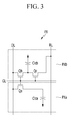
FIG. 3 is a circuit diagram of one pixel according to an exemplary embodiment of the present invention. -
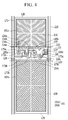
FIG. 4 is a plan layout of one pixel according to an exemplary embodiment of the present invention. -
FIG. 5 is a cross-sectional view taken along a line V-V ofFIG. 4 . -
FIG. 6 is a top plan view of a pixel according to an exemplary embodiment of the present invention. -
FIG. 7 is a graph illustrating generation of defective pixels in accordance with an inclusion ratio of ion inductors according to an exemplary embodiment of the present invention. - Hereinafter, exemplary embodiments of the present invention will be described in more detail with reference to the accompanying drawings. However, it is to be understood that exemplary embodiments of the present invention are not limited to the exemplary embodiments set forth herein. As those skilled in the art would realize, the exemplary embodiments may be modified in various different ways, all without departing from the scope of the present invention.
- In the specification and drawings, the thickness of layers, films, panels, or regions may be exaggerated for clarity. It will be understood that when an element such as a layer, film, region, or substrate is referred to as being "on" another element, it may be directly on the other element or intervening elements may also be present. Like reference numerals may designate like elements throughout the specification and drawings.
- In this specification, unless otherwise stated, when a target element is described as being "substituted", this may indicate that at least one hydrogen atom is substituted with a substituent selected from a set consisting of halogen atoms (F, Cl, Br, and I), a hydroxy group, a C1 to C20 alkoxy group, a nitro group, a cyano group, an amino group, an imino group, an azido group, an amidino group, a hydrazino group, a hydrazone group, a carbonyl group, a carbamoyl group, a thiol group, an ester group, an ether group, a carboxyl group or a salt thereof, a sulfonic acid group or a salt thereof, a phosphoric acid or a salt thereof, a C1 to C20 alkyl group, a C2 to C20 alkenyl group, a C2 to C20 alkynyl group, a C6 to C30 aryl group, a C3 to C20 cycloalkyl group, a C3 to C20 cycloalkenyl group, a C3 to C20 cycloalkynyl group, a C2 to C20 heterocycloalkyl group, a C2 to C20 heterocycloalkenyl group, a C2 to C20 heterocycloalkynyl group, a C3 to C30 heteroaryl group, or a combination thereof.
- In this specification, the prefix "hetero" may indicate that at least one heteroelement selected from a group consisting of at least one of N, O, S, and P are contained in a ring, unless otherwise stated.
- In this specification, unless otherwise stated, the term "alicyclic" may indicate a C3 to C40 cycloalkyl, a C3 to C40 cycloalkenyl, a C3 to C40 cycloalkynyl, a C3 to C40 cycloalkylene, a C3 to C40 cycloalkenylene, or a C3 to C40 cycloalkynylene. Specifically, this indicates a C3 to C20 cycloalkyl, a C3 to C20 cycloalkenyl, a C3 to C20 cycloalkynyl, a C3 to C20 cycloalkylene, a C3 to C20 cycloalkenylene, or a C3 to C20 cycloalkynylene. The term "aromatic" may indicate a C6 to C40 aryl, a C2 to C40 heteroaryl, a C6 to C40 arylene, or a C2 to C40 heteroarylene. For example, the term "aromatic" may indicate a C6 to C16 aryl, a C2 to C16 heteroaryl, a C6 to C16 arylene, or a C2 to C16 heteroarylene.
- Unless otherwise stated, the term "combination" may indicate a mixture or a copolymerization. For example, the term "combination" may indicate two or more rings being formed as a fused ring, or two or more rings being connected to each other by single bonding or a functional group such as -O-, -S-, -C(=O)-, -CH(OH)-, -S(=O)-, -S (=O)2-, -Si CH32-, - CH2p- (e.g." p = 1 or 2), - CF2q- (e.g., q = 1 or 2), -C CH32-, -C CF32-, -C CH3, and CF3- or -C(=O)NH-, in an alicyclic organic group and an aromatic organic group. Unless otherwise stated, the term "copolymerization" may indicate block copolymerization or random copolymerization, and the term "copolymer" may indicate a block copolymer or a random copolymer.
- Hereinafter, a liquid crystal display according to an exemplary embodiment of the present invention will be described in more detail with reference to
FIG. 1 andFIG. 2 .FIG. 1 is a perspective view of a liquid crystal display according to an exemplary embodiment of the present invention.FIG. 2 is a cross-sectional view partially illustrating constituent elements of a liquid crystal display according to an exemplary embodiment of the present invention. - Referring to
FIG. 1 , aliquid crystal display 10 according to an exemplary embodiment of the present invention may be a curved liquid crystal display. Theliquid crystal display 10 may be curved in a long axis direction (e.g., a horizontal direction), or may be curved in a short axis direction (e.g., a vertical direction). The curvedliquid crystal display 10 which may be curved in the long axis direction will be described in more detail below. However, exemplary embodiments of the present invention are not limited thereto. Exemplary embodiments of the present invention may include a flat-type display device. - Referring to
FIG. 2 , alower display panel 100 of theliquid crystal display 10 according to an exemplary embodiment of the present invention may include apixel electrode 191 disposed on afirst insulation substrate 110, and afirst alignment layer 11 disposed on thepixel electrode 191.Liquid crystal molecules 31 disposed adjacent to thefirst alignment layer 11 may have a pre-tilt angle. The pre-tilt refers to the obliqueness with respect to a direction substantially perpendicular to the surface of thefirst alignment layer 11 or thesecond alignment layer 21. - An
upper display panel 200 may include asecond insulation substrate 210 facing thefirst insulation substrate 110, acommon electrode 270 disposed on a surface of thesecond insulation substrate 210 facing the first insulation substrate, and asecond alignment layer 21 disposed on a surface of thecommon electrode 270 facing the first insulation substrate.Liquid crystal molecules 31 disposed adjacent to thesecond alignment layer 21 may have no pre-tilt angle, and may be aligned to be substantially perpendicular with respect to thesubstrate 210. Aliquid crystal layer 3 may be disposed between thelower display panel 100 and theupper display panel 200. - The
liquid crystal display 10 including thefirst alignment layer 11 and thesecond alignment layer 21 may reduce or prevent an occurrence of texture due to misalignment of theliquid crystal molecules 31 caused by theupper display panel 200 having no pre-tilt with respect to thelower display panel 100 and may control the reduction in transmittance, even when misalignment is generated between theupper display panel 200 and thelower display panel 100 due to the display device which is curved. - Hereinafter, the
first alignment layer 11 and thesecond alignment layer 21 will be described in more detail. The first and second alignment layers 11 and 21 may include different liquid crystal alignment agents, and may include a main chain and a side chain connected to the main chain. - The
first alignment layer 11 may include a first structural unit represented by Chemical Formula 1 and a second structural unit represented by Chemical Formula 2.


- According to an exemplary embodiment of the present invention, in Chemical Formulae 1 to 2, X1 and X2 are independently a tetravalent organic group derived from an alicyclic acid dianhydride or an aromatic acid dianhydride, and Y1 is a divalent organic group derived from an aromatic diamine. At least one hydrogen of the divalent organic group is substituted by Chemical Formula 1A. Y2 is a divalent organic group derived from an aromatic diamine, and at least one hydrogen of the divalent organic group is substituted by Chemical Formula 2A or Chemical Formula 2B.

- According to an exemplary embodiment of the present invention, in Chemical Formula 1A, R1 to R4 are independently hydrogen or a substituted or unsubstituted C1 to C8 alkyl group, and n is an integer that is in a range of 3 to 20. R5 is a substituted or unsubstituted C1 to C30 alkyl group. "a" and "b" are independently an integer between 0 to 4, and L1 and L2 are independently a single bond, -O-, -S (=O)2-, or -(C(Rx) (Ry))m-. Rx and Ry may each independently be a hydrogen atom or a substituted or unsubstituted C1 to C8 alkyl group, and m may be an integer that is in a range of 1 to 20.
- Y1 is a divalent organic group derived from the aromatic diamine. When at least one hydrogen of the divalent organic group is substituted by Chemical Formula 1A, Chemical Formula 1A may function like a vertical alignment group vertically aligning the
liquid crystal molecule 31 adjacent to the alignment layer.

- According to an exemplary embodiment of the present invention, in Chemical Formula 2A and Chemical Formula 2B, Cy is a C6 to C18 aryl group or a C6 to C18 cycloalkyl group, R11 to R14 are independently hydrogen or a substituted or unsubstituted C1 to C8 alkyl group, R15 and R16 are independently a hydroxyl group or a substituted or unsubstituted C1 to C8 alkoxy group, R17 is hydrogen, a hydroxyl group, or a substituted or unsubstituted C1 to C8 alkoxy group, "c" and "d" are independently integers between 0 to 4, k1 and k3 are an integer between 3 to 20, k2 is an integer between 0 to 5, Z1 and Z2 are independently -C(=O)-, and Z3 is -S- or -C(=O)-.
- The second structural unit represented by Chemical Formula 2 may include at least one of a benzophenone group, an acetophenone group, a benzoin ether group, and a benzyl group. The substituents may serve as radical anions to attract ion impurities, such as positive ion impurities, included in the
liquid crystal layer 3. - The second structural unit represented by Chemical Formula 2 may serve as a photo-reactive group or a photo-reactive derivative and may be reacted with a reactive mesogen (RM) included in the
liquid crystal layer 3. The reactive mesogen combined by the reaction may be coupled to thefirst alignment layer 11 as an alignment polymer, and thusliquid crystal molecules 31 disposed adjacent to thefirst alignment layer 11 may have a pre-tilt angle. - The
liquid crystal molecules 31 may be injected between thefirst insulation substrate 110 and thesecond insulation substrate 210. After theliquid crystal molecules 31 are injected between thefirst insulation substrate 110 and thesecond insulation substrate 210, if a voltage is applied and ultraviolet rays (UV) are radiated to theliquid crystal molecules 31, the substituent represented by Chemical Formula 2A or Chemical Formula 2B may generate a radical and may be reacted with the reactive mesogen in theliquid crystal layer 3 to be combined. That is, the reactive mesogen may be reacted with Chemical Formula 2A or 2B to be coupled to thefirst alignment layer 11 as the alignment polymer. - The
second alignment layer 21 may include the first structural unit represented by Chemical Formula 1 and a third structural unit represented byChemical Formula 3.

- According to an exemplary embodiment of the present invention, in
Chemical Formulae 1 and 3, X1 and X3 are independently a tetravalent organic group derived from an alicyclic acid dianhydride or an aromatic acid dianhydride, Y1 is a divalent organic group derived from an aromatic diamine, and at least one hydrogen of the divalent organic group is substituted by Chemical Formula 1A.
- According to an exemplary embodiment of the present invention, in Chemical Formula 1A, R1 to R4 are independently hydrogen or a substituted or unsubstituted C1 to C8 alkyl group, and n is an integer that is in a range of 3 to 20. R5 is a substituted or unsubstituted C1 to C30 alkyl group. "a" and "b" are independently integers that are in a range of 0 to 4, and L1 and L2 are independently a single bond, -O-, -S (=O)2-, or -(C(Rx) (Ry))m-. Rx and Ry are independently hydrogen atoms or a substituted or unsubstituted C1 to C8 alkyl group, and m is an integer that is in a range of 1 to 20.
- According to an exemplary embodiment of the present invention, in
Chemical Formula 3, Y3 is a divalent organic group derived from the aromatic diamine, and at least one hydrogen of the divalent organic group substituted by a substituted or unsubstituted C5 to C30 straight chain or a branched chain alkyl group (e.g., CH2 groups that are not adjacent to each other in the alkyl group may be substituted by -O-, -N(Ra)-, -C(=O)O-, -C(=O)N(Rb)-, -N(Rc)C(=O)-, or -OC(=O)-, and Ra, Rb, and Rc are independently hydrogen or a substituted or unsubstituted C1 to C8 alkyl group). - The third structural unit represented by
Chemical Formula 3 may include at least one of a pyridine group, a pyrimidine group, an indole group, a furan group, and a quinoline group. An electronegativity difference between carbon atoms and nitrogen atoms included in the substituent such as the pyridine group may generate a dipole moment in the substituent, and thesecond alignment layer 21 including the third structural unit represented byChemical Formula 3 may attract ion impurities, such as positive ion impurities, included in theliquid crystal layer 3. That is, the third structural unit represented byChemical Formula 3 may be an ion inductor. - The
second alignment layer 21 according to an exemplary embodiment of the present invention might not include the second structural unit represented by Chemical Formula 2 which serves as the photo-reactive group, and may vertically align theliquid crystal molecules 31 disposed adjacent to thesecond alignment layer 21 through the first structural unit represented by Chemical Formula 1 which has a vertical alignment function. That is, theliquid crystal molecules 31 disposed adjacent to thesecond alignment layer 21 might have no pre-tilt angle. - The liquid crystal alignment agent forming the
first alignment layer 11 and thesecond alignment layer 21 according to an exemplary embodiment of the present invention may include a polyimide. The polyimide may copolymerize at least one acid dianhydride selected from an alicyclic acid dianhydride, an aromatic acid dianhydride, and an aromatic diamine, to manufacture the polyamic acid and to be imidized. The manufacturing method of the polyamic acid is not limited to known methods used for the synthesis of the polyamic acid. - The alicyclic acid dianhydride may include at least one selected from 1,2,3,4-cyclobutanetetracarboxylic acid dianhydride (CBDA), 2,3,4,5-tetrahydrofurantetracarboxylic acid dianhydride, 5-(2,5-dioxotetrahydrofuryl)-3-methylcyclohexene-1,2-dicarboxylic acid anhydride (DOCDA), bicyclooctene-2,3,5,6-tetracarboxylic acid dianhydride (BODA), 1,2,3,4-cyclopentanetetracarboxylic acid dianhydride (CPDA), 1,2,4,5-cyclohexanetetracarboxylic acid dianhydride (CHDA), 1,2,4-tricarboxy-3-methylcarboxy cyclopentane dianhydride, 1,2,3,4-tetracarboxy cyclopentane dianhydride, 3,4-dicarboxy-1-cyclohexyl succinicacid dianhydride, 3,4-dicarboxy-1,2,3,4-tetrahydro-1-naphthalene succinic acid dianhydride, and 2,3,5-tricarboxycyclopentyl acetate acid dianhydride (2,3,5-tricarboxycyclopentyl acetic acid dianhydride, TCA-AH), but exemplary embodiments of the present invention are not limited thereto.
- The aromatic acid dianhydride may include at least one selected from pyromellitic acid dianhydride (PMDA), biphthalic acid anhydride (BPDA), oxydiphthalic acid dianhydride (ODPA), benzophenonetetracarboxylic acid dianhydride (BTDA), and hexafluoroisopropylidene diphthalic dianhydride (6-FDA), but exemplary embodiments of the present invention are not limited thereto.
- The liquid crystal alignment agent forming the
first alignment layer 11 and thesecond alignment layer 21 may include a solvent. By including the solvent, the liquid crystal alignment agent may have relatively high spreadability and adhesiveness with the substrate may be obtained. - Examples of the solvent according to exemplary embodiments of the present invention include N-methyl-2-pyrrolidone; N,N-dimethyl acetamide; N,N-dimethyl formamide; dimethyl sulfoxide; γ-butyrolactone; tetrahydrofuran(THF); and a phenol-based solvent such as meta-cresols, phenols, and halogenated phenols, but exemplary embodiments of the present invention are not limited thereto.
- The solvent may include 2-butyl cellosolve (2-BC), which may increase printability. The 2-butyl cellosolve may be included at 1 to about 50 wt% of the total content of the solvent including the 2-butyl cellosolve, and more specifically, may be included at about 10 to about 40 wt% of the total content of the solvent including the 2-butyl cellosolve. When the 2-butyl cellosolve is included in such a range, the printability may be increased.
- The solvent may include alcohol series, ketone series, ester series, ether series, hydrogen carbon series, or halogenated hydrogen carbon series as a poor solvent with a concentration in a range such in which a soluble polyimide polymer is not precipitated. The poor solvents may reduce a surface energy of the liquid crystal alignment agent, and may increase the spreadability and flatness of a coating.
- The poor solvent may be included at 1 to about 90 wt% of the total content of the solvent including the poor solvent, and more specifically, may be included at 1 to about 70 wt% of the total content of the solvent including the poor solvent.
- An example of the poor solvent according to an exemplary embodiment of the present invention may include one selected from methanol, ethanol, isopropanol, cyclohexanol, ethylene glycol, propylene glycol, 1,4-butanediol, triethylene glycol, acetone, methylethyl ketone, cyclo hexanone, methylacetate, ethylacetate, butyl acetate, diethyloxalate, malonate ester, diethylether, ethylene glycol monomethylether, ethylene glycol dimethylether, ethylene glycol monoethylether, ethylene glycol phenylether, ethylene glycol phenylmethylether, ethylene glycol phenylethylether, diethylene glycol dimethylether, diethyleneglycol ether, diethylene glycol monomethylether, diethylene glycol monoethylether, diethylene glycol monomethylether acetate, diethylene glycol monoethylether acetate, ethylene glycol methylether acetate, ethylene glycol ethylether acetate, 4-hydroxy-4-methyl-2-pentanone, 2-hydroxy ethyl propionate, 2-hydroxy-2-methyl ethyl propionate, ethoxy ethyl acetate, hydroxy ethyl acetate, 2-hydroxy-3-methyl methyl butanoate, 3-methoxy methyl propionate, 3-methoxy ethyl propionate, 3-ethoxy ethyl propionate, 3-ethoxy methyl propionate, methyl methoxy butanol, ethyl methoxy butanol, methyl ethoxy butanol, ethyl ethoxy butanol, tetrahydrofuran, dichloromethane, 1,2-dichloroethane, 1,4-dichloro butane, trichloroethane, chlorobenzene, o-dichlorobenzene, hexane, heptane, octane, benzene, toluene, xylene, and combinations thereof.
- The liquid crystal alignment agent for forming the
first alignment layer 11 and thesecond alignment layer 21 may include other additives. - The other additives may include an epoxy compound. The epoxy compound may be used to increase the reliability and an electro-optical characteristic. The epoxy compound may include at least one epoxy compound including 2 to 8 epoxy groups, and more specifically, 2 to 4 epoxy groups.
- The epoxy compound may be included at 0.1 to about 50 parts by weight of the polyimide, and more specifically, may be included at 1 to about 30 parts by weight of the polyimide. When the epoxy compound is included in the above range, while showing printability and flatness on the coating on the substrate, the reliability and the electro-optical characteristic may be increased.
- Specific examples of the epoxy compound according to an exemplary embodiment of the present invention include N,N,N',N'-tetraglycidyl-4,4'-diaminophenylmethane (TGDDM), N,N,N',N'-tetraglycidyl-4,4'-diaminophenylethane, N,N,N',N'-tetraglycidyl-4,4'-diaminophenylpropane, N,N,N',N'-tetraglycidyl-4,4'-diaminophenylbutane, N,N,N',N'-tetraglycidyl-4,4'-diaminobenzene, ethyleneglycolglycidylether, polyethyleneglycolglycidylether, propyleneglycolglycidylether, tripropyleneglycolglycidylether, polypropyleneglycolglycidylether, neopentylglycolglycidylether, 1,6-hexane dioldiglycidylether, glycerin diglycidylether, 2,2-dibromoneopentylglycolglycidylether, 1,3,5,6-tetraglycidyl-2,4-hexane diol, N,N,N',N'-tetraglycidyl-1,4-phenylene diamine, N,N,N',N'-tetraglycidyl-m-xylene diamine, N,N,N',N'-tetraglycidyl-2,2'-dimethyl-4,4'-diaminobiphenyl, 2,2-bis[4-(N,N-diglycidyl-4-aminophenoxy)phenyl]propane, N,N,N',N'-tetraglycidyl-4,4'-diaminodi phenylmethane, 1,3-bis(N,N-diglycidylaminomethyl)cyclohexane, and 1,3-bis(N,N-diglycidylaminomethyl)benzene, but exemplary embodiments of the present invention are not limited thereto.
- To increase the printability, a surfactant or a coupling agent may be included in the liquid crystal alignment agent.
- The first and second liquid crystal alignment layers 11 and 21 may be formed by coating the liquid crystal alignment agent on the substrate. A method of coating the liquid crystal alignment agent on the substrate may include a spin coating method, a flexo printing method, and an inkjet method. The flexo printing method may provide relatively high uniformity of the coated layer and a relatively large sized coating layer may be formed.
- To increase the uniformity of the coated layer, after the liquid crystal alignment agent is uniformly coated on the substrate, pre-drying may be performed at a temperature from room temperature to about 200°C, and more specifically, at a temperature of from about 30°C to about 150°C, and even more specifically, at a temperature of from about 40°C to about 120°C, for a duration of 1 minute to about 100 minutes. Through the pre-drying, by adjusting the volatility of each component of the liquid crystal alignment agent, a uniformly coated layer without a deviation may be obtained.
- Next, firing may be performed at a temperature of from about 80°C to about 300°C, specifically at a temperature of from about 120°C to about 280°C, for a duration of about 5 minutes to about 300 minutes to evaporate the solvent. Thus, the alignment layers 11 and 21 may be formed.
- The
first alignment layer 11 may include the vertical alignment group (e.g., the vertical alignment group included in the first structural unit represented by Chemical Formula 1 as the side chain) and the photo-reactive group (e.g., the photo reactive group included in the second structural unit represented by Chemical Formula 2 as the side chain), and theliquid crystal molecules 31 adjacent to the first alignment layer may have the pre-tilt angle due to the alignment polymer in which the photo-reactive group and the reactive mesogen are combined according to the manufacturing process according to an exemplary embodiment of the present invention. - The
second alignment layer 21 may include the vertical alignment group (e.g., the vertical alignment group included in the first structural unit represented by Chemical Formula 1 as the side chain) and the ion inductor (e.g., the ion inductor included in the third structural unit represented byChemical Formula 3 as the side chain), and thusliquid crystal molecules 31 disposed adjacent to thesecond alignment layer 21 may be vertically aligned by the vertical alignment group. - In accordance with the liquid crystal display including
liquid crystal molecules 31 of which the pre-tilt angle is changed according to thefirst alignment layer 11 and the second alignment layer 12, although the upper andlower display panels liquid crystal molecules 31 adjacent to thefirst alignment layer 11 and theliquid crystal molecules 31 adjacent to thesecond alignment layer 21 may be reduced or prevented Thus, an occurrence of the texture generation may be reduced or prevented. - The liquid crystal display according to an exemplary embodiment of the present invention may include the first and second alignment layers 11 and 21 including a substituent such as the benzophenone group included in the second structural unit represented by Chemical Formula 2 of the
first alignment layer 11 and a substituent such as the pyridine group included in the third structural unit represented byChemical Formula 3 of thesecond alignment layer 21 for attracting ion impurities included in theliquid crystal layer 3. - Accordingly, an occurrence of afterimages may be reduced or prevented and the display quality may be increased by preventing ion impurities from being accumulated in a side of the
first alignment layer 11 or thesecond alignment layer 21. - The
first alignment layer 11 according to an exemplary embodiment of the present invention may include the third structural unit represented byChemical Formula 3. That is, thefirst alignment layer 11 may include an ion inductor. - The
first alignment layer 11 according to an exemplary embodiment of the present invention may include the first structural unit represented by Chemical Formula 1, the second structural unit represented by Chemical Formula 2, and the third structural unit represented byChemical Formula 3. Accordingly, thefirst alignment layer 11 may include the vertical alignment group, the photo-reactive group or the photo-reactive derivative, and the ion inductor. - The
second alignment layer 21 according to an exemplary embodiment of the present invention may be substantially the same as thesecond alignment layer 21 according to the exemplary embodiments of the present invention described above. - According to an exemplary embodiment of the present invention, both of the
first alignment layer 11 and thesecond alignment layer 21 may include the ion inductor, and thus the ion impurities included in theliquid crystal layer 3 may be guided to theupper display panel 200 and thelower display panel 100. Accordingly, an occurrence of afterimages due to the ion impurities accumulated at a side of the liquid crystal display may be reduced or prevented. - According to a manufacturing process of the display device according to an exemplary embodiment of the present invention, when a laser irradiates some pixels with light, halogen ions or radicals may be generated at color filters. These impurities such as the halogen ions or the radicals may be coupled to the ion inductor included in the first and second alignment layers 11 and 21, and thus the alignment layers 11 and 21 according to an exemplary embodiment of the present invention may control defective pixels generated due to the halogen ions or the radicals.
- Hereinafter, a liquid crystal display according to an exemplary embodiment of the present invention will be described in more detail with reference to
FIG. 3 to FIG. 6 .FIG. 3 is a circuit diagram of one pixel according to an exemplary embodiment of the present invention.FIG. 4 is a plan layout of one pixel according to an exemplary embodiment of the present invention.FIG. 5 is a cross-sectional view taken along a line V-V ofFIG. 4 .FIG. 6 is a top plan view of a pixel according to an exemplary embodiment of the present invention. - Referring to
FIG. 3 , one pixel PX (e.g., the pixel PX including a first sub-pixel electrode PXa and a second sub-pixel electrode PXb) of the liquid crystal display according to an exemplary embodiment of the present invention may include a plurality of signal lines including a gate line GL transferring a gate signal, a data line DL transferring a data signal, and a divided reference voltage line RL transferring a divided voltage reference voltage. The one pixel PX may include first, second, and third switching elements Qa, Qb, and Qc, and first and second liquid crystal capacitors Clca and Clcb connected to the plurality of signal lines. - The first and second switching elements Qa and Qb may be connected to the gate line GL and the data line DL, respectively, and the third switching element Qc may be connected to an output terminal of the second switching element Qb and the divided reference voltage line RL.
- The first switching element Qa and the second switching element Qb may each be three-terminal elements such as a thin film transistor. A control terminal is connected to the gate line GL, an input terminal of each of the first switching element Qa and the second switching element Qb may be connected to the data line DL, an output terminal of the first switching element Qa may be connected to the first liquid crystal capacitor Clca, and the output terminal of the second switching element Qb may be connected to the second liquid crystal capacitor Clcb and an input terminal of the third switching element Qc.
- The third switching element Qc may be the three-terminal element such as the thin film transistor. The control terminal of the third switching element Qc may be connected to the gate line GL. The input terminal of the third switching element Qc may be connected to the second liquid crystal capacitor Clcb, and an output terminal of the third switching element Qc may be connected to the divided reference voltage line RL.
- If a gate-on signal is applied to the gate line GL, the first switching element Qa, the second switching element Qb, and the third switching element Qc connected to the gale line GL may be turned on. Accordingly, the data voltage applied to the data line DL may be applied to the first sub-pixel electrode Pxa and the second sub-pixel electrode PXb through the first switching element Qa and the second switching element Qb that are turned on. The data voltages applied to the first sub-pixel electrode PXa and the second sub-pixel electrode PXb may be the same as each other, and the first liquid crystal capacitor Clca and the second liquid crystal capacitor Clcb may be charged by the same value as a difference between the common voltage and the data voltage. Substantially simultaneously, the voltage charged in the second liquid crystal capacitor Clcb may be divided through the turned-on third switching element Qc. Accordingly, a value of the voltage charged in the second liquid crystal capacitor Clcb may be reduced by a difference between the common voltage and the divided voltage reference voltage. That is, the voltage charged in the first liquid crystal capacitor Clca may become higher than the voltage charged in the second liquid crystal capacitor Clcb.
- Accordingly, the voltage charged in the first liquid crystal capacitor Clca may be different from the voltage charged in the second liquid crystal capacitor Clcb. Since the voltage of the first liquid crystal capacitor Clca and the voltage of the second liquid crystal capacitor Clcb may be different from each other, inclination angles of
liquid crystal molecules 31 in a first sub-pixel and a second sub-pixel become different from each other, and thus luminances of the two sub-pixels become different from each other. Accordingly, if the voltage of the first liquid crystal capacitor Clca and the voltage of the second liquid crystal capacitor Clcb are adjusted, an image viewed in a lateral surface may be substantially the same as an image viewed in a front, and thus lateral surface visibility may be increased. - According to an exemplary embodiment of the present invention, to make the voltage charged in the first liquid crystal capacitor Clca and the voltage charged in the second liquid crystal capacitor Clcb different, the third switching element Qc connected to the second liquid crystal capacitor Clcb and the divided reference voltage line RL may be included. In the liquid crystal display according to another exemplary embodiment of the present invention, the second liquid crystal capacitor Clcb may be connected to a step-down capacitor.
- The third switching element including a first terminal connected to a step-down gate line, a second terminal connected to the second liquid crystal capacitor Clcb, and a third terminal connected to a step-down capacitor may charge a portion of an amount of electric charges charged in the second liquid crystal capacitor Clcb in the step-down capacitor, and thus charge voltages between the first liquid crystal capacitor Clca and the second liquid crystal capacitor Clcb may be set to be different from each other. In the liquid crystal display according to an exemplary embodiment of the present invention, the first liquid crystal capacitor Clca and the second liquid crystal capacitor Clcb may be connected to different data lines to receive different data voltages, and thus charge voltages between the first liquid crystal capacitor Clca and the second liquid crystal capacitor Clcb may be set to be different from each other. The charge voltages between the first liquid crystal capacitor Clca and the second liquid crystal capacitor Clcb may be set to be different from each other by various methods.
- First, referring to
FIG. 4 andFIG. 5 , the liquid crystal display according to an exemplary embodiment of the present invention may include alower display panel 100 and anupper display panel 200 facing each other. Aliquid crystal layer 3 may be disposed between the twodisplay panels display panels - The
lower display panel 100 will be described below in more detail. - A gate conductor including a
gate line 121 and a dividedreference voltage line 131 may be disposed on an insulatingsubstrate 110. The insulatingsubstrate 110 may include transparent glass or plastics. - The
gate line 121 may include afirst gate electrode 124a, asecond gate electrode 124b, athird gate electrode 124c, and a wide end portion which may connect to another layer or an external driving circuit. - The divided
reference voltage line 131 may includefirst storage electrodes reference electrode 137.Second storage electrodes reference voltage line 131 but overlap a secondsub-pixel electrode 191b. - A
gate insulating layer 140 may be disposed on thegate line 121 and the dividedreference voltage line 131. - A
first semiconductor layer 154a, asecond semiconductor layer 154b, and athird semiconductor layer 154c may be disposed on thegate insulating layer 140. A plurality ofohmic contacts semiconductor layers - A plurality of
data lines 171 including afirst source electrode 173a and asecond source electrode 173b, and data conductors including afirst drain electrode 175a, asecond drain electrode 175b, athird source electrode 173c, and athird drain electrode 175c may be disposed on theohmic contacts gate insulating layer 140. - The data conductors, the semiconductors disposed under the data conductors, and the ohmic contacts may be simultaneously formed using a single mask.
- The
data line 171 may include a wide end portion which may connect to another layer or an external driving circuit. - The
first gate electrode 124a, thefirst source electrode 173a, and thefirst drain electrode 175a may form the first thin film transistor Qa along with thefirst semiconductor layer 154a, and a channel of the first thin film transistor Qa may be disposed at thefirst semiconductor layer 154a between thefirst source electrode 173a and thefirst drain electrode 175a. Similarly, thesecond gate electrode 124b, thesecond source electrode 173b, and thesecond drain electrode 175b may form the second thin film transistor Qb along with thesecond semiconductor layer 154b, and a channel of the second thin film transistor Qb may be disposed at thesecond semiconductor layer 154b between thesecond source electrode 173b and thesecond drain electrode 175b. Thethird gate electrode 124c, thethird source electrode 173c, and thethird drain electrode 175c may form the third thin film transistor Qc along with thethird semiconductor layer 154c, and a channel of the third thin film transistor Qc may be disposed at thethird semiconductor layer 154c between thethird source electrode 173c and thethird drain electrode 175c. - The
second drain electrode 175b may be connected to thethird source electrode 173c and may be connected to the pixel electrode through awide expansion 177. - A
first passivation layer 180p may be disposed on thedata conductors semiconductors layers first passivation layer 180p may include an inorganic insulating layer including a silicon nitride or a silicon oxide. Thefirst passivation layer 180p may reduce or prevent a pigment of acolor filter 230 from flowing into the exposedsemiconductor layers - The
color filter 230 may be disposed on thefirst passivation layer 180p. Thecolor filter 230 may extend in a vertical direction along two adjacent data lines. Alight blocking member 220 may be disposed on thefirst passivation layer 180p, an edge of thecolor filter 230, and thedata line 171. - The
light blocking member 220 may extend along thedata line 171, and may be disposed between two adjacent color filters 230. A width of thelight blocking member 220 may be wider than a width of thedata line 171. The width of thelight blocking member 220 may be wider than the width of thedata line 171. Thelight blocking member 220 may reduce or prevent light incident from the outside from being reflected from a surface of thedata line 171, which may be a metal data line. Light reflected from the surface of thedata line 171 may interfere with light passing through theliquid crystal layer 3, which may reduce or prevent a contrast ratio of the liquid crystal display from being decreased. Exemplary embodiments of the present invention are described in which thelight blocking member 220 is disposed in exemplary locations, however exemplary embodiments of the present invention are not limited thereto, and a shielding electrode (not shown) which may be disposed in the same layer as the pixel electrode may replace thelight blocking member 220. - The
light blocking member 220 may cover the first transistor Qa, the second transistor Qb, and the third transistor Qc, and may extend in the same direction as thegate line 121 to overlap a portion of thedata line 171. Thelight blocking member 220 may overlap at least a portion of twodata lines 171 disposed at both sides of one pixel area to prevent light leakage generated near thedata line 171 and thegate line 121. Light leakage may be reduced or prevented in the region where the first transistor Qa, the second transistor Qb, and the third transistor Qc are disposed. - A
second passivation layer 180q may be disposed on thecolor filter 230 and thelight blocking member 220. - The
second passivation layer 180q may include an inorganic insulating layer that is formed of a silicon nitride or a silicon oxide. Thesecond passivation layer 180q may reduce or prevent peeling of thecolor filter 230, and may reduce or prevent contamination of theliquid crystal layer 3 by an organic material such as a solvent flowing from thecolor filter 230 and may reduce or prevent defects such as afterimages that may occur when an image is driven. - One of the
first passivation layer 180p and thesecond passivation layer 180q may be omitted. - A
first contact hole 185a and asecond contact hole 185b may be disposed in the first and second passivation layers 180p and 180q to expose the first andsecond drain electrodes - A
third contact hole 185c may be disposed in thefirst passivation layer 180p, thesecond passivation layer 180q, and thegate insulating layer 140 to partially expose thereference electrode 137 and thethird drain electrode 175c. Thethird contact hole 185c may be covered with a connectingmember 195. The connectingmember 195 may electrically connect thereference electrode 137 and thethird drain electrode 175c that are exposed through thethird contact hole 185c. - A plurality of
pixel electrodes 191 may be disposed on thesecond passivation layer 180q. Eachpixel electrode 191 may include afirst subpixel electrode 191a and asecond subpixel electrode 191b which may be separated from each other. Thegate line 121 may be disposed between thepixel electrodes 191. Thepixel electrodes 191 may be adjacent in a column direction based on thegate line 121. - The
pixel electrode 191 may include a transparent material such as ITO or IZO. Thepixel electrode 191 may include a transparent conductive material such as ITO or IZO, or a reflective metal such as aluminum, silver, chromium, or an alloy thereof. - Each of the
first subpixel electrode 191a and thesecond subpixel electrode 191b may include one or morebasic electrode 199 illustrated inFIG. 6 , or a modification of thebasic electrode 199. - The
first sub-pixel electrode 191a and the secondsub-pixel electrode 191b may be physically and electrically connected through thefirst contact hole 185a and thesecond contact hole 185b to thefirst drain electrode 175a and thesecond drain electrode 175b, respectively. Thefirst sub-pixel electrode 191a and the secondsub-pixel electrode 191b may receive a data voltage from thefirst drain electrode 175a and thesecond drain electrode 175b. Some of the data voltage applied to thesecond drain electrode 175b may be divided through thethird source electrode 173c, and thus a size of the voltage applied to thefirst subpixel electrode 191a may be larger than that of the voltage applied to thesecond subpixel electrode 191b. - The
first subpixel electrode 191a and the secondsub-pixel electrode 191b to which the data voltage is applied may generate an electric field together with acommon electrode 270 of theupper display panel 200 to determine a direction of theliquid crystal molecules 31 of theliquid crystal layer 3 between thepixel electrode 191 and thecommon electrode 270. The luminance of light passing through theliquid crystal layer 3 may be changed according to the direction of theliquid crystal molecules 31. - The
first passivation layer 180p, thecolor filter 230, and thesecond passivation layer 180q may be disposed in the region where the first transistor Qa, the second transistor Qb, the third transistor Qc, and the first tothird contact holes third contact holes - The
first alignment layer 11 may be disposed on thepixel electrode 191. Thefirst alignment layer 11 may be substantially the same as thefirst alignment layer 11 according to the above-described exemplary embodiment of the present invention. - The
first alignment layer 11 may include the reactive mesogen (RM) combined by the UV radiation. That is, the reactive mesogen included in theliquid crystal layer 3 may be combined with the photo-reactive group by the UV radiation to form the alignment polymer. The reactive mesogen included in thefirst alignment layer 11 may pre-tilt theliquid crystal molecules 31 disposed adjacent to thefirst alignment layer 11. - The
liquid crystal layer 3 may have a negative dielectric anisotropy, andliquid crystal molecules 31 of theliquid crystal layer 3 may be vertically aligned with respect to the surface of the twodisplay panels - The
liquid crystal layer 3 may include the reactive mesogen. When the reactive mesogen is included in thefirst alignment layer 11 by UV radiation, a relatively small amount of the reactive mesogen may remain in theliquid crystal layer 3. - The
upper display panel 200 will be described below in more detail. - The
common electrode 270 may be disposed on a surface of thesecond insulation substrate 210, which the surface of thesecond insulation substrate 210 faces the first insulation substrate, and thesecond alignment layer 21 may be disposed on a surface of thecommon electrode 270 which the surface of thecommon electrode 270 faces the first insulation substrate. Thesecond alignment layer 21 may include a same material as thesecond alignment layer 21 according to the exemplary embodiments of the present invention, and theliquid crystal molecules 31 adjacent to thesecond alignment layer 21 may be vertically aligned. - The
basic electrode 199 will be described in more detail with reference toFIG. 6 . - As shown in
FIG. 6 , thebasic electrode 199 may have a quadrangular shape. Thebasic electrode 199 may include a cross-shaped stem including ahorizontal stem 193 and avertical stem 192 perpendicular to thehorizontal stem 193. Thebasic electrode 199 may be divided into a first subregion Da, a second subregion Db, a third subregion Dc, and a fourth subregion Dd by thehorizontal stem 193 and thevertical stem 192. Each subregion Da-Dd may include a plurality offirst minute branches 194a, a plurality ofsecond minute branches 194b, a plurality ofthird minute branches 194c and a plurality offourth minute branches 194d. - The
first minute branch 194a may obliquely extend from thetransverse stem 193 or thelongitudinal stem 192 in the upper-left direction. Thesecond minute branch 194b may obliquely extend from thetransverse stem 193 or thelongitudinal stem 192 in the upper-right direction. Thethird minute branch 194c may obliquely extend from thetransverse stem 193 or thelongitudinal stem 192 in the lower-left direction. Thefourth minute branch 194d may obliquely extend from thetransverse stem 193 or thelongitudinal stem 192 in the lower-right direction. - The first to
fourth minute branches horizontal stem 193. Theminute branches - Widths of the
minute branches adjacent minute branches - According to another exemplary embodiment of the present invention, the widths of the
minute branches horizontal stem portion 193 or thevertical stem portion 192, and a difference between the largest width portion and the narrowest portion in oneminute branch - The
first sub-pixel electrode 191a and the secondsub-pixel electrode 191b may be connected through thefirst contact hole 185a and thesecond contact hole 185b to thefirst drain electrode 175a and thesecond drain electrode 175b, respectively, and may receive a data voltage from thefirst drain electrode 175a and thesecond drain electrode 175b. In this case, sides of the first tofourth minute branches liquid crystal molecules 31. The horizontal components of the electric field may be substantially horizontal with respect to the sides of the first tofourth minute branches FIG. 1 , theliquid crystal molecules 31 may be inclined in a direction that is parallel to longitudinal directions of theminute branches pixel electrode 191 may include the four subregions Da-Dd in which longitudinal directions of theminute branches liquid crystal molecules 31 may be inclined in four directions such that four domains having different alignment directions of theliquid crystal molecules 31 may be formed in theliquid crystal layer 3. As described above, when the inclination directions of the liquid crystal molecules are diversified, a reference viewing angle of the liquid crystal display may be increased. - Hereinafter, a generation of defective pixels due to the alignment layers according to an exemplary embodiment of the present invention will be described in more detail with reference to
FIG. 7 . -
FIG. 7 is a graph illustrating generation of defective pixels in accordance with an inclusion ratio of ion inductors according to an exemplary embodiment of the present invention. - Referring to
FIG. 7 , according to an exemplary embodiment of the present invention, the number of defective pixels that is generated may be reduced or eliminated as a content of ion inductors included in the alignment layers (e.g. the first and second alignment layers 11 and 21) is increased. The ion inductors may be combined with halogen ions or radicals that cause the defect of pixels which may reduce or eliminate the generation of defective pixels. - According to an exemplary embodiment of the present invention, a difference of the voltages generated according to whether or not the inductors exist may be about 30 mV. This may indicate the reduction of afterimages formed due to charges accumulated at the
second alignment layer 21 including the ion inductors. - In the liquid crystal display according to exemplary embodiments of the present invention, the liquid crystal molecules disposed adjacent to the first alignment layer may be pre-tilted, while the liquid crystal molecules disposed adjacent to the second alignment layer may be vertically arranged without being pretiled. Accordingly, even when the upper and lower display panels are misaligned due to being curved, there may be no alignment generated in the liquid crystal molecules, thus reducing or preventing a reduction in display quality and/or transmittance of the display device according to exemplary embodiments of the present invention.
- Each alignment layer disposed in the upper and lower display panels may have a polarity to uniformly move ion impurities in the liquid crystal layer to the upper and lower display panels, thereby reducing or preventing a reduction in display quality due to charge accumulation.
While the present invention has been shown and described with reference to the exemplary embodiments thereof, it will be apparent to those of ordinary skill in the art that various changes in form and detail may be made thereto without departing from the scope of the present invention.
Claims (15)
- A liquid crystal display (10) comprising:a first insulation substrate (110);a pixel electrode (191) disposed on the first insulation substrate (110);a first alignment layer (11) disposed on the pixel electrode (191);a second insulation substrate (210) facing the first insulation substrate (110);a common electrode (270) disposed on a surface of the second insulation substrate (210), the surface of the second insulation substrate (210) facing the first insulation substrate (110);a second alignment (21) layer disposed on a surface of the common electrode (270), the surface of the common electrode (270) facing the first insulation substrate (110); anda liquid crystal layer (3) disposed between the first alignment layer (11) and the second alignment layer (21), wherein the liquid crystal layer (3) includes liquid crystal molecules (31),wherein liquid crystal molecules (31) adjacent to at least one of the first alignment layer (11) and the second alignment layer (21) have a pre-tilt angle, andwherein at least one of the first alignment layer (11) and the second alignment layer (21) has an ion inductor.
- The liquid crystal display (10) of claim 1, wherein the first alignment layer (11) and the second alignment layer (21) each include a main chain and a side chain connected to the main chain and at least one of the side chains of the first alignment layer (11) and the second alignment layer (21) includes a photo-reactive group or a photo-reactive derivative.
- The liquid crystal display (10) of claim 2, wherein the side chain of the first alignment layer (11) includes the photo-reactive group or the photo-reactive derivative.
- The liquid crystal display (10) of one of claims 2 or 3, wherein the photo-reactive group or the photo-reactive derivative includes at least one of a benzophenone group, an acetophenone group, a benzoin ethers group, and a benzyl group.
- The liquid crystal display (10) of one of claims 1 to 4, wherein the at least one side chain of the second alignment layer (21) is free of a photo-reactive group or the photo-reactive derivative.
- The liquid crystal display (10) of one of claims 2 to 5, wherein the side chain of the second alignment layer (21) includes an ion inductor and the ion inductor includes at least one of a pyridine group, a pyrimidine group, an indole group, a furan group, and a quinoline group.
- The liquid crystal display (10) of one of claims 2 to 6, wherein at least one of the side chains of the first alignment layer (11) and the second alignment layer (21) includes a vertical alignment group.
- The liquid crystal display (10) of one of claims 1 to 7, wherein the first alignment layer (11) and the second alignment layer (21) include different materials from each other.
- The liquid crystal display (10) of one of claims 1 to 8, wherein the liquid crystal molecules (31) near the first alignment layer (11) are pre-tilted and the liquid crystal molecules (31) positioned near the second alignment layer (21) are at least substantially perpendicular with respect to the second insulation substrate (210).
- The liquid crystal display (10) of one of claims 1 to 9, wherein the liquid crystal display (10) is a curved-type of liquid crystal display (10).
- The liquid crystal display (10) of one of claims 1 to 10, wherein the liquid crystal layer (3) has negative dielectric anisotropy and wherein the liquid crystal layer (3) further includes a reactive mesogen (RM).
- The liquid crystal display (10) of claim 11, wherein one of the first alignment layer (11) and the second alignment layer (21) includes an alignment polymer, and wherein the reactive mesogen and the photo-reactive group or a photo-reactive derivative are coupled to the alignment polymer.
- The liquid crystal display (10) of one of claims 1 to 12, wherein one of the first alignment layer (11) and the second alignment layer (21) includes a first structural unit represented by Chemical Formula 1:


- The liquid crystal display (10) of one of claims 1 to 13, wherein the first alignment layer (11) includes a second structural unit represented by Chemical Formula 2:


- The liquid crystal display (10) of one of claims 1 to 14, wherein one of the first alignment layer (11) and the second alignment layer (21) includes a third structural unit represented by Chemical Formula 3:

Applications Claiming Priority (1)
| Application Number | Priority Date | Filing Date | Title |
|---|---|---|---|
| KR1020150038459A KR20160113423A (en) | 2015-03-19 | 2015-03-19 | Liquid crystal display device |
Publications (2)
| Publication Number | Publication Date |
|---|---|
| EP3070517A1 true EP3070517A1 (en) | 2016-09-21 |
| EP3070517B1 EP3070517B1 (en) | 2020-05-06 |
Family
ID=55436013
Family Applications (1)
| Application Number | Title | Priority Date | Filing Date |
|---|---|---|---|
| EP16156903.3A Not-in-force EP3070517B1 (en) | 2015-03-19 | 2016-02-23 | Liquid crystal display device having polymer alignment layers with side chains including ion-attracting groups |
Country Status (4)
| Country | Link |
|---|---|
| US (1) | US10338435B2 (en) |
| EP (1) | EP3070517B1 (en) |
| KR (1) | KR20160113423A (en) |
| CN (1) | CN105988247A (en) |
Families Citing this family (2)
| Publication number | Priority date | Publication date | Assignee | Title |
|---|---|---|---|---|
| KR102537443B1 (en) * | 2018-04-03 | 2023-05-30 | 삼성디스플레이 주식회사 | Liquid crystal display apparatus |
| DE102023110269B3 (en) * | 2023-04-21 | 2023-12-28 | Sioptica Gmbh | Switchable light filter, lighting device and screen |
Citations (3)
| Publication number | Priority date | Publication date | Assignee | Title |
|---|---|---|---|---|
| EP2330458A1 (en) * | 2008-09-03 | 2011-06-08 | Sharp Kabushiki Kaisha | Alignment film, alignment film material, liquid crystal display device comprising alignment film, and method for manufacturing same |
| WO2013156053A1 (en) * | 2012-04-16 | 2013-10-24 | Lachezar Komitov | Polymer for use in alignment layer |
| EP2843466A1 (en) * | 2013-08-28 | 2015-03-04 | InnoLux Corporation | Light leakage reduction in vertically-aligned liquid crystal displays using polymeric particles formed on an alignment layer |
Family Cites Families (13)
| Publication number | Priority date | Publication date | Assignee | Title |
|---|---|---|---|---|
| JP2004151546A (en) * | 2002-10-31 | 2004-05-27 | Sharp Corp | Active matrix substrate and display device |
| JP2006085098A (en) | 2004-09-17 | 2006-03-30 | Fuji Photo Film Co Ltd | Alignment layer, optical compensation sheet and liquid crystal display device |
| US8514357B2 (en) | 2008-09-17 | 2013-08-20 | Samsung Display Co., Ltd. | Alignment material, alignment layer, liquid crystal display device and manufacturing method thereof |
| KR101613629B1 (en) | 2009-01-19 | 2016-04-20 | 삼성디스플레이 주식회사 | Liquid crystal display device, method of manufacturing the same and alignment layer composition |
| JP5630013B2 (en) | 2009-01-30 | 2014-11-26 | ソニー株式会社 | Manufacturing method of liquid crystal display device |
| JP2012032752A (en) * | 2009-12-09 | 2012-02-16 | Sony Corp | Liquid crystal display element and liquid crystal display device |
| TWI411985B (en) * | 2010-03-22 | 2013-10-11 | Au Optronics Corp | Curved display panel |
| KR20120088010A (en) | 2010-09-13 | 2012-08-08 | 삼성전자주식회사 | Liquid crystal display and method for manufacturing the same |
| KR101806351B1 (en) | 2011-02-01 | 2018-01-11 | 삼성디스플레이 주식회사 | Vertical alignment layer and liquid crystal display including the same |
| US9249355B2 (en) * | 2011-02-05 | 2016-02-02 | Merck Patent Gmbh | Liquid-crystal displays having homeotropic alignment |
| JP5741055B2 (en) | 2011-02-25 | 2015-07-01 | ソニー株式会社 | Liquid crystal display device and manufacturing method thereof |
| WO2012133819A1 (en) | 2011-03-31 | 2012-10-04 | 日産化学工業株式会社 | Liquid crystal aligning agent , liquid crystal alignment film, liquid crystal display element, process for producing liquid crystal display element, and polymerizable compound |
| KR102069822B1 (en) | 2013-07-24 | 2020-01-28 | 삼성디스플레이 주식회사 | Liquid crystal display and manufacturing method thereof |
-
2015
- 2015-03-19 KR KR1020150038459A patent/KR20160113423A/en not_active Ceased
- 2015-11-18 US US14/945,026 patent/US10338435B2/en active Active
-
2016
- 2016-02-23 EP EP16156903.3A patent/EP3070517B1/en not_active Not-in-force
- 2016-03-16 CN CN201610150898.XA patent/CN105988247A/en active Pending
Patent Citations (3)
| Publication number | Priority date | Publication date | Assignee | Title |
|---|---|---|---|---|
| EP2330458A1 (en) * | 2008-09-03 | 2011-06-08 | Sharp Kabushiki Kaisha | Alignment film, alignment film material, liquid crystal display device comprising alignment film, and method for manufacturing same |
| WO2013156053A1 (en) * | 2012-04-16 | 2013-10-24 | Lachezar Komitov | Polymer for use in alignment layer |
| EP2843466A1 (en) * | 2013-08-28 | 2015-03-04 | InnoLux Corporation | Light leakage reduction in vertically-aligned liquid crystal displays using polymeric particles formed on an alignment layer |
Also Published As
| Publication number | Publication date |
|---|---|
| US20160274417A1 (en) | 2016-09-22 |
| KR20160113423A (en) | 2016-09-29 |
| CN105988247A (en) | 2016-10-05 |
| EP3070517B1 (en) | 2020-05-06 |
| US10338435B2 (en) | 2019-07-02 |
Similar Documents
| Publication | Publication Date | Title |
|---|---|---|
| KR100913605B1 (en) | Liquid crystal photo-alignment agent, liquid crystal photo-alignment layer comprising the same, and liquid crystal display device comprising the same | |
| KR102069822B1 (en) | Liquid crystal display and manufacturing method thereof | |
| TWI531596B (en) | Photo-alignment agent of liquid crystal, photo-alignment film of liquid crystal including the agent, and liquid crystal display including the film | |
| US8580357B2 (en) | Liquid crystal display device | |
| KR101056424B1 (en) | Liquid crystal photo-alignment agent, liquid crystal photo-alignment layer comprising the same, and liquid crystal display device comprising the same | |
| US9709852B2 (en) | Curved liquid crystal display and method of manufacturing the same | |
| JP2007094406A (en) | Liquid crystal display | |
| KR101387735B1 (en) | Liquid crystal alignment agent, liquid crystal alignment film using the same, and liquid crystal display device including the liquid crystal alignment film | |
| EP3070517B1 (en) | Liquid crystal display device having polymer alignment layers with side chains including ion-attracting groups | |
| KR20170010242A (en) | Liquid crystal display | |
| US10564480B2 (en) | Liquid crystal display and manufacturing method thereof | |
| EP3076233B1 (en) | Polymeric alignment layers in a curved vertically-aligned liquid crystal display | |
| KR100927704B1 (en) | Liquid crystal aligning agent, Liquid crystal aligning film containing this, Liquid crystal display containing this | |
| KR20180138264A (en) | Curved liquid crystal display | |
| US8470412B2 (en) | Liquid crystal alignment agent, liquid crystal alignment film manufactured using the same, and liquid crystal display device including the liquid crystal alignment film | |
| KR102295475B1 (en) | Liquid crystal photo-alignment agent, liquid crystal photo-alignment film using the same, method of manufacturing the same, and liquid crystal device including the liquid crystal photo-alignment film | |
| KR101333711B1 (en) | Liquid crystal alignment agent, liquid crystal alignment film manufactured using the same, and liquid crystal display device including the liquid crystal alignment film | |
| KR101333708B1 (en) | Liquid crystal alignment agent, liquid crystal alignment film manufactured using the same, and liquid crystal display device including the liquid crystal alignment film |
Legal Events
| Date | Code | Title | Description |
|---|---|---|---|
| PUAI | Public reference made under article 153(3) epc to a published international application that has entered the european phase |
Free format text: ORIGINAL CODE: 0009012 |
|
| AK | Designated contracting states |
Kind code of ref document: A1 Designated state(s): AL AT BE BG CH CY CZ DE DK EE ES FI FR GB GR HR HU IE IS IT LI LT LU LV MC MK MT NL NO PL PT RO RS SE SI SK SM TR |
|
| AX | Request for extension of the european patent |
Extension state: BA ME |
|
| STAA | Information on the status of an ep patent application or granted ep patent |
Free format text: STATUS: REQUEST FOR EXAMINATION WAS MADE |
|
| 17P | Request for examination filed |
Effective date: 20170314 |
|
| RBV | Designated contracting states (corrected) |
Designated state(s): AL AT BE BG CH CY CZ DE DK EE ES FI FR GB GR HR HU IE IS IT LI LT LU LV MC MK MT NL NO PL PT RO RS SE SI SK SM TR |
|
| STAA | Information on the status of an ep patent application or granted ep patent |
Free format text: STATUS: EXAMINATION IS IN PROGRESS |
|
| 17Q | First examination report despatched |
Effective date: 20170510 |
|
| GRAP | Despatch of communication of intention to grant a patent |
Free format text: ORIGINAL CODE: EPIDOSNIGR1 |
|
| STAA | Information on the status of an ep patent application or granted ep patent |
Free format text: STATUS: GRANT OF PATENT IS INTENDED |
|
| INTG | Intention to grant announced |
Effective date: 20191204 |
|
| RIN1 | Information on inventor provided before grant (corrected) |
Inventor name: KWON, OH JEONG Inventor name: SHIN, DONG-CHUL Inventor name: LEE, HYEOK JIN Inventor name: SONG, DONG HAN Inventor name: YUN, SUNG-JAE Inventor name: SHIN, KI CHUL Inventor name: KIM, SU JIN Inventor name: KIM, JIN WON |
|
| GRAS | Grant fee paid |
Free format text: ORIGINAL CODE: EPIDOSNIGR3 |
|
| GRAA | (expected) grant |
Free format text: ORIGINAL CODE: 0009210 |
|
| STAA | Information on the status of an ep patent application or granted ep patent |
Free format text: STATUS: THE PATENT HAS BEEN GRANTED |
|
| AK | Designated contracting states |
Kind code of ref document: B1 Designated state(s): AL AT BE BG CH CY CZ DE DK EE ES FI FR GB GR HR HU IE IS IT LI LT LU LV MC MK MT NL NO PL PT RO RS SE SI SK SM TR |
|
| REG | Reference to a national code |
Ref country code: GB Ref legal event code: FG4D |
|
| REG | Reference to a national code |
Ref country code: AT Ref legal event code: REF Ref document number: 1267725 Country of ref document: AT Kind code of ref document: T Effective date: 20200515 Ref country code: CH Ref legal event code: EP |
|
| REG | Reference to a national code |
Ref country code: DE Ref legal event code: R096 Ref document number: 602016035468 Country of ref document: DE |
|
| REG | Reference to a national code |
Ref country code: IE Ref legal event code: FG4D |
|
| REG | Reference to a national code |
Ref country code: LT Ref legal event code: MG4D |
|
| REG | Reference to a national code |
Ref country code: NL Ref legal event code: MP Effective date: 20200506 |
|
| PG25 | Lapsed in a contracting state [announced via postgrant information from national office to epo] |
Ref country code: PT Free format text: LAPSE BECAUSE OF FAILURE TO SUBMIT A TRANSLATION OF THE DESCRIPTION OR TO PAY THE FEE WITHIN THE PRESCRIBED TIME-LIMIT Effective date: 20200907 Ref country code: FI Free format text: LAPSE BECAUSE OF FAILURE TO SUBMIT A TRANSLATION OF THE DESCRIPTION OR TO PAY THE FEE WITHIN THE PRESCRIBED TIME-LIMIT Effective date: 20200506 Ref country code: SE Free format text: LAPSE BECAUSE OF FAILURE TO SUBMIT A TRANSLATION OF THE DESCRIPTION OR TO PAY THE FEE WITHIN THE PRESCRIBED TIME-LIMIT Effective date: 20200506 Ref country code: NO Free format text: LAPSE BECAUSE OF FAILURE TO SUBMIT A TRANSLATION OF THE DESCRIPTION OR TO PAY THE FEE WITHIN THE PRESCRIBED TIME-LIMIT Effective date: 20200806 Ref country code: LT Free format text: LAPSE BECAUSE OF FAILURE TO SUBMIT A TRANSLATION OF THE DESCRIPTION OR TO PAY THE FEE WITHIN THE PRESCRIBED TIME-LIMIT Effective date: 20200506 Ref country code: GR Free format text: LAPSE BECAUSE OF FAILURE TO SUBMIT A TRANSLATION OF THE DESCRIPTION OR TO PAY THE FEE WITHIN THE PRESCRIBED TIME-LIMIT Effective date: 20200807 Ref country code: IS Free format text: LAPSE BECAUSE OF FAILURE TO SUBMIT A TRANSLATION OF THE DESCRIPTION OR TO PAY THE FEE WITHIN THE PRESCRIBED TIME-LIMIT Effective date: 20200906 |
|
| PG25 | Lapsed in a contracting state [announced via postgrant information from national office to epo] |
Ref country code: BG Free format text: LAPSE BECAUSE OF FAILURE TO SUBMIT A TRANSLATION OF THE DESCRIPTION OR TO PAY THE FEE WITHIN THE PRESCRIBED TIME-LIMIT Effective date: 20200806 Ref country code: LV Free format text: LAPSE BECAUSE OF FAILURE TO SUBMIT A TRANSLATION OF THE DESCRIPTION OR TO PAY THE FEE WITHIN THE PRESCRIBED TIME-LIMIT Effective date: 20200506 Ref country code: HR Free format text: LAPSE BECAUSE OF FAILURE TO SUBMIT A TRANSLATION OF THE DESCRIPTION OR TO PAY THE FEE WITHIN THE PRESCRIBED TIME-LIMIT Effective date: 20200506 Ref country code: RS Free format text: LAPSE BECAUSE OF FAILURE TO SUBMIT A TRANSLATION OF THE DESCRIPTION OR TO PAY THE FEE WITHIN THE PRESCRIBED TIME-LIMIT Effective date: 20200506 |
|
| REG | Reference to a national code |
Ref country code: AT Ref legal event code: MK05 Ref document number: 1267725 Country of ref document: AT Kind code of ref document: T Effective date: 20200506 |
|
| PG25 | Lapsed in a contracting state [announced via postgrant information from national office to epo] |
Ref country code: NL Free format text: LAPSE BECAUSE OF FAILURE TO SUBMIT A TRANSLATION OF THE DESCRIPTION OR TO PAY THE FEE WITHIN THE PRESCRIBED TIME-LIMIT Effective date: 20200506 Ref country code: AL Free format text: LAPSE BECAUSE OF FAILURE TO SUBMIT A TRANSLATION OF THE DESCRIPTION OR TO PAY THE FEE WITHIN THE PRESCRIBED TIME-LIMIT Effective date: 20200506 |
|
| PG25 | Lapsed in a contracting state [announced via postgrant information from national office to epo] |
Ref country code: EE Free format text: LAPSE BECAUSE OF FAILURE TO SUBMIT A TRANSLATION OF THE DESCRIPTION OR TO PAY THE FEE WITHIN THE PRESCRIBED TIME-LIMIT Effective date: 20200506 Ref country code: AT Free format text: LAPSE BECAUSE OF FAILURE TO SUBMIT A TRANSLATION OF THE DESCRIPTION OR TO PAY THE FEE WITHIN THE PRESCRIBED TIME-LIMIT Effective date: 20200506 Ref country code: SM Free format text: LAPSE BECAUSE OF FAILURE TO SUBMIT A TRANSLATION OF THE DESCRIPTION OR TO PAY THE FEE WITHIN THE PRESCRIBED TIME-LIMIT Effective date: 20200506 Ref country code: IT Free format text: LAPSE BECAUSE OF FAILURE TO SUBMIT A TRANSLATION OF THE DESCRIPTION OR TO PAY THE FEE WITHIN THE PRESCRIBED TIME-LIMIT Effective date: 20200506 Ref country code: RO Free format text: LAPSE BECAUSE OF FAILURE TO SUBMIT A TRANSLATION OF THE DESCRIPTION OR TO PAY THE FEE WITHIN THE PRESCRIBED TIME-LIMIT Effective date: 20200506 Ref country code: CZ Free format text: LAPSE BECAUSE OF FAILURE TO SUBMIT A TRANSLATION OF THE DESCRIPTION OR TO PAY THE FEE WITHIN THE PRESCRIBED TIME-LIMIT Effective date: 20200506 Ref country code: ES Free format text: LAPSE BECAUSE OF FAILURE TO SUBMIT A TRANSLATION OF THE DESCRIPTION OR TO PAY THE FEE WITHIN THE PRESCRIBED TIME-LIMIT Effective date: 20200506 Ref country code: DK Free format text: LAPSE BECAUSE OF FAILURE TO SUBMIT A TRANSLATION OF THE DESCRIPTION OR TO PAY THE FEE WITHIN THE PRESCRIBED TIME-LIMIT Effective date: 20200506 |
|
| REG | Reference to a national code |
Ref country code: DE Ref legal event code: R097 Ref document number: 602016035468 Country of ref document: DE |
|
| PG25 | Lapsed in a contracting state [announced via postgrant information from national office to epo] |
Ref country code: SK Free format text: LAPSE BECAUSE OF FAILURE TO SUBMIT A TRANSLATION OF THE DESCRIPTION OR TO PAY THE FEE WITHIN THE PRESCRIBED TIME-LIMIT Effective date: 20200506 Ref country code: PL Free format text: LAPSE BECAUSE OF FAILURE TO SUBMIT A TRANSLATION OF THE DESCRIPTION OR TO PAY THE FEE WITHIN THE PRESCRIBED TIME-LIMIT Effective date: 20200506 |
|
| PLBE | No opposition filed within time limit |
Free format text: ORIGINAL CODE: 0009261 |
|
| STAA | Information on the status of an ep patent application or granted ep patent |
Free format text: STATUS: NO OPPOSITION FILED WITHIN TIME LIMIT |
|
| 26N | No opposition filed |
Effective date: 20210209 |
|
| PG25 | Lapsed in a contracting state [announced via postgrant information from national office to epo] |
Ref country code: SI Free format text: LAPSE BECAUSE OF FAILURE TO SUBMIT A TRANSLATION OF THE DESCRIPTION OR TO PAY THE FEE WITHIN THE PRESCRIBED TIME-LIMIT Effective date: 20200506 |
|
| REG | Reference to a national code |
Ref country code: DE Ref legal event code: R119 Ref document number: 602016035468 Country of ref document: DE |
|
| PG25 | Lapsed in a contracting state [announced via postgrant information from national office to epo] |
Ref country code: MC Free format text: LAPSE BECAUSE OF FAILURE TO SUBMIT A TRANSLATION OF THE DESCRIPTION OR TO PAY THE FEE WITHIN THE PRESCRIBED TIME-LIMIT Effective date: 20200506 |
|
| GBPC | Gb: european patent ceased through non-payment of renewal fee |
Effective date: 20210223 |
|
| REG | Reference to a national code |
Ref country code: BE Ref legal event code: MM Effective date: 20210228 |
|
| PG25 | Lapsed in a contracting state [announced via postgrant information from national office to epo] |
Ref country code: LI Free format text: LAPSE BECAUSE OF NON-PAYMENT OF DUE FEES Effective date: 20210228 Ref country code: LU Free format text: LAPSE BECAUSE OF NON-PAYMENT OF DUE FEES Effective date: 20210223 Ref country code: CH Free format text: LAPSE BECAUSE OF NON-PAYMENT OF DUE FEES Effective date: 20210228 |
|
| PG25 | Lapsed in a contracting state [announced via postgrant information from national office to epo] |
Ref country code: DE Free format text: LAPSE BECAUSE OF NON-PAYMENT OF DUE FEES Effective date: 20210901 Ref country code: FR Free format text: LAPSE BECAUSE OF NON-PAYMENT OF DUE FEES Effective date: 20210228 Ref country code: GB Free format text: LAPSE BECAUSE OF NON-PAYMENT OF DUE FEES Effective date: 20210223 Ref country code: IE Free format text: LAPSE BECAUSE OF NON-PAYMENT OF DUE FEES Effective date: 20210223 |
|
| PG25 | Lapsed in a contracting state [announced via postgrant information from national office to epo] |
Ref country code: BE Free format text: LAPSE BECAUSE OF NON-PAYMENT OF DUE FEES Effective date: 20210228 |
|
| PG25 | Lapsed in a contracting state [announced via postgrant information from national office to epo] |
Ref country code: HU Free format text: LAPSE BECAUSE OF FAILURE TO SUBMIT A TRANSLATION OF THE DESCRIPTION OR TO PAY THE FEE WITHIN THE PRESCRIBED TIME-LIMIT; INVALID AB INITIO Effective date: 20160223 |
|
| PG25 | Lapsed in a contracting state [announced via postgrant information from national office to epo] |
Ref country code: CY Free format text: LAPSE BECAUSE OF FAILURE TO SUBMIT A TRANSLATION OF THE DESCRIPTION OR TO PAY THE FEE WITHIN THE PRESCRIBED TIME-LIMIT Effective date: 20200506 |
|
| PG25 | Lapsed in a contracting state [announced via postgrant information from national office to epo] |
Ref country code: MK Free format text: LAPSE BECAUSE OF FAILURE TO SUBMIT A TRANSLATION OF THE DESCRIPTION OR TO PAY THE FEE WITHIN THE PRESCRIBED TIME-LIMIT Effective date: 20200506 |
|
| PG25 | Lapsed in a contracting state [announced via postgrant information from national office to epo] |
Ref country code: MT Free format text: LAPSE BECAUSE OF FAILURE TO SUBMIT A TRANSLATION OF THE DESCRIPTION OR TO PAY THE FEE WITHIN THE PRESCRIBED TIME-LIMIT Effective date: 20200506 |
|
| PG25 | Lapsed in a contracting state [announced via postgrant information from national office to epo] |
Ref country code: TR Free format text: LAPSE BECAUSE OF FAILURE TO SUBMIT A TRANSLATION OF THE DESCRIPTION OR TO PAY THE FEE WITHIN THE PRESCRIBED TIME-LIMIT Effective date: 20200506 |