EP3067947A1 - A thin film dielectric stack - Google Patents
A thin film dielectric stack Download PDFInfo
- Publication number
- EP3067947A1 EP3067947A1 EP16159278.7A EP16159278A EP3067947A1 EP 3067947 A1 EP3067947 A1 EP 3067947A1 EP 16159278 A EP16159278 A EP 16159278A EP 3067947 A1 EP3067947 A1 EP 3067947A1
- Authority
- EP
- European Patent Office
- Prior art keywords
- dielectric layer
- layer
- dielectric
- temperature
- depositing
- Prior art date
- Legal status (The legal status is an assumption and is not a legal conclusion. Google has not performed a legal analysis and makes no representation as to the accuracy of the status listed.)
- Withdrawn
Links
Images



Classifications
-
- H—ELECTRICITY
- H01—ELECTRIC ELEMENTS
- H01G—CAPACITORS; CAPACITORS, RECTIFIERS, DETECTORS, SWITCHING DEVICES, LIGHT-SENSITIVE OR TEMPERATURE-SENSITIVE DEVICES OF THE ELECTROLYTIC TYPE
- H01G4/00—Fixed capacitors; Processes of their manufacture
- H01G4/33—Thin- or thick-film capacitors (thin- or thick-film circuits; capacitors without a potential-jump or surface barrier specially adapted for integrated circuits, details thereof, multistep manufacturing processes therefor)
-
- H—ELECTRICITY
- H01—ELECTRIC ELEMENTS
- H01G—CAPACITORS; CAPACITORS, RECTIFIERS, DETECTORS, SWITCHING DEVICES, LIGHT-SENSITIVE OR TEMPERATURE-SENSITIVE DEVICES OF THE ELECTROLYTIC TYPE
- H01G4/00—Fixed capacitors; Processes of their manufacture
- H01G4/002—Details
- H01G4/005—Electrodes
-
- H—ELECTRICITY
- H01—ELECTRIC ELEMENTS
- H01G—CAPACITORS; CAPACITORS, RECTIFIERS, DETECTORS, SWITCHING DEVICES, LIGHT-SENSITIVE OR TEMPERATURE-SENSITIVE DEVICES OF THE ELECTROLYTIC TYPE
- H01G4/00—Fixed capacitors; Processes of their manufacture
- H01G4/002—Details
- H01G4/005—Electrodes
- H01G4/012—Form of non-self-supporting electrodes
-
- H—ELECTRICITY
- H01—ELECTRIC ELEMENTS
- H01G—CAPACITORS; CAPACITORS, RECTIFIERS, DETECTORS, SWITCHING DEVICES, LIGHT-SENSITIVE OR TEMPERATURE-SENSITIVE DEVICES OF THE ELECTROLYTIC TYPE
- H01G4/00—Fixed capacitors; Processes of their manufacture
- H01G4/002—Details
- H01G4/018—Dielectrics
- H01G4/06—Solid dielectrics
-
- H—ELECTRICITY
- H01—ELECTRIC ELEMENTS
- H01G—CAPACITORS; CAPACITORS, RECTIFIERS, DETECTORS, SWITCHING DEVICES, LIGHT-SENSITIVE OR TEMPERATURE-SENSITIVE DEVICES OF THE ELECTROLYTIC TYPE
- H01G4/00—Fixed capacitors; Processes of their manufacture
- H01G4/002—Details
- H01G4/018—Dielectrics
- H01G4/06—Solid dielectrics
- H01G4/08—Inorganic dielectrics
-
- H—ELECTRICITY
- H01—ELECTRIC ELEMENTS
- H01G—CAPACITORS; CAPACITORS, RECTIFIERS, DETECTORS, SWITCHING DEVICES, LIGHT-SENSITIVE OR TEMPERATURE-SENSITIVE DEVICES OF THE ELECTROLYTIC TYPE
- H01G4/00—Fixed capacitors; Processes of their manufacture
- H01G4/002—Details
- H01G4/018—Dielectrics
- H01G4/06—Solid dielectrics
- H01G4/08—Inorganic dielectrics
- H01G4/085—Vapour deposited
-
- H—ELECTRICITY
- H01—ELECTRIC ELEMENTS
- H01G—CAPACITORS; CAPACITORS, RECTIFIERS, DETECTORS, SWITCHING DEVICES, LIGHT-SENSITIVE OR TEMPERATURE-SENSITIVE DEVICES OF THE ELECTROLYTIC TYPE
- H01G4/00—Fixed capacitors; Processes of their manufacture
- H01G4/002—Details
- H01G4/018—Dielectrics
- H01G4/06—Solid dielectrics
- H01G4/08—Inorganic dielectrics
- H01G4/12—Ceramic dielectrics
- H01G4/1209—Ceramic dielectrics characterised by the ceramic dielectric material
- H01G4/1218—Ceramic dielectrics characterised by the ceramic dielectric material based on titanium oxides or titanates
- H01G4/1227—Ceramic dielectrics characterised by the ceramic dielectric material based on titanium oxides or titanates based on alkaline earth titanates
-
- H—ELECTRICITY
- H10—SEMICONDUCTOR DEVICES; ELECTRIC SOLID-STATE DEVICES NOT OTHERWISE PROVIDED FOR
- H10D—INORGANIC ELECTRIC SEMICONDUCTOR DEVICES
- H10D1/00—Resistors, capacitors or inductors
- H10D1/60—Capacitors
- H10D1/68—Capacitors having no potential barriers
- H10D1/682—Capacitors having no potential barriers having dielectrics comprising perovskite structures
- H10D1/684—Capacitors having no potential barriers having dielectrics comprising perovskite structures the dielectrics comprising multiple layers, e.g. comprising buffer layers, seed layers or gradient layers
Definitions
- This present invention relates, in general, to a thin film dielectric stack, and more particularly, to systems of and methods for manufacturing a thin film multilayer tunable dielectric stack.
- Ferroelectric capacitors have various uses in RF systems including as voltage-tunable devices. Some benefits of ferroelectric capacitors are small size, integration of different values and functions of capacitance, and low cost. Applications for ferroelectric capacitors may include tunable filters, voltage controlled oscillators, tunable phase shifters, tunable matching networks, low-impedance power supplies, decoupling high-frequency signals at an IC bonding pad, or others. Integrated circuits including ferroelectric capacitors may, for example, be used in portable electronics for low-power wireless communication (e.g., cellular phones, pagers, PDAs, and so forth), directional antenna systems, high clock-rate microphones, miniature DC to DC converters, or other devices.
- low-power wireless communication e.g., cellular phones, pagers, PDAs, and so forth
- directional antenna systems e.g., high clock-rate microphones, miniature DC to DC converters, or other devices.
- tunable ferroelectric capacitors can sometimes lead to undesired conditions.
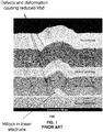
- a hillock that forms on a bottom electrode can cause defects and deformations resulting in a reduction in breakdown voltage of the dielectric film.
- vertical dendrite growth can cause capacitor failure in the field during use.
- the subject disclosure describes, among other things, illustrative embodiments of a thin film capacitor and a method of fabricating a thin film capacitor which has multiple stacked dielectric layers.
- the stacked dielectric layers provide for a change in grain structures in different dielectric layers to reduce or eliminate dendrite formation while maintaining a same or similar composition and grain structure at electrode interfaces to reduce or eliminate charge trapping.
- low temperature deposition of some of the dielectric layers can reduce or eliminate hillock formation on the electrode(s) which could lead to low breakdown voltage.
- the systems and methods described herein provide a composite high-k thin film stack which improves the time-dependent dielectric breakdown of the thin film capacitor.
- Other embodiments are described by the subject disclosure.
- One or more features and/or process steps described in U.S. Patent No. 8,154,850 can be utilized in place of or in addition to one or more features and/or process steps described herein with respect to the exemplary embodiments.
- the disclosure of U.S. Patent No. 8,154,850 is incorporated herein by reference
- One embodiment of the subject disclosure includes a method for fabricating a thin film capacitor.
- the method includes depositing a first dielectric layer on a first electrode layer utilizing a first process that is performed at a first temperature and depositing a second dielectric layer on the first dielectric layer utilizing a second process that forms a randomly-oriented grain structure for the second dielectric layer.
- the method includes depositing a third dielectric layer on the second dielectric layer utilizing a third process that is performed at a second temperature and that forms a columnar-oriented grain structure for the third dielectric layer, where the second temperature is higher than the first temperature.
- the method includes depositing a second electrode layer on the third dielectric layer to form the thin film capacitor.
- One embodiment of the subject disclosure includes a method that includes depositing, via a first process, a first dielectric layer on a first electrode layer at a first temperature, where the first temperature is selected to be below a hillock temperature above which it is determined that hillocks form on the first electrode layer.
- the method can include depositing, via a second process, a second dielectric layer on the first dielectric layer to form a randomly-oriented grain structure for the second dielectric layer.
- the method can include depositing, via a third process, a third dielectric layer on the second dielectric layer to form a columnar-oriented grain structure for the third dielectric layer.
- the method can include depositing a second electrode layer on the third dielectric layer to form the thin film capacitor.
- One embodiment of the subject disclosure includes a thin film capacitor including a substrate, a first electrode layer on the substrate, and a first dielectric layer on the first electrode layer, where the first dielectric layer has a columnar-oriented grain structure.
- the thin film capacitor can include a second dielectric layer on the first dielectric layer, where the second dielectric layer has a randomly-oriented grain structure.
- the thin film capacitor can include a third dielectric layer on the second dielectric layer, where the third dielectric layer has the columnar-oriented grain structure.
- the thin film capacitor can include a second electrode layer on the third dielectric layer, where an average grain size of the first dielectric layer is smaller than an average grain size for the third dielectric layer.
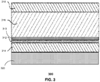
- Capacitor 300 can reduce or eliminate dendrite formation and improve time-dependent dielectric breakdown, while also reducing or eliminating hillock formation along electrodes and reducing or eliminating charge trapping.
- Capacitor 300 can include a first dielectric layer 312, a second dielectric layer 313, and a third dielectric layer 316.
- the dielectric layers 312, 313, 316 can be formed directly on each other.
- the dielectric layers 312, 313, 316 can be formed between electrode layer 314 and electrode layer 318.
- the first dielectric layer 312 can be formed of various materials including Barium Strontium Titanate (BST), Strontium Bismuth Tantalate (SBT), Lead Zirconate Titanate (PZT), Lead Lanthanum Zirconate Titanate (PLZT), any other perovskite or pyrochlore phase ferroelectric film, or a combination thereof.
- the first dielectric layer 312 can be formed by a process and/or formed from material(s) that enable the first dielectric layer to suppress formation of hillocks along the surface of the electrode layer 314.
- the first dielectric layer 312 can be formed by a process and/or formed from material(s) that provide for a particular grain habit in the first dielectric layer, such as vertically-oriented columnar grain structure.
- the second dielectric layer 313 can be formed of various materials including BST, SBT, PZT, PLZT, any other perovskite or pyrochlore phase ferroelectric film, or a combination thereof.
- the second dielectric layer 313 can be formed by a process and/or formed from material(s) that suppress dendrite formation and/or distort the orientation of crystalline columnarity of the first layer while providing an interruption in vertically oriented grain boundaries of the capacitor resulting in an improvement in the time-dependent dielectric breakdown behavior of the capacitor.
- the second dielectric layer 313 can be formed by a process and/or formed from material(s) that provide for a randomly-oriented grain structure in the second dielectric layer.
- the third dielectric layer 316 can be formed of various materials including BST, SBT, PZT, PLZT, any other perovskite or pyrochlore phase ferroelectric film, or a combination thereof.
- the third dielectric layer 316 can be formed by a process and/or formed from material(s) that provide for a columnar vertically-oriented grain structure in the third dielectric layer.
- the third dielectric layer 316 can be formed by a process and/or formed from material(s) that enable achieving desired dielectric properties for the capacitor 300.
- the electrodes 314, 318 can be formed of various materials including platinum, platinum alloy, iridium either solely or in combination with iridium oxide, ruthenium oxide, or Strontium Ruthenium Oxide (SRO), any metal or conductive oxide or any combination of these materials.
- the electrodes 314, 318 can be formed from other conductive materials, including non-metal conductive materials.
- the electrodes 314, 318 can be formed from the same material or can be formed from different materials.
- the capacitor structure with multiple dielectric layers 312, 313, 316 can be formed on a substrate 320.
- the substrate 320 can be formed of various materials including silicon, alumina (including glazed and zirconia toughened alumina (ZTA)), sapphire, silicon-on-sapphire (SOS), silicon carbide, magnesium silicate (including foresterite), any other type of insulating, semi-insulating or semi-conducting material, or any combinations thereof.
- Other layers can also be included in the capacitor 300 such as an insulating layer (e.g., SiO 2 ) and/or a hermetic insulating layer (Si 3 N 4 ).
- the first dielectric layer 312 and the third dielectric layer 316 can have the same or similar crystal grain structure and/or the same or similar dielectric composition.
- Space-charge effects in dielectrics can create a lack of control of the capacitance during product life under bias and losses in high frequency applications.
- Charge trapping can be more pronounced when the dielectric composition and/or the crystal structure habit is different on the interfaces with the upper and lower electrodes of a capacitor.
- the use of the same or similar dielectric composition and/or the same or similar crystal habit (e.g., columnar vertically-oriented grain structure) at the electrode interfaces in capacitor 300 can reduce or eliminate the charge trapping providing identical paths for the charge and discharge portions of the tuning cycle.
- the first, second and third layers 312, 313, 316 can utilize a combination of an undoped BST and a doped BST formulation, or a combination of different ferroelectric materials to facilitate reducing space charge effects and/or improving a temperature dependence of the dielectric properties of the capacitor 300.
- the first and third layers 312, 316 can use one of the doped or undoped BST materials while the second dielectric layer 313 uses the other of the doped or undoped BST materials.
- the thickness of the first dielectric layer 312 and/or the second dielectric layer 313 can be selected so that it is thin enough to not adversely affect the operation of the capacitor 300 but thick enough to enable suppression of hillock formation, suppression of dendrite formation, and/or avoid or reduce charge trapping as described herein.
- the overall thickness of the combination of the first and second dielectric layers 312, 313 can be less than 300A.
- the thickness of the first dielectric layer 312 can be different from the thickness of the second dielectric layer 313.
- the thickness of the first and second dielectric layers 312, 313 can be the same.
- the thickness of the third dielectric layer 316 can be at least two times larger than the thickness of the combination of the first and second dielectric layers 312, 313.
- the thicknesses selected for the first, second and third dielectric layers can be based on various factors including the dielectric material(s) being utilized, the electrode material(s) being utilized, the desired properties of the capacitor, the desired size and/or shape of the capacitor, the operating environment of the capacitor, and so forth.
- a ferroelectric capacitor 400 is illustrated that includes first dielectric layers 312, second dielectric layers 313, and third dielectric layers 316.
- the dielectric layers 312, 313, 316 as described above are formed by a process, formed from material(s) and/or have particular crystal grain structures which provide desired properties to the capacitor 400 including suppression of dendrite formation, suppression of hillock formation and/or improvement of time-dependent dielectric breakdown.
- Capacitor 400 illustrates first and second capacitors 450, 475 that are stacked together sharing a middle electrode 318 and further having a top electrode 418.
- Capacitor 400 can have any number of stacked capacitors that are each formed from the dielectric layers 312, 313, 316. Any number of sets of stacked dielectric layers 312, 313, 316 can be utilized and various other connections would be implemented.
- the sets of dielectric layers that each form capacitors 450, 475 can be the same or similar (e.g., having the same number of layers where corresponding layers in different sets have the same thickness, materials, and/or grain structure).
- the sets of dielectric layers can have the same number of layers but corresponding layers in different sets can have the same or different thickness, materials, and/or grain structure).
- different capacitors stacked together may have different desired properties so that the thicknesses and/or materials forming the corresponding layers in different sets can be different.
- the first and third dielectric layers 312, 316 in each stacked capacitor can have the same grain structure.
- the sets of dielectric layers can have different numbers of layers, such as a bottom capacitor having three dielectric layers (e.g., dielectric layer 316 deposited on dielectric layer 313 deposited on dielectric layer 312), a middle capacitor having five dielectric layers (e.g., dielectric layer 312 deposited on dielectric layer 313 deposited on dielectric layer 316 deposited on dielectric layer 313 deposited on dielectric layer 312), and a top capacitor having three dielectric layers (e.g., dielectric layer 316 deposited on dielectric layer 313 deposited on dielectric layer 312).
- each capacitor of the sets of capacitors can be the same or similar (e.g., using the same processes for each corresponding layer in the different sets).
- the fabrication of each capacitor of the sets of capacitors can be different (e.g., using a different process for a corresponding layer in a different set such as sputtering the first dielectric layer 312 in a bottom capacitor at a first low temperature and sputtering the first dielectric layer 312 in a middle capacitor at a second low temperature).
- the use of different processes to fabricate corresponding layers in different sets of capacitors can be based on various factors including desired properties of the different stacked capacitors (e.g., capacitors 450, 475).
- FIG. 5 depicts an illustrative method 500 for fabricating a multilayer capacitor structure.
- the first electrode layer 314 of conductive material may be deposited or otherwise formed.
- the first electrode layer 314 may be deposited directly onto the substrate 320 or may be deposited onto the substrate that has previously had an insulating layer deposited thereon.
- the first electrode layer 314 can be formed of various materials including platinum, platinum alloy, iridium either solely or in combination with iridium oxide, ruthenium oxide, or SRO, any metal or conductive oxide, or any combination of these materials.
- a first dielectric layer 312 of ferroelectric material can be deposited or otherwise formed on the first electrode layer 314.
- the first dielectric layer 312 can be deposited directly onto the first electrode layer 314.
- the first dielectric layer 312 can be deposited so as to cover an entire top surface of the first electrode layer 314.
- the first dielectric layer 312 can be formed of various materials including BST, SBT, BZN, PZT, PLZT, any other perovskite or pyrochlore phase ferroelectric film, or a combination thereof.
- the first dielectric layer 312 can have a thickness between 50A and 200A, as well as between 200A and 700A. However, other thicknesses can be utilized for the first dielectric layer 312, such as based on the type of dielectric material, the parameters for the capacitor being formed, and so forth. In one embodiment, the thickness of the first dielectric layer 312 can be selected so that it is thin enough to not adversely affect the operation of the capacitor but thick enough to enable suppression of hillock formation and/or avoid or reduce charge trapping as described herein.
- the first dielectric layer 312 can be a layer that suppresses formation of hillocks along the surface of the first electrode layer 314.
- the first dielectric layer 312 can be deposited at a temperature which is low enough to prevent or reduce hillock formation.
- a hillock temperature can be determined for the first electrode layer 314 where the hillock temperature corresponds to the temperature above which hillock formation is likely (e.g., has been observed during testing).
- the deposition temperature for the first dielectric layer 312 can then be chosen to be below the hillock temperature.
- the first dielectric layer 312 can be deposited using a process that enables a columnar-oriented grain structure to be formed, such as via a sputtering process.
- a sputtering process can be performed below the hillock temperature thereby preventing or reducing hillock formation while also reducing grain growth, as compared to a high-temperature sputtering process.
- the first dielectric layer 312 can heal and planarize possible defects and roughness in the first electrode layer 314 when applied directly to the first electrode layer.
- a second dielectric layer 313 of ferroelectric material can be deposited or otherwise formed on the first dielectric layer 312.
- the second dielectric layer 313 can be deposited directly onto the first dielectric layer 312.
- the second dielectric layer 313 can be deposited so as to cover an entire top surface of the first dielectric layer 312.
- the second dielectric layer 313 can be formed of various materials including BST, SBT, BZN, PZT, PLZT, any other perovskite or pyrochlore phase ferroelectric film or a combination thereof.
- the second dielectric layer 313 can have a thickness between 300A and 500A, as well as between 500A and 800A. However, other thicknesses can be utilized for the second dielectric layer 313, such as based on the type of dielectric material, the parameters for the capacitor being formed, and so forth. In one embodiment, the thickness of the second dielectric layer 313 can be selected so that it is thin enough to not adversely affect the operation of the capacitor but thick enough to enable suppression of dendrite formation and/or improvement of the time-dependent dielectric breakdown of the capacitor.
- the second dielectric layer 313 can be a layer that distorts the orientation of crystalline columnarity of the capacitor while providing an interruption in the vertically oriented grain boundaries of the capacitor resulting in an improvement in the time-dependent dielectric breakdown behavior of the capacitor.
- the second dielectric layer 313 can be deposited utilizing a process that forms a randomly-oriented grain structure in the second dielectric layer.
- the second dielectric layer 313 can be deposited utilizing a Metal Organic Deposition (MOD) or Chemical Solution Deposition (CSD) process, such as spin-on deposition or misted deposition.
- the deposition of the second dielectric layer 313 can be performed at a low temperature, such as 400C or lower.
- the second dielectric layer 313 can be deposited using a deposition process with a deposition temperature that is below the hillock temperature thereby preventing or reducing hillock formation while also allowing the random-oriented grain structure in the second dielectric layer.
- thermal processing can be applied after the deposition of the second dielectric layer 313, such as hot plate bakes, oven bakes, rapid thermal processing, vacuum bakes (e.g., in-situ bake while sputtering) and/or high temperature anneals.
- the second dielectric layer 313 can be deposited using other processes that enable a randomly-oriented grain structure to be formed.
- a third dielectric layer 316 of ferroelectric material can be deposited or otherwise formed on the second dielectric layer 313.
- the third dielectric layer 316 can be deposited directly onto the second dielectric layer 313.
- the third dielectric layer 316 can be deposited so as to cover an entire top surface of the second dielectric layer 313.
- the third dielectric layer 316 can be formed of various materials including BST, SBT, PZT, PLZT, any other perovskite or pyrochlore phase ferroelectric film or a combination thereof.
- the third dielectric layer 316 can have a thickness between 300A and 600A, as well as between 600A and 2000A. However, other thicknesses can be utilized for the third dielectric layer 316, such as based on the type of dielectric material, the parameters for the capacitor being formed, and so forth. In one embodiment, the thickness of the third dielectric layer 316 can be selected so that it provides the desired parameters for the capacitor including tunability, conductivity, charge retention, grain size, and so forth.
- the third dielectric layer 316 can be deposited using a process that enables a columnar-oriented grain structure to be formed, such as via a sputtering process such as sputtering with RF, DC or RF/DC power source using a magnetron type cathode for plasma confinement.
- the deposition process can be Chemical Vapor Deposition (CVD) or Pulsed Laser Deposition (PLD) process.
- the sputtering process can be high temperature sputtering, such as 400C or higher. Sputtering can be performed in a reactive environment such as in the presence of oxidizers including O 2 , N 2 O or flourine.
- a second electrode layer 318 of conductive material may be deposited or otherwise formed on the third dielectric layer 316.
- the second electrode layer 318 may be deposited directly onto the third dielectric layer 316.
- the second electrode layer 318 can be formed of various materials including platinum, platinum alloy, iridium either solely or in combination with iridium oxide, ruthenium oxide, or SRO, any metal or conductive oxide, or any combination of these materials.
- the first dielectric layer 312 and the third dielectric layer 316 can have the same or similar crystal grain structure and/or the same or similar dielectric composition.
- Method 500 can overcome or otherwise reduce charge trapping by providing the first dielectric layer 312 and the third dielectric layer 316 with the same or similar crystal grain structure and/or the same or similar dielectric composition.
- the deposition of the first and third dielectric layers 312, 316 can be performed using the same process (e.g., the same sputtering process) or can be performed using different processes (e.g., CVD and PLD) provided that the same or similar crystal structure is achieved for both dielectric layers (e.g., a columnar vertically-oriented grain structure).
- the first, second and third dielectric layers 312, 313, 316 can utilize a combination of an undoped BST and a doped BST formulation, or a combination of different ferroelectric materials to facilitate reducing space charge effects and/or improving a temperature dependence of the dielectric properties of the capacitor.
- the first and third layers 312, 316 can use one of the doped or undoped BST materials while the second dielectric layer 313 uses the other of the doped or undoped BST materials.
- the deposition of the third dielectric layer 316 can be performed at a higher temperature than the deposition of the first dielectric layer 312.
- the first dielectric layer 312 can be sputtered at a first temperature that is below the hillock temperature where hillock formation is likely, while the third dielectric layer 316 is sputtered at a second temperature that promotes grain growth in the third dielectric layer.
- the hillock temperature for the platinum electrode layer can be selected to be 600 C and the first dielectric layer 312 can be sputtered at a first temperature at or below 600 C.
- Other temperatures can be selected so as to reduce or eliminate hillock formation depending on the type of materials being utilized and the deposition processes being employed.
- the grain sizes of the first dielectric layer 312 can be smaller than the grain sizes of the third dielectric layer 316, such as an average grain size of the first dielectric layer being smaller than an average grain size of the third dielectric layer.
- the difference in grain sizes between the first and third dielectric layers 312, 316 can be the result of the different deposition temperatures being utilized.
- the previous steps of dielectric deposition and electrode deposition can be repeated to form any number of stacked capacitors.
- the deposited capacitor layers may be patterned into a mesa structure. Patterning the capacitor layers into a mesa structure can provide access to all electrode layers and capacitor layers for later interconnection.
- a planarizing and/or insulating layer can be deposited on top of the previously deposited layers, such as over the second electrode layer 318 or over third dielectric layer 316.
- the planarizing and/or insulating layer can be etched to form a set of pathways or vias in the capacitor structure. These etched vias can provide conduits for metal interconnection materials to be deposited.
- one or more metal interconnect layers can be deposited.
- the metal interconnect layer(s) can create electrical connections for the thin film capacitor.
- the electrodes can be patterned electrodes and the first, second and third dielectric layers 312, 313 and 316 are formed on the patterned electrodes.
- the electrode layer 314 can only partially cover the substrate 320 due to patterning of the electrode layer on the substrate.
- the dielectric layer electrode layer 314 can still completely cover the patterned electrode layer.
- an additional layer of protective material such as a silicon nitride overcoat, may be deposited on top of the metal interconnect layer and/or gold bumps may be attached to the metal connections to help protect the previously deposited structures.
- FIG. 6 depicts a structure 600 that includes two sets of stacked dielectric layers, which in this example are dielectric layers 312, 313, 316. Any number of sets of stacked dielectric layers 312, 313, 316 can be utilized and various other connections would be implemented.
- the dielectric layer 313 having a random-oriented grain structure is deposited between dielectric layers 312, 316 having columnar-oriented grains structures.
- the deposition process for the dielectric layer 312 and the dielectric layer 316 can be different, such as depositing the dielectric layer 312 at a low temperature which is below the temperature at which hillock formation occurs and depositing the dielectric layer 316 at a high temperature. Similar to the capacitor 400 of FIG. 4 , the stacked capacitors in FIG. 6 share a middle electrode 318.
- one or more insulating layers 660 are deposited on the substrate 320.
- the insulating layer(s) 660 may be formed from SiO 2 and/or Si 3 N 4 .
- the sets of dielectric layers 312, 313, 316 and the electrode layers 314, 318, 418 are patterned to form a mesa structure, to facilitate providing an electrical connection to each electrode layer.
- a planarizing and insulating layer 672 (e.g., an ILD glass layer) can be deposited, patterned and etched to form vias 674.
- a metal interconnect layer 676 can be deposited over the planarizing and insulating layer 672 and into the vias 674 to provide an electrical connection to the electrodes 314, 318, 418.
- a nitride overcoat 678 can be deposited to protect the metal interconnect layer 676 and gold bumps 680 can be deposited to provide electrical contacts for final packaging.
- additional dielectric layers can be added to the layer stack while configuring the stacking such that at the interface with the electrodes the same or similar crystal grain structure and/or the same or similar dielectric composition exists.
- a stack can be formed which is configured as follows: first dielectric layer 313 deposited on second dielectric layer 314 deposited on third dielectric layer 316 deposited on second dielectric layer 314 deposited on first dielectric layer 313.
- the same crystal grain structure (columnar) and the same dielectric composition e.g., BST
- Various deposition processes can be utilized for the dielectric layers in order to achieve a desired grain structure, a desired hillock suppression, a desired dendrite suppression, and/or a desired capacitor properties.
- the deposition techniques can be sputtering, CVD, Atomic Layer Deposition (ALD), Combustion Chemical Vapor Deposition (CCVD), PLD, Physical Vapor Deposition (PVD), and so forth.
- a sputtering target can be selected or fabricated (and utilized in one or more of the exemplary embodiments) according to one or more of the features or process steps of U.S. Patent Publication No. 20140216921 , the disclosure of which is hereby incorporated by reference.
- One or more of the thin film capacitors described with respect to the exemplary embodiments can be utilized in various components including tunable filters, voltage controlled oscillators, tunable phase shifters, tunable matching networks, low-impedance power supplies, decoupling high-frequency signals at an IC bonding pad, mobile phone components (where the mobile phone includes an antenna and a transceiver) or others.
- Integrated circuits including ferroelectric capacitors described with respect to the exemplary embodiments may, for example, be used in portable electronics for low-power wireless communication (e.g., cellular phones, pagers, PDAs, and so forth), directional antenna systems, high clock-rate microphones, miniature DC to DC converters, or other devices.
Landscapes
- Engineering & Computer Science (AREA)
- Power Engineering (AREA)
- Microelectronics & Electronic Packaging (AREA)
- Manufacturing & Machinery (AREA)
- Chemical & Material Sciences (AREA)
- Inorganic Chemistry (AREA)
- Ceramic Engineering (AREA)
- Fixed Capacitors And Capacitor Manufacturing Machines (AREA)
- Semiconductor Integrated Circuits (AREA)
- Ceramic Capacitors (AREA)
Abstract
Description
- This present invention relates, in general, to a thin film dielectric stack, and more particularly, to systems of and methods for manufacturing a thin film multilayer tunable dielectric stack.
- Ferroelectric capacitors have various uses in RF systems including as voltage-tunable devices. Some benefits of ferroelectric capacitors are small size, integration of different values and functions of capacitance, and low cost. Applications for ferroelectric capacitors may include tunable filters, voltage controlled oscillators, tunable phase shifters, tunable matching networks, low-impedance power supplies, decoupling high-frequency signals at an IC bonding pad, or others. Integrated circuits including ferroelectric capacitors may, for example, be used in portable electronics for low-power wireless communication (e.g., cellular phones, pagers, PDAs, and so forth), directional antenna systems, high clock-rate microphones, miniature DC to DC converters, or other devices.
- The fabrication of tunable ferroelectric capacitors can sometimes lead to undesired conditions. For example as shown in
FIG. 1 , a hillock that forms on a bottom electrode can cause defects and deformations resulting in a reduction in breakdown voltage of the dielectric film. As another example shown inFIG. 2 , vertical dendrite growth can cause capacitor failure in the field during use. - Reference will now be made to the accompanying drawings, which are not necessarily drawn to scale, and wherein:
-
Figure 1 illustrates an image of a prior art ferroelectric capacitor having hillock formation. -
Figure 2 illustrates an image of a prior art ferroelectric capacitor having dendrite formation. -
Figure 3 illustrates an exemplary embodiment of a thin film capacitor having multiple dielectric layers. -
Figure 4 illustrates another exemplary embodiment of a thin film capacitor having multiple dielectric layers. -
Figure 5 illustrates an exemplary embodiment of a method of fabricating a thin film capacitor to reduce or eliminate hillock formation and/or dendrite formation and/or to improve time-dependent dielectric breakdown. -
Figure 6 illustrates another exemplary embodiment of a thin film capacitor having multiple dielectric layers. - The subject disclosure describes, among other things, illustrative embodiments of a thin film capacitor and a method of fabricating a thin film capacitor which has multiple stacked dielectric layers. The stacked dielectric layers provide for a change in grain structures in different dielectric layers to reduce or eliminate dendrite formation while maintaining a same or similar composition and grain structure at electrode interfaces to reduce or eliminate charge trapping. In one or more embodiments, low temperature deposition of some of the dielectric layers can reduce or eliminate hillock formation on the electrode(s) which could lead to low breakdown voltage. The systems and methods described herein provide a composite high-k thin film stack which improves the time-dependent dielectric breakdown of the thin film capacitor. Other embodiments are described by the subject disclosure. One or more features and/or process steps described in
U.S. Patent No. 8,154,850 can be utilized in place of or in addition to one or more features and/or process steps described herein with respect to the exemplary embodiments. The disclosure ofU.S. Patent No. 8,154,850 is incorporated herein by reference in its entirety. - One embodiment of the subject disclosure includes a method for fabricating a thin film capacitor. The method includes depositing a first dielectric layer on a first electrode layer utilizing a first process that is performed at a first temperature and depositing a second dielectric layer on the first dielectric layer utilizing a second process that forms a randomly-oriented grain structure for the second dielectric layer. The method includes depositing a third dielectric layer on the second dielectric layer utilizing a third process that is performed at a second temperature and that forms a columnar-oriented grain structure for the third dielectric layer, where the second temperature is higher than the first temperature. The method includes depositing a second electrode layer on the third dielectric layer to form the thin film capacitor.
- One embodiment of the subject disclosure includes a method that includes depositing, via a first process, a first dielectric layer on a first electrode layer at a first temperature, where the first temperature is selected to be below a hillock temperature above which it is determined that hillocks form on the first electrode layer. The method can include depositing, via a second process, a second dielectric layer on the first dielectric layer to form a randomly-oriented grain structure for the second dielectric layer. The method can include depositing, via a third process, a third dielectric layer on the second dielectric layer to form a columnar-oriented grain structure for the third dielectric layer. The method can include depositing a second electrode layer on the third dielectric layer to form the thin film capacitor.
- One embodiment of the subject disclosure includes a thin film capacitor including a substrate, a first electrode layer on the substrate, and a first dielectric layer on the first electrode layer, where the first dielectric layer has a columnar-oriented grain structure. The thin film capacitor can include a second dielectric layer on the first dielectric layer, where the second dielectric layer has a randomly-oriented grain structure. The thin film capacitor can include a third dielectric layer on the second dielectric layer, where the third dielectric layer has the columnar-oriented grain structure. The thin film capacitor can include a second electrode layer on the third dielectric layer, where an average grain size of the first dielectric layer is smaller than an average grain size for the third dielectric layer.
- Referring to
FIG. 3 , aferroelectric capacitor 300 is illustrated that can reduce or eliminate dendrite formation and improve time-dependent dielectric breakdown, while also reducing or eliminating hillock formation along electrodes and reducing or eliminating charge trapping.Capacitor 300 can include a firstdielectric layer 312, a seconddielectric layer 313, and a thirddielectric layer 316. Thedielectric layers dielectric layers electrode layer 314 andelectrode layer 318. - The first
dielectric layer 312 can be formed of various materials including Barium Strontium Titanate (BST), Strontium Bismuth Tantalate (SBT), Lead Zirconate Titanate (PZT), Lead Lanthanum Zirconate Titanate (PLZT), any other perovskite or pyrochlore phase ferroelectric film, or a combination thereof. The firstdielectric layer 312 can be formed by a process and/or formed from material(s) that enable the first dielectric layer to suppress formation of hillocks along the surface of theelectrode layer 314. The firstdielectric layer 312 can be formed by a process and/or formed from material(s) that provide for a particular grain habit in the first dielectric layer, such as vertically-oriented columnar grain structure. - The second
dielectric layer 313 can be formed of various materials including BST, SBT, PZT, PLZT, any other perovskite or pyrochlore phase ferroelectric film, or a combination thereof. The seconddielectric layer 313 can be formed by a process and/or formed from material(s) that suppress dendrite formation and/or distort the orientation of crystalline columnarity of the first layer while providing an interruption in vertically oriented grain boundaries of the capacitor resulting in an improvement in the time-dependent dielectric breakdown behavior of the capacitor. In one embodiment, the seconddielectric layer 313 can be formed by a process and/or formed from material(s) that provide for a randomly-oriented grain structure in the second dielectric layer. - The third
dielectric layer 316 can be formed of various materials including BST, SBT, PZT, PLZT, any other perovskite or pyrochlore phase ferroelectric film, or a combination thereof. The thirddielectric layer 316 can be formed by a process and/or formed from material(s) that provide for a columnar vertically-oriented grain structure in the third dielectric layer. The thirddielectric layer 316 can be formed by a process and/or formed from material(s) that enable achieving desired dielectric properties for thecapacitor 300. - The
electrodes electrodes electrodes - The capacitor structure with multiple
dielectric layers substrate 320. Thesubstrate 320 can be formed of various materials including silicon, alumina (including glazed and zirconia toughened alumina (ZTA)), sapphire, silicon-on-sapphire (SOS), silicon carbide, magnesium silicate (including foresterite), any other type of insulating, semi-insulating or semi-conducting material, or any combinations thereof. Other layers can also be included in thecapacitor 300 such as an insulating layer (e.g., SiO2) and/or a hermetic insulating layer (Si3N4). - In one embodiment, the first
dielectric layer 312 and the thirddielectric layer 316 can have the same or similar crystal grain structure and/or the same or similar dielectric composition. Space-charge effects in dielectrics can create a lack of control of the capacitance during product life under bias and losses in high frequency applications. Charge trapping can be more pronounced when the dielectric composition and/or the crystal structure habit is different on the interfaces with the upper and lower electrodes of a capacitor. The use of the same or similar dielectric composition and/or the same or similar crystal habit (e.g., columnar vertically-oriented grain structure) at the electrode interfaces incapacitor 300 can reduce or eliminate the charge trapping providing identical paths for the charge and discharge portions of the tuning cycle. - In one embodiment, the first, second and
third layers capacitor 300. For instance, the first andthird layers dielectric layer 313 uses the other of the doped or undoped BST materials. - In one embodiment, the thickness of the first
dielectric layer 312 and/or the seconddielectric layer 313 can be selected so that it is thin enough to not adversely affect the operation of thecapacitor 300 but thick enough to enable suppression of hillock formation, suppression of dendrite formation, and/or avoid or reduce charge trapping as described herein. As an example, the overall thickness of the combination of the first and seconddielectric layers first dielectric layer 312 can be different from the thickness of thesecond dielectric layer 313. In another embodiment, the thickness of the first and seconddielectric layers dielectric layer 316 can be at least two times larger than the thickness of the combination of the first and seconddielectric layers - Referring to
FIG. 4 , a ferroelectric capacitor 400 is illustrated that includes firstdielectric layers 312, seconddielectric layers 313, and third dielectric layers 316. Thedielectric layers second capacitors middle electrode 318 and further having atop electrode 418. - Capacitor 400 can have any number of stacked capacitors that are each formed from the
dielectric layers dielectric layers form capacitors dielectric layers dielectric layer 316 deposited ondielectric layer 313 deposited on dielectric layer 312), a middle capacitor having five dielectric layers (e.g.,dielectric layer 312 deposited ondielectric layer 313 deposited ondielectric layer 316 deposited ondielectric layer 313 deposited on dielectric layer 312), and a top capacitor having three dielectric layers (e.g.,dielectric layer 316 deposited ondielectric layer 313 deposited on dielectric layer 312). - In one embodiment, the fabrication of each capacitor of the sets of capacitors (e.g.,
capacitors 450, 475) can be the same or similar (e.g., using the same processes for each corresponding layer in the different sets). In another embodiment, the fabrication of each capacitor of the sets of capacitors can be different (e.g., using a different process for a corresponding layer in a different set such as sputtering thefirst dielectric layer 312 in a bottom capacitor at a first low temperature and sputtering thefirst dielectric layer 312 in a middle capacitor at a second low temperature). The use of different processes to fabricate corresponding layers in different sets of capacitors can be based on various factors including desired properties of the different stacked capacitors (e.g.,capacitors 450, 475). -
FIG. 5 depicts anillustrative method 500 for fabricating a multilayer capacitor structure. At 502, thefirst electrode layer 314 of conductive material may be deposited or otherwise formed. For example, thefirst electrode layer 314 may be deposited directly onto thesubstrate 320 or may be deposited onto the substrate that has previously had an insulating layer deposited thereon. Thefirst electrode layer 314 can be formed of various materials including platinum, platinum alloy, iridium either solely or in combination with iridium oxide, ruthenium oxide, or SRO, any metal or conductive oxide, or any combination of these materials. - At 504, a first
dielectric layer 312 of ferroelectric material can be deposited or otherwise formed on thefirst electrode layer 314. In one embodiment, thefirst dielectric layer 312 can be deposited directly onto thefirst electrode layer 314. In another embodiment, thefirst dielectric layer 312 can be deposited so as to cover an entire top surface of thefirst electrode layer 314. Thefirst dielectric layer 312 can be formed of various materials including BST, SBT, BZN, PZT, PLZT, any other perovskite or pyrochlore phase ferroelectric film, or a combination thereof. - The
first dielectric layer 312 can have a thickness between 50A and 200A, as well as between 200A and 700A. However, other thicknesses can be utilized for thefirst dielectric layer 312, such as based on the type of dielectric material, the parameters for the capacitor being formed, and so forth. In one embodiment, the thickness of thefirst dielectric layer 312 can be selected so that it is thin enough to not adversely affect the operation of the capacitor but thick enough to enable suppression of hillock formation and/or avoid or reduce charge trapping as described herein. - The
first dielectric layer 312 can be a layer that suppresses formation of hillocks along the surface of thefirst electrode layer 314. As an example, thefirst dielectric layer 312 can be deposited at a temperature which is low enough to prevent or reduce hillock formation. In one embodiment, a hillock temperature can be determined for thefirst electrode layer 314 where the hillock temperature corresponds to the temperature above which hillock formation is likely (e.g., has been observed during testing). In this embodiment, the deposition temperature for thefirst dielectric layer 312 can then be chosen to be below the hillock temperature. - In one embodiment, the
first dielectric layer 312 can be deposited using a process that enables a columnar-oriented grain structure to be formed, such as via a sputtering process. In another embodiment for depositing thefirst dielectric layer 312, a sputtering process can be performed below the hillock temperature thereby preventing or reducing hillock formation while also reducing grain growth, as compared to a high-temperature sputtering process. In one embodiment, thefirst dielectric layer 312 can heal and planarize possible defects and roughness in thefirst electrode layer 314 when applied directly to the first electrode layer. - At 506, a
second dielectric layer 313 of ferroelectric material can be deposited or otherwise formed on thefirst dielectric layer 312. In one embodiment, thesecond dielectric layer 313 can be deposited directly onto thefirst dielectric layer 312. In another embodiment, thesecond dielectric layer 313 can be deposited so as to cover an entire top surface of thefirst dielectric layer 312. Thesecond dielectric layer 313 can be formed of various materials including BST, SBT, BZN, PZT, PLZT, any other perovskite or pyrochlore phase ferroelectric film or a combination thereof. - The
second dielectric layer 313 can have a thickness between 300A and 500A, as well as between 500A and 800A. However, other thicknesses can be utilized for thesecond dielectric layer 313, such as based on the type of dielectric material, the parameters for the capacitor being formed, and so forth. In one embodiment, the thickness of thesecond dielectric layer 313 can be selected so that it is thin enough to not adversely affect the operation of the capacitor but thick enough to enable suppression of dendrite formation and/or improvement of the time-dependent dielectric breakdown of the capacitor. - The
second dielectric layer 313 can be a layer that distorts the orientation of crystalline columnarity of the capacitor while providing an interruption in the vertically oriented grain boundaries of the capacitor resulting in an improvement in the time-dependent dielectric breakdown behavior of the capacitor. As an example, thesecond dielectric layer 313 can be deposited utilizing a process that forms a randomly-oriented grain structure in the second dielectric layer. For instance, thesecond dielectric layer 313 can be deposited utilizing a Metal Organic Deposition (MOD) or Chemical Solution Deposition (CSD) process, such as spin-on deposition or misted deposition. In one embodiment, the deposition of thesecond dielectric layer 313 can be performed at a low temperature, such as 400C or lower. In another embodiment, thesecond dielectric layer 313 can be deposited using a deposition process with a deposition temperature that is below the hillock temperature thereby preventing or reducing hillock formation while also allowing the random-oriented grain structure in the second dielectric layer. - In one embodiment, thermal processing can be applied after the deposition of the
second dielectric layer 313, such as hot plate bakes, oven bakes, rapid thermal processing, vacuum bakes (e.g., in-situ bake while sputtering) and/or high temperature anneals. In one embodiment, thesecond dielectric layer 313 can be deposited using other processes that enable a randomly-oriented grain structure to be formed. - At 508, a third
dielectric layer 316 of ferroelectric material can be deposited or otherwise formed on thesecond dielectric layer 313. In one embodiment, the thirddielectric layer 316 can be deposited directly onto thesecond dielectric layer 313. In another embodiment, the thirddielectric layer 316 can be deposited so as to cover an entire top surface of thesecond dielectric layer 313. The thirddielectric layer 316 can be formed of various materials including BST, SBT, PZT, PLZT, any other perovskite or pyrochlore phase ferroelectric film or a combination thereof. - The third
dielectric layer 316 can have a thickness between 300A and 600A, as well as between 600A and 2000A. However, other thicknesses can be utilized for the thirddielectric layer 316, such as based on the type of dielectric material, the parameters for the capacitor being formed, and so forth. In one embodiment, the thickness of the thirddielectric layer 316 can be selected so that it provides the desired parameters for the capacitor including tunability, conductivity, charge retention, grain size, and so forth. - In one embodiment, the third
dielectric layer 316 can be deposited using a process that enables a columnar-oriented grain structure to be formed, such as via a sputtering process such as sputtering with RF, DC or RF/DC power source using a magnetron type cathode for plasma confinement. The deposition process can be Chemical Vapor Deposition (CVD) or Pulsed Laser Deposition (PLD) process. The sputtering process can be high temperature sputtering, such as 400C or higher. Sputtering can be performed in a reactive environment such as in the presence of oxidizers including O2, N2O or flourine. - At 510, a
second electrode layer 318 of conductive material may be deposited or otherwise formed on the thirddielectric layer 316. For example, thesecond electrode layer 318 may be deposited directly onto the thirddielectric layer 316. Thesecond electrode layer 318 can be formed of various materials including platinum, platinum alloy, iridium either solely or in combination with iridium oxide, ruthenium oxide, or SRO, any metal or conductive oxide, or any combination of these materials. - In one embodiment, the
first dielectric layer 312 and the thirddielectric layer 316 can have the same or similar crystal grain structure and/or the same or similar dielectric composition.Method 500 can overcome or otherwise reduce charge trapping by providing thefirst dielectric layer 312 and the thirddielectric layer 316 with the same or similar crystal grain structure and/or the same or similar dielectric composition. In one embodiment, the deposition of the first and thirddielectric layers - In one embodiment, the first, second and third
dielectric layers third layers second dielectric layer 313 uses the other of the doped or undoped BST materials. - In one embodiment, the deposition of the third
dielectric layer 316 can be performed at a higher temperature than the deposition of thefirst dielectric layer 312. For instance, thefirst dielectric layer 312 can be sputtered at a first temperature that is below the hillock temperature where hillock formation is likely, while the thirddielectric layer 316 is sputtered at a second temperature that promotes grain growth in the third dielectric layer. As an example, where thefirst electrode layer 314 is platinum, the hillock temperature for the platinum electrode layer can be selected to be 600 C and thefirst dielectric layer 312 can be sputtered at a first temperature at or below 600 C. Other temperatures can be selected so as to reduce or eliminate hillock formation depending on the type of materials being utilized and the deposition processes being employed. - In one embodiment, the grain sizes of the
first dielectric layer 312 can be smaller than the grain sizes of the thirddielectric layer 316, such as an average grain size of the first dielectric layer being smaller than an average grain size of the third dielectric layer. As an example, the difference in grain sizes between the first and thirddielectric layers - At 512, the previous steps of dielectric deposition and electrode deposition can be repeated to form any number of stacked capacitors.
- In one embodiment, the deposited capacitor layers may be patterned into a mesa structure. Patterning the capacitor layers into a mesa structure can provide access to all electrode layers and capacitor layers for later interconnection.
- In one embodiment, a planarizing and/or insulating layer can be deposited on top of the previously deposited layers, such as over the
second electrode layer 318 or over thirddielectric layer 316. The planarizing and/or insulating layer can be etched to form a set of pathways or vias in the capacitor structure. These etched vias can provide conduits for metal interconnection materials to be deposited. - In one embodiment, such as following deposition and etching of the planarizing and/or insulating layer if such layer(s) are deposited, one or more metal interconnect layers can be deposited. The metal interconnect layer(s) can create electrical connections for the thin film capacitor.
- In one embodiment, the electrodes can be patterned electrodes and the first, second and third
dielectric layers electrode layer 314 can only partially cover thesubstrate 320 due to patterning of the electrode layer on the substrate. In one embodiment, the dielectriclayer electrode layer 314 can still completely cover the patterned electrode layer. - In one embodiment following deposition of the metal interconnect layer, an additional layer of protective material, such as a silicon nitride overcoat, may be deposited on top of the metal interconnect layer and/or gold bumps may be attached to the metal connections to help protect the previously deposited structures.
-
FIG. 6 depicts astructure 600 that includes two sets of stacked dielectric layers, which in this example aredielectric layers dielectric layers dielectric layer 313 having a random-oriented grain structure is deposited betweendielectric layers dielectric layer 312 and thedielectric layer 316 can be different, such as depositing thedielectric layer 312 at a low temperature which is below the temperature at which hillock formation occurs and depositing thedielectric layer 316 at a high temperature. Similar to the capacitor 400 ofFIG. 4 , the stacked capacitors inFIG. 6 share amiddle electrode 318. - In one embodiment, one or more
insulating layers 660 are deposited on thesubstrate 320. The insulating layer(s) 660 may be formed from SiO2 and/or Si3N4. The sets ofdielectric layers - In one embodiment, a planarizing and insulating layer 672 (e.g., an ILD glass layer) can be deposited, patterned and etched to form
vias 674. Ametal interconnect layer 676 can be deposited over the planarizing and insulatinglayer 672 and into thevias 674 to provide an electrical connection to theelectrodes nitride overcoat 678 can be deposited to protect themetal interconnect layer 676 andgold bumps 680 can be deposited to provide electrical contacts for final packaging. - Upon reviewing the aforementioned embodiments, it would be evident to an artisan with ordinary skill in the art that said embodiments can be modified, reduced, or enhanced without departing from the scope of the claims described below. For example, additional dielectric layers can be added to the layer stack while configuring the stacking such that at the interface with the electrodes the same or similar crystal grain structure and/or the same or similar dielectric composition exists. For instance, a stack can be formed which is configured as follows: first
dielectric layer 313 deposited on seconddielectric layer 314 deposited on thirddielectric layer 316 deposited on seconddielectric layer 314 deposited on firstdielectric layer 313. In this example, the same crystal grain structure (columnar) and the same dielectric composition (e.g., BST) exists at the electrode interfaces since it is the same firstdielectric layer 313 making contact with the opposing electrodes. - Various deposition processes can be utilized for the dielectric layers in order to achieve a desired grain structure, a desired hillock suppression, a desired dendrite suppression, and/or a desired capacitor properties. For example, the deposition techniques can be sputtering, CVD, Atomic Layer Deposition (ALD), Combustion Chemical Vapor Deposition (CCVD), PLD, Physical Vapor Deposition (PVD), and so forth. In one embodiment, a sputtering target can be selected or fabricated (and utilized in one or more of the exemplary embodiments) according to one or more of the features or process steps of
U.S. Patent Publication No. 20140216921 , the disclosure of which is hereby incorporated by reference. - One or more of the thin film capacitors described with respect to the exemplary embodiments can be utilized in various components including tunable filters, voltage controlled oscillators, tunable phase shifters, tunable matching networks, low-impedance power supplies, decoupling high-frequency signals at an IC bonding pad, mobile phone components (where the mobile phone includes an antenna and a transceiver) or others. Integrated circuits including ferroelectric capacitors described with respect to the exemplary embodiments may, for example, be used in portable electronics for low-power wireless communication (e.g., cellular phones, pagers, PDAs, and so forth), directional antenna systems, high clock-rate microphones, miniature DC to DC converters, or other devices.
- Other embodiments can be applied to the subject disclosure without departing from the scope of the claims described below.
- The illustrations of embodiments described herein are intended to provide a general understanding of the structure of various embodiments, and they are not intended to serve as a complete description of all the elements and features of apparatus and systems that might make use of the structures described herein. Many other embodiments will be apparent to those of skill in the art upon reviewing the above description. Other embodiments may be utilized and derived therefrom, such that structural and logical substitutions and changes may be made without departing from the scope of this disclosure. Figures are also merely representational and may not be drawn to scale. Certain proportions thereof may be exaggerated, while others may be minimized. Accordingly, the specification and drawings are to be regarded in an illustrative rather than a restrictive sense.
- Although specific embodiments have been illustrated and described herein, it should be appreciated that any arrangement calculated to achieve the same purpose may be substituted for the specific embodiments shown. This disclosure is intended to cover any and all adaptations or variations of various embodiments. Combinations of the above embodiments, and other embodiments not specifically described herein, are contemplated by the subject disclosure.
- The Abstract of the Disclosure is provided with the understanding that it will not be used to interpret or limit the scope or meaning of the claims. In addition, in the foregoing Detailed Description, it can be seen that various features are grouped together in a single embodiment for the purpose of streamlining the disclosure. This method of disclosure is not to be interpreted as reflecting an intention that the claimed embodiments require more features than are expressly recited in each claim. Rather, as the following claims reflect, inventive subject matter lies in less than all features of a single disclosed embodiment. Thus the following claims are hereby incorporated into the Detailed Description, with each claim standing on its own as a separately claimed subject matter.
Claims (15)
- A method for fabricating a thin film capacitor, the method comprising:depositing a first dielectric layer on a first electrode layer utilizing a first process that is performed at a first temperature;depositing a second dielectric layer on the first dielectric layer utilizing a second process that forms a randomly-oriented grain structure for the second dielectric layer;depositing a third dielectric layer on the second dielectric layer utilizing a third process that is performed at a second temperature and that forms a columnar-oriented grain structure for the third dielectric layer, wherein the second temperature is higher than the first temperature; anddepositing a second electrode layer on the third dielectric layer to form the thin film capacitor.
- The method of claim 1, wherein the first process forms a columnar-oriented grain structure for the first dielectric layer.
- The method of claim 1, wherein the first and third dielectric layers are formed from the same material.
- The method of claim 1, wherein an average grain size of the first dielectric layer is smaller than an average grain size for the third dielectric layer.
- The method of claim 1, wherein the second temperature is greater than 400 C, and further comprising:determining the first temperature according to a material of the first electrode layer and according to a determination of a hillock temperature above which hillocks form on the material, wherein the first temperature is below the hillock temperature.
- The method of claim 1, wherein the first and third processes are sputtering processes.
- The method of claim 1, wherein the second process is one of a metal organic deposition process or a chemical solution deposition process.
- The method of claim 1, wherein the first electrode layer is a patterned electrode that only partially covers a substrate.
- The method of claim 1, further comprising repeating the depositing of the first, second and third dielectric layers and repeating the depositing of the second electrode to form multi-stacked capacitors.
- The method of claim 1, further comprising:depositing the first electrode layer on a substrate; anddepositing a metal interconnect layer to provide electrical connections for the thin film capacitor.
- The method of claim 1, wherein the first, second and third dielectric layers comprise barium strontium titanate.
- The method of claim 1, further comprising:depositing a planarizing and insulating layer following patterning of the first, second and third layers; andetching the planarizing and insulating layer to form vias.
- The method of claim 1, wherein the first temperature is selected to be below a hillock temperature above which it is determined that hillocks form on the first electrode layer.
- A thin film capacitor comprising:a substrate;a first electrode layer on the substrate;a first dielectric layer on the first electrode layer, wherein the first dielectric layer has a columnar-oriented grain structure;a second dielectric layer on the first dielectric layer, wherein the second dielectric layer has a randomly-oriented grain structure;a third dielectric layer on the second dielectric layer, wherein the third dielectric layer has the columnar-oriented grain structure; anda second electrode layer on the third dielectric layer, wherein an average grain size of the first dielectric layer is smaller than an average grain size for the third dielectric layer.
- The thin film capacitor of claim 14, further comprising:a fourth dielectric layer on the second electrode layer, wherein the fourth dielectric layer has a columnar-oriented grain structure;a fifth dielectric layer on the fourth dielectric layer, wherein the fifth dielectric layer has a randomly-oriented grain structure;a sixth dielectric layer on the fifth dielectric layer, wherein the sixth dielectric layer has the columnar-oriented grain structure; anda third electrode layer on the sixth dielectric layer,wherein the first, second, third, fourth, fifth and sixth dielectric layers comprise barium strontium titanate.
Applications Claiming Priority (1)
| Application Number | Priority Date | Filing Date | Title |
|---|---|---|---|
| US14/642,222 US10115527B2 (en) | 2015-03-09 | 2015-03-09 | Thin film dielectric stack |
Publications (1)
| Publication Number | Publication Date |
|---|---|
| EP3067947A1 true EP3067947A1 (en) | 2016-09-14 |
Family
ID=55521590
Family Applications (1)
| Application Number | Title | Priority Date | Filing Date |
|---|---|---|---|
| EP16159278.7A Withdrawn EP3067947A1 (en) | 2015-03-09 | 2016-03-08 | A thin film dielectric stack |
Country Status (4)
| Country | Link |
|---|---|
| US (1) | US10115527B2 (en) |
| EP (1) | EP3067947A1 (en) |
| CN (1) | CN105957714B (en) |
| CA (1) | CA2922956C (en) |
Cited By (2)
| Publication number | Priority date | Publication date | Assignee | Title |
|---|---|---|---|---|
| US10115527B2 (en) | 2015-03-09 | 2018-10-30 | Blackberry Limited | Thin film dielectric stack |
| CN120955006A (en) * | 2025-08-11 | 2025-11-14 | 浙江化讯半导体材料有限公司 | A method for temporary bonding and debonding of semiconductor devices |
Families Citing this family (15)
| Publication number | Priority date | Publication date | Assignee | Title |
|---|---|---|---|---|
| US10418181B2 (en) * | 2016-04-20 | 2019-09-17 | Eulex Components Inc | Single layer capacitors |
| US10297658B2 (en) | 2016-06-16 | 2019-05-21 | Blackberry Limited | Method and apparatus for a thin film dielectric stack |
| KR102712633B1 (en) * | 2016-11-18 | 2024-10-02 | 삼성전기주식회사 | Thin film capacitor |
| KR102712632B1 (en) * | 2016-11-23 | 2024-10-02 | 삼성전기주식회사 | Thin-film ceramic capacitor |
| US10896950B2 (en) * | 2017-02-27 | 2021-01-19 | Nxp Usa, Inc. | Method and apparatus for a thin film dielectric stack |
| US10332687B2 (en) | 2017-10-23 | 2019-06-25 | Blackberry Limited | Tunable coplanar capacitor with vertical tuning and lateral RF path and methods for manufacturing thereof |
| US10497774B2 (en) | 2017-10-23 | 2019-12-03 | Blackberry Limited | Small-gap coplanar tunable capacitors and methods for manufacturing thereof |
| US11049887B2 (en) * | 2017-11-10 | 2021-06-29 | Applied Materials, Inc. | Layer stack for display applications |
| US10923286B2 (en) | 2018-02-21 | 2021-02-16 | Nxp Usa, Inc. | Method and apparatus for compensating for high thermal expansion coefficient mismatch of a stacked device |
| US11673161B2 (en) | 2019-03-11 | 2023-06-13 | Technetics Group Llc | Methods of manufacturing electrostatic chucks |
| WO2020264519A1 (en) | 2019-06-27 | 2020-12-30 | Eulex Components Inc | Ceramic microelectronic devices and methods of their manufacture |
| WO2021053682A1 (en) * | 2019-09-22 | 2021-03-25 | Technion Research & Development Foundation Limited | Superconductor composites and devices comprising same |
| CN113594365B (en) * | 2020-04-30 | 2024-08-20 | 中芯国际集成电路制造(上海)有限公司 | Semiconductor structure and method for forming the same |
| KR102926515B1 (en) * | 2020-10-29 | 2026-02-10 | 삼성전자주식회사 | Capacitor, semiconductor device inclduing the same |
| US11862607B2 (en) * | 2021-08-16 | 2024-01-02 | Micron Technology, Inc. | Composite dielectric structures for semiconductor die assemblies and associated systems and methods |
Citations (4)
| Publication number | Priority date | Publication date | Assignee | Title |
|---|---|---|---|---|
| EP0681327A2 (en) * | 1994-04-28 | 1995-11-08 | Xerox Corporation | Dual dielectric capping layers for hillock suppression in metal layers in thin film structures |
| JP2007088437A (en) * | 2005-08-24 | 2007-04-05 | Tokyo Electron Ltd | Dielectric film having ABOx type perovskite crystal structure and method for forming dielectric film having ABOx type perovskite crystal structure |
| US20080278887A1 (en) * | 2007-05-11 | 2008-11-13 | Marina Zelner | Systems and Methods for a Thin Film Capacitor Having a Composite High-K Thin Film Stack |
| US20140216921A1 (en) | 2013-02-04 | 2014-08-07 | Research In Motion Rf, Inc. | Method of forming a target for deposition of doped dielectric films by sputtering |
Family Cites Families (24)
| Publication number | Priority date | Publication date | Assignee | Title |
|---|---|---|---|---|
| JP3476932B2 (en) | 1994-12-06 | 2003-12-10 | シャープ株式会社 | Ferroelectric thin film, substrate coated with ferroelectric thin film, and method of manufacturing ferroelectric thin film |
| JP3480624B2 (en) | 1995-06-09 | 2003-12-22 | シャープ株式会社 | Ferroelectric thin film coated substrate, method of manufacturing the same, and capacitor structure element |
| KR100199095B1 (en) | 1995-12-27 | 1999-06-15 | 구본준 | Capacitor Structure of Semiconductor Memory Cell and Manufacturing Method Thereof |
| US5745335A (en) | 1996-06-27 | 1998-04-28 | Gennum Corporation | Multi-layer film capacitor structures and method |
| AU1539900A (en) | 1998-11-30 | 2000-06-19 | Interuniversitair Micro-Elektronica Centrum | Method of fabrication of a ferro-electric capacitor and method of growing a pzt layer on a substrate |
| DE19856457A1 (en) * | 1998-12-03 | 2000-06-08 | Abb Research Ltd | Film for a film capacitor and film capacitor |
| KR20020092945A (en) | 2000-02-03 | 2002-12-12 | 케이스 웨스턴 리저브 유니버시티 | High power capacitors from thin layers of metal powder or metal sponge particles |
| US6407929B1 (en) | 2000-06-29 | 2002-06-18 | Intel Corporation | Electronic package having embedded capacitors and method of fabrication therefor |
| JP2002075783A (en) * | 2000-08-25 | 2002-03-15 | Alps Electric Co Ltd | Thin film capacitor for temperature compensation |
| US6500754B1 (en) | 2000-11-02 | 2002-12-31 | Advanced Micro Devices, Inc. | Anneal hillock suppression method in integrated circuit interconnects |
| US6566147B2 (en) | 2001-02-02 | 2003-05-20 | Micron Technology, Inc. | Method for controlling deposition of dielectric films |
| JP2004152796A (en) | 2002-10-28 | 2004-05-27 | Toshiba Corp | Semiconductor device and manufacturing method thereof |
| US6909589B2 (en) | 2002-11-20 | 2005-06-21 | Corporation For National Research Initiatives | MEMS-based variable capacitor |
| US20040175585A1 (en) | 2003-03-05 | 2004-09-09 | Qin Zou | Barium strontium titanate containing multilayer structures on metal foils |
| US7312091B2 (en) | 2003-07-25 | 2007-12-25 | Samsung Electronics Co., Ltd. | Methods for forming a ferroelectric layer and capacitor and FRAM using the same |
| US7224040B2 (en) | 2003-11-28 | 2007-05-29 | Gennum Corporation | Multi-level thin film capacitor on a ceramic substrate |
| KR100725451B1 (en) | 2005-06-07 | 2007-06-07 | 삼성전자주식회사 | Manufacturing method of ferroelectric capacitor and manufacturing method of semiconductor device using same |
| US8467169B2 (en) | 2007-03-22 | 2013-06-18 | Research In Motion Rf, Inc. | Capacitors adapted for acoustic resonance cancellation |
| US8194387B2 (en) | 2009-03-20 | 2012-06-05 | Paratek Microwave, Inc. | Electrostrictive resonance suppression for tunable capacitors |
| FR2981346B1 (en) | 2011-10-18 | 2014-01-24 | Saint Gobain | PROCESS FOR THERMALLY TREATING SILVER LAYERS |
| US9178008B2 (en) | 2012-08-10 | 2015-11-03 | Taiwan Semiconductor Manufacturing Company, Ltd. | Metal-insulator-metal capacitor with current leakage protection |
| US9331262B2 (en) | 2013-05-20 | 2016-05-03 | Tdk Corporation | Thin film piezoelectric element, thin film piezoelectric actuator, thin film piezoelectric sensor, hard drive disk, and inkjet printer device |
| US10115527B2 (en) | 2015-03-09 | 2018-10-30 | Blackberry Limited | Thin film dielectric stack |
| US10297658B2 (en) | 2016-06-16 | 2019-05-21 | Blackberry Limited | Method and apparatus for a thin film dielectric stack |
-
2015
- 2015-03-09 US US14/642,222 patent/US10115527B2/en active Active
-
2016
- 2016-03-04 CA CA2922956A patent/CA2922956C/en active Active
- 2016-03-08 EP EP16159278.7A patent/EP3067947A1/en not_active Withdrawn
- 2016-03-09 CN CN201610133072.2A patent/CN105957714B/en active Active
Patent Citations (5)
| Publication number | Priority date | Publication date | Assignee | Title |
|---|---|---|---|---|
| EP0681327A2 (en) * | 1994-04-28 | 1995-11-08 | Xerox Corporation | Dual dielectric capping layers for hillock suppression in metal layers in thin film structures |
| JP2007088437A (en) * | 2005-08-24 | 2007-04-05 | Tokyo Electron Ltd | Dielectric film having ABOx type perovskite crystal structure and method for forming dielectric film having ABOx type perovskite crystal structure |
| US20080278887A1 (en) * | 2007-05-11 | 2008-11-13 | Marina Zelner | Systems and Methods for a Thin Film Capacitor Having a Composite High-K Thin Film Stack |
| US8154850B2 (en) | 2007-05-11 | 2012-04-10 | Paratek Microwave, Inc. | Systems and methods for a thin film capacitor having a composite high-k thin film stack |
| US20140216921A1 (en) | 2013-02-04 | 2014-08-07 | Research In Motion Rf, Inc. | Method of forming a target for deposition of doped dielectric films by sputtering |
Cited By (2)
| Publication number | Priority date | Publication date | Assignee | Title |
|---|---|---|---|---|
| US10115527B2 (en) | 2015-03-09 | 2018-10-30 | Blackberry Limited | Thin film dielectric stack |
| CN120955006A (en) * | 2025-08-11 | 2025-11-14 | 浙江化讯半导体材料有限公司 | A method for temporary bonding and debonding of semiconductor devices |
Also Published As
| Publication number | Publication date |
|---|---|
| CA2922956A1 (en) | 2016-09-09 |
| US10115527B2 (en) | 2018-10-30 |
| CA2922956C (en) | 2019-04-02 |
| CN105957714A (en) | 2016-09-21 |
| CN105957714B (en) | 2019-03-12 |
| US20160268048A1 (en) | 2016-09-15 |
Similar Documents
| Publication | Publication Date | Title |
|---|---|---|
| CA2922956C (en) | A thin film dielectric stack | |
| CA2968643C (en) | Method and apparatus for a thin film dielectric stack | |
| US11444150B2 (en) | Method and apparatus for a thin film dielectric stack | |
| US9424993B2 (en) | Systems and methods for a thin film capacitor having a composite high-K thin film stack | |
| US10490355B2 (en) | Thin film capacitor and manufacturing method thereof | |
| US8693162B2 (en) | Electrostrictive resonance suppression for tunable capacitors | |
| EP2984754B1 (en) | Advanced thermally compensated surface acoustic wave device and fabrication method | |
| CA3021501A1 (en) | Small-gap coplanar tunable capacitors and methods for manufacturing thereof | |
| US20080241365A1 (en) | Acoustic mirror structure for a bulk acoustic wave structure and method for fabricating same | |
| US10395842B2 (en) | Thin film capacitor and manufacturing method thereof | |
| US11657981B2 (en) | Method and apparatus for compensating for high Thermal Expansion Coefficient mismatch of a stacked device | |
| KR20180056030A (en) | Thin film capacitor | |
| US10388719B2 (en) | Lateral voltage variable capacitor fabrication |
Legal Events
| Date | Code | Title | Description |
|---|---|---|---|
| PUAI | Public reference made under article 153(3) epc to a published international application that has entered the european phase |
Free format text: ORIGINAL CODE: 0009012 |
|
| AK | Designated contracting states |
Kind code of ref document: A1 Designated state(s): AL AT BE BG CH CY CZ DE DK EE ES FI FR GB GR HR HU IE IS IT LI LT LU LV MC MK MT NL NO PL PT RO RS SE SI SK SM TR |
|
| AX | Request for extension of the european patent |
Extension state: BA ME |
|
| STAA | Information on the status of an ep patent application or granted ep patent |
Free format text: STATUS: REQUEST FOR EXAMINATION WAS MADE |
|
| 17P | Request for examination filed |
Effective date: 20170307 |
|
| RBV | Designated contracting states (corrected) |
Designated state(s): AL AT BE BG CH CY CZ DE DK EE ES FI FR GB GR HR HU IE IS IT LI LT LU LV MC MK MT NL NO PL PT RO RS SE SI SK SM TR |
|
| STAA | Information on the status of an ep patent application or granted ep patent |
Free format text: STATUS: EXAMINATION IS IN PROGRESS |
|
| 17Q | First examination report despatched |
Effective date: 20170522 |
|
| RAP1 | Party data changed (applicant data changed or rights of an application transferred) |
Owner name: NXP USA, INC. |
|
| STAA | Information on the status of an ep patent application or granted ep patent |
Free format text: STATUS: THE APPLICATION IS DEEMED TO BE WITHDRAWN |
|
| 18D | Application deemed to be withdrawn |
Effective date: 20200707 |