EP3067908A1 - Switching device - Google Patents
Switching device Download PDFInfo
- Publication number
- EP3067908A1 EP3067908A1 EP16159072.4A EP16159072A EP3067908A1 EP 3067908 A1 EP3067908 A1 EP 3067908A1 EP 16159072 A EP16159072 A EP 16159072A EP 3067908 A1 EP3067908 A1 EP 3067908A1
- Authority
- EP
- European Patent Office
- Prior art keywords
- contact
- plating layer
- hard plating
- switching device
- fixed contact
- Prior art date
- Legal status (The legal status is an assumption and is not a legal conclusion. Google has not performed a legal analysis and makes no representation as to the accuracy of the status listed.)
- Withdrawn
Links
- 238000007747 plating Methods 0.000 claims abstract description 76
- 241000428199 Mustelinae Species 0.000 claims abstract description 27
- 230000007246 mechanism Effects 0.000 claims abstract description 17
- 239000000463 material Substances 0.000 claims description 34
- 239000010931 gold Substances 0.000 claims description 21
- KDLHZDBZIXYQEI-UHFFFAOYSA-N Palladium Chemical compound [Pd] KDLHZDBZIXYQEI-UHFFFAOYSA-N 0.000 claims description 13
- BASFCYQUMIYNBI-UHFFFAOYSA-N platinum Chemical compound [Pt] BASFCYQUMIYNBI-UHFFFAOYSA-N 0.000 claims description 12
- 229910052737 gold Inorganic materials 0.000 claims description 10
- 229910052709 silver Inorganic materials 0.000 claims description 10
- 239000002344 surface layer Substances 0.000 claims description 9
- 229910052763 palladium Inorganic materials 0.000 claims description 7
- BQCADISMDOOEFD-UHFFFAOYSA-N Silver Chemical compound [Ag] BQCADISMDOOEFD-UHFFFAOYSA-N 0.000 claims description 6
- PCHJSUWPFVWCPO-UHFFFAOYSA-N gold Chemical compound [Au] PCHJSUWPFVWCPO-UHFFFAOYSA-N 0.000 claims description 6
- 229910052697 platinum Inorganic materials 0.000 claims description 6
- 239000004332 silver Substances 0.000 claims description 6
- 239000000956 alloy Substances 0.000 claims description 5
- 229910045601 alloy Inorganic materials 0.000 claims description 5
- 238000003672 processing method Methods 0.000 claims description 5
- 238000004544 sputter deposition Methods 0.000 claims description 4
- 238000007740 vapor deposition Methods 0.000 claims description 4
- 239000010410 layer Substances 0.000 description 69
- 238000005299 abrasion Methods 0.000 description 21
- 238000003825 pressing Methods 0.000 description 13
- 239000000843 powder Substances 0.000 description 9
- 230000009471 action Effects 0.000 description 7
- 238000012986 modification Methods 0.000 description 5
- 230000004048 modification Effects 0.000 description 5
- 239000011247 coating layer Substances 0.000 description 3
- 230000007257 malfunction Effects 0.000 description 3
- PXHVJJICTQNCMI-UHFFFAOYSA-N nickel Substances [Ni] PXHVJJICTQNCMI-UHFFFAOYSA-N 0.000 description 3
- 239000000654 additive Substances 0.000 description 2
- 230000000996 additive effect Effects 0.000 description 2
- 230000008901 benefit Effects 0.000 description 2
- 238000011109 contamination Methods 0.000 description 2
- 230000000694 effects Effects 0.000 description 2
- 238000009713 electroplating Methods 0.000 description 2
- 238000000034 method Methods 0.000 description 2
- 239000000203 mixture Substances 0.000 description 2
- 229910000510 noble metal Inorganic materials 0.000 description 2
- 230000003647 oxidation Effects 0.000 description 2
- 238000007254 oxidation reaction Methods 0.000 description 2
- 238000012545 processing Methods 0.000 description 2
- 239000011669 selenium Substances 0.000 description 2
- 238000005987 sulfurization reaction Methods 0.000 description 2
- 238000012360 testing method Methods 0.000 description 2
- BUGBHKTXTAQXES-UHFFFAOYSA-N Selenium Chemical compound [Se] BUGBHKTXTAQXES-UHFFFAOYSA-N 0.000 description 1
- 229910052787 antimony Inorganic materials 0.000 description 1
- WATWJIUSRGPENY-UHFFFAOYSA-N antimony atom Chemical compound [Sb] WATWJIUSRGPENY-UHFFFAOYSA-N 0.000 description 1
- 230000015572 biosynthetic process Effects 0.000 description 1
- 238000005282 brightening Methods 0.000 description 1
- 239000003795 chemical substances by application Substances 0.000 description 1
- 239000011248 coating agent Substances 0.000 description 1
- 238000000576 coating method Methods 0.000 description 1
- 229910017052 cobalt Inorganic materials 0.000 description 1
- 239000010941 cobalt Substances 0.000 description 1
- GUTLYIVDDKVIGB-UHFFFAOYSA-N cobalt atom Chemical compound [Co] GUTLYIVDDKVIGB-UHFFFAOYSA-N 0.000 description 1
- 238000013461 design Methods 0.000 description 1
- 238000001514 detection method Methods 0.000 description 1
- 230000006866 deterioration Effects 0.000 description 1
- 238000010586 diagram Methods 0.000 description 1
- 238000009429 electrical wiring Methods 0.000 description 1
- 239000004519 grease Substances 0.000 description 1
- 230000006872 improvement Effects 0.000 description 1
- 238000003475 lamination Methods 0.000 description 1
- 238000004519 manufacturing process Methods 0.000 description 1
- 229910052751 metal Inorganic materials 0.000 description 1
- 239000002184 metal Substances 0.000 description 1
- 229910052759 nickel Inorganic materials 0.000 description 1
- 229910052711 selenium Inorganic materials 0.000 description 1
- 238000000926 separation method Methods 0.000 description 1
- 239000010944 silver (metal) Substances 0.000 description 1
- 238000012546 transfer Methods 0.000 description 1
Images


Classifications
-
- H—ELECTRICITY
- H01—ELECTRIC ELEMENTS
- H01H—ELECTRIC SWITCHES; RELAYS; SELECTORS; EMERGENCY PROTECTIVE DEVICES
- H01H1/00—Contacts
- H01H1/02—Contacts characterised by the material thereof
-
- H—ELECTRICITY
- H01—ELECTRIC ELEMENTS
- H01H—ELECTRIC SWITCHES; RELAYS; SELECTORS; EMERGENCY PROTECTIVE DEVICES
- H01H3/00—Mechanisms for operating contacts
- H01H3/02—Operating parts, i.e. for operating driving mechanism by a mechanical force external to the switch
- H01H3/16—Operating parts, i.e. for operating driving mechanism by a mechanical force external to the switch adapted for actuation at a limit or other predetermined position in the path of a body, the relative movement of switch and body being primarily for a purpose other than the actuation of the switch, e.g. for a door switch, a limit switch, a floor-levelling switch of a lift
-
- H—ELECTRICITY
- H01—ELECTRIC ELEMENTS
- H01H—ELECTRIC SWITCHES; RELAYS; SELECTORS; EMERGENCY PROTECTIVE DEVICES
- H01H1/00—Contacts
- H01H1/02—Contacts characterised by the material thereof
- H01H1/021—Composite material
-
- H—ELECTRICITY
- H01—ELECTRIC ELEMENTS
- H01H—ELECTRIC SWITCHES; RELAYS; SELECTORS; EMERGENCY PROTECTIVE DEVICES
- H01H1/00—Contacts
- H01H1/02—Contacts characterised by the material thereof
- H01H1/021—Composite material
- H01H1/023—Composite material having a noble metal as the basic material
-
- H—ELECTRICITY
- H01—ELECTRIC ELEMENTS
- H01H—ELECTRIC SWITCHES; RELAYS; SELECTORS; EMERGENCY PROTECTIVE DEVICES
- H01H1/00—Contacts
- H01H1/02—Contacts characterised by the material thereof
- H01H1/04—Co-operating contacts of different material
-
- H—ELECTRICITY
- H01—ELECTRIC ELEMENTS
- H01H—ELECTRIC SWITCHES; RELAYS; SELECTORS; EMERGENCY PROTECTIVE DEVICES
- H01H1/00—Contacts
- H01H1/12—Contacts characterised by the manner in which co-operating contacts engage
- H01H1/36—Contacts characterised by the manner in which co-operating contacts engage by sliding
-
- H—ELECTRICITY
- H01—ELECTRIC ELEMENTS
- H01H—ELECTRIC SWITCHES; RELAYS; SELECTORS; EMERGENCY PROTECTIVE DEVICES
- H01H1/00—Contacts
- H01H1/12—Contacts characterised by the manner in which co-operating contacts engage
- H01H1/36—Contacts characterised by the manner in which co-operating contacts engage by sliding
- H01H1/42—Knife-and-clip contacts
Definitions
- the invention relates to a switching device, and for example, relates to a switching device provided with a sliding contact.
- a switching device is provided with contacts for switching on and off of a switching mechanism.
- the contacts are schematically classified into two types: “sliding contacts” and “opposed contacts”.
- the sliding contacts and the opposed contacts are different in action when switching operation for switching on and off of the switching mechanism is performed. That is, in a case where the switching operation for turning off the switching mechanism is performed when the switching mechanism is on (namely, when two contacts are in contact with each other), one sliding contact slides while being in contact with the other sliding contact. Meanwhile, in the same case, one opposed contact moves in a direction away from the other opposed contact.
- the opposed contacts and the sliding contacts are different in action when the switching operation is performed, those contacts are also different in durable number of times (durability) against the switching operation.
- the durable number of times of the sliding contacts is approximately 300,000 to 1,000,000, for example.
- the durable number of times of the opposed contacts is approximately tens of millions of times, for example. Therefore, the sliding contacts have been widely applied to switching devices for use in household electric appliances, automobiles and the like in which the number of times of actions by switching operation is small.
- the opposed contacts have been applied to switching devices (e.g., limit switches) for industrial use in which the number of times of actions by switching operation is large.
- JP 2007-326996 A describes one example of the sliding contacts.
- JP 2000-3636 A describes one example of the opposed contacts.
- the sliding contacts As compared to the opposed contacts, the sliding contacts have an advantage of having high contact reliability (low possibility to fail in coming into contact with the other opposed contact at the time of switching the switching mechanism from off to on). For this reason, the sliding contacts with higher reliability have been widely used in recent years.
- the sliding contacts are adopted to the switching device for industrial use, malfunction of the switching device may hardly occur, the malfunction being caused by deterioration in ambient environment (generation of a corrosive gas, changes in temperature and humidity), contamination, or the like.
- the contacts in the switching device for industrial use e.g., a small signal device
- the contacts in the switching device for industrial use are required to have high durability (large durable number of times) against the switching operation.
- the contacts in the switching device for industrial use are required to have a durable number of times of approximately 10,000,000. Sliding contacts having such a large durable number of times have not existed so far.
- the invention has been made in view of the foregoing problem, and an object of the invention is to provide a switching device having both high durability and high contact reliability.
- a switching device is a switching device which includes a first contact and a second contact and in which the first contact slides while being in contact with a surface of the second contact in switching a switching mechanism. On the surface, at least a contact portion to come into contact with the first contact has a Martens hardness of 132 mgf/ ⁇ m 2 or more.
- the second contact since the contact portion on the surface of the second contact has a high Martens hardness, the second contact has high durability. Further, since the first contact and the second contact are sliding contacts that slide in switching the switching mechanism, there is a low possibility for occurrence of malfunction caused by a corrosive gas, contamination, or the like, and the contact reliability is high. Hence, it is possible to achieve both high durability and high contact reliability.
- At least the contact portion to come into contact with the first contact may have a thickness from 1 ⁇ m or more to 10 ⁇ m or less.
- the contact portion may contain, as a material, any of silver, gold, palladium, platinum, and an alloy thereof.
- the contact portion contains, as the material, any of silver, gold, palladium, platinum, and an alloy thereof.
- Each of silver, gold, palladium, platinum, and an alloy thereof improves its hardness by being added with an additive.
- silver improves its hardness by being added with a brightening agent containing Se (selenium) or Sb (antimony).
- gold improves its hardness by being added with Ni (nickel) or Co (cobalt). Accordingly, by addition of an additive to the material at the time of processing of the contact portion, it is possible to achieve a Martens hardness of 132 mgf/ ⁇ m 2 or more in the contact portion after the processing.
- the contact portion may have a Martens hardness of 300 mgf/ ⁇ m 2 or less.
- the outermost surface layer of the contact portion may be formed using any of processing methods of plating, sputtering, vapor deposition, and bonding.
- the outermost surface layer having a Martens hardness of 132 mgf/ ⁇ m 2 or more can be formed using any of well-known processing methods of plating, sputtering, vapor deposition, and bonding.
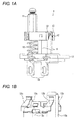
- FIG. 1A is a perspective view showing the configuration of the switching device 1.
- the switching device 1 is a switching device for industrial use, and is specifically a limit switch.
- the limit switch is used, for example, as a sensor for performing positioning or object detection in production equipment or an industrial machine.
- the switching device 1 is provided with a first movable unit 11, a movable contact (first contact) 12, a second movable unit 13, a terminal 14, a fixed contact (second contact) 15, a spring 16, and a terminal base 17.
- the first movable unit 11 is disposed on the spring 16. Further, the first movable unit 11 is integrally formed with the second movable unit 13. The first movable unit 11 and the second movable unit 13 are movable in a lengthwise direction of the figure.
- the movable contact 12 is fixed to the second movable unit 13.
- the movable contact 12 constitutes a switching mechanism for switching an electrical contact state by sliding against a surface of the fixed contact 15.
- Fig. 1B is a perspective view showing the movable contact 12 and the fixed contact 15 in an enlarged manner.
- the fixed contact 15 is made up of a first fixed contact 15b and a second fixed contact 15c.
- the movable contact 12 includes a first movable contact portion 12b that slides against the first fixed contact 15b, and a second movable contact portion 12c that slides against the second fixed contact 15c.
- the switching mechanism When the second fixed contact 15c and the second movable contact portion 12c are in contact with each other, the switching mechanism is in an on-state. When the second fixed contact 15c and the second movable contact portion 12c are separated from each other, the switching mechanism is in an off-state. In the state shown in Fig. 1B , the second fixed contact 15c and the second movable contact portion 12c are separated from each other, and hence the switching mechanism is in the off-state.
- the first fixed contact 15b and the first movable contact portion 12b are always in constant contact with each other irrespective of the position of the first movable unit 11. That is, the on or off switching of the switching mechanism is achieved by the contact or separation between the second fixed contact 15c and the second movable contact portion 12c.
- the terminal 14 connects the switching device 1 to external electrical wiring.
- the terminal 14 is disposed on a lower surface of the terminal base 17.
- the fixed contact 15 is disposed on an upper surface of the terminal base 17. That is, the fixed contact 15 is disposed on an opposite-side surface of the terminal base 17 to the surface thereof on which the terminal 14 is disposed.
- the spring 16 shrinks in the lengthwise direction by being applied with pressing force F (see Fig. 2A ) downward from above.
- the spring 16 extends to its original length (its length before application of the pressing force F) by being released from the pressing force F.
- the spring 16 is disposed on the upper surface of the terminal base 17.
- the spring 16 is specifically a hook spring.
- Fig. 2A shows a form of the switching device 1 in which the pressing force F is applied to the first movable unit 11, and Fig. 2B shows the movable contact 12 and the fixed contact 15 in an enlarged manner.
- the first movable unit 11 disposed on the spring 16, the second movable unit 13 integrally formed with the first movable unit 11, and the movable contact 12 fixed to the second movable unit 13 move downward from above. Then, as shown in Fig. 2B , the second fixed contact 15c and the second movable contact portion 12c begin to come into contact with each other. Thus, the switching mechanism comes into the on-state.
- the second movable contact portion 12c further moves downward while the second movable contact portion 12c and the second fixed contact 15c rub against each other.
- the first movable contact portion 12b is held in the state of being always in constant contact with the first fixed contact 15b, while sliding against a surface of the first fixed contact 15b.
- the pressing force F of pressing the first movable unit 11 stops being applied (or is reduced)
- the first movable unit 11, the movable contact 12, and the second movable unit 13 return to original positions thereof (positions thereof before the application of the pressing force F to the first movable unit 11) by elastic force of the spring 16.
- the second movable contact portion 12c moves upward while the second movable contact portion 12c and the second fixed contact 15c rub against each other, and is eventually separated from the second fixed contact 15c again.
- the switching mechanism comes back into the off-state.
- the first movable unit 11 may not be configured to be movable in the lengthwise direction.
- the first movable unit 11 may include an operation unit (e.g., a lever) that rotates and a slider that slides in the lengthwise direction in conjunction with rotation of the operation unit.
- the first movable unit 11 converts, on the inside of the first movable unit 11, the force of rotating the operation unit to the force of moving the slider in the lengthwise direction.
- the movable contact 12 is fixed to the slider of the first movable unit 11. By rotation of the operation unit and sliding of the slider in the lengthwise direction, the movable contact 12 also moves in the lengthwise direction.
- Fig. 3 is an enlarged view of a main part of the switching device 1 shown in Fig. 2A .
- the fixed contact 15 is coated with a hard plating layer 15a (outermost surface layer).
- a contact portion to come into contact with the movable contact 12 may only be coated with the hard plating layer 15a.
- the hard plating layer 15a desirably has a high Martens hardness of 132 mgf/ ⁇ m 2 (HM) or more.
- HM Martens hardness
- a range of the desirable Martens hardness of the hard plating layer 15a relies on a material for the hard plating layer 15a.
- a thickness of the hard plating layer 15a is preferably from 1 ⁇ m or more to 10 ⁇ m or less.
- the desirable thickness of the hard plating layer 15a relies on the material for the hard plating layer 15a (and the hardness of the material).
- the thickness of the hard plating layer 15a is preferably 1 ⁇ m or more.
- the thickness of the hard plating layer 15a is preferably 3 ⁇ m or more. This is because a friction characteristic of the hard plating layer 15a varies depending on the material, as will be described later.
- the Martens hardness and the thickness of the hard plating layer 15a are set such that the durable number of times of the fixed contact 15 is 10,000,000 or more (or at least 3,000,000 or more). The definition of the Martens hardness will be described later.
- the material for the hard plating layer 15a may be a noble metal, for example.
- the material for the hard plating layer 15a is preferably Ag (silver), Au (gold), Pd (palladium), Pt (platinum), or an alloy thereof.
- the hard plating layer 15a may be formed using a processing method of electroplating or non-electroplating.
- the fixed contact 15 may be coated with a surface layer, formed using a processing method of sputtering, vapor deposition, or lamination, in place of the hard plating layer 15a.
- the fixed contact 15 is coated with the hard plating layer 15a having high a Martens hardness, and thus has a larger durable number of times than that of the conventional sliding contact. Further, the fixed contact 15 has a "true contact area" which is the minimum contact area required for electrical conduction with the movable contact 12. Hence, the fixed contact 15 also holds high contact reliability, similarly to the conventional sliding contact. Accordingly, the fixed contact 15 can achieve both high durability and high contact reliability.
- the movable contact 12 is formed of a metal having a lower hardness than that of the hard plating layer 15a. That is, although abrasion occurs on the movable contact 12 due to sliding against the fixed contact 15, the movable contact 12 is kept by its elasticity in the state of being biased to and in contact with the fixed contact 15. Hence, the electrical connection between the movable contact 12 and the fixed contact 15 is held.
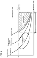
- FIG. 4 shows the correlation between a Martens hardness of the hard plating layer 15a made of Ag and a thickness of the hard plating layer 15a.
- Fig. 4 shows a range of the Martens hardness and thickness of the hard plating layer 15a which are required by a limit switch for industrial use. Further, Fig. 4 also shows a range of a Martens hardness and thickness of the conventional sliding contact.
- a "hardness upper limit” value may be set to such a value as to make the contact area between the movable contact 12 and the fixed contact 15 not excessively small (as not to significantly impair the contact reliability).
- the "hardness upper limit” value is preferably 300 mgf/ ⁇ m 2 (HM).
- a "thickness upper limit” value may be set in consideration of cost of the hard plating layer 15a. Since the material for the hard plating layer 15a is a noble metal, if the thickness is too large, the hard plating layer 15a would cost too high.
- the "thickness upper limit” value is preferably 10 ⁇ m.
- Fig. 4 also shows a graph representing the respective lower limit values of the Martens hardness and thickness of the hard plating layer 15a, which are required for the fixed contact 15 to achieve a target value of the durable number of times.
- the limit switch for industrial use requires the durable number of times of the fixed contact 15 to be about 10,000,000 or more.
- the hardness and thickness of the hard plating layer 15a are set such that the durable number of times of the fixed contact 15 coated with the hard plating layer 15a becomes about 10,000,000 or more.
- the fixed contact 15 can be applied to the limit switch.
- the durable number of times of the sliding contact according to the conventional design is about 1,000,000 or less. Thus, the conventional sliding contact cannot be applied to the limit switch.
- the thickness of the hard plating layer 15a needs to be 10 ⁇ m ("thickness upper limit" value) or more.
- the Martens hardness of the hard plating layer 15a needs to be set to 132 mgf/ ⁇ m 2 (HM) or more.
- the hardness and an abrasion loss of the hard plating layer 15a establish an inversely proportional relationship. For this reason, increasing the hardness of the hard plating layer 15a leads to improvement in durable number of times.
- the required thickness changes in accordance with the material for the hard plating layer 15a.
- the material for the hard plating layer 15a is Au
- the required thickness is about one-third of that in a case where the material for the hard plating layer 15a is Ag. This is because Ag and Au have different abrasion characteristics.
- the difference in abrasion characteristic depending on the material will be described later.
- the required thickness is smaller than 10 ⁇ m.
- the target value for the durable number of times of the fixed contact 15 is 100,000, the required thickness is even smaller. That is, the smaller (larger) the target value for the durable number of times, the smaller (larger) the required thickness. In other words, the smaller (larger) the target value for the durable number of times, the smaller (larger) the required Martens hardness.
- each hard plating layer 15a made of a material having the same hardness an abrasion loss of each hard plating layer 15a in one action of the movable contact 12, or some other characteristic
- the abrasion characteristic of the material for the hard plating layer 15a may vary depending on the material for the hard plating layer 15a. This is because behavior of an abrasion powder, fallen off the hard plating layer 15a due to abrasion, varies depending on the material for the hard plating layer 15a.
- a difference in abrasion characteristic between Ag and Au will be described.
- the material for the hard plating layer 15a is Au
- a composition of the abrasion powder hardly changes from that of Au.
- the abrasion powder is easily transferred back onto the surface (sliding surface) of the hard plating layer 15a which rubs against the movable contact 12.
- the abrasion powder of Au acts like a cushion between the hard plating layer 15a and the movable contact 12, thereby suppressing the progress of abrasion of the hard plating layer 15a.
- the hard plating layer 15a made of Au has the characteristic of hardly abrading. As a result, the durability of the fixed contact 15 coated with the hard plating layer 15a made of Au becomes high.
- the composition of the abrasion powder transforms by the effect of oxidation, sulfurization, or the like.
- grease molecules applied onto the sliding surface are easily adsorbed to the abrasion powder of Ag, as compared to the abrasion powder of Au. This makes the abrasion powder hardly transferred back onto the sliding surface.
- the abrasion powder of Ag acts like an abrasive between the movable contact 12 and the hard plating layer 15a with which the fixed contact 15 is coated, to promote abrasion of the hard plating layer 15a.
- the hard plating layer 15a made of Ag has the characteristic of easily abrading. As a result, the durability of the fixed contact 15 coated with the hard plating layer 15a made of Ag becomes relatively low.
- the material for the hard plating layer 15a when the material for the hard plating layer 15a is Au, the material can improve the durability of the fixed contact 15 as compared to the case in which the material for the hard plating layer 15a is Ag. In other words, when the material for the hard plating layer 15a is Au, the material can provide the durability (durable number of times) equivalent to that of the fixed contact 15 by having a small thickness, as compared to the case in which the material for the hard plating layer 15a is Ag.
- the Martens hardness is defined as the quotient ⁇ FMAX>/ ⁇ A(h)> obtained by dividing the maximum value ⁇ FMAX> of test force, applied to the surface of a sample by an indenter, by a surface area ⁇ A(h)> of a depression formed on the surface of the sample by the test force.
- the surface area ⁇ A(h)> of the depression is calculated from a depth ⁇ h> of the indenter pressed into the sample.
- indenters There exist two types of indenters, which are a Vickers indenter and a Berkovich indenter.
- the shape, size, and the like of the contact surface between the indenter and the sample vary depending on the type of the indenter, and a calculation formula for the surface area ⁇ A(h)> of the depression also varies.
- the basic definition of the Martens hardness is as described above, irrespective of the type of the indenter.
- the configuration has been described where the hard plating layer 15a with which the fixed contact 15 is coated has the Martens hardness of 132 mgf/ ⁇ m 2 or more.
- the "surface" of the fixed contact 15 may only have a high hardness of 132 mgf/ ⁇ m 2 or more.
- the "surface” of the fixed contact 15 means the surface on which the fixed contact 15 is in contact with the movable contact 12. Specifically, when the fixed contact 15 is coated (by plating or the like), the "surface” of the fixed contact 15 is the surface of the coating layer (the surface of the outermost surface layer when a plurality of coating layers are laminated). Meanwhile, when the fixed contact 15 is not coated, the "surface” of the fixed contact 15 is the surface of the fixed contact 15. Accordingly, the surface of the fixed contact 15 is not required to be coated with the coating layer or the like so long as the fixed contact 15 has a hardness of 132 mgf/ ⁇ m 2 or more.
- the fixed contact 15 may be formed of the same material (e.g., Au, Ag, Pd, Pt) as that for the hard plating layer 15a, and the surface of the fixed contact 15 may have a Martens hardness of 132 mgf/ ⁇ m 2 or more. According to this modification example, there is an advantage in that plating for coating the fixed contact 15 with the hard plating layer 15a is unnecessary.
- the invention can be applied to a switching device for industrial use, such as a limit switch.
Landscapes
- Chemical & Material Sciences (AREA)
- Engineering & Computer Science (AREA)
- Composite Materials (AREA)
- Materials Engineering (AREA)
- Contacts (AREA)
- Push-Button Switches (AREA)
Abstract
Description
- The invention relates to a switching device, and for example, relates to a switching device provided with a sliding contact.
- A switching device is provided with contacts for switching on and off of a switching mechanism. The contacts are schematically classified into two types: "sliding contacts" and "opposed contacts".
- The sliding contacts and the opposed contacts are different in action when switching operation for switching on and off of the switching mechanism is performed. That is, in a case where the switching operation for turning off the switching mechanism is performed when the switching mechanism is on (namely, when two contacts are in contact with each other), one sliding contact slides while being in contact with the other sliding contact. Meanwhile, in the same case, one opposed contact moves in a direction away from the other opposed contact.
- Since the opposed contacts and the sliding contacts are different in action when the switching operation is performed, those contacts are also different in durable number of times (durability) against the switching operation. Specifically, the durable number of times of the sliding contacts is approximately 300,000 to 1,000,000, for example. Meanwhile, the durable number of times of the opposed contacts is approximately tens of millions of times, for example. Therefore, the sliding contacts have been widely applied to switching devices for use in household electric appliances, automobiles and the like in which the number of times of actions by switching operation is small. Meanwhile, the opposed contacts have been applied to switching devices (e.g., limit switches) for industrial use in which the number of times of actions by switching operation is large.
-
JP 2007-326996 A JP 2000-3636 A - As compared to the opposed contacts, the sliding contacts have an advantage of having high contact reliability (low possibility to fail in coming into contact with the other opposed contact at the time of switching the switching mechanism from off to on). For this reason, the sliding contacts with higher reliability have been widely used in recent years. When the sliding contacts are adopted to the switching device for industrial use, malfunction of the switching device may hardly occur, the malfunction being caused by deterioration in ambient environment (generation of a corrosive gas, changes in temperature and humidity), contamination, or the like.
- However, the contacts in the switching device for industrial use (e.g., a small signal device) are required to have high durability (large durable number of times) against the switching operation. Specifically, the contacts in the switching device for industrial use are required to have a durable number of times of approximately 10,000,000. Sliding contacts having such a large durable number of times have not existed so far. Hence, it is not possible to apply the conventional sliding contacts to the switching device for industrial use.
- The invention has been made in view of the foregoing problem, and an object of the invention is to provide a switching device having both high durability and high contact reliability.
- In order to solve the above problem, a switching device according to the invention is a switching device which includes a first contact and a second contact and in which the first contact slides while being in contact with a surface of the second contact in switching a switching mechanism. On the surface, at least a contact portion to come into contact with the first contact has a Martens hardness of 132 mgf/µm2 or more.
- According to the above configuration, since the contact portion on the surface of the second contact has a high Martens hardness, the second contact has high durability. Further, since the first contact and the second contact are sliding contacts that slide in switching the switching mechanism, there is a low possibility for occurrence of malfunction caused by a corrosive gas, contamination, or the like, and the contact reliability is high. Hence, it is possible to achieve both high durability and high contact reliability.
- Further, in the switching device according to one aspect of the invention, on an outermost surface layer of the second contact, at least the contact portion to come into contact with the first contact may have a thickness from 1 µm or more to 10 µm or less.
- According to the above configuration, formation of the outermost surface layer (at least the contact portion) of the second contact by use of a material having high hardness enables achievement of a Martens hardness of 132 mgf/µm2 or more in the contact portion.
- Further, in the switching device according to one aspect of the invention, the contact portion may contain, as a material, any of silver, gold, palladium, platinum, and an alloy thereof.
- According to the above configuration, the contact portion contains, as the material, any of silver, gold, palladium, platinum, and an alloy thereof. Each of silver, gold, palladium, platinum, and an alloy thereof improves its hardness by being added with an additive. For example, silver improves its hardness by being added with a brightening agent containing Se (selenium) or Sb (antimony). Further, it is known that gold improves its hardness by being added with Ni (nickel) or Co (cobalt). Accordingly, by addition of an additive to the material at the time of processing of the contact portion, it is possible to achieve a Martens hardness of 132 mgf/µm2 or more in the contact portion after the processing.
- Further, in the switching device according to one aspect of the invention, the contact portion may have a Martens hardness of 300 mgf/µm2 or less.
- According to the above configuration, a true contact area between the first contact and the second contact does not become excessively small. Hence, it is possible to ensure sufficient electrical conductivity between the first contact and the second contact.
- Further, in the switching device according to one aspect of the invention, the outermost surface layer of the contact portion may be formed using any of processing methods of plating, sputtering, vapor deposition, and bonding.
- According to the above configuration, the outermost surface layer having a Martens hardness of 132 mgf/µm2 or more can be formed using any of well-known processing methods of plating, sputtering, vapor deposition, and bonding.
- According to the invention, it is possible to achieve both high durability and high contact reliability.
-
-
Figs. 1A and 1B are perspective views showing a configuration of a switching device according to one embodiment; -
Figs. 2A and 2B are perspective views showing a configuration of the switching device according to one embodiment in a case where pressing force is applied to the switching device; -
Fig. 3 is an enlarged view of a main part of the switching device shown inFig. 2A ; and -
Fig. 4 is a diagram showing the correlation between a Martens hardness of a surface of a fixed contact, provided in the switching device according to one embodiment, and a thickness of the hard plating. - Hereinafter, an embodiment of the invention will be described in detail.
- A configuration of a
switching device 1 according to the embodiment will be described with reference toFigs. 1A and 1B. Fig. 1A is a perspective view showing the configuration of theswitching device 1. In practice, at least part of theswitching device 1 is housed in a case, not shown. Theswitching device 1 is a switching device for industrial use, and is specifically a limit switch. The limit switch is used, for example, as a sensor for performing positioning or object detection in production equipment or an industrial machine. - As shown in
Fig. 1A , theswitching device 1 is provided with a firstmovable unit 11, a movable contact (first contact) 12, a secondmovable unit 13, aterminal 14, a fixed contact (second contact) 15, aspring 16, and aterminal base 17. - The first
movable unit 11 is disposed on thespring 16. Further, the firstmovable unit 11 is integrally formed with the secondmovable unit 13. The firstmovable unit 11 and the secondmovable unit 13 are movable in a lengthwise direction of the figure. - The
movable contact 12 is fixed to the secondmovable unit 13. Themovable contact 12 constitutes a switching mechanism for switching an electrical contact state by sliding against a surface of the fixedcontact 15. -
Fig. 1B is a perspective view showing themovable contact 12 and the fixedcontact 15 in an enlarged manner. As shown inFig. 1B , the fixedcontact 15 is made up of a firstfixed contact 15b and a second fixedcontact 15c. Further, themovable contact 12 includes a firstmovable contact portion 12b that slides against the firstfixed contact 15b, and a secondmovable contact portion 12c that slides against the second fixedcontact 15c. - When the second fixed
contact 15c and the secondmovable contact portion 12c are in contact with each other, the switching mechanism is in an on-state. When the second fixedcontact 15c and the secondmovable contact portion 12c are separated from each other, the switching mechanism is in an off-state. In the state shown inFig. 1B , the second fixedcontact 15c and the secondmovable contact portion 12c are separated from each other, and hence the switching mechanism is in the off-state. - The first
fixed contact 15b and the firstmovable contact portion 12b are always in constant contact with each other irrespective of the position of the firstmovable unit 11. That is, the on or off switching of the switching mechanism is achieved by the contact or separation between the second fixedcontact 15c and the secondmovable contact portion 12c. - The terminal 14 connects the
switching device 1 to external electrical wiring. The terminal 14 is disposed on a lower surface of theterminal base 17. - The fixed
contact 15 is disposed on an upper surface of theterminal base 17. That is, the fixedcontact 15 is disposed on an opposite-side surface of theterminal base 17 to the surface thereof on which the terminal 14 is disposed. - The
spring 16 shrinks in the lengthwise direction by being applied with pressing force F (seeFig. 2A ) downward from above. Thespring 16 extends to its original length (its length before application of the pressing force F) by being released from the pressing force F. Similarly to the fixedcontact 15, thespring 16 is disposed on the upper surface of theterminal base 17. Thespring 16 is specifically a hook spring. - An action of the
switching device 1 will be schematically described with reference toFigs. 1A ,1B, 2A , and2B. Fig. 2A shows a form of theswitching device 1 in which the pressing force F is applied to the firstmovable unit 11, andFig. 2B shows themovable contact 12 and the fixedcontact 15 in an enlarged manner. - In a state where the pressing force F is not applied, as shown in
Figs. 1A and 1B , the second fixedcontact 15c and the secondmovable contact portion 12c are separated from each other, and the switching mechanism is in the off-state. - As shown in
Fig. 2A , when the pressing force F is applied to the firstmovable unit 11 and the secondmovable unit 13 downward from above, the pressing force F is applied to thespring 16 via the firstmovable unit 11. Thespring 16 applied with the pressing force F shrinks in the lengthwise direction. - With the shrinkage of the
spring 16 in the lengthwise direction, the firstmovable unit 11 disposed on thespring 16, the secondmovable unit 13 integrally formed with the firstmovable unit 11, and themovable contact 12 fixed to the secondmovable unit 13 move downward from above. Then, as shown inFig. 2B , the second fixedcontact 15c and the secondmovable contact portion 12c begin to come into contact with each other. Thus, the switching mechanism comes into the on-state. When the pressing force F is further applied, the secondmovable contact portion 12c further moves downward while the secondmovable contact portion 12c and the second fixedcontact 15c rub against each other. During this time, the firstmovable contact portion 12b is held in the state of being always in constant contact with the firstfixed contact 15b, while sliding against a surface of the firstfixed contact 15b. - When the pressing force F of pressing the first
movable unit 11 stops being applied (or is reduced), the firstmovable unit 11, themovable contact 12, and the secondmovable unit 13 return to original positions thereof (positions thereof before the application of the pressing force F to the first movable unit 11) by elastic force of thespring 16. Then, the secondmovable contact portion 12c moves upward while the secondmovable contact portion 12c and the second fixedcontact 15c rub against each other, and is eventually separated from the second fixedcontact 15c again. Thus, the switching mechanism comes back into the off-state. - The first
movable unit 11 may not be configured to be movable in the lengthwise direction. For example, the firstmovable unit 11 may include an operation unit (e.g., a lever) that rotates and a slider that slides in the lengthwise direction in conjunction with rotation of the operation unit. In this configuration, when the operation of rotating the operation unit is performed, the firstmovable unit 11 converts, on the inside of the firstmovable unit 11, the force of rotating the operation unit to the force of moving the slider in the lengthwise direction. Themovable contact 12 is fixed to the slider of the firstmovable unit 11. By rotation of the operation unit and sliding of the slider in the lengthwise direction, themovable contact 12 also moves in the lengthwise direction. -
Fig. 3 is an enlarged view of a main part of theswitching device 1 shown inFig. 2A . As shown inFig. 3 , the fixedcontact 15 is coated with ahard plating layer 15a (outermost surface layer). On the fixedcontact 15, at least a contact portion to come into contact with themovable contact 12 may only be coated with thehard plating layer 15a. - The
hard plating layer 15a desirably has a high Martens hardness of 132 mgf/µm2 (HM) or more. However, a range of the desirable Martens hardness of thehard plating layer 15a relies on a material for thehard plating layer 15a. Further, a thickness of thehard plating layer 15a is preferably from 1 µm or more to 10 µm or less. However, the desirable thickness of thehard plating layer 15a relies on the material for thehard plating layer 15a (and the hardness of the material). For example, when the material for thehard plating layer 15a is Au or Pd, the thickness of thehard plating layer 15a is preferably 1 µm or more. When the material for thehard plating layer 15a is Ag, the thickness of thehard plating layer 15a is preferably 3 µm or more. This is because a friction characteristic of thehard plating layer 15a varies depending on the material, as will be described later. As will be described below, the Martens hardness and the thickness of thehard plating layer 15a are set such that the durable number of times of the fixedcontact 15 is 10,000,000 or more (or at least 3,000,000 or more). The definition of the Martens hardness will be described later. - The material for the
hard plating layer 15a may be a noble metal, for example. In particular, the material for thehard plating layer 15a is preferably Ag (silver), Au (gold), Pd (palladium), Pt (platinum), or an alloy thereof. In these configurations, thehard plating layer 15a may be formed using a processing method of electroplating or non-electroplating. - Alternatively, in one modification example, the fixed
contact 15 may be coated with a surface layer, formed using a processing method of sputtering, vapor deposition, or lamination, in place of thehard plating layer 15a. - As described above, the fixed
contact 15 is coated with thehard plating layer 15a having high a Martens hardness, and thus has a larger durable number of times than that of the conventional sliding contact. Further, the fixedcontact 15 has a "true contact area" which is the minimum contact area required for electrical conduction with themovable contact 12. Hence, the fixedcontact 15 also holds high contact reliability, similarly to the conventional sliding contact. Accordingly, the fixedcontact 15 can achieve both high durability and high contact reliability. - The
movable contact 12 is formed of a metal having a lower hardness than that of thehard plating layer 15a. That is, although abrasion occurs on themovable contact 12 due to sliding against the fixedcontact 15, themovable contact 12 is kept by its elasticity in the state of being biased to and in contact with the fixedcontact 15. Hence, the electrical connection between themovable contact 12 and the fixedcontact 15 is held. - A method for setting the hardness and thickness of the
hard plating layer 15a will be described with reference toFig. 4 . Herein, the material for thehard plating layer 15a is assumed to be Ag.Fig. 4 shows the correlation between a Martens hardness of thehard plating layer 15a made of Ag and a thickness of thehard plating layer 15a. -
Fig. 4 shows a range of the Martens hardness and thickness of thehard plating layer 15a which are required by a limit switch for industrial use. Further,Fig. 4 also shows a range of a Martens hardness and thickness of the conventional sliding contact. InFig. 4 , a "hardness upper limit" value may be set to such a value as to make the contact area between themovable contact 12 and the fixedcontact 15 not excessively small (as not to significantly impair the contact reliability). Specifically, the "hardness upper limit" value is preferably 300 mgf/µm2 (HM). Further, a "thickness upper limit" value may be set in consideration of cost of thehard plating layer 15a. Since the material for thehard plating layer 15a is a noble metal, if the thickness is too large, thehard plating layer 15a would cost too high. Specifically, the "thickness upper limit" value is preferably 10 µm. - Further,
Fig. 4 also shows a graph representing the respective lower limit values of the Martens hardness and thickness of thehard plating layer 15a, which are required for the fixedcontact 15 to achieve a target value of the durable number of times. - As shown in
Fig. 4 , the limit switch for industrial use requires the durable number of times of the fixedcontact 15 to be about 10,000,000 or more. The hardness and thickness of thehard plating layer 15a are set such that the durable number of times of the fixedcontact 15 coated with thehard plating layer 15a becomes about 10,000,000 or more. Thus, the fixedcontact 15 can be applied to the limit switch. On the other hand, as shown inFig. 4 , the durable number of times of the sliding contact according to the conventional design is about 1,000,000 or less. Thus, the conventional sliding contact cannot be applied to the limit switch. - As shown in
Fig. 4 , when the target value for the durable number of times of the fixedcontact 15 is 10,000,000, and when the hardness of thehard plating layer 15a is 132 mgf/µm2 (HM), the thickness of thehard plating layer 15a needs to be 10 µm ("thickness upper limit" value) or more. Conversely, for setting the thickness of thehard plating layer 15a to 10 µm or less, the Martens hardness of thehard plating layer 15a needs to be set to 132 mgf/µm2 (HM) or more. Herein, the hardness and an abrasion loss of thehard plating layer 15a establish an inversely proportional relationship. For this reason, increasing the hardness of thehard plating layer 15a leads to improvement in durable number of times. - The required thickness changes in accordance with the material for the
hard plating layer 15a. For example, when the material for thehard plating layer 15a is Au, the required thickness is about one-third of that in a case where the material for thehard plating layer 15a is Ag. This is because Ag and Au have different abrasion characteristics. The more easily (hardly) the material used for thehard plating layer 15a abrades, the larger (smaller) the thickness required for achieving the target value for the durable number of times of the fixedcontact 15. The difference in abrasion characteristic depending on the material will be described later. - As will be seen from
Fig. 4 , when the target value for the durable number of times of thehard plating layer 15a is 1,000,000 and the Martens hardness of thehard plating layer 15a is 132 mgf/µm2 (HM), the required thickness is smaller than 10 µm. Further, when the target value for the durable number of times of the fixedcontact 15 is 100,000, the required thickness is even smaller. That is, the smaller (larger) the target value for the durable number of times, the smaller (larger) the required thickness. In other words, the smaller (larger) the target value for the durable number of times, the smaller (larger) the required Martens hardness. - It is generally thought that the abrasion characteristic of each
hard plating layer 15a made of a material having the same hardness (an abrasion loss of eachhard plating layer 15a in one action of themovable contact 12, or some other characteristic) is the same. However, in practice, the abrasion characteristic of the material for thehard plating layer 15a may vary depending on the material for thehard plating layer 15a. This is because behavior of an abrasion powder, fallen off thehard plating layer 15a due to abrasion, varies depending on the material for thehard plating layer 15a. Herein, as one example, a difference in abrasion characteristic between Ag and Au will be described. - As well known, Au is chemically highly stable. For this reason, when the material for the
hard plating layer 15a is Au, a composition of the abrasion powder hardly changes from that of Au. Hence, the abrasion powder is easily transferred back onto the surface (sliding surface) of thehard plating layer 15a which rubs against themovable contact 12. Additionally, the abrasion powder of Au acts like a cushion between thehard plating layer 15a and themovable contact 12, thereby suppressing the progress of abrasion of thehard plating layer 15a. - Accordingly, the
hard plating layer 15a made of Au has the characteristic of hardly abrading. As a result, the durability of the fixedcontact 15 coated with thehard plating layer 15a made of Au becomes high. - Meanwhile, Ag corrodes by an effect of oxidation, sulfurization, or the like. Thus, when the material for the
hard plating layer 15a is Ag, the composition of the abrasion powder transforms by the effect of oxidation, sulfurization, or the like. Further, grease molecules applied onto the sliding surface are easily adsorbed to the abrasion powder of Ag, as compared to the abrasion powder of Au. This makes the abrasion powder hardly transferred back onto the sliding surface. Further, the abrasion powder of Ag acts like an abrasive between themovable contact 12 and thehard plating layer 15a with which the fixedcontact 15 is coated, to promote abrasion of thehard plating layer 15a. - Accordingly, the
hard plating layer 15a made of Ag has the characteristic of easily abrading. As a result, the durability of the fixedcontact 15 coated with thehard plating layer 15a made of Ag becomes relatively low. - As described above, when the material for the
hard plating layer 15a is Au, the material can improve the durability of the fixedcontact 15 as compared to the case in which the material for thehard plating layer 15a is Ag. In other words, when the material for thehard plating layer 15a is Au, the material can provide the durability (durable number of times) equivalent to that of the fixedcontact 15 by having a small thickness, as compared to the case in which the material for thehard plating layer 15a is Ag. - The Martens hardness is defined as the quotient <FMAX>/<A(h)> obtained by dividing the maximum value <FMAX> of test force, applied to the surface of a sample by an indenter, by a surface area <A(h)> of a depression formed on the surface of the sample by the test force. Herein, the surface area <A(h)> of the depression is calculated from a depth <h> of the indenter pressed into the sample.
- There exist two types of indenters, which are a Vickers indenter and a Berkovich indenter. The shape, size, and the like of the contact surface between the indenter and the sample vary depending on the type of the indenter, and a calculation formula for the surface area <A(h)> of the depression also varies. However, the basic definition of the Martens hardness is as described above, irrespective of the type of the indenter.
- In the embodiment, the configuration has been described where the
hard plating layer 15a with which the fixedcontact 15 is coated has the Martens hardness of 132 mgf/µm2 or more. However, in the invention, the "surface" of the fixedcontact 15 may only have a high hardness of 132 mgf/µm2 or more. The "surface" of the fixedcontact 15 means the surface on which the fixedcontact 15 is in contact with themovable contact 12. Specifically, when the fixedcontact 15 is coated (by plating or the like), the "surface" of the fixedcontact 15 is the surface of the coating layer (the surface of the outermost surface layer when a plurality of coating layers are laminated). Meanwhile, when the fixedcontact 15 is not coated, the "surface" of the fixedcontact 15 is the surface of the fixedcontact 15. Accordingly, the surface of the fixedcontact 15 is not required to be coated with the coating layer or the like so long as the fixedcontact 15 has a hardness of 132 mgf/µm2 or more. - For example, in one modification example, the fixed
contact 15 may be formed of the same material (e.g., Au, Ag, Pd, Pt) as that for thehard plating layer 15a, and the surface of the fixedcontact 15 may have a Martens hardness of 132 mgf/µm2 or more. According to this modification example, there is an advantage in that plating for coating the fixedcontact 15 with thehard plating layer 15a is unnecessary. - The invention is not restricted to the foregoing embodiment, and a variety of modifications can be made in the scope of the claims.
- The invention can be applied to a switching device for industrial use, such as a limit switch.
Claims (5)
- A switching device (1) comprising a first contact (12) and a second contact (15), the first contact (12) sliding while being in contact with a surface of the second contact (15) in switching a switching mechanism,
the switching device (1) characterized in that
on the surface, at least a contact portion to come into contact with the first contact (12) has a Martens hardness of 132 mgf/µm2 or more. - The switching device (1) according to claim 1, characterized in that, on an outermost surface layer (15a) of the second contact (15), at least the contact portion to come into contact with the first contact (12) has a thickness from 1 µm or more to 10 µm or less.
- The switching device (1) according to claim 1 or 2, characterized in that the contact portion contains, as a material, any of silver, gold, palladium, platinum, and an alloy thereof.
- The switching device (1) according to any one of claims 1 to 3, characterized in that the contact portion has a Martens hardness of 300 mgf/µm2 or less.
- The switching device (1) according to any of claims 2 to 4, characterized in that the outermost surface layer (15a) of the contact portion is formed using any of processing methods of plating, sputtering, vapor deposition, and bonding.
Applications Claiming Priority (1)
| Application Number | Priority Date | Filing Date | Title |
|---|---|---|---|
| JP2015049766A JP2016170967A (en) | 2015-03-12 | 2015-03-12 | Switch gear |
Publications (1)
| Publication Number | Publication Date |
|---|---|
| EP3067908A1 true EP3067908A1 (en) | 2016-09-14 |
Family
ID=55486573
Family Applications (1)
| Application Number | Title | Priority Date | Filing Date |
|---|---|---|---|
| EP16159072.4A Withdrawn EP3067908A1 (en) | 2015-03-12 | 2016-03-08 | Switching device |
Country Status (4)
| Country | Link |
|---|---|
| US (1) | US20160268067A1 (en) |
| EP (1) | EP3067908A1 (en) |
| JP (1) | JP2016170967A (en) |
| CN (1) | CN105977063A (en) |
Cited By (1)
| Publication number | Priority date | Publication date | Assignee | Title |
|---|---|---|---|---|
| EP4333008A1 (en) * | 2022-08-31 | 2024-03-06 | Tanaka Kikinzoku Kogyo K.K. | Contact member for micro-load switching contact |
Families Citing this family (2)
| Publication number | Priority date | Publication date | Assignee | Title |
|---|---|---|---|---|
| JP2017162671A (en) * | 2016-03-09 | 2017-09-14 | オムロン株式会社 | Limit switch device |
| JP6729360B2 (en) * | 2016-12-27 | 2020-07-22 | オムロン株式会社 | switch |
Citations (6)
| Publication number | Priority date | Publication date | Assignee | Title |
|---|---|---|---|---|
| US3566056A (en) * | 1968-12-12 | 1971-02-23 | Mc Graw Edison Co | Air disconnect switch |
| JP2000003636A (en) | 1998-06-15 | 2000-01-07 | Omron Corp | Limit switch |
| US6432157B1 (en) * | 1999-04-23 | 2002-08-13 | Tanaka Kikinzoku Kogyo K.K. | Method for preparing Ag-ZnO electric contact material and electric contact material produced thereby |
| JP2007326996A (en) | 2006-06-09 | 2007-12-20 | Alps Electric Co Ltd | Lubricating composition for electrical contacts |
| US20080308395A1 (en) * | 2007-06-18 | 2008-12-18 | Motoyoshi Murakami | Switch |
| EP2386784A1 (en) * | 2010-05-13 | 2011-11-16 | Delta Kogyo Co., Ltd. | Slide switch |
-
2015
- 2015-03-12 JP JP2015049766A patent/JP2016170967A/en not_active Abandoned
-
2016
- 2016-03-01 US US15/057,449 patent/US20160268067A1/en not_active Abandoned
- 2016-03-08 EP EP16159072.4A patent/EP3067908A1/en not_active Withdrawn
- 2016-03-11 CN CN201610137461.2A patent/CN105977063A/en active Pending
Patent Citations (6)
| Publication number | Priority date | Publication date | Assignee | Title |
|---|---|---|---|---|
| US3566056A (en) * | 1968-12-12 | 1971-02-23 | Mc Graw Edison Co | Air disconnect switch |
| JP2000003636A (en) | 1998-06-15 | 2000-01-07 | Omron Corp | Limit switch |
| US6432157B1 (en) * | 1999-04-23 | 2002-08-13 | Tanaka Kikinzoku Kogyo K.K. | Method for preparing Ag-ZnO electric contact material and electric contact material produced thereby |
| JP2007326996A (en) | 2006-06-09 | 2007-12-20 | Alps Electric Co Ltd | Lubricating composition for electrical contacts |
| US20080308395A1 (en) * | 2007-06-18 | 2008-12-18 | Motoyoshi Murakami | Switch |
| EP2386784A1 (en) * | 2010-05-13 | 2011-11-16 | Delta Kogyo Co., Ltd. | Slide switch |
Non-Patent Citations (1)
| Title |
|---|
| ERHARD REIMANN: "Martens Hardness -More Than Just Hardness Testing", 26 September 2002 (2002-09-26), XP055288230, Retrieved from the Internet <URL:http://www.imeko.org/publications/tc5-2002/IMEKO-TC5-2002-029.pdf> [retrieved on 20160713] * |
Cited By (1)
| Publication number | Priority date | Publication date | Assignee | Title |
|---|---|---|---|---|
| EP4333008A1 (en) * | 2022-08-31 | 2024-03-06 | Tanaka Kikinzoku Kogyo K.K. | Contact member for micro-load switching contact |
Also Published As
| Publication number | Publication date |
|---|---|
| CN105977063A (en) | 2016-09-28 |
| US20160268067A1 (en) | 2016-09-15 |
| JP2016170967A (en) | 2016-09-23 |
Similar Documents
| Publication | Publication Date | Title |
|---|---|---|
| US9984840B2 (en) | Keyswitch structure, switch structure and method of assembling a keyswitch structure | |
| US20160268067A1 (en) | Switching device | |
| JP5334416B2 (en) | Electrical contact and socket for electrical parts | |
| EP2978076B1 (en) | Electrical connector, and socket for electric component | |
| CN107026338B (en) | Terminal pair and connector | |
| JP3889718B2 (en) | Metal plate used for electrical contact and method for manufacturing the same | |
| CN107924771B (en) | Contact member, sliding contact, electrical equipment, and method of manufacturing the contact member | |
| JP7113133B2 (en) | Operating device | |
| US20080308395A1 (en) | Switch | |
| US7235750B1 (en) | Radio frequency MEMS switch contact metal selection | |
| CN104282457B (en) | Switchgear, manufacturing method of leaf spring, and leaf spring | |
| CN102308352A (en) | Sliding contact assembly | |
| WO2020236497A1 (en) | Substrate sticking and breakage mitigation | |
| EP3035356B1 (en) | Electrical switches and methods | |
| TWI697155B (en) | Electrical connector and socket for electrical component | |
| JP2017103088A (en) | switch | |
| CN108231439B (en) | Electrical contact material | |
| US5826706A (en) | Contact mechanism for a switch | |
| US3283106A (en) | Electrical contact elements | |
| JP2003249151A (en) | Multi-directional operation switch | |
| US20160141118A1 (en) | Limit switch | |
| WO2012168105A1 (en) | Manufacturing method for a sliding contact assembly | |
| CN101887825B (en) | Breaker | |
| JP2002334628A (en) | Push-on switch | |
| JP6579425B2 (en) | Board switch |
Legal Events
| Date | Code | Title | Description |
|---|---|---|---|
| PUAI | Public reference made under article 153(3) epc to a published international application that has entered the european phase |
Free format text: ORIGINAL CODE: 0009012 |
|
| 17P | Request for examination filed |
Effective date: 20160308 |
|
| AK | Designated contracting states |
Kind code of ref document: A1 Designated state(s): AL AT BE BG CH CY CZ DE DK EE ES FI FR GB GR HR HU IE IS IT LI LT LU LV MC MK MT NL NO PL PT RO RS SE SI SK SM TR |
|
| AX | Request for extension of the european patent |
Extension state: BA ME |
|
| STAA | Information on the status of an ep patent application or granted ep patent |
Free format text: STATUS: EXAMINATION IS IN PROGRESS |
|
| STAA | Information on the status of an ep patent application or granted ep patent |
Free format text: STATUS: THE APPLICATION HAS BEEN WITHDRAWN |
|
| 17Q | First examination report despatched |
Effective date: 20170504 |
|
| 18W | Application withdrawn |
Effective date: 20170523 |