EP3067693A1 - Nanopore forming method and uses thereof - Google Patents
Nanopore forming method and uses thereof Download PDFInfo
- Publication number
- EP3067693A1 EP3067693A1 EP15158894.4A EP15158894A EP3067693A1 EP 3067693 A1 EP3067693 A1 EP 3067693A1 EP 15158894 A EP15158894 A EP 15158894A EP 3067693 A1 EP3067693 A1 EP 3067693A1
- Authority
- EP
- European Patent Office
- Prior art keywords
- nanopore
- tmdc
- mos
- membrane
- pore
- Prior art date
- Legal status (The legal status is an assumption and is not a legal conclusion. Google has not performed a legal analysis and makes no representation as to the accuracy of the status listed.)
- Withdrawn
Links
- 238000000034 method Methods 0.000 title claims abstract description 85
- 239000012528 membrane Substances 0.000 claims abstract description 87
- 239000011148 porous material Substances 0.000 claims abstract description 83
- 150000003624 transition metals Chemical class 0.000 claims abstract description 32
- 229910052723 transition metal Inorganic materials 0.000 claims abstract description 30
- CWQXQMHSOZUFJS-UHFFFAOYSA-N molybdenum disulfide Chemical compound S=[Mo]=S CWQXQMHSOZUFJS-UHFFFAOYSA-N 0.000 claims description 79
- 239000010410 layer Substances 0.000 claims description 66
- 239000007788 liquid Substances 0.000 claims description 34
- 239000002356 single layer Substances 0.000 claims description 23
- 238000004519 manufacturing process Methods 0.000 claims description 21
- 230000003647 oxidation Effects 0.000 claims description 15
- 238000007254 oxidation reaction Methods 0.000 claims description 15
- XLYOFNOQVPJJNP-UHFFFAOYSA-N water Substances O XLYOFNOQVPJJNP-UHFFFAOYSA-N 0.000 claims description 9
- 229910021607 Silver chloride Inorganic materials 0.000 claims description 8
- HKZLPVFGJNLROG-UHFFFAOYSA-M silver monochloride Chemical compound [Cl-].[Ag+] HKZLPVFGJNLROG-UHFFFAOYSA-M 0.000 claims description 8
- 229910001868 water Inorganic materials 0.000 claims description 6
- TWRXJAOTZQYOKJ-UHFFFAOYSA-L Magnesium chloride Chemical compound [Mg+2].[Cl-].[Cl-] TWRXJAOTZQYOKJ-UHFFFAOYSA-L 0.000 claims description 4
- -1 SnSe2 Chemical compound 0.000 claims description 4
- FAPWRFPIFSIZLT-UHFFFAOYSA-M Sodium chloride Chemical compound [Na+].[Cl-] FAPWRFPIFSIZLT-UHFFFAOYSA-M 0.000 claims description 4
- 239000013078 crystal Substances 0.000 claims description 4
- 239000003792 electrolyte Substances 0.000 claims description 4
- 238000005530 etching Methods 0.000 claims description 4
- KWGKDLIKAYFUFQ-UHFFFAOYSA-M lithium chloride Chemical compound [Li+].[Cl-] KWGKDLIKAYFUFQ-UHFFFAOYSA-M 0.000 claims description 4
- 150000003839 salts Chemical class 0.000 claims description 4
- 239000000126 substance Substances 0.000 claims description 4
- 229910052717 sulfur Inorganic materials 0.000 claims description 4
- UXVMQQNJUSDDNG-UHFFFAOYSA-L Calcium chloride Chemical compound [Cl-].[Cl-].[Ca+2] UXVMQQNJUSDDNG-UHFFFAOYSA-L 0.000 claims description 2
- 229910003090 WSe2 Inorganic materials 0.000 claims description 2
- 239000001110 calcium chloride Substances 0.000 claims description 2
- 229910001628 calcium chloride Inorganic materials 0.000 claims description 2
- 229910052798 chalcogen Inorganic materials 0.000 claims description 2
- 150000001787 chalcogens Chemical group 0.000 claims description 2
- 229910001629 magnesium chloride Inorganic materials 0.000 claims description 2
- 229910052711 selenium Inorganic materials 0.000 claims description 2
- 239000011780 sodium chloride Substances 0.000 claims description 2
- 229910052961 molybdenite Inorganic materials 0.000 claims 3
- 229910052982 molybdenum disulfide Inorganic materials 0.000 claims 3
- 230000015572 biosynthetic process Effects 0.000 abstract description 44
- 238000012544 monitoring process Methods 0.000 abstract description 6
- 238000003487 electrochemical reaction Methods 0.000 description 34
- 230000008569 process Effects 0.000 description 27
- WCUXLLCKKVVCTQ-UHFFFAOYSA-M Potassium chloride Chemical compound [Cl-].[K+] WCUXLLCKKVVCTQ-UHFFFAOYSA-M 0.000 description 17
- OKTJSMMVPCPJKN-UHFFFAOYSA-N Carbon Chemical compound [C] OKTJSMMVPCPJKN-UHFFFAOYSA-N 0.000 description 15
- 229910021389 graphene Inorganic materials 0.000 description 15
- 230000005945 translocation Effects 0.000 description 15
- 229910004205 SiNX Inorganic materials 0.000 description 11
- 125000004429 atom Chemical group 0.000 description 11
- 238000005229 chemical vapour deposition Methods 0.000 description 11
- 238000011065 in-situ storage Methods 0.000 description 10
- 230000007547 defect Effects 0.000 description 9
- 239000000463 material Substances 0.000 description 9
- 239000001103 potassium chloride Substances 0.000 description 8
- 235000011164 potassium chloride Nutrition 0.000 description 8
- 230000008901 benefit Effects 0.000 description 7
- 238000003917 TEM image Methods 0.000 description 6
- 238000005259 measurement Methods 0.000 description 6
- 229920003229 poly(methyl methacrylate) Polymers 0.000 description 6
- 239000004926 polymethyl methacrylate Substances 0.000 description 6
- 239000011829 room temperature ionic liquid solvent Substances 0.000 description 6
- 229910052594 sapphire Inorganic materials 0.000 description 6
- 239000010980 sapphire Substances 0.000 description 6
- 238000004458 analytical method Methods 0.000 description 5
- 230000015556 catabolic process Effects 0.000 description 5
- 238000004090 dissolution Methods 0.000 description 5
- 230000005684 electric field Effects 0.000 description 5
- 229910052750 molybdenum Inorganic materials 0.000 description 5
- 239000000758 substrate Substances 0.000 description 5
- 238000012546 transfer Methods 0.000 description 5
- XKRFYHLGVUSROY-UHFFFAOYSA-N Argon Chemical compound [Ar] XKRFYHLGVUSROY-UHFFFAOYSA-N 0.000 description 4
- LFQSCWFLJHTTHZ-UHFFFAOYSA-N Ethanol Chemical compound CCO LFQSCWFLJHTTHZ-UHFFFAOYSA-N 0.000 description 4
- 239000011521 glass Substances 0.000 description 4
- 238000010884 ion-beam technique Methods 0.000 description 4
- 239000000203 mixture Substances 0.000 description 4
- JKQOBWVOAYFWKG-UHFFFAOYSA-N molybdenum trioxide Chemical compound O=[Mo](=O)=O JKQOBWVOAYFWKG-UHFFFAOYSA-N 0.000 description 4
- 230000003287 optical effect Effects 0.000 description 4
- 239000010453 quartz Substances 0.000 description 4
- VYPSYNLAJGMNEJ-UHFFFAOYSA-N silicon dioxide Inorganic materials O=[Si]=O VYPSYNLAJGMNEJ-UHFFFAOYSA-N 0.000 description 4
- 125000004434 sulfur atom Chemical group 0.000 description 4
- RYGMFSIKBFXOCR-UHFFFAOYSA-N Copper Chemical compound [Cu] RYGMFSIKBFXOCR-UHFFFAOYSA-N 0.000 description 3
- 229910052581 Si3N4 Inorganic materials 0.000 description 3
- 230000004075 alteration Effects 0.000 description 3
- 230000005540 biological transmission Effects 0.000 description 3
- 238000001514 detection method Methods 0.000 description 3
- 238000009826 distribution Methods 0.000 description 3
- 238000002149 energy-dispersive X-ray emission spectroscopy Methods 0.000 description 3
- 238000002474 experimental method Methods 0.000 description 3
- 239000013612 plasmid Substances 0.000 description 3
- 238000002360 preparation method Methods 0.000 description 3
- 108090000623 proteins and genes Proteins 0.000 description 3
- 102000004169 proteins and genes Human genes 0.000 description 3
- HQVNEWCFYHHQES-UHFFFAOYSA-N silicon nitride Chemical compound N12[Si]34N5[Si]62N3[Si]51N64 HQVNEWCFYHHQES-UHFFFAOYSA-N 0.000 description 3
- 239000000243 solution Substances 0.000 description 3
- CSCPPACGZOOCGX-UHFFFAOYSA-N Acetone Chemical compound CC(C)=O CSCPPACGZOOCGX-UHFFFAOYSA-N 0.000 description 2
- KFZMGEQAYNKOFK-UHFFFAOYSA-N Isopropanol Chemical compound CC(C)O KFZMGEQAYNKOFK-UHFFFAOYSA-N 0.000 description 2
- PNEYBMLMFCGWSK-UHFFFAOYSA-N aluminium oxide Inorganic materials [O-2].[O-2].[O-2].[Al+3].[Al+3] PNEYBMLMFCGWSK-UHFFFAOYSA-N 0.000 description 2
- 239000012062 aqueous buffer Substances 0.000 description 2
- 229910052786 argon Inorganic materials 0.000 description 2
- 238000004630 atomic force microscopy Methods 0.000 description 2
- 239000013590 bulk material Substances 0.000 description 2
- 125000004432 carbon atom Chemical group C* 0.000 description 2
- 238000006243 chemical reaction Methods 0.000 description 2
- 239000011889 copper foil Substances 0.000 description 2
- 229910052593 corundum Inorganic materials 0.000 description 2
- 238000007405 data analysis Methods 0.000 description 2
- 239000004205 dimethyl polysiloxane Substances 0.000 description 2
- 238000011049 filling Methods 0.000 description 2
- CJNBYAVZURUTKZ-UHFFFAOYSA-N hafnium(IV) oxide Inorganic materials O=[Hf]=O CJNBYAVZURUTKZ-UHFFFAOYSA-N 0.000 description 2
- 238000010952 in-situ formation Methods 0.000 description 2
- 230000003993 interaction Effects 0.000 description 2
- 229910052751 metal Inorganic materials 0.000 description 2
- 239000002184 metal Substances 0.000 description 2
- VNWKTOKETHGBQD-UHFFFAOYSA-N methane Chemical compound C VNWKTOKETHGBQD-UHFFFAOYSA-N 0.000 description 2
- 239000002086 nanomaterial Substances 0.000 description 2
- 239000002773 nucleotide Substances 0.000 description 2
- 125000003729 nucleotide group Chemical group 0.000 description 2
- 238000005424 photoluminescence Methods 0.000 description 2
- 229920000435 poly(dimethylsiloxane) Polymers 0.000 description 2
- 238000012552 review Methods 0.000 description 2
- 238000004088 simulation Methods 0.000 description 2
- 238000004513 sizing Methods 0.000 description 2
- 239000007787 solid Substances 0.000 description 2
- 238000012360 testing method Methods 0.000 description 2
- 229910052720 vanadium Inorganic materials 0.000 description 2
- 229910001845 yogo sapphire Inorganic materials 0.000 description 2
- QKNYBSVHEMOAJP-UHFFFAOYSA-N 2-amino-2-(hydroxymethyl)propane-1,3-diol;hydron;chloride Chemical compound Cl.OCC(N)(CO)CO QKNYBSVHEMOAJP-UHFFFAOYSA-N 0.000 description 1
- 101150051159 ARTN gene Proteins 0.000 description 1
- 101100069231 Caenorhabditis elegans gkow-1 gene Proteins 0.000 description 1
- KCXVZYZYPLLWCC-UHFFFAOYSA-N EDTA Chemical compound OC(=O)CN(CC(O)=O)CCN(CC(O)=O)CC(O)=O KCXVZYZYPLLWCC-UHFFFAOYSA-N 0.000 description 1
- UFHFLCQGNIYNRP-UHFFFAOYSA-N Hydrogen Chemical compound [H][H] UFHFLCQGNIYNRP-UHFFFAOYSA-N 0.000 description 1
- 241000366596 Osiris Species 0.000 description 1
- 238000001069 Raman spectroscopy Methods 0.000 description 1
- XUIMIQQOPSSXEZ-UHFFFAOYSA-N Silicon Chemical compound [Si] XUIMIQQOPSSXEZ-UHFFFAOYSA-N 0.000 description 1
- NINIDFKCEFEMDL-UHFFFAOYSA-N Sulfur Chemical compound [S] NINIDFKCEFEMDL-UHFFFAOYSA-N 0.000 description 1
- 230000006978 adaptation Effects 0.000 description 1
- 239000012491 analyte Substances 0.000 description 1
- 239000012736 aqueous medium Substances 0.000 description 1
- 239000007864 aqueous solution Substances 0.000 description 1
- 239000000872 buffer Substances 0.000 description 1
- 229910052799 carbon Inorganic materials 0.000 description 1
- 150000001721 carbon Chemical group 0.000 description 1
- 239000012159 carrier gas Substances 0.000 description 1
- 238000004140 cleaning Methods 0.000 description 1
- 238000004040 coloring Methods 0.000 description 1
- 230000000052 comparative effect Effects 0.000 description 1
- 239000012141 concentrate Substances 0.000 description 1
- 229910052802 copper Inorganic materials 0.000 description 1
- 239000010949 copper Substances 0.000 description 1
- 125000004122 cyclic group Chemical group 0.000 description 1
- 230000003247 decreasing effect Effects 0.000 description 1
- 239000008367 deionised water Substances 0.000 description 1
- 229910021641 deionized water Inorganic materials 0.000 description 1
- 238000010612 desalination reaction Methods 0.000 description 1
- 238000010586 diagram Methods 0.000 description 1
- 239000010432 diamond Substances 0.000 description 1
- 229910003460 diamond Inorganic materials 0.000 description 1
- 230000004069 differentiation Effects 0.000 description 1
- 238000005553 drilling Methods 0.000 description 1
- 238000010894 electron beam technology Methods 0.000 description 1
- 238000005430 electron energy loss spectroscopy Methods 0.000 description 1
- 238000001493 electron microscopy Methods 0.000 description 1
- 238000006056 electrooxidation reaction Methods 0.000 description 1
- 238000004299 exfoliation Methods 0.000 description 1
- 230000002349 favourable effect Effects 0.000 description 1
- 238000011010 flushing procedure Methods 0.000 description 1
- 239000007789 gas Substances 0.000 description 1
- 238000000024 high-resolution transmission electron micrograph Methods 0.000 description 1
- 238000002173 high-resolution transmission electron microscopy Methods 0.000 description 1
- 239000001257 hydrogen Substances 0.000 description 1
- 229910052739 hydrogen Inorganic materials 0.000 description 1
- 238000003384 imaging method Methods 0.000 description 1
- 238000002347 injection Methods 0.000 description 1
- 239000007924 injection Substances 0.000 description 1
- 230000001788 irregular Effects 0.000 description 1
- 235000020130 leben Nutrition 0.000 description 1
- 230000007774 longterm Effects 0.000 description 1
- 230000007246 mechanism Effects 0.000 description 1
- 238000002156 mixing Methods 0.000 description 1
- 239000003960 organic solvent Substances 0.000 description 1
- 229920000139 polyethylene terephthalate Polymers 0.000 description 1
- 239000005020 polyethylene terephthalate Substances 0.000 description 1
- 229920000642 polymer Polymers 0.000 description 1
- 229920006254 polymer film Polymers 0.000 description 1
- 238000003908 quality control method Methods 0.000 description 1
- 238000013139 quantization Methods 0.000 description 1
- 230000005855 radiation Effects 0.000 description 1
- 239000012495 reaction gas Substances 0.000 description 1
- 238000005070 sampling Methods 0.000 description 1
- 238000013341 scale-up Methods 0.000 description 1
- 229910052710 silicon Inorganic materials 0.000 description 1
- 239000010703 silicon Substances 0.000 description 1
- 239000011550 stock solution Substances 0.000 description 1
- 239000011593 sulfur Substances 0.000 description 1
- 238000004627 transmission electron microscopy Methods 0.000 description 1
- 238000011144 upstream manufacturing Methods 0.000 description 1
- 238000012800 visualization Methods 0.000 description 1
- 238000004832 voltammetry Methods 0.000 description 1
- 239000002699 waste material Substances 0.000 description 1
- 238000001039 wet etching Methods 0.000 description 1
Images





Classifications
-
- G—PHYSICS
- G01—MEASURING; TESTING
- G01N—INVESTIGATING OR ANALYSING MATERIALS BY DETERMINING THEIR CHEMICAL OR PHYSICAL PROPERTIES
- G01N33/00—Investigating or analysing materials by specific methods not covered by groups G01N1/00 - G01N31/00
- G01N33/48—Biological material, e.g. blood, urine; Haemocytometers
- G01N33/483—Physical analysis of biological material
- G01N33/487—Physical analysis of biological material of liquid biological material
- G01N33/48707—Physical analysis of biological material of liquid biological material by electrical means
- G01N33/48721—Investigating individual macromolecules, e.g. by translocation through nanopores
-
- B—PERFORMING OPERATIONS; TRANSPORTING
- B81—MICROSTRUCTURAL TECHNOLOGY
- B81C—PROCESSES OR APPARATUS SPECIALLY ADAPTED FOR THE MANUFACTURE OR TREATMENT OF MICROSTRUCTURAL DEVICES OR SYSTEMS
- B81C1/00—Manufacture or treatment of devices or systems in or on a substrate
- B81C1/00015—Manufacture or treatment of devices or systems in or on a substrate for manufacturing microsystems
- B81C1/00023—Manufacture or treatment of devices or systems in or on a substrate for manufacturing microsystems without movable or flexible elements
- B81C1/00087—Holes
-
- B—PERFORMING OPERATIONS; TRANSPORTING
- B81—MICROSTRUCTURAL TECHNOLOGY
- B81B—MICROSTRUCTURAL DEVICES OR SYSTEMS, e.g. MICROMECHANICAL DEVICES
- B81B2201/00—Specific applications of microelectromechanical systems
- B81B2201/02—Sensors
- B81B2201/0214—Biosensors; Chemical sensors
-
- B—PERFORMING OPERATIONS; TRANSPORTING
- B81—MICROSTRUCTURAL TECHNOLOGY
- B81B—MICROSTRUCTURAL DEVICES OR SYSTEMS, e.g. MICROMECHANICAL DEVICES
- B81B2203/00—Basic microelectromechanical structures
- B81B2203/01—Suspended structures, i.e. structures allowing a movement
- B81B2203/0127—Diaphragms, i.e. structures separating two media that can control the passage from one medium to another; Membranes, i.e. diaphragms with filtering function
-
- B—PERFORMING OPERATIONS; TRANSPORTING
- B81—MICROSTRUCTURAL TECHNOLOGY
- B81C—PROCESSES OR APPARATUS SPECIALLY ADAPTED FOR THE MANUFACTURE OR TREATMENT OF MICROSTRUCTURAL DEVICES OR SYSTEMS
- B81C2201/00—Manufacture or treatment of microstructural devices or systems
- B81C2201/01—Manufacture or treatment of microstructural devices or systems in or on a substrate
- B81C2201/0101—Shaping material; Structuring the bulk substrate or layers on the substrate; Film patterning
- B81C2201/0128—Processes for removing material
- B81C2201/013—Etching
- B81C2201/0135—Controlling etch progression
- B81C2201/0138—Monitoring physical parameters in the etching chamber, e.g. pressure, temperature or gas composition
Definitions
- the present invention pertains generally to the fields of nanopore forming in ultrathin membranes based on two-dimensional materials, in particular for use in molecular sensing devices, more particularly solid-state sensing of biomolecules such as DNA, RNA and proteins.
- Solid state nanopore bio-sensing is emerging as a rapid single molecule sensing technique ( Branton et al., 2008, Nature Biotechnology, 26, 1146 ; Decker, 2007, Nature Nanotechnology 2, 209 ).
- a single nanometer size aperture located on a membrane can detect electrophoretically driven biomolecules translocation in a high throughput manner, revealing localized information of the analyte.
- the formation of single nanopores relies heavily on expensive instrumentation, i.e., Transmission Electron Microscope (TEM) and well trained TEM user, which renders it still confined to laboratory use since this nanopore fabrication process is time-consuming, expensive, not scalable and hard to control at the nm scale.
- TEM Transmission Electron Microscope
- Atomically thin nanopore membranes, graphene ( Garaj et al., 2010, Nature, 467, 190 ) and molybdenum disulphide (MoS 2 ) ( Feng et al., 2014, in review ) have drawn much attention recently due to their unprecedented single nucleotide resolution and holds promise as a candidate for so called 3 rd generation DNA sequencers. Therefore, if fabrication of nanostructures with sub-nanometer, or even single-atom precision has been a long-term goal for nanotechnology in general, there is now a raise of interest for those thin nanopore membranes and an increased need for cost-effective and reliable techniques for nanopore formation in those membranes.
- An object of this invention is to provide a method for making nanopores in thin nanopore membranes of transition metal dichalcogenide that enables accurate and controllable formation of pore with sub-nanometer precision.
- nanopore formation where the size of the pore is monitored during pore formation and adapted on demand, depending on the sizing need for the different applications such as the type of biomolecules to be sensed (e.g. proteins, or DNA-protein complexes, or nucleotides).
- biomolecules to be sensed e.g. proteins, or DNA-protein complexes, or nucleotides.
- TMDC transition metal dichalcogenide
- the applied transmembrane voltage is preferably an essentially constant DC voltage applied between electrodes located on opposing sides of the TMDC thin layer.
- the transition metal dichalcogenide is of chemical formula is MX 2 , where M is a transition metal atom and X is a chalcogen (S, Se, or Te).
- the TMDC is selected from MoS 2 , SnSe 2 , WS 2 , TeS 2 , MoSe 2 , WSe 2 , and TeSe 2 .
- the TMDC thin layer can be employed in single, double or multilayer form.
- the TMDC thin layer may be a monolayer.
- the TMDC thin layer is suspended in an electrically conducting liquid in such a way that a portion of the thin layer extends over a support layer and the other portion of the thin layer is in contact of a support layer.
- the material of the support layer may comprise SiN x , glass, Al 2 O 3 or HfO 2 .
- the membrane of transition metal dichalcogenide (TMDC) crystals is a single-layer.
- the TMDC layer comprises MoS 2 thin layers or is a MoS 2 monolayer.
- the TMDC layer comprises CVD grown thin layers or is a CVD grown monolayer.
- the electrically conducting liquid may advantageously comprise or consist in an aqueous liquid comprising an electrolyte.
- the electrically conducting liquid may be different from each side of the transition metal dichalcogenide membrane, in particular when the nanopore formation process is to be conducted in situ in a nanopore sensing device.
- the electrolyte may be potassium chloride (KCl).
- the electrically conducting liquid is an aqueous ionic solution (e.g. water and KCl or any inorganic salts such as LiCl, NaCl, MgCl 2 CaCl 2 etc).
- aqueous ionic solution e.g. water and KCl or any inorganic salts such as LiCl, NaCl, MgCl 2 CaCl 2 etc.
- the transmembrane voltage is applied in a continuous manner.
- the transmembrane voltage is applied for a period of time necessary to reach an ionic current value which corresponds to the electrical conductance of a pore having a prescribed diameter (prescribed current/conductance).
- the ionic current can be measured in an ionic current circuit comprising a pair of electrodes (e.g. Ag/AgCl) coupled to the conducting liquid on opposite sides of the membrane.
- a pair of electrodes e.g. Ag/AgCl
- the ionic current circuit comprises means to measure the ionic current configured to provide a signal used in the measurement of the conductance through the nanopore.
- the turning off of the transmembrane voltage is achieved by an automatic switch which is activated through a feed-back control circuit when a prescribed current/conductance is reached.
- the oxidation potential of a transition metal dichalcogenide can be determined by cyclic voltametry. For example, a voltage of 800 mV is higher (typically between 800 mV and 1'000 mV such as about 800 mV and 900 mV) than the oxidation potential of MoS 2 being oxidized to Mo (VI) and allows starting the ECR process.
- the transmembrane voltage is applied at a potential slightly lower than oxidation potential for the bulk material, for example about 5% lower the oxidation potential (e.g. about 5% ( ⁇ 1 or 2%) lower). This allows the manufacture of a single pore at a vacancy instead of making several pores outside such vacancy.
- the transmembrane voltage is applied at a potential slightly higher than oxidation potential (e.g. about 5 to 10% higher) and once the ECR process starts, the transmembrane voltage is applied at a potential slightly lower than oxidation potential for the bulk material, for example about 5 ⁇ 1 or 2% lower the oxidation potential.
- a method of manufacturing a nanopore sensing device comprising a step of forming a nanopre according to the invention.
- a method of manufacturing a nanopore sensing device further comprising a step, once the nanopore is formed, of exchanging the electrically conducting liquid in the cis side of the transition metal dichalcogenide membrane by an electrically conducting liquid comprising a room temperature ionic liquid (RTIL).
- RTIL room temperature ionic liquid
- the room temperature ionic liquid is selected from an essentially pure RTIL, optionally mixed with an organic solvent, or a mixture of a water-miscible RTIL in water with a water content from about 5 to about 50 wt%.
- a method according to the invention wherein more than one TMDC thin layers are provided and a transmembrane voltage is applied to each of the TMDC thin layers in parallel.
- An advantageous characteristic of the invention is to provide a method where the pore characteristics such as size, shape, and edge properties are fully controllable and reproducible.
- An advantageous characteristic of the invention is to provide a method where the pore formation process lasts for few minutes of less.
- An advantageous characteristic of the invention is to provide a method where the formation of the nanopore(s) in the transition metal dichalcogenide membrane is achieved by atomically controlled electrochemical etching of transition metal dichalcogenide thin layer, including monolayers with a sub-nanometer precision
- the method of the invention allows in-situ preparation of nanopores in membranes of a transition metal dichalcogenide by electrochemical reaction (ECR), in particular in a nanopore sensing device.
- ECR electrochemical reaction
- An advantageous characteristic of the invention is to provide a method where pore dimensions may be adjusted to the needs, in particular to the biomolecule to sense in a nanopore sensing device.
- a noticeable advantage for a nanopore fabrication method of the invention is that biomolecule translocations can be performed in situ directly after ECR and size-control allows on-demand adaptation of the pore size, allowing sizing for the different types of biomolecules, e.g. proteins or DNA-protein complexes etc...
- the method can be applied to a plurality of transition metal dichalcogenide membranes using a multiple channels feedback control unit for monitoring the ionic current through a plurality of transition metal dichalcogenide membranes.
- transition metal dichalcogenide membrane is in a form of a thin layer (or a monolayer) 1 having from about 0.3 nm to 4 nm thickness as depicted in Figure 1 wherein more than one TMDC thin layers (1, 1' and 1") are provided and a transmembrane voltage is applied to each of the TMDC thin layers in parallel (V, V' and V").
- Each TMDC thin layer is suspended in an electrically conducting liquid (2, 2', 2") and each transmembrane voltage is applied at a value higher than the oxidation potential of the transition metal of the corresponding TMDC, measuring the ionic current (I i ) in the said electrically conducting liquid until the ionic current (I i ) has reached a value (I p ) corresponding to the electrical conductance of a pore within the metal dichalcogenide membrane having a prescribed diameter (D p ).
- the TMDC thin layer 1 is configured such that the portion of the TMDC thin layer where the formation of a nanopore will be carried out is suspended in an electrically conducting liquid and the other portion of the TMDC thin layer is supported by a support layer (3, 3' and 3 ").
- a multiple channels feedback control unit 7 (e.g. N channel FGPA card) is used for achieving in parallel (a) monitoring transmembrane voltage through each of the TMDC thin layers, (b) monitoring the recording of the measurement of the ionic current in an electrical circuit (5, 5', 5") formed between a voltage source V (V', V") and electrodes 6a and 6b (6a", 6b"; 6a", 6b") immerged into the electrically conducting liquid on both sides of the corresponding TMDC thin layer 1, 1', 1" and (c) the turning off the transmembrane voltage when a prescribed current/conductance is reached for the corresponding TMDC thin layer.
- V voltage source
- the different thin layers (1, 1' and 1") can be provided in the form of thin membrane devices M1 to Mn mounted in parallel.
- a preamplifying unit for each of electrical circuit (6, 6', 6") can be connected to the multiple channels feedback control unit 7 and the voltage sources.
- a field programmable gate array (FPGA) board (NI PXI-7851R)
- the manufacture of a plurality of nanopores, for instance eight can be monitored in parallel.
- FPGA field programmable gate array
- a method according to the invention could also pave the way to cheaper sensing devices by taking advantage of wasteless in situ nanopore forming adapted for scale up production of 2D nanopores and shrink the costs for sensing devices based on such nanopore membranes.
- a method for forming a nanopore in a transition metal dichalcogenide membrane, in a form of a thin layer (or a monolayer) 1 having from about 0.3 nm to 4 nm thickness (H m ) suspended in an electrically conducting liquid 2 comprises applying a transmembrane voltage (V) at a value higher than the oxidation potential of the transition metal of the said TMDC, measuring the ionic current (I i ) in the said electrically conducting liquid until the ionic current (I i ) has reached a value (I p ) corresponding to the electrical conductance of a pore within the metal dichalcogenide membrane having a prescribed diameter (D p ).
- V transmembrane voltage
- the TMDC thin layer 1 is configured such that the portion of the TMDC thin layer where the formation of a nanopore will be carried out is suspended in an electrically conducting liquid and the other portion of the TMDC thin layer is supported by a support layer 3.
- the support layer can be of SiN x , glass, quartz, Al 2 O 3 , or HfO 2 (or any other material that provides low capacitance membrane) with a support orifice of a diameter D s that allows the portion of the TDMC membrane where the pore formation should be conducted being suspended in the electrically conducting liquid.
- the formation for a nanopore 4 could be monitored through the measurement of an increase in the ionic current (I i ) in an electrical circuit 5 formed between a voltage source V and electrodes 6a and 6b immerged into the electrically conducting liquid on both sides of the TMDC thin layer 1, and configured to measure the ionic current I i by a current measurement circuit portion A.
- the current measurement circuit portion A measures the ionic current value which is representative of conductance through the pore in the TMDC thin layer 1 and therefore of the diameter Dp of the pore 4 formed in the TMDC thin layer 1.
- Thin layers of MoS 2 with good quality suitable for use in a device according to the invention can be prepared by both exfoliation and chemical vapor deposition (CVD) ( Novoselov et al., PNAS, 2005, 102, 10541-1053 ; Liu et al. 2012, Nano Lett., 12, 1538-1544 ).
- CVD chemical vapor deposition
- the thickness of TDMC membranes according to the invention can be assessed by Raman /optical electron microscopy, photo-luminescence (PL) measurements and Atomic Force Microscopy (AFM).
- the thickness of a TDMC membrane according to the invention may be less than 2 nm, typically from about 0.7 nm to less than 2 nm.
- the TDMC membrane is from about 0.7 nm (e.g. one layer) to about 1.4 nm thick (e.g. two layers).
- pores in the TDMC membrane formed by a process of the invention are nanometer sized, typically from about 1 nm to 20 nm diameter (for example typically from about 1 nm to about 5 nm, for example less than 4 nm or less such as about 3 nm) and from about 0.3 nm to
- the size of the pores can be measured by Transmission electron microscopy (TEM) and calculated from the current -voltage characteristics.
- TEM Transmission electron microscopy
- the support layer can be a SiN x , glass, or quartz (or any other material that provides low capacitance membrane) with a support orifice that allows the portion of the TDMC membrane where the pore formation should be conducted being suspended in the electrically conducting liquid.
- the support orifice has typically a diameter of from about 20 nm to about 500 nm (e.g. 50 nm), like for example from about 200 nm to about 500 nm and from about 20 nm to 50 nm thick.
- the support layer can be coated with some curing layer such as polydimethylsiloxane (PDMS), while leaving the MoS 2 nanopore exposed in order to reduce the dielectric noise.
- PDMS polydimethylsiloxane
- support layer can be a quartz, glass, or any other material that provides low capacitance membrane based support.
- the TDMC thin layer of the invention can be an active layer as described in WO 2012/093360 .
- the method of the invention can be carried out in a nanopore sensing device as generally described in PCT/EP2015/053042 .
- nanopore sensors Apart from nanopore sensors, other applications for a method according to the invention can be envisioned such as water desalination devices such as described in Yuan & Gaoquan, 2014, Nanoporous graphene materials, Materials Today, 17 (2) 77-8 and Cohen-Tanugi Det al., 2012, 2012, Nano Letters, 12, p. 3602-3608 .
- the present example illustrates a method of the invention applied to the fabrication of individual nanopores on single-layer MoS 2 , with the electric field generated by Ag/AgCl electrodes located in two electrolytes compartments and positioned away from the membrane.
- the ECR process starts for a certain critical voltage applied to the membrane at a defect/vacancy present in the MoS 2 membrane.
- FIG. 2a A procedure for fabricating MoS 2 nanopores using ECR is schematically illustrated in Fig. 2a , where two chambers ( cis and trans ) are filled with aqueous buffer (1M KCl, pH 7.4) and biased by a pair of Ag/AgCl electrodes which are separated by a single-layer MoS 2 membrane. Presence of an active site such as single-atom vacancy facilitates the removal of individual atoms and MoS 2 unit cells from MoS 2 lattice by ECR at voltages higher than the oxidation potential of MoS 2 in aqueous media. This process is facilitated by the electric field focusing by the pore itself.
- CVD-grown monolayer MoS 2 transferred from a sapphire substrate is suspended over focused ion beam (FIB) defined openings that ranged from 80 nm to 300 nm in diameter and were centered in a 20 nm thick SiN x membrane ( Fig. 2b ).
- FIB focused ion beam
- a typical optical image of the transferred triangular flake of CVD-grown monolayer MoS 2 on the supporting silicon nitride membrane is shown in Fig. 2c .
- the freestanding MoS 2 membrane above the FIB defined opening can be further identified under TEM with low magnification (5 k ⁇ ) as shown in Fig. 2d .
- MoS 2 flake is further characterized by Energy-dispersive X-ray spectroscopy (EDX) in TEM to reveal the chemical composition of the surface where elements of Mo and S are abundant in triangular areas.
- EDX Energy-dispersive X-ray spectroscopy
- An intact MoS 2 membrane is mounted into a custom made microfluidic flow-cell filled with an aqueous buffer and transmembrane potential is applied using a pair of Ag/AgCl electrodes as shown in Fig. 2a .
- a voltage is applied below the potential for electrochemical oxidation of the transition metal of the membrane, small leakage current is normally detected, typically on the order from tens to hundreds of picoamperes depending on the number of defects in the 2D membrane.
- the leakage current displays a non-ohmic characteristic.
- the potential is gradually stepped, as shown in Fig. 3b .
- I-V current-voltage
- the described ECR-based pore formation method benefits from the unique crystal structure of transition metal dichalcogenide (MX 2 ) where atoms are situated in tree planes and linked by metal-chalcogenide bonds while in the case of graphene, carbon atoms are in the same plane and 3 bonds need to be removed to release one carbon atom.
- MX 2 transition metal dichalcogenide
- graphene needs to be oxidized to a higher valence state which presumably requires a higher voltage.
- the physics of the electrochemically fabricated nanopores is determined by the focused electrical field and surface chemistries.
- the electric field concentrates at surface irregularities or defects which can be considered as surface active sites, and focuses current flow at the site of the pore, and thus locally enhances the electrochemical dissolution, as shown in Fig 3c .
- EELS electron energy loss spectroscopy
- Fig. 5d is a 25-second long, continuous pore conductance trace that shows atomic precision during nanopore sculpting process. The trace starts from the critical point indicated in Fig. 3b . Fitting to the conductance-nanopore size relation, it can be estimated a pore diameter growth rate of about 1 angstrom per second.
- the growth curve is not linear but step-like, as shown in Fig. 5b .
- the effective size of the pore enlarges with the same step-like characteristic.
- These step-like features are commonly observed when working with voltages around 1V.
- the histogram of current values is plotted from this trace in Fig. 5c , where 21 individual peaks can be extracted from the histogram.
- the sequence of the pore size enlargement steps may be normalized by the unit cell area u and a sequence of MoS 2 formula units and Mo and S atoms cleaved (corresponding to 21 current steps) to form the pore may be inferred, as presented in the Fig. 5c and 5e .
- Several snapshots of the pore formation process taken at steps 1,7,14 and 21 are displayed in the Fig. 5d .
- the area of polygons corresponding to the cleaved atom groups follows the honeycomb structure of single-layer MoS 2 , as presented in an aberration corrected TEM image Fig 5d and in the schematics shown in Fig 5a .
- the observed atomic steps here reveal the ultimate precision (single atoms) that can be reached in engineering nanostructures with a process of nanopore forming of the invention.
- the MoS 2 membranes are prepared using the previously reported procedure ( Liu et al., 2014, ACS Nano 8, 2504-2511 ) and as described below. Briefly, 20 nm thick supporting SiN x support membranes are manufactured using anisotropic KOH etching to obtain 10 ⁇ m ⁇ 10 ⁇ m to 50 ⁇ m ⁇ 50 ⁇ m membranes, with size depending on the size of the backside opening. Focused ion beam (FIB) is used to drill a 50-300 nm opening on that membrane.
- FIB Focused ion beam
- CVD-grown MoS 2 flakes were transferred from sapphire substrates using MoS 2 transfer stage in a manner similar to the widely used graphene transfer method and suspended on FIB opening ( Dumcenco et al., 2014, arXiv preprint arXiv:1405.0129 ). Membranes are first imaged in the TEM with low magnification in order to check suspended MoS 2 flakes on FIB opening.
- Monolayer MoS 2 has been grown by chemical vapor deposition (CVD) on c-plane sapphire. After consecutive cleaning by acetone/isopropanol/DI-water the substrates were annealed for 1h at 1000 °C in air. After that, they were placed face-down above a crucible containing ⁇ 5 mg MoO 3 ( ⁇ 99.998% Alfa Aesar) and loaded into a furnace with a 32 mm outer diameter quartz tube. CVD growth was performed at atmospheric pressure using ultrahigh-purity argon as the carrier gas. A second crucible containing 350 mg of sulfur ( ⁇ 99.99% purity, Sigma Aldrich) was located upstream from the growth substrates. Further details of the procedure are described in Dumcenco et al., 2014, supra.
- Monolayer MoS 2 grown on sapphire substrate (12 mm by 12 mm) is coated by A8 PMMA (495) and baked at 180 °C.
- a diamond scriber was used to cut it into 4 pieces. Each piece is immersed into 30%w KOH at 85-90°C for the detachment.
- Capillary force might be used in the interface between polymer and sapphire to facilitate the detachment and reduce the etching time in the KOH.
- the detached polymer film was repeatedly in DI water.
- the "fishing" method of graphene transfer can be used to transfer CVD MoS 2 to the target SiN x membrane.
- a low voltage (100 mV) was applied to check the current leakage of the membrane. If the leakage current was below 1 nA, the voltage bias was set up in 100 mV steps (25 s for each step) ( Figure 1b , step (e)). At a critical voltage (i.e. 800 mV), the current started to immediately increase above the leakage level.
- a FPGA card and custom-made LabView software was used for applying the voltage and monitoring the conductance ( Figure 1b , step (f)). The critical voltage was automatically shut-down by a feedback control implemented in LabView program as soon as the desirable conductance was reached ( Figure 1b , step (g)). Nanopores were further imaged using a JEOL 2200FS high-resolution transmission electron microscope (HRTEM). STEM-EDX was performed on a ChemiSTEM-equipped FEI Tecnai Osiris transmission electron microscope (TEM). Aberration corrected TEM micrographs were taken on FEI Titan Themis.
- HRTEM high-resolution transmission electron microscope
- the raw signal was down-sampled to 5 kHz and then filtered using the edge-preserving Chung-Kennedy (CK) filter ( Chung et al., 1991, J. Neurosci. Methods, 40, 71-86 ).
- CK Chung-Kennedy
- the obtained number ⁇ N ⁇ A/u was rounded to the nearest integer, integer +1/3 or integer +2/3 to get ⁇ X, the number of MoS 2 unit cells cleaved during the pore formation process. It is assumed that 1/3 corresponds to a S 2 group and 2/3 to a Mo atom, corresponding to the partial cleaving of a unit cell. It should be noted that the two S atoms in MoS 2 are stacked vertically and their combined surface area is smaller than that for Mo (which has about 50% larger radius).
- the sequence of cleaving MoS 2 unit cells and Mo and S atoms in 21 steps to form the pore is given in the table from Fig. 5e .
- the numbering of the lines in this table and polygons based on HRTEM image starts from 1 to 21. Lifetime of the steps in the sequence is given in the same table.
- Initially irregular pore gradually becomes more symmetrical.
- the atom groups have been selected in the manner to minimize the number of dangling bonds at the edge of the pore.
- the pore formation sequence is not unique, however, the dangling bond constraint significantly reduces the number of pore formation scenarios and induces more symmetrical pore shape.
- Example 2 DNA sensing with nanopores fabricated by a method of the invention
- ECR fabricated MoS 2 nanopores consistently produces low-1/ f noise on the current baseline in the range of 50-100 pA.
- the major contribution to the 1/f noise in 2D membrane nanopores can be attributed to mechanical fluctuations of the thin membranes. Higher frequency fluctuations are produced by the method itself. Fluctuation noise can be significantly reduced by using a smaller supporting opening, or operating at low temperatures.
- Fig. 6a displays only one-level events indicating an extended (unfolded) DNA conformation, with SNR >10. Scatter plots are used to describe the statistics of DNA translocation as shown in Fig. 6b .
- the signal amplitude also increases linearly with the applied voltage, which is 0.5 nA for 450 mV and 0.38 nA for 300 mV as shown in the histogram Fig. 6b .
- Dwell times are also comparable with DNA translocation through a TEM-drilled MoS 2 nanopore of a similar diameter, for the same DNA and under same bias conditions.
- ⁇ -DNA 48 k bp
- ⁇ -DNA 48 k bp
- folding scenario can be observed, manifested by quantization of current levels guided by dash lines.
- the upper dash line is the one level conductance, indicating a linear translocation.
- the bottom dash line is the two level conductance, indicating a folded translocation ( Fig. 7 ).
- OpenNanopore Raillon et al, Nanoscale, 2012, 4, 4916-4924 (http://lben.epfl.ch/page-79460-en.html ).
Landscapes
- Engineering & Computer Science (AREA)
- Health & Medical Sciences (AREA)
- Chemical & Material Sciences (AREA)
- Life Sciences & Earth Sciences (AREA)
- Physics & Mathematics (AREA)
- Biomedical Technology (AREA)
- Manufacturing & Machinery (AREA)
- Analytical Chemistry (AREA)
- Molecular Biology (AREA)
- Food Science & Technology (AREA)
- Nanotechnology (AREA)
- Biophysics (AREA)
- Hematology (AREA)
- Microelectronics & Electronic Packaging (AREA)
- Urology & Nephrology (AREA)
- Spectroscopy & Molecular Physics (AREA)
- Medicinal Chemistry (AREA)
- Biochemistry (AREA)
- General Health & Medical Sciences (AREA)
- General Physics & Mathematics (AREA)
- Immunology (AREA)
- Pathology (AREA)
- Investigating Or Analyzing Materials By The Use Of Electric Means (AREA)
Abstract
The invention relates to a method for making nanopores in thin layers or monolayers of transition metal dichalcogenides that enables accurate and controllable formation of pore within those thin layer(s) with subnanometer precision. The nanopore is formed by applying a DC transmembrane voltage while monitoring the ionic current through the membrane. When the ionic current reaches a given threshold, the transmembrane voltage is turned off.
Description
- The present invention pertains generally to the fields of nanopore forming in ultrathin membranes based on two-dimensional materials, in particular for use in molecular sensing devices, more particularly solid-state sensing of biomolecules such as DNA, RNA and proteins.
- Solid state nanopore bio-sensing is emerging as a rapid single molecule sensing technique (Branton et al., 2008, Nature Biotechnology, 26, 1146 ; Decker, 2007, Nature Nanotechnology 2, 209). Conceptually, a single nanometer size aperture located on a membrane can detect electrophoretically driven biomolecules translocation in a high throughput manner, revealing localized information of the analyte. However, the formation of single nanopores relies heavily on expensive instrumentation, i.e., Transmission Electron Microscope (TEM) and well trained TEM user, which renders it still confined to laboratory use since this nanopore fabrication process is time-consuming, expensive, not scalable and hard to control at the nm scale.
- Further, high costs of the TEM use, coupled with its high initial investment and the time consuming pore drilling process (1 hour machine and operator time per device) limit the more extensive application of solid state nanopores in the bio-sensing field. In addition, not all TEM drilled nanopores are hydrophilic and functional for the sensing of biomolecules. In addition, interaction with the high energy electron beam can cause damage especially when dealing with membranes in 2 D materials.
- Many efforts, such as chemical wet-etching of silicon (Park et al., 2007, Small 3, 116-119 ) or polyethylene terephthalate film (Siwy et al., 2002, Physical review letters 89, 198103) have been carried out towards mass production of nanopores. Recently, a facile method has been reported using dielectric breakdown to make individual nanopores (3-30 nm diameter) on insulating silicon nitride membranes (5-30 nm thick) without the need of TEM (Kwok et al., 2014, Plos One 9 , doi:10.1371/journal.pone.0092880,
WO 2013/167952 ) for the in-situ forming of nanopores. However, those techniques based on dielectric breakdown need to apply high voltages pulses to the membranes which should be as short as possible for trying to monitor the nanopore diameter during its formation (WO 2014/144818 ). When reaching dielectric breakdown, the process of pore forming becomes rather uncontrollable which is problematic for reproducibility and quality control of the nanopore size, especially when formed in-situ in a nanopore bio-sensing device, thereby leading to important production waste if the quality of the pore does not correspond in fine to the prescribed parameters. - Atomically thin nanopore membranes, graphene (Garaj et al., 2010, Nature, 467, 190 ) and molybdenum disulphide (MoS2) (Feng et al., 2014, in review) have drawn much attention recently due to their unprecedented single nucleotide resolution and holds promise as a candidate for so called 3rd generation DNA sequencers. Therefore, if fabrication of nanostructures with sub-nanometer, or even single-atom precision has been a long-term goal for nanotechnology in general, there is now a raise of interest for those thin nanopore membranes and an increased need for cost-effective and reliable techniques for nanopore formation in those membranes.
- In particular, since the differentiation of biomolecules relies strongly on the pore diameter, there is a high need for developing methods allowing controllable nanopore fabrication, which would enable mass production nanopore in 2D membranes such as MoS2 even below 4 nm with atomic precision.
- An object of this invention is to provide a method for making nanopores in thin nanopore membranes of transition metal dichalcogenide that enables accurate and controllable formation of pore with sub-nanometer precision.
- It is advantageous to provide a method of nanopore formation where the pore formation can be carried out in situ, notably in a nanopore bio-sensing device.
- It is advantageous to provide a method of nanopore formation where the size of the pore is monitored during pore formation and adapted on demand, depending on the sizing need for the different applications such as the type of biomolecules to be sensed (e.g. proteins, or DNA-protein complexes, or nucleotides).
- It is advantageous to provide a system for nanopore formation that is economical to implement for mass production and easy to use.
- It is advantageous to provide a system for nanopore formation that allows the formation of a broad series of nanopore in parallel on different membranes.
- Objects of this invention have been achieved by providing a method according to
claim 1. - Disclosed herein, according to a first aspect of the invention, is a method for forming a nanopore in a membrane of transition metal dichalcogenide (TMDC) crystals comprising the steps of:
- providing a TMDC thin layer having from about 0.3 nm to 2 nm thickness (H m ) immersed in an electrically conducting liquid ;
- applying a transmembrane voltage (V) at a value higher than the oxidation potential of the transition metal of the said TMDC to the said TMDC thin layer;
- measuring the ionic current (Ii) in the said electrically conducting liquid;
- turning off the transmembrane voltage once the measured ionic current (Ii) has reached a value (I p ) corresponding to the electrical conductance of a pore in the TMDC thin layer having a prescribed diameter (d p ).
- The applied transmembrane voltage is preferably an essentially constant DC voltage applied between electrodes located on opposing sides of the TMDC thin layer.
- In an embodiment, the transition metal dichalcogenide (TMDC) is of chemical formula is MX2, where M is a transition metal atom and X is a chalcogen (S, Se, or Te).
- According to a particular embodiment, the TMDC is selected from MoS2, SnSe2, WS2, TeS2, MoSe2, WSe2, and TeSe2.
- According to a particular aspect, the TMDC thin layer can be employed in single, double or multilayer form.
- According to a further particular aspect, the TMDC thin layer may be a monolayer.
- According to a particular embodiment, the TMDC thin layer is suspended in an electrically conducting liquid in such a way that a portion of the thin layer extends over a support layer and the other portion of the thin layer is in contact of a support layer.
- In an embodiment of the invention, the material of the support layer may comprise SiNx, glass, Al2O3 or HfO2.
- According to another further particular embodiment, the membrane of transition metal dichalcogenide (TMDC) crystals is a single-layer.
- According to an advantageous embodiment, the TMDC layer comprises MoS2 thin layers or is a MoS2 monolayer.
- According to an advantageous embodiment, the TMDC layer comprises CVD grown thin layers or is a CVD grown monolayer.
- In an embodiment of the invention, the electrically conducting liquid may advantageously comprise or consist in an aqueous liquid comprising an electrolyte.
- In an embodiment of the invention, the electrically conducting liquid may be different from each side of the transition metal dichalcogenide membrane, in particular when the nanopore formation process is to be conducted in situ in a nanopore sensing device.
- In an embodiment of the invention, the electrolyte may be potassium chloride (KCl).
- In an embodiment of the invention, the electrically conducting liquid is an aqueous ionic solution (e.g. water and KCl or any inorganic salts such as LiCl, NaCl, MgCl2 CaCl2 etc).
- In another embodiment, the transmembrane voltage is applied in a continuous manner.
- In another embodiment, the transmembrane voltage is applied for a period of time necessary to reach an ionic current value which corresponds to the electrical conductance of a pore having a prescribed diameter (prescribed current/conductance).
- In an embodiment of the invention, the ionic current can be measured in an ionic current circuit comprising a pair of electrodes (e.g. Ag/AgCl) coupled to the conducting liquid on opposite sides of the membrane.
- In an embodiment, the ionic current circuit comprises means to measure the ionic current configured to provide a signal used in the measurement of the conductance through the nanopore.
- According to another embodiment, the turning off of the transmembrane voltage is achieved by an automatic switch which is activated through a feed-back control circuit when a prescribed current/conductance is reached.
- According to another embodiment, the oxidation potential of a transition metal dichalcogenide can be determined by cyclic voltametry. For example, a voltage of 800 mV is higher (typically between 800 mV and 1'000 mV such as about 800 mV and 900 mV) than the oxidation potential of MoS2 being oxidized to Mo(VI) and allows starting the ECR process.
- According to a particular embodiment, once the ECR process starts, the transmembrane voltage is applied at a potential slightly lower than oxidation potential for the bulk material, for example about 5% lower the oxidation potential (e.g. about 5% (± 1 or 2%) lower). This allows the manufacture of a single pore at a vacancy instead of making several pores outside such vacancy.
- According to a particular embodiment, the transmembrane voltage is applied at a potential slightly higher than oxidation potential (e.g. about 5 to 10% higher) and once the ECR process starts, the transmembrane voltage is applied at a potential slightly lower than oxidation potential for the bulk material, for example about 5 ± 1 or 2% lower the oxidation potential.
- According to another embodiment, is provided a method of manufacturing a nanopore sensing device comprising a step of forming a nanopre according to the invention.
- According to a further embodiment, is provided a method of manufacturing a nanopore sensing device according to the invention further comprising a step, once the nanopore is formed, of exchanging the electrically conducting liquid in the cis side of the transition metal dichalcogenide membrane by an electrically conducting liquid comprising a room temperature ionic liquid (RTIL).
- In a further embodiment of the invention, the room temperature ionic liquid (RTIL) is selected from an essentially pure RTIL, optionally mixed with an organic solvent, or a mixture of a water-miscible RTIL in water with a water content from about 5 to about 50 wt%.
- According to an embodiment, is provided a method according to the invention, wherein more than one TMDC thin layers are provided and a transmembrane voltage is applied to each of the TMDC thin layers in parallel.
- The above mentioned features may be combined in any appropriate manner.
- An advantageous characteristic of the invention is to provide a method where the pore characteristics such as size, shape, and edge properties are fully controllable and reproducible.
- An advantageous characteristic of the invention is to provide a method where the pore formation process lasts for few minutes of less.
- An advantageous characteristic of the invention is to provide a method where the formation of the nanopore(s) in the transition metal dichalcogenide membrane is achieved by atomically controlled electrochemical etching of transition metal dichalcogenide thin layer, including monolayers with a sub-nanometer precision
- According to one aspect, the method of the invention allows in-situ preparation of nanopores in membranes of a transition metal dichalcogenide by electrochemical reaction (ECR), in particular in a nanopore sensing device.
- An advantageous characteristic of the invention is to provide a method where pore dimensions may be adjusted to the needs, in particular to the biomolecule to sense in a nanopore sensing device.
- A noticeable advantage for a nanopore fabrication method of the invention is that biomolecule translocations can be performed in situ directly after ECR and size-control allows on-demand adaptation of the pore size, allowing sizing for the different types of biomolecules, e.g. proteins or DNA-protein complexes etc...
- According to a further aspect, the method can be applied to a plurality of transition metal dichalcogenide membranes using a multiple channels feedback control unit for monitoring the ionic current through a plurality of transition metal dichalcogenide membranes.
- Referring to
Figure 8 , is illustrated a method for forming a nanopore in a transition metal dichalcogenide membrane according to the invention wherein the transition metal dichalcogenide membrane is in a form of a thin layer (or a monolayer) 1 having from about 0.3 nm to 4 nm thickness as depicted inFigure 1 wherein more than one TMDC thin layers (1, 1' and 1") are provided and a transmembrane voltage is applied to each of the TMDC thin layers in parallel (V, V' and V"). Each TMDC thin layer is suspended in an electrically conducting liquid (2, 2', 2") and each transmembrane voltage is applied at a value higher than the oxidation potential of the transition metal of the corresponding TMDC, measuring the ionic current (Ii) in the said electrically conducting liquid until the ionic current (Ii) has reached a value (I p ) corresponding to the electrical conductance of a pore within the metal dichalcogenide membrane having a prescribed diameter (D p ). The TMDCthin layer 1 is configured such that the portion of the TMDC thin layer where the formation of a nanopore will be carried out is suspended in an electrically conducting liquid and the other portion of the TMDC thin layer is supported by a support layer (3, 3' and 3 "). - A multiple channels feedback control unit 7 (e.g. N channel FGPA card) is used for achieving in parallel (a) monitoring transmembrane voltage through each of the TMDC thin layers, (b) monitoring the recording of the measurement of the ionic current in an electrical circuit (5, 5', 5") formed between a voltage source V (V', V") and
electrodes thin layer feedback control unit 7 and the voltage sources. - According to an embodiment, by for instance using a field programmable gate array (FPGA) board (NI PXI-7851R), the manufacture of a plurality of nanopores, for instance eight, can be monitored in parallel.
- Moreover, a method according to the invention could also pave the way to cheaper sensing devices by taking advantage of wasteless in situ nanopore forming adapted for scale up production of 2D nanopores and shrink the costs for sensing devices based on such nanopore membranes.
- Other features and advantages of the invention will be apparent from the claims, detailed description, and figures.
-
-
Figure 1 is an illustration of exemplary settings for carrying out the process of the invention. a: disposition of the 2D transition metal dichalcogenide for the in situ formation of a nanopore. b: flowchart illustration of the steps of a process of the invention as implemented according to an exemplary embodiment of Example 1. -
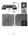
Figure 2 is an illustration of the use of a method of the invention for in situ fabricating nanopores in a transition metal dichalcogenide membrane in a molecular sensing system as described in Example 1. a: Schematic illustration of preparation of a freestanding MoS2 membrane ready for electrochemical formation of a nanopore. In the center of the supporting 20 nm thick SiNx membrane a single focused ion beam, focused ion beam (FIB) hole is drilled to suspend a small portion of an intact monolayer MoS2 flake. A single chip is mounted in the flow-cell for typical translocation experiments. A pair of electrodes (e.g. Ag/AgCl) is connected to a preamplifier is used to apply transmembrane voltage; b: Optical image of the SiNx membrane with a FIB drilled hole in the center. c: Optical image of the SiNx membrane with transferred triangular CVD-grown MoS2 monolayer; d: Low magnification TEM image of transferred CVD-grown MoS2 monolayer covering the FIB hole. The FIB hole is indicated by the black arrow; e: High resolution TEM of the lattice of MoS2 suspended over the FIB hole. The corresponding diffraction diagram is shown in the inset -
Figure 3 shows the leakage current characteristics of an intact membrane and during pore formation as described in Example 1 together with the visualization and modelization of the pore forming process. a: Leakage current-voltage (I-V) characteristic of an intact MoS2 membrane, for voltages below the critical voltage of 800 mV required for ECR which depends on the number of the membrane defects (more defects leads to higher current). c: Representative ionic current trace measured for a MoS2 membrane. Voltage is stepped by 100 mV with a 50 s holding, and the leakage current increases in accordance, being steady for a constant voltage. Sharp peaks at each voltage step originate from the capacitance charging. After a critical voltage, 800 mV is applied, the electrochemical reaction (ECR) starts (arrow), the current keeps increasing which triggers the feedback control to switch off voltage bias in order to halt the pore growth. c: Mechanism of ECR based MoS2 nanopore fabrication. A side view of the monolayer MoS2 lattice, emphasizing the lattice having single atom (S) vacancy or defect before ECR V<Vcritical (left), MoS2 lattice at V=Vcritical (nanopore starts to form, middle) and MoS2 lattice when nanopore (diameter d) is formed (right). d: Current-voltage (IV) characteristic of nanopores ranging in diameter from 1 to 20 nm - all nanopores are created via electrochemical reaction. Inset shows I-V characteristics for the system below and at the critical voltage. e: TEM images verify the nanopore formation and size (top being a zoom-in image of the bottom image). -
Figure 4 shows simulations of the electric potential distribution for the nanopore in two dimensions for a freshly formed pore having a diameter of 0.3 nm and comparison with a typical current trace of nanopore formation on graphene membrane. a: Electric potential distribution in the trans chamber in the immediate vicinity of the membrane surface and b: in the cis chamber. c: Electric potential distribution as a function of the distance from the pore. The applied potential was set to 800 mV and salt concentration was 1 M KCl. d: Typical current trace of nanopore formation on graphene membrane using ECR.A much higher transmembrane voltage, 2.8 V has to be applied to graphene to create a nanopore in graphene. -
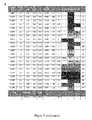
Figure 5 is schematization of nanopore forming in monolayer MoS2 starting from a monolayer MoS2 lattice a: Top view of the monolayer MoS2 lattice, the unit cell, u (parameter a=3.12 Å) is shown in grey ( Hulliger, & Lévy. Structural Chemistry of Layer-Type Phases, Springer, 1976). b: Ionic current-steplike features during the nanopore formation inFig. 2a . c: Custom Matlab code is used to detect steps in the raw ionic current trace (Raillon et al., 2012, Nanoscale, 4, 4916-4924 and histogram of the trace shown in b) with corresponding color coded atom groups cleaved in each step during the pore formation from 1 to 21. d: Illustrative schematic of polygon removal corresponding to the histogram trace. Aberration corrected TEM micrograph of suspended single layer MoS2 superimposed are the polygons which correspond to atom groups cleaved in thesteps Fig. 5c ) and corresponding area polygons shown in theFig. 5d starts fromstep 1 and goes up to step 21. e: The table represents the sequence of cleaving MoS2 unit cells and Mo and S atoms in 21 steps to form the pore. Istep is the distance between two adjacent peaks in the current histogram; D and A are effective pore diameter and pore area, respectively; N is the number of unit cells equivalent to the effective area; ΔA is the increments of A; ΔN is the increments of N; ΔX is the nearest integer or integer +1/3 or +2/3 of ΔN; the last column on the right stands for the number of unit cells. -
Figure 6 shows DNA translocation through a nanopore fabricated as described in Example 1. a: typical trace of pNEB plasmid DNA translocation through an electrochemically etchhed nanopore recorded at 450 mV. The trace is downsampled to 10 kHz for display. b: Scatter plot of events collected at 300 mV and 450 mV bias. Event detection is performed using OpenNanopore37 Matlab code. Expectedly, the increase in the bias voltage from 300 to 450 mV shortens the translocation time and enhances the current drop. -
Figure 7 shows selected events of λ-DNA translocation through a 4 nm ECR fabricated MoS2 nanopore by a method according to the invention as described in Example 1 and recorded in-situ right after pore formation at 200 mV as described in Example 2. Quantized levels in the ionic current represent the flexibility of λ-DNA when translocating through nanopore. -
Figure 8 shows and example of arrangement of setting for carrying out the process of the invention for the in situ formation of a nanopore on several devices comprising a 2D transition metal dichalcogenide membrane in parallel through the control of an integrated circuit configured for the monitoring of the application and cut-off (e.g. N- channel FPGA card) transmembrane voltages in parallel to each of the 2D transition metal dichalcogenide membranes. - Referring to the figures, in particular first to
Figures 1a and2 , a method for forming a nanopore in a transition metal dichalcogenide membrane, in a form of a thin layer (or a monolayer) 1 having from about 0.3 nm to 4 nm thickness (H m ) suspended in an electrically conductingliquid 2 comprises applying a transmembrane voltage (V) at a value higher than the oxidation potential of the transition metal of the said TMDC, measuring the ionic current (Ii) in the said electrically conducting liquid until the ionic current (Ii) has reached a value (I p ) corresponding to the electrical conductance of a pore within the metal dichalcogenide membrane having a prescribed diameter (D p ). - The TMDC
thin layer 1 is configured such that the portion of the TMDC thin layer where the formation of a nanopore will be carried out is suspended in an electrically conducting liquid and the other portion of the TMDC thin layer is supported by asupport layer 3. - The support layer can be of SiNx, glass, quartz, Al2O3, or HfO2 (or any other material that provides low capacitance membrane) with a support orifice of a diameter D s that allows the portion of the TDMC membrane where the pore formation should be conducted being suspended in the electrically conducting liquid.
- When the transmembrane voltage V is applied to the TMDC thin layer at a value higher than the oxidation potential of the transition metal of the said TMDC, TMDC start being oxidized through an ECR reaction and the formation of a
nanopore 4 is initiated. - The formation for a
nanopore 4 could be monitored through the measurement of an increase in the ionic current (Ii) in anelectrical circuit 5 formed between a voltage source V andelectrodes thin layer 1, and configured to measure the ionic current Ii by a current measurement circuit portion A. The current measurement circuit portion A measures the ionic current value which is representative of conductance through the pore in the TMDCthin layer 1 and therefore of the diameter Dp of thepore 4 formed in the TMDCthin layer 1. - Thin layers of MoS2 with good quality suitable for use in a device according to the invention can be prepared by both exfoliation and chemical vapor deposition (CVD) (Novoselov et al., PNAS, 2005, 102, 10541-1053 ; Liu et al. 2012, Nano Lett., 12, 1538-1544).
- Typically, the thickness of TDMC membranes according to the invention can be assessed by Raman /optical electron microscopy, photo-luminescence (PL) measurements and Atomic Force Microscopy (AFM).
- According to another particular aspect, the thickness of a TDMC membrane according to the invention may be less than 2 nm, typically from about 0.7 nm to less than 2 nm. In particular, the TDMC membrane is from about 0.7 nm (e.g. one layer) to about 1.4 nm thick (e.g. two layers).
- According to another aspect, pores in the TDMC membrane formed by a process of the invention are nanometer sized, typically from about 1 nm to 20 nm diameter (for example typically from about 1 nm to about 5 nm, for example less than 4 nm or less such as about 3 nm) and from about 0.3 nm to
- 1 nm thickness (for example about 0.7 nm). Typically, the size of the pores can be measured by Transmission electron microscopy (TEM) and calculated from the current -voltage characteristics.
- According to another aspect, the support layer can be a SiNx, glass, or quartz (or any other material that provides low capacitance membrane) with a support orifice that allows the portion of the TDMC membrane where the pore formation should be conducted being suspended in the electrically conducting liquid. According to a further aspect, the support orifice has typically a diameter of from about 20 nm to about 500 nm (e.g. 50 nm), like for example from about 200 nm to about 500 nm and from about 20 nm to 50 nm thick.
- According to a further aspect, the support layer can be coated with some curing layer such as polydimethylsiloxane (PDMS), while leaving the MoS2 nanopore exposed in order to reduce the dielectric noise. Alternatively, support layer can be a quartz, glass, or any other material that provides low capacitance membrane based support.
- According to a particular embodiment, the TDMC thin layer of the invention can be an active layer as described in
WO 2012/093360 . - According to a particular embodiment, the method of the invention can be carried out in a nanopore sensing device as generally described in
PCT/EP2015/053042 - Referring to
Figure 1b , is provided an illustration of a specific embodiment regarding steps of a method for forming a nanopore in a transition metal dichalcogenide membrane according to the invention: - (a) providing a TMDC thin layer mounted in a housing (e.g. polymethylmethacrylate (PMMA)) flow cell chamber on a support layer (e.g. SiNx) with a support orifice that allows the portion of the TDMC membrane where the pore formation will be conducted being suspended in the electrically conducting liquid, wherein the housing comprises a cis and a trans chamber and the TMDC thin layer is located at the interface of those two chambers;
- (b) filling cis and trans chambers with an aqueous solution (e.g. a mixture of ethanol/deionized water v/v, 1:1) for increasing its hydrophilicity (e.g. for about 15-35 min);
- (c) flushing the cis and trans chambers with an electrically conducting liquid (e.g. 1M KCl) such as the TMDC thin layer is immersed in said electrically conducting liquid;
- (d) immersing a pair of electrodes adapted to the electrically conducting liquid (e.g. freshly made Ag/AgCl electrodes) in the corresponding chambers and connected to a voltage source, for example through a programmed amplifier;
- (e) applying a transmembrane voltage by step-wise increments (e.g. 20-100 mV increments) and holding each step for about 25-50s;
- (f) measuring the ionic current (Ii) in the said electrically conducting liquid;
- (g) turning off the transmembrane voltage (i.e. by feed-back control) once the measured ionic current (Ii) has reached a value (I p ) corresponding to the electrical conductance of a pore in the TMDC thin layer having a prescribed diameter (d p ).
- (h) optionally replacing the electrically conducting liquid in the cis chamber with another electrically conducting liquid (e.g. suitable for nanopore biosensing).
- Apart from nanopore sensors, other applications for a method according to the invention can be envisioned such as water desalination devices such as described in Yuan & Gaoquan, 2014, Nanoporous graphene materials, Materials Today, 17 (2) 77-8 and Cohen-Tanugi Det al., 2012, 2012, Nano Letters, 12, p. 3602-3608.
- The invention having been described, the following examples are presented by way of illustration, and not limitation.
- The present example illustrates a method of the invention applied to the fabrication of individual nanopores on single-layer MoS2, with the electric field generated by Ag/AgCl electrodes located in two electrolytes compartments and positioned away from the membrane. As described below, the ECR process starts for a certain critical voltage applied to the membrane at a defect/vacancy present in the MoS2 membrane.
- Importantly, in the course of the ECR process, it is possible to control the successive removal of single or few MoS2 units from the monolayer MoS2 membranes. In this way, atom-by-atom nanopore engineering is achieved.
- A procedure for fabricating MoS2 nanopores using ECR is schematically illustrated in
Fig. 2a , where two chambers (cis and trans) are filled with aqueous buffer (1M KCl, pH 7.4) and biased by a pair of Ag/AgCl electrodes which are separated by a single-layer MoS2 membrane. Presence of an active site such as single-atom vacancy facilitates the removal of individual atoms and MoS2 unit cells from MoS2 lattice by ECR at voltages higher than the oxidation potential of MoS2 in aqueous media. This process is facilitated by the electric field focusing by the pore itself. To form freestanding membranes, CVD-grown monolayer MoS2 transferred from a sapphire substrate is suspended over focused ion beam (FIB) defined openings that ranged from 80 nm to 300 nm in diameter and were centered in a 20 nm thick SiNx membrane (Fig. 2b ). A typical optical image of the transferred triangular flake of CVD-grown monolayer MoS2 on the supporting silicon nitride membrane is shown inFig. 2c . The freestanding MoS2 membrane above the FIB defined opening can be further identified under TEM with low magnification (5 k×) as shown inFig. 2d . MoS2 flake is further characterized by Energy-dispersive X-ray spectroscopy (EDX) in TEM to reveal the chemical composition of the surface where elements of Mo and S are abundant in triangular areas. When moving to a high magnification (1 M ×) and focusing on the freestanding portion of MoS2 over the FIB opening, the atomic structure of MoS2 can be clearly resolved as shown inFig. 2e , and the diffractogram reflects the hexagonal symmetry of MoS2, as shown in the inset ofFig. 2e . - An intact MoS2 membrane is mounted into a custom made microfluidic flow-cell filled with an aqueous buffer and transmembrane potential is applied using a pair of Ag/AgCl electrodes as shown in
Fig. 2a . When a voltage is applied below the potential for electrochemical oxidation of the transition metal of the membrane, small leakage current is normally detected, typically on the order from tens to hundreds of picoamperes depending on the number of defects in the 2D membrane. As shown inFig. 3a , the leakage current displays a non-ohmic characteristic. To reach the critical voltage value for achieving an ECR, the potential is gradually stepped, as shown inFig. 3b . When the applied voltage is stepped up to 0.8 V (a critical voltage, indicated by the arrow), an increase of baseline current immediately occurs. This time-point indicates the nanopore creation which is associated to the electrochemical dissolution of MoS2 enhanced by the electrical potential focused on the active site as shown in the potential profile obtained by the finite element analysis simulation (Fig. 4a ). In other words, the pore growth continues at the initial, active site instead of another start on another defect because the pore itself focuses the applied electric potential and facilitates continuation of ECR on the active site where ECR process has already started. - In contrast to the avalanche-like dielectric breakdown process in silicon nitride, where a typically 10-minute waiting time for the filling of charge traps (Briggs et al., 2015, nanotechnology, 084004 , doi:10.1088/0957-4484/26/8/084004) under the application of critical voltage (> 10 V) is needed before breakdown occurs, electrochemical dissolution happens spontaneously at the critical voltage. In addition, the observed rise of ionic current shows a quite slow rate (∼ 0.4 nA/s). Therefore, it is possible to control the nanopore size by using an automatic feedback to cut off the voltage once the desired current/conductance threshold is reached. This feedback also helps to avoid multiple pore formation. Owing to the limited rates of electrochemical reaction, the MoS2 nanopore sculpting process is quite slow, occurring on time scales of dozens of seconds to several minutes.
Fig. 3e gives an example of ionic current trace to reach the threshold of 20 nA, for the critical voltage of 0.8 V. - Taking the advantage of existing theoretical insights to model the conductance-pore size relation (Kowalczyk et al., 2011, Nanotechnology, 22 , doi:Artn 315101 Doi 10.1088/0957-4484/22/31/315101), the conductance of the nanopore (G) can be described by

where σ, L and d are the ionic conductivity of solution, membrane thickness and nanopore diameter, respectively. Using this relation in combination with feedback on ECR that immediately stops the voltage once the desired pore conductance - that corresponds to a certain pore size - is reached, it is possible to fabricate pores ranging in diameter from 1-20 nm.Fig. 3e reveals current-voltage (I-V) characteristics of MoS2 nanopores fabricated by ECR with different estimated sizes ranging from 1 nm to 20 nm. The symmetric and linear I-V curves also imply the well-defined shape of the fabricated pores. Similarly, as shown in the inset of theFig. 3e , I-V characteristics across the membrane have been investigated in situ before and after ECR, confirming the pore formation. - To further verify the size of fabricated MoS2 nanopores, TEM has been used to image the newly formed nanopore. Exposure of 2D materials to electron radiation can induce large area damage and also open pores, as reported for both graphene (Fischbein et al., 2008, Applied Physics Letters, 93) and MoS2 (Liu et al., 2013, Nat. Commun., 4). Therefore, first aligned the beam was aligned on the suspended portion of MoS2 outside of the FIB opening and then quickly scanned the sample while taking care to minimally irradiate suspended MoS2 that houses ECR fabricated pore.
Fig, 2c shows a TEM image of an ECR-fabricated MoS2 nanopore. - For the sake of comparison, a few graphene membranes (prepared as described below) have also been tested by this method and higher voltages (2-3V) are required to fabricate pores as presented in Supporting Information, with the typical ionic current trace is displayed in
Fig. 4b . - The described ECR-based pore formation method benefits from the unique crystal structure of transition metal dichalcogenide (MX2) where atoms are situated in tree planes and linked by metal-chalcogenide bonds while in the case of graphene, carbon atoms are in the same plane and 3 bonds need to be removed to release one carbon atom. In addition, to remove carbon atoms, graphene needs to be oxidized to a higher valence state which presumably requires a higher voltage.
- The physics of the electrochemically fabricated nanopores is determined by the focused electrical field and surface chemistries. The electric field concentrates at surface irregularities or defects which can be considered as surface active sites, and focuses current flow at the site of the pore, and thus locally enhances the electrochemical dissolution, as shown in
Fig 3c . - The surface dissolution chemistries can be understood as a surface bound oxidation scheme with hole capture and electron injection to produce the MoS2 oxidation state (Bonde et al., 2008, Faraday Discussion 140, 219-231) as shown in

where MoS2 is oxidized into MoO3 which is water-soluble. Without being bound to any theory, this reaction is highly likely to happen considering the electrical potential (voltage bias) range applied to the membrane. Due to the current technical limitations of electron energy loss spectroscopy (EELS) analysis in the nanopore vicinity, it cannot be excluded the possibility that MoS2 is oxidized to other valence states. Once an active site is removed by the process described above, indicating the initial formation of the pore,Fig. 5a , the electric field, as simulated inFig. 4a , entirely focuses in this pore, which then prefers to enlarge the same pore since this is more energetically favorable than creating a second pore at another location. By applying at the beginning of the fabrication process a bias voltage higher than the critical voltage it might be possible to observe the formation of multiple pores. Given the stochastic nature of the pore creation process, with a configuration of voltage steps, multiple simultaneous nanoscale ECR events are highly unlikely. Furthermore, feedback control on the applied voltage to obtain the desirable conductance ensures the formation of a single nanopore. Finally, the formation of single nanopore is confirmed by TEM imaging. - The advantage of an ECR-based nanopore fabrication technique of the invention, apart from the benefit of being a fast and cheap production lies in the possibility of fine-tuning the diameter of nanopores with unprecedented, single-atom precision. The low nanopore enlarging speed is due to low voltages and the electrochemical dissolution nature of the process.
Fig. 5d is a 25-second long, continuous pore conductance trace that shows atomic precision during nanopore sculpting process. The trace starts from the critical point indicated inFig. 3b . Fitting to the conductance-nanopore size relation, it can be estimated a pore diameter growth rate of about 1 angstrom per second. After 25 seconds a pore with a diameter 1.9* nm (area of 2,9 nm2) has been formed. The area of such a pore is equivalent to almost exactly N = 34 unit cells of MoS2 where the area of the unit cell u = 0.0864 nm2 (Fig. 5a ). *The final pore size is 2,2, nm when one accounts for the initial 0.3 nm. - Surprisingly, the growth curve is not linear but step-like, as shown in
Fig. 5b . Necessarily, the effective size of the pore enlarges with the same step-like characteristic. These step-like features are commonly observed when working with voltages around 1V. To gain insights into these step-like features, the histogram of current values is plotted from this trace inFig. 5c , where 21 individual peaks can be extracted from the histogram. - The sequence of the pore size enlargement steps may be normalized by the unit cell area u and a sequence of MoS2 formula units and Mo and S atoms cleaved (corresponding to 21 current steps) to form the pore may be inferred, as presented in the
Fig. 5c and5e . Several snapshots of the pore formation process taken atsteps Fig. 5d . The area of polygons corresponding to the cleaved atom groups follows the honeycomb structure of single-layer MoS2, as presented in an aberration corrected TEM imageFig 5d and in the schematics shown inFig 5a . The observed atomic steps here reveal the ultimate precision (single atoms) that can be reached in engineering nanostructures with a process of nanopore forming of the invention. - The MoS2 membranes are prepared using the previously reported procedure (Liu et al., 2014, ) and as described below. Briefly, 20 nm thick supporting SiNx support membranes are manufactured using anisotropic KOH etching to obtain 10 µm × 10 µm to 50 µm × 50 µm membranes, with size depending on the size of the backside opening. Focused ion beam (FIB) is used to drill a 50-300 nm opening on that membrane. CVD-grown MoS2 flakes were transferred from sapphire substrates using MoS2 transfer stage in a manner similar to the widely used graphene transfer method and suspended on FIB opening (Dumcenco et al., 2014, arXiv preprint arXiv:1405.0129). Membranes are first imaged in the TEM with low magnification in order to check suspended MoS2 flakes on FIB opening.
- Monolayer MoS2 has been grown by chemical vapor deposition (CVD) on c-plane sapphire. After consecutive cleaning by acetone/isopropanol/DI-water the substrates were annealed for 1h at 1000 °C in air. After that, they were placed face-down above a crucible containing ∼5 mg MoO3 (≥ 99.998% Alfa Aesar) and loaded into a furnace with a 32 mm outer diameter quartz tube. CVD growth was performed at atmospheric pressure using ultrahigh-purity argon as the carrier gas. A second crucible containing 350 mg of sulfur (≥ 99.99% purity, Sigma Aldrich) was located upstream from the growth substrates. Further details of the procedure are described in Dumcenco et al., 2014, supra.
- Monolayer MoS2 grown on sapphire substrate (12 mm by 12 mm) is coated by A8 PMMA (495) and baked at 180 °C. A diamond scriber was used to cut it into 4 pieces. Each piece is immersed into 30%w KOH at 85-90°C for the detachment. Capillary force might be used in the interface between polymer and sapphire to facilitate the detachment and reduce the etching time in the KOH. The detached polymer film was repeatedly in DI water. Lastly, the "fishing" method of graphene transfer can be used to transfer CVD MoS2 to the target SiNx membrane.
- For the nanopore fabrication experiments, after mounting in the polymethylmethacrylate (PMMA) chamber (
Figure 1b , step (a)), the chips were wetted with H2O:ethanol (v:v, 1:1) for at least 20 min (Figure 1b , step (b)). 1 M KCl solution buffered with 10 mM Tris-HCl and 1 mM EDTA at pH 8.0 was injected in the chamber (Figure 1b , step (c)). A pair of chlorinated Ag/AgCl electrodes was immersed in the chamber (Figure 1b , step (d)) and employed to apply the transmembrane voltage and the current between the two electrodes was measured by a FEMTO DLPCA-200 amplifier (FEMTO® Messtechnik GmbH). A low voltage (100 mV) was applied to check the current leakage of the membrane. If the leakage current was below 1 nA, the voltage bias was set up in 100 mV steps (25 s for each step) (Figure 1b , step (e)). At a critical voltage (i.e. 800 mV), the current started to immediately increase above the leakage level. A FPGA card and custom-made LabView software was used for applying the voltage and monitoring the conductance (Figure 1b , step (f)). The critical voltage was automatically shut-down by a feedback control implemented in LabView program as soon as the desirable conductance was reached (Figure 1b , step (g)). Nanopores were further imaged using a JEOL 2200FS high-resolution transmission electron microscope (HRTEM). STEM-EDX was performed on a ChemiSTEM-equipped FEI Tecnai Osiris transmission electron microscope (TEM). Aberration corrected TEM micrographs were taken on FEI Titan Themis. - Large-area graphene films are grown on copper foils. The growth takes place under the flow of a methane / argon / hydrogen reaction gas mixture at a temperature of 1'000°C. At the end of the growth, the temperature is rapidly decreased and the gas flow turned off. The copper foils are then coated by PMMA and the copper etched away, resulting in a cm-scale graphene film ready to be transferred on the chips with membranes for fabricating nanopores with a method of the invention.
- To estimate the potential drop in a defect in a MoS2 membrane a finite element analysis was performed using COMSOL Multiphysics 4.4b. A coupled set of the Poisson-Nernst-Planck equations was solved in a 3D geometry with axial symmetry. In the modeled configuration cis and trans chambers were connected by a 0.3 nm pore in a 0.7 nm thick membrane suspended on a 50 nm wide and 20 nm thick hole. A 0.3 nm diameter defect can correspond to the absence of a unit cell of MoS2. In the model, the applied potential was set to 800 mV and salt concentration was 1 M KCl. The minimal mesh size used was less than 0.2 Å.
- All analysis were implemented in Matlab R2014b. The raw signal was down-sampled to 5 kHz and then filtered using the edge-preserving Chung-Kennedy (CK) filter ( Chung et al., 1991, J. Neurosci. Methods, 40, 71-86 ). The pore formation in 21 steps, presented on
Fig. 5 can be as follows: the growth of the nanopore is due to sequential cleaving of unit cells from MoS2 lattice. The final pore area is 2.9 nm2, which corresponds to 34 unit cells. Increments in the effective pore size ΔA are normalized by unit cell size u = 0.0864 nm2. The obtained number ΔN =ΔA/u was rounded to the nearest integer, integer +1/3 or integer +2/3 to get ΔX, the number of MoS2 unit cells cleaved during the pore formation process. It is assumed that 1/3 corresponds to a S2 group and 2/3 to a Mo atom, corresponding to the partial cleaving of a unit cell. It should be noted that the two S atoms in MoS2 are stacked vertically and their combined surface area is smaller than that for Mo (which has about 50% larger radius). - The sequence of cleaving MoS2 unit cells and Mo and S atoms in 21 steps to form the pore is given in the table from
Fig. 5e . In order to depict the sequence of the pore formation, the numbering of the lines in this table and polygons based on HRTEM image starts from 1 to 21. Lifetime of the steps in the sequence is given in the same table. Initially irregular pore gradually becomes more symmetrical. The atom groups have been selected in the manner to minimize the number of dangling bonds at the edge of the pore. The pore formation sequence is not unique, however, the dangling bond constraint significantly reduces the number of pore formation scenarios and induces more symmetrical pore shape. - To test the performance of ECR-fabricated pores, DNA translocation experiments were carried and detected the translocation events by the current drops below the baseline current. ECR fabricated MoS2 nanopores consistently produces low-1/f noise on the current baseline in the range of 50-100 pA. The major contribution to the 1/f noise in 2D membrane nanopores can be attributed to mechanical fluctuations of the thin membranes. Higher frequency fluctuations are produced by the method itself. Fluctuation noise can be significantly reduced by using a smaller supporting opening, or operating at low temperatures. To show the ability of ECR fabricated nanopore for DNA detection, 2.7 kbp pNEB plasmid DNA (New England Biolabs) is translocated through a relatively large MoS2 nanopore (25 nm) to eliminate the pore-DNA interaction and multiple conformation issues.
Fig. 6a displays only one-level events indicating an extended (unfolded) DNA conformation, with SNR >10. Scatter plots are used to describe the statistics of DNA translocation as shown inFig. 6b . The signal amplitude also increases linearly with the applied voltage, which is 0.5 nA for 450 mV and 0.38 nA for 300 mV as shown in the histogramFig. 6b . Dwell times are also comparable with DNA translocation through a TEM-drilled MoS2 nanopore of a similar diameter, for the same DNA and under same bias conditions. In addition, λ-DNA (48 k bp) is also translocated through an ECR-fabricated nanopore. As expected, folding scenario can be observed, manifested by quantization of current levels guided by dash lines. The upper dash line is the one level conductance, indicating a linear translocation. The bottom dash line is the two level conductance, indicating a folded translocation (Fig. 7 ). - Current-voltage (I-V) characteristic and DNA translocation were recorded on an Axopatch 200B patch clamp amplifier (Molecular Devices, Inc. Sunnyvale, CA). DNA samples (pNEB193, plasmid 2.7 k bp, New England; λ-DNA, 48 k bp, New England) were diluted by mixing 10 µL of λ-DNA or pNEB stock solution with 490
µL 1 M KCl buffer. NI PXI-4461 card was used for data digitalization and custom-made LabView software for data acquisition using Axopatch 200B. The sampling rate is 100 kHz and a built-in low-pass filter at 10 kHz is used. Data analysis enabling event detection is performed offline using a custom open source Matlab code, named OpenNanopore (Raillon et al, Nanoscale, 2012, 4, 4916-4924) (http://lben.epfl.ch/page-79460-en.html). - Altogether, those data support that a method of the invention leads to reproducible and fully characterized nanopores by I-V characteristics and size as confirmed by TEM. Further, the intrinsic electrochemical reaction kinetics permits an advantageously high precision for nanopore fabrication at the atom level which can be monitored by the observed step-like features in the ionic current traces. Finally, the nanopores obtained through a method of the invention have demonstrated to allow DNA translocation and their sensing as fully functional nanopores.
Claims (15)
- A method for forming a nanopore in a membrane of transition metal dichalcogenide (TMDC) crystals comprising the steps of:- providing at least one TMDC thin layer having from about 0.3 nm to 5 nm thickness (H m ) suspended in an electrically conducting liquid ;- applying a transmembrane voltage (V) at a value slightly higher than the oxidation potential of the transition metal of the said at least one TMDC thin layer configured for an electrochemical atomic etching of said transition metal dichalcogenide thin layer;- measuring the ionic current (Ii) in the said electrically conducting liquid;- turning off the transmembrane voltage once the ionic current (Ii) has reached a value (I p ) corresponding to the electrical conductance of a pore within the said TMDC thin layer having a prescribed diameter (d p ).
- A method according to claim 1 wherein the TMDC is of chemical formula is MX2, where M is a transition metal atom and X is a chalcogen (S, Se, or Te).
- A method according to claim 1 the TMDC is selected from MoS2, SnSe2, WS2, TeS2, MoSe2, WSe2, and TeSe2.
- A method according to any one of claims 1 to 3, wherein TMDC thin layer is a single or double layer.
- A method according to any one of claims 1 to 4, wherein the TMDC layer comprises MoS2 thin layers or is a MoS2 monolayer.
- A method according to claim 5 wherein the applied transmembrane voltage is from about 800 mV to about 1'000 mV.
- A method according to any one of claims 1 to 6, wherein the transmembrane voltage is applied in an essentially constant DC manner.
- A method according to any one of claims 1 to 7, wherein the ionic current is measured in an ionic current circuit comprising a pair of electrodes, for instance Ag/AgCl electrodes, one of the pair of electrodes located in the electrically conducting liquid on one side of the membrane and the other of the pair of electrodes located in the electrically conducting liquid on the other side of the membrane.
- A method according to any one of claims 1 to 8, wherein the electrically conducting liquid comprises or consists in an aqueous liquid comprising an electrolyte.
- A method according to any one of claims 1 to 9, wherein the TMDC thin layer is a sensing membrane already integrated in a biosensing device.
- A method according to any one claims 1 to 10 wherein the size of the pore is from about 1 nm to about 5 nm.
- A method according to any one claims 1 to 11, wherein the electrically conducting liquid is an aqueous ionic solution selected from water and KC1 or any inorganic salts such as LiCl, NaCl, MgCl2 CaCl2.
- A method according to any one of claims 1 to 12, wherein the turning off of the transmembrane voltage is achieved by an automatic switch which is activated through a feed-back control circuit when said prescribed electrical conductance current is reached.
- A method according to any one of claims 1 to 13, wherein more than one TMDC thin layers are provided and a transmembrane voltage is applied to each of the TMDC thin layers in parallel.
- A method according for manufacturing a biosensing nanopore device comprising a step of forming a nanopore according to any one of claims 1 to 14.
Priority Applications (8)
| Application Number | Priority Date | Filing Date | Title |
|---|---|---|---|
| EP15158894.4A EP3067693A1 (en) | 2015-03-12 | 2015-03-12 | Nanopore forming method and uses thereof |
| PCT/IB2016/051425 WO2016142925A1 (en) | 2015-03-12 | 2016-03-12 | Nanopore forming method and uses thereof |
| EP16715097.8A EP3268736B1 (en) | 2015-03-12 | 2016-03-12 | Nanopore forming method and uses thereof |
| US15/688,264 US10364507B2 (en) | 2015-03-12 | 2017-08-28 | Nanopore forming method and uses thereof |
| US16/432,163 US10947637B2 (en) | 2015-03-12 | 2019-06-05 | Nanopore forming method and uses thereof |
| US17/174,230 US11401625B2 (en) | 2015-03-12 | 2021-02-11 | Nanopore forming method and uses thereof |
| US17/876,161 US11753738B2 (en) | 2015-03-12 | 2022-07-28 | Nanopore forming method and uses thereof |
| US18/230,398 US20230374693A1 (en) | 2015-03-12 | 2023-08-04 | Nanopore forming method and uses thereof |
Applications Claiming Priority (1)
| Application Number | Priority Date | Filing Date | Title |
|---|---|---|---|
| EP15158894.4A EP3067693A1 (en) | 2015-03-12 | 2015-03-12 | Nanopore forming method and uses thereof |
Publications (1)
| Publication Number | Publication Date |
|---|---|
| EP3067693A1 true EP3067693A1 (en) | 2016-09-14 |
Family
ID=52648930
Family Applications (1)
| Application Number | Title | Priority Date | Filing Date |
|---|---|---|---|
| EP15158894.4A Withdrawn EP3067693A1 (en) | 2015-03-12 | 2015-03-12 | Nanopore forming method and uses thereof |
Country Status (1)
| Country | Link |
|---|---|
| EP (1) | EP3067693A1 (en) |
Citations (3)
| Publication number | Priority date | Publication date | Assignee | Title |
|---|---|---|---|---|
| WO2012093360A1 (en) | 2011-01-04 | 2012-07-12 | Ecole Polytechnique Federale De Lausanne (Epfl) | Semiconductor device |
| WO2013167952A1 (en) | 2012-05-07 | 2013-11-14 | The University Of Ottawa | Method for controlling the size of solid-state nanopores |
| WO2014144818A2 (en) | 2013-03-15 | 2014-09-18 | President And Fellows Of Harvard College | Fabrication of nanopores in atomically-thin membranes by ultra-short electrical pulsing |
-
2015
- 2015-03-12 EP EP15158894.4A patent/EP3067693A1/en not_active Withdrawn
Patent Citations (3)
| Publication number | Priority date | Publication date | Assignee | Title |
|---|---|---|---|---|
| WO2012093360A1 (en) | 2011-01-04 | 2012-07-12 | Ecole Polytechnique Federale De Lausanne (Epfl) | Semiconductor device |
| WO2013167952A1 (en) | 2012-05-07 | 2013-11-14 | The University Of Ottawa | Method for controlling the size of solid-state nanopores |
| WO2014144818A2 (en) | 2013-03-15 | 2014-09-18 | President And Fellows Of Harvard College | Fabrication of nanopores in atomically-thin membranes by ultra-short electrical pulsing |
Non-Patent Citations (20)
| Title |
|---|
| BONDE ET AL., FARADAY DISCUSSIONS, vol. 140, 2008, pages 219 - 231 |
| BRANTON ET AL., NATURE BIOTECHNOLOGY, vol. 26, 2008, pages 1146 |
| BRIGGS ET AL., NANOTECHNOLOGY, 2015, pages 084004 |
| CHUNG ET AL., J. NEUROSCI. METHODS, vol. 40, 1991, pages 71 - 86 |
| COHEN-TANUGI D ET AL., NANO LETTERS, vol. 12, 2012, pages 3602 - 3608 |
| DEKKER, NATURE NANOTECHNOLOGY, vol. 2, 2007, pages 209 |
| FISCHBEIN ET AL., APPLIED PHYSICS LETTERS, 2008, pages 93 |
| GARAJ ET AL., NATURE, vol. 467, 2010, pages 190 |
| HULLIGER; LEVY: "Structural Chemistry of Layer-Type Phases", 1976, SPRINGER |
| ITARU YANAGI ET AL: "Fabricating nanopores with diameters of sub-1 nm to 3 nm using multilevel pulse-voltage injection", SCIENTIFIC REPORTS, vol. 4, 21 May 2014 (2014-05-21), XP055200768, DOI: 10.1038/srep05000 * |
| KOWALCZYK ET AL., NANOTECHNOLOGY, 2011, pages 22 |
| KWOK ET AL., PLOS ONE, vol. 9, 2014 |
| LIU ET AL., ACS NANO, vol. 8, 2014, pages 2504 - 2511 |
| LIU ET AL., NANO LETT., vol. 12, 2012, pages 1538 - 1544 |
| LIU ET AL., NAT. COMMUN., 2013, pages 4 |
| NOVOSELOV ET AL., PNAS, vol. 102, 2005, pages 10541 - 1053 |
| PARK ET AL., SMALL, vol. 3, 2007, pages 116 - 119 |
| RAILLON ET AL., NANOSCALE, vol. 4, 2012, pages 4916 - 4924 |
| SIWY ET AL., PHYSICAL REVIEW LETTERS, vol. 89, 2002, pages 198103 |
| YUAN; GAOQUAN: "Nanoporous graphene materials", MATERIALS TODAY, vol. 17, no. 2, 2014, pages 77 - 8 |
Similar Documents
| Publication | Publication Date | Title |
|---|---|---|
| US11753738B2 (en) | Nanopore forming method and uses thereof | |
| Chou et al. | Lifetime and stability of silicon nitride nanopores and nanopore arrays for ionic measurements | |
| Nioradze et al. | Organic contamination of highly oriented pyrolytic graphite as studied by scanning electrochemical microscopy | |
| DE112007001084B4 (en) | Nanopore membrane and process for its preparation and its surface modification | |
| Thiruraman et al. | Stochastic ionic transport in single atomic zero-dimensional pores | |
| US7824620B2 (en) | Nano- and micro-scale structures: methods, devices and applications thereof | |
| Bentley et al. | High-resolution ion-flux imaging of proton transport through graphene| nafion membranes | |
| KR102065745B1 (en) | Method for contrilling the size of solid-state nanopores | |
| Kang et al. | Multiscale analysis of electrocatalytic particle activities: linking nanoscale measurements and ensemble behavior | |
| Bhardwaj et al. | Fabrication of angstrom-scale two-dimensional channels for mass transport | |
| Kim et al. | The fabrication of integrated carbon pipes with sub-micron diameters | |
| Han et al. | Bottom-up synthesis of ordered metal/oxide/metal nanodots on substrates for nanoscale resistive switching memory | |
| Wang et al. | Voltammetric mapping of hydrogen evolution reaction on Pt locally via scanning electrochemical cell microscopy | |
| Ankah et al. | The influence of halides on the initial selective dissolution of Cu3Au (1 1 1) | |
| Toleukhanova et al. | Graphene electrode for studying CO2 electroreduction nanocatalysts under realistic conditions in microcells | |
| EP2908128A1 (en) | Molecular sensing device | |
| Li et al. | Evaluating graphene and molybdenum disulfide nanopores for DNA sequencing | |
| EP4454740A1 (en) | Nature-inspired stalactite nanostructures such as nanopores for biosensing and energy harvesting | |
| Briggs et al. | Fabricating Solid-State Nanopores for Single-Molecule Sensing | |
| Das | Nanostructure Engineering in Two-Dimensional Materials Beyond Graphene | |
| Alarcon et al. | Dynamic Perturbation of the Electrical Double Layer with an Electrochemical AFM for Confined Metal Electrodeposition | |
| Masih Das | Nanostructure Engineering In Two-Dimensional Materials Beyond Graphene | |
| Bhardwaj | Development of Facile Nanofabrication Technique of 2D Materials Membrane for Electrocatalysis and Molecular Transport | |
| Bellunato | Unconventional fabrication of 2D nanostructures and graphene edges | |
| Wahab | Single entity electrochemical imaging of materials for green energy |
Legal Events
| Date | Code | Title | Description |
|---|---|---|---|
| PUAI | Public reference made under article 153(3) epc to a published international application that has entered the european phase |
Free format text: ORIGINAL CODE: 0009012 |
|
| AK | Designated contracting states |
Kind code of ref document: A1 Designated state(s): AL AT BE BG CH CY CZ DE DK EE ES FI FR GB GR HR HU IE IS IT LI LT LU LV MC MK MT NL NO PL PT RO RS SE SI SK SM TR |
|
| AX | Request for extension of the european patent |
Extension state: BA ME |
|
| STAA | Information on the status of an ep patent application or granted ep patent |
Free format text: STATUS: THE APPLICATION IS DEEMED TO BE WITHDRAWN |
|
| 18D | Application deemed to be withdrawn |
Effective date: 20170315 |