EP3065416A1 - Semiconductor integrated device for acoustic applications with contamination protection element, and manufacturing method thereof - Google Patents
Semiconductor integrated device for acoustic applications with contamination protection element, and manufacturing method thereof Download PDFInfo
- Publication number
- EP3065416A1 EP3065416A1 EP15200515.3A EP15200515A EP3065416A1 EP 3065416 A1 EP3065416 A1 EP 3065416A1 EP 15200515 A EP15200515 A EP 15200515A EP 3065416 A1 EP3065416 A1 EP 3065416A1
- Authority
- EP
- European Patent Office
- Prior art keywords
- acoustic
- filtering
- access opening
- openings
- filtering module
- Prior art date
- Legal status (The legal status is an assumption and is not a legal conclusion. Google has not performed a legal analysis and makes no representation as to the accuracy of the status listed.)
- Withdrawn
Links
Images



Classifications
-
- H—ELECTRICITY
- H04—ELECTRIC COMMUNICATION TECHNIQUE
- H04R—LOUDSPEAKERS, MICROPHONES, GRAMOPHONE PICK-UPS OR LIKE ACOUSTIC ELECTROMECHANICAL TRANSDUCERS; ELECTRIC HEARING AIDS; PUBLIC ADDRESS SYSTEMS
- H04R1/00—Details of transducers, loudspeakers or microphones
- H04R1/08—Mouthpieces; Microphones; Attachments therefor
- H04R1/083—Special constructions of mouthpieces
- H04R1/086—Protective screens, e.g. all weather or wind screens
-
- B—PERFORMING OPERATIONS; TRANSPORTING
- B81—MICROSTRUCTURAL TECHNOLOGY
- B81B—MICROSTRUCTURAL DEVICES OR SYSTEMS, e.g. MICROMECHANICAL DEVICES
- B81B7/00—Microstructural systems ; Auxiliary parts of microstructural devices or systems
- B81B7/0032—Packages or encapsulation
- B81B7/0058—Packages or encapsulation for protecting against damages due to external chemical or mechanical influences, e.g. shocks or vibrations
-
- B—PERFORMING OPERATIONS; TRANSPORTING
- B81—MICROSTRUCTURAL TECHNOLOGY
- B81B—MICROSTRUCTURAL DEVICES OR SYSTEMS, e.g. MICROMECHANICAL DEVICES
- B81B7/00—Microstructural systems ; Auxiliary parts of microstructural devices or systems
- B81B7/0032—Packages or encapsulation
- B81B7/0061—Packages or encapsulation suitable for fluid transfer from the MEMS out of the package or vice versa, e.g. transfer of liquid, gas, sound
-
- B—PERFORMING OPERATIONS; TRANSPORTING
- B81—MICROSTRUCTURAL TECHNOLOGY
- B81C—PROCESSES OR APPARATUS SPECIALLY ADAPTED FOR THE MANUFACTURE OR TREATMENT OF MICROSTRUCTURAL DEVICES OR SYSTEMS
- B81C1/00—Manufacture or treatment of devices or systems in or on a substrate
- B81C1/00015—Manufacture or treatment of devices or systems in or on a substrate for manufacturing microsystems
- B81C1/00261—Processes for packaging MEMS devices
- B81C1/00309—Processes for packaging MEMS devices suitable for fluid transfer from the MEMS out of the package or vice versa, e.g. transfer of liquid, gas, sound
-
- H—ELECTRICITY
- H04—ELECTRIC COMMUNICATION TECHNIQUE
- H04R—LOUDSPEAKERS, MICROPHONES, GRAMOPHONE PICK-UPS OR LIKE ACOUSTIC ELECTROMECHANICAL TRANSDUCERS; ELECTRIC HEARING AIDS; PUBLIC ADDRESS SYSTEMS
- H04R19/00—Electrostatic transducers
- H04R19/005—Electrostatic transducers using semiconductor materials
-
- H—ELECTRICITY
- H04—ELECTRIC COMMUNICATION TECHNIQUE
- H04R—LOUDSPEAKERS, MICROPHONES, GRAMOPHONE PICK-UPS OR LIKE ACOUSTIC ELECTROMECHANICAL TRANSDUCERS; ELECTRIC HEARING AIDS; PUBLIC ADDRESS SYSTEMS
- H04R19/00—Electrostatic transducers
- H04R19/04—Microphones
-
- H—ELECTRICITY
- H04—ELECTRIC COMMUNICATION TECHNIQUE
- H04R—LOUDSPEAKERS, MICROPHONES, GRAMOPHONE PICK-UPS OR LIKE ACOUSTIC ELECTROMECHANICAL TRANSDUCERS; ELECTRIC HEARING AIDS; PUBLIC ADDRESS SYSTEMS
- H04R31/00—Apparatus or processes specially adapted for the manufacture of transducers or diaphragms therefor
-
- H—ELECTRICITY
- H04—ELECTRIC COMMUNICATION TECHNIQUE
- H04R—LOUDSPEAKERS, MICROPHONES, GRAMOPHONE PICK-UPS OR LIKE ACOUSTIC ELECTROMECHANICAL TRANSDUCERS; ELECTRIC HEARING AIDS; PUBLIC ADDRESS SYSTEMS
- H04R31/00—Apparatus or processes specially adapted for the manufacture of transducers or diaphragms therefor
- H04R31/006—Interconnection of transducer parts
-
- B—PERFORMING OPERATIONS; TRANSPORTING
- B81—MICROSTRUCTURAL TECHNOLOGY
- B81B—MICROSTRUCTURAL DEVICES OR SYSTEMS, e.g. MICROMECHANICAL DEVICES
- B81B2201/00—Specific applications of microelectromechanical systems
- B81B2201/02—Sensors
- B81B2201/0257—Microphones or microspeakers
-
- B—PERFORMING OPERATIONS; TRANSPORTING
- B81—MICROSTRUCTURAL TECHNOLOGY
- B81B—MICROSTRUCTURAL DEVICES OR SYSTEMS, e.g. MICROMECHANICAL DEVICES
- B81B2203/00—Basic microelectromechanical structures
- B81B2203/01—Suspended structures, i.e. structures allowing a movement
- B81B2203/0127—Diaphragms, i.e. structures separating two media that can control the passage from one medium to another; Membranes, i.e. diaphragms with filtering function
-
- B—PERFORMING OPERATIONS; TRANSPORTING
- B81—MICROSTRUCTURAL TECHNOLOGY
- B81B—MICROSTRUCTURAL DEVICES OR SYSTEMS, e.g. MICROMECHANICAL DEVICES
- B81B2207/00—Microstructural systems or auxiliary parts thereof
- B81B2207/01—Microstructural systems or auxiliary parts thereof comprising a micromechanical device connected to control or processing electronics, i.e. Smart-MEMS
- B81B2207/012—Microstructural systems or auxiliary parts thereof comprising a micromechanical device connected to control or processing electronics, i.e. Smart-MEMS the micromechanical device and the control or processing electronics being separate parts in the same package
-
- B—PERFORMING OPERATIONS; TRANSPORTING
- B81—MICROSTRUCTURAL TECHNOLOGY
- B81B—MICROSTRUCTURAL DEVICES OR SYSTEMS, e.g. MICROMECHANICAL DEVICES
- B81B2207/00—Microstructural systems or auxiliary parts thereof
- B81B2207/07—Interconnects
-
- B—PERFORMING OPERATIONS; TRANSPORTING
- B81—MICROSTRUCTURAL TECHNOLOGY
- B81C—PROCESSES OR APPARATUS SPECIALLY ADAPTED FOR THE MANUFACTURE OR TREATMENT OF MICROSTRUCTURAL DEVICES OR SYSTEMS
- B81C2203/00—Forming microstructural systems
- B81C2203/07—Integrating an electronic processing unit with a micromechanical structure
- B81C2203/0785—Transfer and j oin technology, i.e. forming the electronic processing unit and the micromechanical structure on separate substrates and joining the substrates
-
- H—ELECTRICITY
- H04—ELECTRIC COMMUNICATION TECHNIQUE
- H04R—LOUDSPEAKERS, MICROPHONES, GRAMOPHONE PICK-UPS OR LIKE ACOUSTIC ELECTROMECHANICAL TRANSDUCERS; ELECTRIC HEARING AIDS; PUBLIC ADDRESS SYSTEMS
- H04R2201/00—Details of transducers, loudspeakers or microphones covered by H04R1/00 but not provided for in any of its subgroups
- H04R2201/003—Mems transducers or their use
-
- H—ELECTRICITY
- H10—SEMICONDUCTOR DEVICES; ELECTRIC SOLID-STATE DEVICES NOT OTHERWISE PROVIDED FOR
- H10W—GENERIC PACKAGES, INTERCONNECTIONS, CONNECTORS OR OTHER CONSTRUCTIONAL DETAILS OF DEVICES COVERED BY CLASS H10
- H10W90/00—Package configurations
- H10W90/701—Package configurations characterised by the relative positions of pads or connectors relative to package parts
- H10W90/751—Package configurations characterised by the relative positions of pads or connectors relative to package parts of bond wires
- H10W90/753—Package configurations characterised by the relative positions of pads or connectors relative to package parts of bond wires between laterally-adjacent chips
-
- H—ELECTRICITY
- H10—SEMICONDUCTOR DEVICES; ELECTRIC SOLID-STATE DEVICES NOT OTHERWISE PROVIDED FOR
- H10W—GENERIC PACKAGES, INTERCONNECTIONS, CONNECTORS OR OTHER CONSTRUCTIONAL DETAILS OF DEVICES COVERED BY CLASS H10
- H10W90/00—Package configurations
- H10W90/701—Package configurations characterised by the relative positions of pads or connectors relative to package parts
- H10W90/751—Package configurations characterised by the relative positions of pads or connectors relative to package parts of bond wires
- H10W90/754—Package configurations characterised by the relative positions of pads or connectors relative to package parts of bond wires between a chip and a stacked insulating package substrate, interposer or RDL
Definitions
- the present invention relates to a semiconductor integrated device, for acoustic applications, with a contamination protection element, and to the manufacturing method thereof.
- the semiconductor integrated device includes a MEMS acoustic transducer
- the contamination protection element is a filter adapted to protect the MEMS acoustic transducer from dust.
- an acoustic transducer in particular a microphone of the MEMS (Micro-Electro-Mechanical System) type comprises a membrane sensitive structure designed to transduce acoustic-pressure waves into an electrical quantity (for example, a capacitive variation), and a reading electronics designed to carry out appropriate processing operations (amongst which amplification and filtering operations) on said electrical quantity for supplying an electrical output signal (for example, a voltage) representing the acoustic-pressure wave received.
- MEMS Micro-Electro-Mechanical System
- the microelectromechanical sensitive structure in general comprises a mobile electrode, obtained as diaphragm or membrane, set facing a fixed electrode, for providing the plates of a variable-capacitance detection capacitor.
- the mobile electrode is anchored by a first, generally perimetral, portion thereof to a structural layer, whereas a second portion thereof, which is generally central, is free to move or bend in response to the pressure exerted by the incident acoustic-pressure waves.
- the mobile electrode and the fixed electrode thus provide a capacitor, and bending of the membrane that constitutes the mobile electrode causes a variation of capacitance, as a function of the acoustic signal to be detected.
- the acoustic-transducer device 19 comprises a first die 21 that integrates a MEMS structure 1 provided with a membrane 2, mobile and of conductive material, which faces a rigid plate 3 (whereby is meant an element that is relatively rigid with respect to the membrane 2, which is, instead, flexible).
- the rigid plate 3 includes at least one conductive layer facing the membrane 2 so that the membrane 2 and the rigid plate 3 form facing plates of a capacitor.
- the membrane 2 which in use undergoes deformation in response to incident acoustic-pressure waves, is at least partially suspended over a structural layer 5 and directly faces a cavity 6, obtained by forming a trench in a rear surface 5b of the structural layer 5 (the rear portion 5b is opposite to a front surface 5a of the same structural layer 5, set in the proximity of the membrane 2).
- the MEMS structure 1 is housed in an internal cavity 8 of a package 20, together with a further die 22, of semiconductor material, which integrates a processing circuit, or ASIC (Application-Specific Integrated Circuit) 22'.
- the ASIC 22' is electrically coupled to the MEMS structure 1 by an electrical conductor 25', which connects respective pads 26' of the first and second dice 21, 22.
- the first and second dice 21, 22 are coupled side by side on a substrate 23 of the package 20.
- the first die 21 is coupled to the substrate 23 at the rear surface 5b of the structural layer 5, for example by an adhesive layer.
- the second die 22 is coupled to the substrate 23 at a rear surface 22b thereof.
- the ASIC 22' is provided on a front surface 22a of the second die 22, opposite to the rear surface 22b.
- Appropriate metallization layers and vias are provided in the substrate 23 for routing the electrical signals onto the outside of the package 20. Further electrical connections 25", obtained with the wire-bonding technique, are provided between pads 26" of the second die 22 and respective pads 26" of the substrate 23.
- Said covering 27 may be of metal or pre-moulded plastic.
- Electrical-connection elements 29 for example in the form of conductive lands, are provided at the underside of the substrate 23 (the side exposed outwards), for soldering and electrical connection to a printed-circuit board.
- the substrate 23 further has a through opening, or hole, 28, which sets in fluid communication the cavity 6 of the first die 21 with the environment external to the package 20.
- the through opening 28 (in what follows referred to as "sound port") enables introduction of a flow of air from outside the package 20 and of the acoustic-pressure waves, which, impinging upon the membrane 2, deflect it.
- the sensitivity of the acoustic transducer depends upon the mechanical characteristics of the membrane 2 of the MEMS structure 1, and further upon the assembly of the membrane 2 and of the rigid plate 3. Further, the volume of the acoustic chamber formed by the cavity 6 directly affects the acoustic performance, determining the resonance frequency of the acoustic transducer.
- a filter illustrated only schematically in Figure 1 , and designated by the reference 30 outside the package 20 and facing the sound port 28 (at a distance therefrom).
- This filter 30 is, for example, coupled to a protective shell of a portable device (e.g., a cellphone) that houses the package 20.
- the package 20 is housed inside the protective shell of the portable device itself in such a way that the sound port 28 in turn faces a respective through opening, or hole, made through the protective shell of the portable device by interposition of the filter 30 itself.
- the filters currently used are mounted manually on the protective shell of the portable device and consequently present excessive dimensions with respect to the actual operating need, which is to protect exclusively the cavity 6, in addition, obviously, to the membrane 2 and the rigid plate 3.
- the filter 30 prevents entry of contaminating particles through the hole made through the protective shell of the portable device, but does not solve the problem of contamination deriving from particles of dust or other debris coming from various sources (for example, on account of a not perfectly hermetic closing of the protective shell).
- filters of the known type are altogether ineffective in regard to protection from contaminating agents during intermediate manufacturing and assembly steps, i.e., during steps of assembly of the package in the portable device.
- the aim of the present invention is to provide a solution to the problems illustrated previously.
- FIG. 2 shows, in cross-sectional view, an acoustic-transducer device 51 according to one aspect of the present disclosure. Elements that are common to the acoustic-transducer device 51 of Figure 2 and to the acoustic-transducer device 19 of Figure 1 are designated by the same reference numbers and are not described any further.
- the acoustic-transducer device 51 of Figure 2 includes a package 50, formed by the base substrate 23 and by the covering element 27.
- the latter has a substantially cup-shaped conformation and is coupled to the base substrate 23 to form the cavity, or internal space, 8 of the package 50.
- Made throughout the thickness of the base substrate 23 is the through opening 28, which is designed to set the cavity 6 of the first die 21 in acoustic communication with the environment external to the package 50.
- the through opening 28 will also be referred to as "sound port”
- the cavity 6 of the first die 21 will also be referred to as "acoustic chamber”.
- acoustic communication is here used with the meaning of "direct acoustic communication", in the sense that generic sound waves, or acoustic-pressure waves, propagate in the environment considered using as only propagation medium air (or a possible gas, or mixture of gases, equivalent from the standpoint of propagation of sound).
- the extension (in the horizontal plane xy) of the acoustic chamber 6 is greater than the extension thereof (once again in the horizontal plane xy) of the sound port 28, in such a way that the sound port 28 will communicate entirely with the acoustic chamber 6 without giving directly out into the internal space 8 of the package 50.
- the acoustic chamber 6 of the first die 21 is in acoustic communication with the sound port 28 exclusively through a filtering module 52, which is set between the sound port 28 and the acoustic chamber 6 of the first die 21.
- the first die 21, which houses the MEMS structure 1, is set on a top side 52a of the filtering module 52, in particular in such a way that the acoustic chamber 6 directly faces the filtering module 52.
- the filtering module 52 creates an obstacle for passage of dust and/or contaminating particles, coming from the environment external to the package 50, towards the acoustic chamber 6.
- the filtering module 52 has a plurality of through openings such that the flow of air and sound waves is not interrupted or sensibly degraded by the presence of the filtering module 52 itself. Acoustic communication of the acoustic chamber 6 towards the outside of the package 50 is thus guaranteed.
- the base substrate 23 is, for example, constituted by a multilayer structure, made up of one or more layers of conductive material (generally metal) separated by one or more dielectric layers (for example, constituted by a bismaldehide-triazine - BT - laminate). Electrical paths 49 are provided through the base substrate 23 for connecting an inner surface 23a thereof, facing the internal space 8, to an outer surface 23b thereof, facing the external environment, that carries the electrical-connection elements 29.
- the latter are provided, in particular, in the form of lands (in the case of packages of the so-called LGA - Land-Grid Array - type, as is the case illustrated in Figure 2 ).
- the lands 29 may be replaced by an array of "balls" or "bumps", thus providing a so-called BGA (Ball-Grid Array) package.
- the base substrate 23 does not comprise metal layers or conductive material in general and, for example, is of plastic material.
- the covering element 27 may also be constituted by a multilayer, for example including one or more plastic and/or metal layers, and may advantageously present a metal coating (not illustrated) on an own inner surface 27a, facing the internal space 8, for providing an electromagnetic display.
- the covering element 27 is of metal.
- the covering element 27 is further coupled to the base substrate 23 for sealing the internal space 8 hermetically.
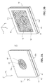
- Figure 3A shows, in perspective view, the filtering module 52, in which the top face 52a may be noted.
- Figure 3B shows, in perspective view, the filtering module 52, in which a bottom face 52b, opposite to the top face 52a, may be noted.
- the filtering module 52 comprises: a top plate 61, the exposed surface of which forms the top face 52a of the filtering module 52, lying in a plane parallel to the plane xy; a bottom plate 63, the exposed surface of which forms the bottom face 52b of the filtering module 52, lying in a respective plane which is also parallel to the plane xy; and a filter 62, set between the top plate 61 and the bottom plate 63.
- the filter 62 is set, or "sandwiched", between the top plate 61 and the bottom plate 63.
- the top plate 61 has a through opening 66, here of a circular shape, through which a portion of the filter 62 is exposed.
- the through opening 66 has dimensions such that, when the filtering module 52 is set underneath the first die 21, as shown in Figure 2 , the through opening 66 is completely contained within the acoustic chamber 6.
- the rear surface 5b of the structural layer 5 is coupled to the surface of the top plate 61 (top face 52a) that surrounds the through opening 66 on the outside.
- the through opening 66 is surrounded by a ring 68, in relief, having the function of preventing entry into the through opening 66 of any possible glue used for fixing the first die 21 and the filtering module 52 together.
- the ring 68 may be replaced by a trench, or else by a region, substantially coplanar to the top face 52a, of hydrophobic material, that is to react with water-based glues in order to prevent penetration of said glues into the through opening 66.
- both the through opening 66 and the ring 68 are completely contained within the acoustic chamber 6.
- the rear surface 5b of the structural layer 5 is coupled to the surface of the top plate 61 (top face 52a) that surrounds the ring 68 on the outside.
- the bottom plate 63 has a through opening 70, here by way of example represented as being of a square shape, through which a respective portion of the filter 62 is exposed.
- the through opening 70 has a diameter greater than the diameter of the through opening 66.
- the centre of the geometrical shape defined by the through opening 66 here, a circle
- the centre of the geometrical shape defined by the through opening 70 here, a square
- the through opening 66 is completely contained within the through opening 70.
- Figure 4 shows, by way of example, an enlarged portion of the filter 62.
- the filter 62 is a fabric made up of threads 74 that form a weave such as to define through openings 72 of maximum dimension d 1 , measured along the axis x and/or the axis y, comprised between 5 and 40 ⁇ m, in particular comprised between 15 and 25 ⁇ m.
- the threads 74 that form the weave have a thickness d 2 , measured along the axis x and/or the axis y, that is some tens of micrometers, for example approximately 40 ⁇ m.
- the filter 62 is of a material chosen according to the need, for example obtained using threads 74 of PET, or thermoplastic organic polymers such as for example polyether-ether-ketone (PEEK), or some other material.
- PEEK polyether-ether-ketone
- a fabric suitable for the purpose is commercially available and marketed under the trade name "Acoustex", manufactured by Saati S.p.A.
- the first and second plates 61, 63 are of semiconductor material, such as silicon, or else of metal material, such as stainless steel. However, any other material compatible with MEMS microprocessing and suitable to be processed to form the first and second plates 61, 63 may be used, according to the need, for example a plastic material.
- the second plate 63 is provided, and the through opening 70 is made therein (for example, with an etching step in the case of use of semiconductor material, or a punching step in the case of a plate 61 of stainless steel, or using an "injection moulding" tool to obtain a plate 63 of plastic material). Then, a layer of glue 71 is dispensed over a surface 63a of the second plate 63.
- the surface 63a is opposite to the surface of the second plate 63 that, at the end of the manufacturing process, forms the bottom face 52b of the filtering module 52.
- the layer of glue is, for example, a non-conductive epoxy glue, or silicone, and is obtained by dispensing the glue in a peripheral region of the surface 63a of the second plate 63, in such a way that the glue will not penetrate within the through opening 70.
- glue it is possible to use a biadhesive tape, appropriately shaped.
- the first plate 61 is provided and made therein is the through opening 66 (following the same procedure as the one adopted to form the opening 70 in the second plate 63).
- the ring 68 or, alternatively, the trench or the hydrophobic region, here not shown.
- a layer of glue 76 is dispensed over the surface 61b of the first plate 61.
- Said surface 61b is opposite to the surface of the first plate 6, which, at the end of manufacturing, forms the top face 52a of the filtering module 52.
- the layer of glue is, for example, a non-conductive epoxy glue, or silicone, and is formed by dispensing the glue over a peripheral region of the surface 61b of the first plate 61, in such a way that the glue does not penetrate into the through opening 66.
- a biadhesive tape appropriately shaped. In this case, the ring 68 is not necessary in so far as there is no risk of penetration of the glue into the through opening 66.
- the step of dispensing of glue over the surface 61b of the first plate 61 may further be omitted in the case where the amount of glue dispensed over the second plate 63 is such that said glue, as a result of pressure between the filter 62 and the second plate 63, flows into the through openings 72 of the filter, and reaches the opposite surface, i.e., the surface of the filter that is set in direct contact with the first plate 61. Also in this case, the ring 68 may be omitted.
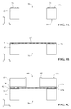
- the steps of Figures 5A-5C may be carried out simultaneously for a plurality of filtering modules 52, formed alongside one another on a same wafer of semiconductor material (or metal, or plastic material, according to respective embodiments).
- a plurality of through openings 70 are formed, alongside one another and at a distance from one another, to form for example an array structure.
- a fabric is stretched over the entire top surface of the first wafer and coupled thereto (e.g., by gluing).
- a plurality of through openings 66 are formed, alongside one another and at a distance from one another, to form the array structure.
- Integration of the filtering module 52 in the package 50 is obtained by using the known MEMS microprocessing techniques.
- the filtering module 52 is coupled to the surface 23a of the substrate 23 by glue dispensed on the rear face 52b, for example a non-conductive epoxy glue, or silicone, or else by a biadhesive tape, appropriately shaped so as not to occlude the through openings of the filter. Then, an adequate amount of glue is further dispensed on the top face 52a, alongside the through opening 66 and the ring 68 (if present), and physical coupling of the first die 21 to the filtering module 52 is carried out.
- glue it is possible to use a biadhesive tape appropriately shaped so as not to occlude the through openings of the filter.
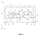
- Figure 6 shows an acoustic-transducer device 81 according to a further embodiment.
- the acoustic-transducer device 81 is similar to the acoustic-transducer device 51 of Figure 2 . Elements that are in common are thus not described further and are designated by the same reference numbers.
- the acoustic-transducer device 81 differs from the acoustic-transducer device 51 in that it has a filtering module 82 of a different type.
- the filtering module 82 is formed starting from a wafer of semiconductor material, for example silicon, appropriately processed to form, through said wafer, a plurality of through openings of dimensions such as to prevent passage of the contaminating particles that are to be blocked.
- the filtering module 82 is in the form of a membrane having a plurality of holes.
- the thickness of the filtering module 82 is comprised in the interval 80-120 ⁇ m, for example 100 ⁇ m.
- the filtering module 82 Since the filtering module 82, according to this embodiment, is of semiconductor material, it is not necessary to set it between two plates as described with reference to the filter 62 of Figures 3A and 3B , in so far as it presents good characteristics of stiffness and strength. In this case, the filtering module 82 itself constitutes the filter and is set between the acoustic chamber 6 of the first die 21 and the sound port 28 without the aid of further supporting means.
- FIG. 7 shows, in top plan view in the plane xy, a filtering module 82 that may be used in the production of the acoustic-transducer device 81, according to one embodiment of the present disclosure.
- the filtering module 82 of Figure 7 has filtering openings 84, which extend throughout the thickness of the filtering module 82, and form a serpentine path.
- Said serpentine path comprises, in particular, a plurality of sub-openings 84' of a substantially rectangular shape, which are fluidically connected together (a sub-opening 84' is represented with a dashed line in Figure 7 , so that it may be identified more clearly).
- Each sub-opening 84' has a respective main extension d MAX (major side of the rectangle) along one of the axes x or y, and a secondary extension d MIN (minor side of the rectangle) along the other between the axes x and y.
- Two consecutive sub-openings 84' fluidically coupled together form substantially an L, and a plurality of consecutive sub-openings 84' fluidically coupled together form the aforesaid serpentine geometrical shape.
- the main extension d MAX of each sub-opening 84' (length), measured along the respective reference axis x or y, has a value comprised between 30 ⁇ m and 90 ⁇ m, for example equal to 45 ⁇ m.
- the secondary extension d MIN of each sub-opening (width) has a value, measured along the respective reference axis y or x orthogonal to the respective axis x or y of main extension, in the interval comprised between 5 ⁇ m and 30 ⁇ m, more in particular between 10 ⁇ m and 20 ⁇ m, for example 15 ⁇ m.
- the filtering module 82 comprises a plurality of serpentine through openings, separated from one another, along x and y, by respective first and second intermediate interruption regions 86, 88.
- the first intermediate interruption regions 86 have a main extension parallel to the axis y
- the second intermediate interruption regions 88 have a main extension parallel to the axis x.
- the first and the second intermediate interruption regions 86, 88 are full regions, i.e., they do not have through openings, and have the function of improving the strength of the filtering module 82, in order to reduce the probability of undesired failure thereof. Also the serpentine shape described is deemed, by the present applicant, suited to guaranteeing a good filtering power together with a good resistance to failure.
- the filtering module 82 may have, as an alternative to the serpentine through openings, rounded or quadrangular holes set to form an array, or set according to any other pattern. More in general, the through openings of the filtering module 82 may have a generic geometrical shape chosen freely according to the need. In order to guarantee a good filtering, it is in any case advisable for said through openings, whatever their geometrical shape, to present a maximum dimension equal to the values indicated for d MAX .
- the ratio between the area occupied by the trench regions and the area occupied by the full regions of the portion of the filtering module 82 effectively used for the filtering purposes is chosen in the interval 1-2 (where "1" means that 50% of the area of the filtering module 82 is occupied by the filtering openings 84 and the remaining 50% of the area is occupied by the first and second intermediate interruption regions 86, 88, and "2" means that the filtering openings 84 occupy twice the area occupied by the first and second intermediate interruption regions 86, 88).
- said ratio affords a good compromise between strength of the filtering module 82 and access to the acoustic chamber 6 by sound waves coming from the environment external to the package.
- Mechanical coupling of the filtering module 82 to the base substrate 23 is obtained, according to one embodiment, by dispensing a layer of glue (not shown) over peripheral regions of the filtering module 82, in particular on both of the faces 82a, 82b of the filtering module 82 in surface regions of the faces 82a, 82b that, in use, are set in contact with the structural layer 5 of the first die 21 and, respectively, with the base substrate 23.
- the glue must not be dispensed in regions of the filtering module 82 that, in use, directly face the acoustic chamber 6 and the through opening 28.
- a biadhesive tape As an alternative to the glue, it is possible use a biadhesive tape, appropriately shaped for not occluding the through openings of the filter.
- the filtering module 82 is coupled on the base substrate 23 so that the filtering module 82 extends to cover the sound port 28 with the face 82b; then, by gluing, the first die 21 is coupled on the filtering module 82 so that the acoustic chamber 6 gives completely out onto the face 82a of the filtering module 82 and is in acoustic communication with the sound port 28 through the filtering openings 84.
- the filtering module 82 comprises a surface layer of hydrophobic material, for example silicon carbide or Teflon.
- the hydrophobic layer is obtained, for example, with the sputtering technique, after the step of etching for formation of the filtering openings 84. Since the hydrophobic layer does not require a particularly large thickness (from some hundreds of nanometres up to a few micrometers), the sputtering step carried out after formation of the through openings does not occlude said through openings significantly.
- the hydrophobic layer thus formed has the function of inhibiting entry of water into the acoustic chamber 6 of the first die 21.
- the hydrophobic layer forms the face 82b of the filtering module 82.
- Figure 8 shows an acoustic-transducer device 91, provided with a package 90, according to a further embodiment. Elements of the acoustic-transducer device 91 that are in common to the acoustic-transducer device 19 are designated by the same reference numbers and are not described any further.
- a base supporting substrate 93 (corresponding, from a structural standpoint, to the substrate 23 of Figure 1 ) supports the first and second dice 21, 22; the base supporting substrate 93 is formed by two supporting elements 94, 95 extending between which is a filter 96, in particular a filtering fabric that has the characteristics already described with reference to Figures 2 , 3A and 3B and is coupled between the two supporting elements 94, 95 in a way similar to what has been described with reference to Figures 5A-5C .
- the supporting element 94 extends between the filter 96 and the environment external to the package 90, whereas the supporting element 95 extends between the filter 96 and the cavity 8 internal to the package 90.
- the supporting element 94 is an LGA substrate (provided with the lands 29 for electrical connection towards the outside world), and the support element 95 is a generic semiconductor substrate, having purposely provided metallization layers and vias (not shown in detail) for routing the electrical signals towards the outside of the package.
- Through openings 98a and 98b extend, mutually aligned along z, through the supporting elements 94, 95 and are fluidically connected together through the filter 96.
- the through openings 98a and 98b form a sound port in a way similar to the through opening 28 described previously.
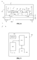
- Figure 9 shows an electronic device 100 that uses the acoustic-transducer device 51, 81, 91 according to the respective embodiment of Figures 2 , 6 , and 8 , obtained as illustrated previously in the form of SIP (System in Package).
- SIP System in Package
- the electronic device 100 comprises, in addition to the acoustic-transducer device 51, 81, 91, a microprocessor (CPU) 101, a memory block 102, connected to the microprocessor 101, and an input/output interface 103, for example a keyboard and/or a display, which is also connected to the microprocessor 101.
- a microprocessor CPU
- memory block 102 connected to the microprocessor 101
- an input/output interface 103 for example a keyboard and/or a display, which is also connected to the microprocessor 101.
- the acoustic-transducer device 51, 81, 91 communicates with the microprocessor 101, and in particular transmits the electrical signals processed by the ASIC 22' of the die 22 associated to the MEMS detection structures of the die 21.
- the electronic device 100 is, for example, a mobile communication device, such as, for instance, a cellphone, a PDA, a notebook, but also a voice recorder, an audio-file reader with voice-recording capacity, a console for videogames, a hydrophone, etc.
- a mobile communication device such as, for instance, a cellphone, a PDA, a notebook, but also a voice recorder, an audio-file reader with voice-recording capacity, a console for videogames, a hydrophone, etc.
- the assembly described enables integration, within a same package, of a MEMS acoustic transducer and a filter designed to protect said MEMS acoustic transducer from contamination of particles of dimensions equal to some micrometers, or some tens, of micrometers coming from the environment external to the package.
- the MEMS acoustic transducer in particular as regards the geometrical shape of the constitutive elements.
- the space internal to the package so allows, there may possibly be housed inside the package itself also a number of MEMS sensors in addition to the MEMS acoustic transducer, each possibly provided with a sensitive element that requires a communication towards the external environment.
- Further integrated circuits e.g., ASICs may further be provided and housed inside the same package.
Landscapes
- Engineering & Computer Science (AREA)
- Signal Processing (AREA)
- Physics & Mathematics (AREA)
- Acoustics & Sound (AREA)
- Microelectronics & Electronic Packaging (AREA)
- Manufacturing & Machinery (AREA)
- Computer Hardware Design (AREA)
- Health & Medical Sciences (AREA)
- General Health & Medical Sciences (AREA)
- Toxicology (AREA)
- Piezo-Electric Or Mechanical Vibrators, Or Delay Or Filter Circuits (AREA)
- Micromachines (AREA)
- Electrostatic, Electromagnetic, Magneto- Strictive, And Variable-Resistance Transducers (AREA)
Abstract
Description
- The present invention relates to a semiconductor integrated device, for acoustic applications, with a contamination protection element, and to the manufacturing method thereof. In particular, the semiconductor integrated device includes a MEMS acoustic transducer, and the contamination protection element is a filter adapted to protect the MEMS acoustic transducer from dust.
- In a known way, an acoustic transducer (in particular a microphone) of the MEMS (Micro-Electro-Mechanical System) type comprises a membrane sensitive structure designed to transduce acoustic-pressure waves into an electrical quantity (for example, a capacitive variation), and a reading electronics designed to carry out appropriate processing operations (amongst which amplification and filtering operations) on said electrical quantity for supplying an electrical output signal (for example, a voltage) representing the acoustic-pressure wave received. In the case where a capacitive detection principle is adopted, the microelectromechanical sensitive structure in general comprises a mobile electrode, obtained as diaphragm or membrane, set facing a fixed electrode, for providing the plates of a variable-capacitance detection capacitor. The mobile electrode is anchored by a first, generally perimetral, portion thereof to a structural layer, whereas a second portion thereof, which is generally central, is free to move or bend in response to the pressure exerted by the incident acoustic-pressure waves. The mobile electrode and the fixed electrode thus provide a capacitor, and bending of the membrane that constitutes the mobile electrode causes a variation of capacitance, as a function of the acoustic signal to be detected.
- With reference to
Figure 1 , an acoustic-transducer device 19 is represented. The acoustic-transducer device 19 comprises afirst die 21 that integrates aMEMS structure 1 provided with amembrane 2, mobile and of conductive material, which faces a rigid plate 3 (whereby is meant an element that is relatively rigid with respect to themembrane 2, which is, instead, flexible). Therigid plate 3 includes at least one conductive layer facing themembrane 2 so that themembrane 2 and therigid plate 3 form facing plates of a capacitor. - The
membrane 2, which in use undergoes deformation in response to incident acoustic-pressure waves, is at least partially suspended over astructural layer 5 and directly faces acavity 6, obtained by forming a trench in arear surface 5b of the structural layer 5 (therear portion 5b is opposite to afront surface 5a of the samestructural layer 5, set in the proximity of the membrane 2). - The
MEMS structure 1 is housed in aninternal cavity 8 of apackage 20, together with a furtherdie 22, of semiconductor material, which integrates a processing circuit, or ASIC (Application-Specific Integrated Circuit) 22'. The ASIC 22' is electrically coupled to theMEMS structure 1 by an electrical conductor 25', which connects respective pads 26' of the first andsecond dice second dice substrate 23 of thepackage 20. Thefirst die 21 is coupled to thesubstrate 23 at therear surface 5b of thestructural layer 5, for example by an adhesive layer. Likewise, also thesecond die 22 is coupled to thesubstrate 23 at arear surface 22b thereof. The ASIC 22' is provided on afront surface 22a of thesecond die 22, opposite to therear surface 22b. - Appropriate metallization layers and vias (not shown in detail) are provided in the
substrate 23 for routing the electrical signals onto the outside of thepackage 20. Furtherelectrical connections 25", obtained with the wire-bonding technique, are provided betweenpads 26" of thesecond die 22 andrespective pads 26" of thesubstrate 23. - Further coupled to the
substrate 23 is a covering 27 of thepackage 20, which encloses the first andsecond dice - Electrical-
connection elements 29, for example in the form of conductive lands, are provided at the underside of the substrate 23 (the side exposed outwards), for soldering and electrical connection to a printed-circuit board. - The
substrate 23 further has a through opening, or hole, 28, which sets in fluid communication thecavity 6 of thefirst die 21 with the environment external to thepackage 20. The through opening 28 (in what follows referred to as "sound port") enables introduction of a flow of air from outside thepackage 20 and of the acoustic-pressure waves, which, impinging upon themembrane 2, deflect it. - In a known way, the sensitivity of the acoustic transducer depends upon the mechanical characteristics of the
membrane 2 of theMEMS structure 1, and further upon the assembly of themembrane 2 and of therigid plate 3. Further, the volume of the acoustic chamber formed by thecavity 6 directly affects the acoustic performance, determining the resonance frequency of the acoustic transducer. - Thus, multiple constraints are imposed on assembly of a MEMS acoustic transducer, which render design thereof particularly problematical, in particular where extremely compact dimensions are required, as, for example, in the case of portable applications.
- In order to protect the
cavity 6 and themembrane 2 at least partially from dust and/or water and/or other debris that might penetrate through the through opening 28 thus reducing the useful dimensions of thecavity 6, and thus jeopardizing the performance of the acoustic transducer, it is known to provide a filter (illustrated only schematically inFigure 1 , and designated by the reference 30) outside thepackage 20 and facing the sound port 28 (at a distance therefrom). Thisfilter 30 is, for example, coupled to a protective shell of a portable device (e.g., a cellphone) that houses thepackage 20. - In particular, in the case of portable applications, the
package 20 is housed inside the protective shell of the portable device itself in such a way that thesound port 28 in turn faces a respective through opening, or hole, made through the protective shell of the portable device by interposition of thefilter 30 itself. The filters currently used are mounted manually on the protective shell of the portable device and consequently present excessive dimensions with respect to the actual operating need, which is to protect exclusively thecavity 6, in addition, obviously, to themembrane 2 and therigid plate 3. - Further, the
filter 30 prevents entry of contaminating particles through the hole made through the protective shell of the portable device, but does not solve the problem of contamination deriving from particles of dust or other debris coming from various sources (for example, on account of a not perfectly hermetic closing of the protective shell). In particular, filters of the known type are altogether ineffective in regard to protection from contaminating agents during intermediate manufacturing and assembly steps, i.e., during steps of assembly of the package in the portable device. - The aim of the present invention is to provide a solution to the problems illustrated previously.
- According to the present invention a semiconductor integrated device with contamination protection element and a manufacturing method thereof are consequently provided, as defined in the annexed claims.
- For a better understanding of the present invention, preferred embodiments thereof are now described, purely by way of non-limiting example and with reference to the attached drawings, wherein:
-
Figure 1 shows a schematic cross-sectional view of a semiconductor integrated device including a MEMS acoustic transducer with the package thereof, according to an embodiment of a known type; -
Figure 2 shows a schematic cross-sectional view of a semiconductor integrated device including a MEMS acoustic transducer with the package thereof, according to one embodiment of the present invention; -
Figures 3A and 3B show a perspective view of a filtering module that may be coupled to a portion of the semiconductor integrated device ofFigure 2 , according to one embodiment of the present invention; -
Figure 4 shows an enlarged detail of a filter belonging to the filtering module ofFigures 3A and 3B ; -
Figures 5A-5C show, in lateral section, steps for manufacturing the filtering module ofFigures 3A and 3B ; -
Figure 6 shows a schematic cross-sectional view of a semiconductor integrated device including a MEMS acoustic transducer with the package thereof, according to a further embodiment of the present invention; -
Figure 7 shows a filtering module that may be coupled to a portion of the semiconductor integrated device ofFigure 6 , according to the respective embodiment; -
Figure 8 shows a schematic cross-sectional view of a semiconductor integrated device including a MEMS acoustic transducer with the package thereof, according to a further embodiment of the present invention; and -
Figure 9 shows an electronic device including a semiconductor integrated device according to any one of the embodiments ofFigures 2 ,6 , and9 . -
Figure 2 shows, in cross-sectional view, an acoustic-transducer device 51 according to one aspect of the present disclosure. Elements that are common to the acoustic-transducer device 51 ofFigure 2 and to the acoustic-transducer device 19 ofFigure 1 are designated by the same reference numbers and are not described any further. - In greater detail, the acoustic-
transducer device 51 ofFigure 2 includes apackage 50, formed by thebase substrate 23 and by the coveringelement 27. The latter has a substantially cup-shaped conformation and is coupled to thebase substrate 23 to form the cavity, or internal space, 8 of thepackage 50. Made throughout the thickness of thebase substrate 23 is the through opening 28, which is designed to set thecavity 6 of thefirst die 21 in acoustic communication with the environment external to thepackage 50. In what follows, the through opening 28 will also be referred to as "sound port", and thecavity 6 of thefirst die 21 will also be referred to as "acoustic chamber". Further, the term "acoustic communication" is here used with the meaning of "direct acoustic communication", in the sense that generic sound waves, or acoustic-pressure waves, propagate in the environment considered using as only propagation medium air (or a possible gas, or mixture of gases, equivalent from the standpoint of propagation of sound). - The extension (in the horizontal plane xy) of the
acoustic chamber 6 is greater than the extension thereof (once again in the horizontal plane xy) of thesound port 28, in such a way that thesound port 28 will communicate entirely with theacoustic chamber 6 without giving directly out into theinternal space 8 of thepackage 50. - According to one aspect of the present disclosure, the
acoustic chamber 6 of thefirst die 21 is in acoustic communication with thesound port 28 exclusively through afiltering module 52, which is set between thesound port 28 and theacoustic chamber 6 of thefirst die 21. - The
first die 21, which houses theMEMS structure 1, is set on atop side 52a of thefiltering module 52, in particular in such a way that theacoustic chamber 6 directly faces thefiltering module 52. Thus, thefiltering module 52 creates an obstacle for passage of dust and/or contaminating particles, coming from the environment external to thepackage 50, towards theacoustic chamber 6. Thefiltering module 52 has a plurality of through openings such that the flow of air and sound waves is not interrupted or sensibly degraded by the presence of thefiltering module 52 itself. Acoustic communication of theacoustic chamber 6 towards the outside of thepackage 50 is thus guaranteed. - The
base substrate 23 is, for example, constituted by a multilayer structure, made up of one or more layers of conductive material (generally metal) separated by one or more dielectric layers (for example, constituted by a bismaldehide-triazine - BT - laminate).Electrical paths 49 are provided through thebase substrate 23 for connecting aninner surface 23a thereof, facing theinternal space 8, to anouter surface 23b thereof, facing the external environment, that carries the electrical-connection elements 29. The latter are provided, in particular, in the form of lands (in the case of packages of the so-called LGA - Land-Grid Array - type, as is the case illustrated inFigure 2 ). Alternatively, thelands 29 may be replaced by an array of "balls" or "bumps", thus providing a so-called BGA (Ball-Grid Array) package. - According to a different embodiment, the
base substrate 23 does not comprise metal layers or conductive material in general and, for example, is of plastic material. - The covering
element 27 may also be constituted by a multilayer, for example including one or more plastic and/or metal layers, and may advantageously present a metal coating (not illustrated) on an owninner surface 27a, facing theinternal space 8, for providing an electromagnetic display. Alternatively, thecovering element 27 is of metal. - The covering
element 27 is further coupled to thebase substrate 23 for sealing theinternal space 8 hermetically. -
Figure 3A shows, in perspective view, thefiltering module 52, in which thetop face 52a may be noted.Figure 3B shows, in perspective view, thefiltering module 52, in which abottom face 52b, opposite to thetop face 52a, may be noted. - With joint reference to
Figures 3A and 3B , thefiltering module 52 comprises: atop plate 61, the exposed surface of which forms thetop face 52a of thefiltering module 52, lying in a plane parallel to the plane xy; abottom plate 63, the exposed surface of which forms thebottom face 52b of thefiltering module 52, lying in a respective plane which is also parallel to the plane xy; and afilter 62, set between thetop plate 61 and thebottom plate 63. In other words, thefilter 62 is set, or "sandwiched", between thetop plate 61 and thebottom plate 63. - With reference to
Figure 3A , thetop plate 61 has a throughopening 66, here of a circular shape, through which a portion of thefilter 62 is exposed. The throughopening 66 has dimensions such that, when thefiltering module 52 is set underneath thefirst die 21, as shown inFigure 2 , the throughopening 66 is completely contained within theacoustic chamber 6. In other words, therear surface 5b of thestructural layer 5 is coupled to the surface of the top plate 61 (top face 52a) that surrounds the through opening 66 on the outside. - Optionally, the through
opening 66 is surrounded by aring 68, in relief, having the function of preventing entry into the through opening 66 of any possible glue used for fixing thefirst die 21 and thefiltering module 52 together. Thering 68 may be replaced by a trench, or else by a region, substantially coplanar to thetop face 52a, of hydrophobic material, that is to react with water-based glues in order to prevent penetration of said glues into the throughopening 66. In this case, when thefiltering module 52 is set underneath thefirst die 21 as inFigure 2 , both the throughopening 66 and thering 68 are completely contained within theacoustic chamber 6. In other words, therear surface 5b of thestructural layer 5 is coupled to the surface of the top plate 61 (top face 52a) that surrounds thering 68 on the outside. - With reference to
Figure 3B , also thebottom plate 63 has a throughopening 70, here by way of example represented as being of a square shape, through which a respective portion of thefilter 62 is exposed. The throughopening 70 has a diameter greater than the diameter of the throughopening 66. In particular, the centre of the geometrical shape defined by the through opening 66 (here, a circle) and the centre of the geometrical shape defined by the through opening 70 (here, a square), are located on a same axis z orthogonal to the plane xy. In other words, observing the throughopening 66 and the throughopening 70 in the plane xy, it may be noted that the throughopening 66 is completely contained within the throughopening 70. -
Figure 4 shows, by way of example, an enlarged portion of thefilter 62. In this embodiment, thefilter 62 is a fabric made up ofthreads 74 that form a weave such as to define throughopenings 72 of maximum dimension d1, measured along the axis x and/or the axis y, comprised between 5 and 40 µm, in particular comprised between 15 and 25 µm. Thethreads 74 that form the weave have a thickness d2, measured along the axis x and/or the axis y, that is some tens of micrometers, for example approximately 40 µm. - The
filter 62 is of a material chosen according to the need, for example obtained usingthreads 74 of PET, or thermoplastic organic polymers such as for example polyether-ether-ketone (PEEK), or some other material. A fabric suitable for the purpose is commercially available and marketed under the trade name "Acoustex", manufactured by Saati S.p.A. - The first and
second plates second plates - With reference to the steps for manufacturing the
filtering module 52, these are illustrated by way of example with reference toFigures 5A-5C , which show a lateral-sectional view, taken along the line of cross-section V-V ofFigure 3A , of thefiltering module 52 during processing steps. - With reference to
Figure 5A , thesecond plate 63 is provided, and the throughopening 70 is made therein (for example, with an etching step in the case of use of semiconductor material, or a punching step in the case of aplate 61 of stainless steel, or using an "injection moulding" tool to obtain aplate 63 of plastic material). Then, a layer ofglue 71 is dispensed over asurface 63a of thesecond plate 63. Thesurface 63a is opposite to the surface of thesecond plate 63 that, at the end of the manufacturing process, forms thebottom face 52b of thefiltering module 52. The layer of glue is, for example, a non-conductive epoxy glue, or silicone, and is obtained by dispensing the glue in a peripheral region of thesurface 63a of thesecond plate 63, in such a way that the glue will not penetrate within the throughopening 70. On the other hand, it may be noted that, even in the case where a modest amount of glue were to penetrate into the throughopening 70, this would not constitute a problem. As an alternative to glue, it is possible to use a biadhesive tape, appropriately shaped. - There is then provided (
Figure 5B ) a fabric of the type previously described, and the fabric is cut to form thefilter 62. The fabric is cut so that it will assume, in the plane xy, the perimetral shape and dimensions of thetop surface 63a of thesecond plate 63. Thefilter 62 thus formed is then stretched, and the layer ofglue 71 is brought into contact with thefilter 62, and gluing is carried out. - As an alternative to what has been described, it is further possible to stretch the fabric, and glue it to the
second plate 63 prior to cutting of the fabric itself. In this case, cutting of the fabric is carried afterwards, in any one of the subsequent manufacturing steps. - Then (
Figure 5C ), thefirst plate 61 is provided and made therein is the through opening 66 (following the same procedure as the one adopted to form theopening 70 in the second plate 63). In this step, it is further possible to form the ring 68 (or, alternatively, the trench or the hydrophobic region, here not shown). - Then, a layer of
glue 76 is dispensed over thesurface 61b of thefirst plate 61. Saidsurface 61b is opposite to the surface of thefirst plate 6, which, at the end of manufacturing, forms thetop face 52a of thefiltering module 52. The layer of glue is, for example, a non-conductive epoxy glue, or silicone, and is formed by dispensing the glue over a peripheral region of thesurface 61b of thefirst plate 61, in such a way that the glue does not penetrate into the throughopening 66. Alternatively, it is further possible to use a biadhesive tape, appropriately shaped. In this case, thering 68 is not necessary in so far as there is no risk of penetration of the glue into the throughopening 66. - The step of dispensing of glue over the
surface 61b of thefirst plate 61 may further be omitted in the case where the amount of glue dispensed over thesecond plate 63 is such that said glue, as a result of pressure between thefilter 62 and thesecond plate 63, flows into the throughopenings 72 of the filter, and reaches the opposite surface, i.e., the surface of the filter that is set in direct contact with thefirst plate 61. Also in this case, thering 68 may be omitted. - The
filtering module 52 ofFigures 3A and 3B is thus obtained. - It is evident that, in a per se known manner, the steps of
Figures 5A-5C may be carried out simultaneously for a plurality offiltering modules 52, formed alongside one another on a same wafer of semiconductor material (or metal, or plastic material, according to respective embodiments). In this case, in a way not shown in the figure, in a wafer a plurality of throughopenings 70 are formed, alongside one another and at a distance from one another, to form for example an array structure. Then a fabric is stretched over the entire top surface of the first wafer and coupled thereto (e.g., by gluing). Then, in a respective further wafer, a plurality of throughopenings 66 are formed, alongside one another and at a distance from one another, to form the array structure. The two wafers are then coupled together (as described with reference toFigure 5C ), thus fixing the fabric in between. Finally, a cutting step is carried out, for isolating a plurality offiltering modules 62 of the type shown inFigures 3A and 3B . - Integration of the
filtering module 52 in thepackage 50 is obtained by using the known MEMS microprocessing techniques. - In greater detail, after the
base substrate 23 has been processed (in particular after thesound port 28 is formed), thefiltering module 52 is coupled to thesurface 23a of thesubstrate 23 by glue dispensed on therear face 52b, for example a non-conductive epoxy glue, or silicone, or else by a biadhesive tape, appropriately shaped so as not to occlude the through openings of the filter. Then, an adequate amount of glue is further dispensed on thetop face 52a, alongside the throughopening 66 and the ring 68 (if present), and physical coupling of thefirst die 21 to thefiltering module 52 is carried out. As an alternative to the glue, it is possible to use a biadhesive tape appropriately shaped so as not to occlude the through openings of the filter. - The structure of
Figure 2 is thus obtained, in which thefirst die 21 is housed in thecavity 8 of thepackage 51 over thefiltering module 52, and theacoustic chamber 6 is in acoustic communication with the environment external to thepackage 51 via thefilter 62. -
Figure 6 shows an acoustic-transducer device 81 according to a further embodiment. - The acoustic-
transducer device 81 is similar to the acoustic-transducer device 51 ofFigure 2 . Elements that are in common are thus not described further and are designated by the same reference numbers. - The acoustic-
transducer device 81 differs from the acoustic-transducer device 51 in that it has afiltering module 82 of a different type. In particular, thefiltering module 82 is formed starting from a wafer of semiconductor material, for example silicon, appropriately processed to form, through said wafer, a plurality of through openings of dimensions such as to prevent passage of the contaminating particles that are to be blocked. In other words, thefiltering module 82 is in the form of a membrane having a plurality of holes. The thickness of thefiltering module 82 is comprised in the interval 80-120 µm, for example 100 µm. - Since the
filtering module 82, according to this embodiment, is of semiconductor material, it is not necessary to set it between two plates as described with reference to thefilter 62 ofFigures 3A and 3B , in so far as it presents good characteristics of stiffness and strength. In this case, thefiltering module 82 itself constitutes the filter and is set between theacoustic chamber 6 of thefirst die 21 and thesound port 28 without the aid of further supporting means. -
Figure 7 shows, in top plan view in the plane xy, afiltering module 82 that may be used in the production of the acoustic-transducer device 81, according to one embodiment of the present disclosure. Thefiltering module 82 ofFigure 7 hasfiltering openings 84, which extend throughout the thickness of thefiltering module 82, and form a serpentine path. Said serpentine path comprises, in particular, a plurality of sub-openings 84' of a substantially rectangular shape, which are fluidically connected together (a sub-opening 84' is represented with a dashed line inFigure 7 , so that it may be identified more clearly). Each sub-opening 84' has a respective main extension dMAX (major side of the rectangle) along one of the axes x or y, and a secondary extension dMIN (minor side of the rectangle) along the other between the axes x and y. - Two consecutive sub-openings 84' fluidically coupled together form substantially an L, and a plurality of consecutive sub-openings 84' fluidically coupled together form the aforesaid serpentine geometrical shape.
- More in particular, the main extension dMAX of each sub-opening 84' (length), measured along the respective reference axis x or y, has a value comprised between 30 µm and 90 µm, for example equal to 45 µm. The secondary extension dMIN of each sub-opening (width) has a value, measured along the respective reference axis y or x orthogonal to the respective axis x or y of main extension, in the interval comprised between 5 µm and 30 µm, more in particular between 10 µm and 20 µm, for example 15 µm.
- The
filtering module 82 comprises a plurality of serpentine through openings, separated from one another, along x and y, by respective first and secondintermediate interruption regions intermediate interruption regions 86 have a main extension parallel to the axis y, and the secondintermediate interruption regions 88 have a main extension parallel to the axis x. - The first and the second
intermediate interruption regions filtering module 82, in order to reduce the probability of undesired failure thereof. Also the serpentine shape described is deemed, by the present applicant, suited to guaranteeing a good filtering power together with a good resistance to failure. - It is however evident that other embodiments may be provided for the
filtering module 82, for example having, as an alternative to the serpentine through openings, rounded or quadrangular holes set to form an array, or set according to any other pattern. More in general, the through openings of thefiltering module 82 may have a generic geometrical shape chosen freely according to the need. In order to guarantee a good filtering, it is in any case advisable for said through openings, whatever their geometrical shape, to present a maximum dimension equal to the values indicated for dMAX. - In order to guarantee good filtering and at the same time good strength of the
filtering module 82, the ratio between the area occupied by the trench regions and the area occupied by the full regions of the portion of thefiltering module 82 effectively used for the filtering purposes (i.e., of the portion of thefiltering module 82 directly facing theacoustic chamber 6 of the first die 21) is chosen in the interval 1-2 (where "1" means that 50% of the area of thefiltering module 82 is occupied by thefiltering openings 84 and the remaining 50% of the area is occupied by the first and secondintermediate interruption regions filtering openings 84 occupy twice the area occupied by the first and secondintermediate interruption regions 86, 88). The present applicant has noted that said ratio affords a good compromise between strength of thefiltering module 82 and access to theacoustic chamber 6 by sound waves coming from the environment external to the package. - Mechanical coupling of the
filtering module 82 to thebase substrate 23 is obtained, according to one embodiment, by dispensing a layer of glue (not shown) over peripheral regions of thefiltering module 82, in particular on both of thefaces filtering module 82 in surface regions of thefaces structural layer 5 of thefirst die 21 and, respectively, with thebase substrate 23. In a per se known manner, the glue must not be dispensed in regions of thefiltering module 82 that, in use, directly face theacoustic chamber 6 and the throughopening 28. - As an alternative to the glue, it is possible use a biadhesive tape, appropriately shaped for not occluding the through openings of the filter.
- Then, by gluing, the
filtering module 82 is coupled on thebase substrate 23 so that thefiltering module 82 extends to cover thesound port 28 with theface 82b; then, by gluing, thefirst die 21 is coupled on thefiltering module 82 so that theacoustic chamber 6 gives completely out onto theface 82a of thefiltering module 82 and is in acoustic communication with thesound port 28 through thefiltering openings 84. - It is evident that it is possible, as an alternative, to couple together the
first die 21 and thefiltering module 82 prior to the step of coupling of thefiltering module 82 to thebase substrate 23. - Relative coupling between the through
opening 28, thefiltering module 82, and thefirst die 21 shown inFigure 6 is thus obtained. - According to a further embodiment of the
filtering module 82, the latter comprises a surface layer of hydrophobic material, for example silicon carbide or Teflon. The hydrophobic layer is obtained, for example, with the sputtering technique, after the step of etching for formation of thefiltering openings 84. Since the hydrophobic layer does not require a particularly large thickness (from some hundreds of nanometres up to a few micrometers), the sputtering step carried out after formation of the through openings does not occlude said through openings significantly. - The hydrophobic layer thus formed has the function of inhibiting entry of water into the
acoustic chamber 6 of thefirst die 21. For this purpose, it is sufficient for the hydrophobic layer to extend alongside thefiltering module 82 facing the outside of thepackage 50. In this case, the hydrophobic layer forms theface 82b of thefiltering module 82. -
Figure 8 shows an acoustic-transducer device 91, provided with apackage 90, according to a further embodiment. Elements of the acoustic-transducer device 91 that are in common to the acoustic-transducer device 19 are designated by the same reference numbers and are not described any further. According to the embodiment ofFigure 8 , a base supporting substrate 93 (corresponding, from a structural standpoint, to thesubstrate 23 ofFigure 1 ) supports the first andsecond dice base supporting substrate 93 is formed by two supportingelements filter 96, in particular a filtering fabric that has the characteristics already described with reference toFigures 2 ,3A and 3B and is coupled between the two supportingelements Figures 5A-5C . The supportingelement 94 extends between thefilter 96 and the environment external to thepackage 90, whereas the supportingelement 95 extends between thefilter 96 and thecavity 8 internal to thepackage 90. - According to one embodiment, the supporting
element 94 is an LGA substrate (provided with thelands 29 for electrical connection towards the outside world), and thesupport element 95 is a generic semiconductor substrate, having purposely provided metallization layers and vias (not shown in detail) for routing the electrical signals towards the outside of the package. - Through
openings elements filter 96. The throughopenings opening 28 described previously. -
Figure 9 shows anelectronic device 100 that uses the acoustic-transducer device Figures 2 ,6 , and8 , obtained as illustrated previously in the form of SIP (System in Package). - The
electronic device 100 comprises, in addition to the acoustic-transducer device memory block 102, connected to themicroprocessor 101, and an input/output interface 103, for example a keyboard and/or a display, which is also connected to themicroprocessor 101. - The acoustic-
transducer device microprocessor 101, and in particular transmits the electrical signals processed by the ASIC 22' of the die 22 associated to the MEMS detection structures of thedie 21. - The
electronic device 100 is, for example, a mobile communication device, such as, for instance, a cellphone, a PDA, a notebook, but also a voice recorder, an audio-file reader with voice-recording capacity, a console for videogames, a hydrophone, etc. - The advantages of the assembly proposed for an integrated acoustic device emerge clearly from the foregoing description.
- In particular, it is once again emphasized that the assembly described enables integration, within a same package, of a MEMS acoustic transducer and a filter designed to protect said MEMS acoustic transducer from contamination of particles of dimensions equal to some micrometers, or some tens, of micrometers coming from the environment external to the package.
- It is thus possible to reduce the occupation of space and provide a complete system, having a filtering function, within a single package.
- Finally, it is clear that modifications and variations may be made to what has been described and illustrated herein, without thereby departing from the scope of the present invention, as defined in the annexed claims.
- In particular, as already highlighted, there may be envisaged a different configuration of the MEMS acoustic transducer, in particular as regards the geometrical shape of the constitutive elements. In the case where the space internal to the package so allows, there may possibly be housed inside the package itself also a number of MEMS sensors in addition to the MEMS acoustic transducer, each possibly provided with a sensitive element that requires a communication towards the external environment. Further integrated circuits (e.g., ASICs) may further be provided and housed inside the same package.
Claims (17)
- A semiconductor integrated device (51, 81; 91), comprising:- a package (50) having a base element (23) and a covering element (27) jointly defining an internal space (8) of the package (50), said base element (23) having an acoustic-access opening (28; 98b) in acoustic communication with an environment external to the package (50); and- a MEMS acoustic transducer (21), housed in the internal space (8) of said package (50) and provided with an acoustic chamber (6) facing the acoustic-access opening (28; 98b),
characterized in that it further comprises a filtering module (52; 82; 96), adapted to inhibit passage of contaminating particles having dimensions larger than a filtering dimension (d1; dMIN; dMAX), set between the MEMS acoustic transducer (21) and the acoustic-access opening (28; 98b), said filtering module forming at least one direct acoustic path between the acoustic-access opening (28; 98b) and the acoustic chamber (6). - An integrated device according to claim 2, wherein said filtering dimension is comprised between 10 µm and 35 µm.
- An integrated device according to claim 1 or claim 2, wherein said filtering module (52; 96) includes a filtering fabric (62) having a plurality of threads (74) interwoven according to a pattern that defines through openings (72) of maximum dimension equal to said filtering dimension (d1).
- An integrated device according to any one of the preceding claims, wherein the base element (23) comprises a first substrate (94) having said acoustic-access opening (98b) that extends throughout the thickness of the first substrate (94), and a second substrate (95) having a hole (98a) that extends throughout the thickness of the second substrate (95), said filtering fabric (62) being integrated in the base element (23) between the first and second substrates (94, 95),
wherein the first substrate, the second substrate, and the filtering fabric (62) are coupled together in such a way that the acoustic-access opening (98b) and the hole (98, 98a) are in direct acoustic connection with one another by means of the through openings (72) of the filtering fabric (62). - An integrated device according to claim 3, wherein the filtering module (52) includes a first supporting plate (61) and a second supporting plate (63) provided with respective first and second windows (66, 70), said filtering fabric (62) being set between the first and second supporting plates (61, 63) in such a way that the first and second windows (66, 70) expose the same through openings (72) of the filtering fabric (62),
and wherein the filtering module (52) is completely housed in the internal space (8) of the package (50) so that the through openings (72) directly face the acoustic chamber (6) and the acoustic-access opening (28), thus defining a direct acoustic path for an acoustic wave that propagates from the acoustic-access opening (28) to the acoustic chamber (6) through the second window (63), the first window (61), and the through openings (72). - An integrated device according to claim 1 or 2, wherein said filtering module (82) is provided in the form of membrane of semiconductor material having a plurality of through openings (84),
said filtering module (82) being completely housed in the internal space (8) of the package (50) so that the through openings (84) directly face the acoustic chamber (6) and to the acoustic-access opening (28), thus defining a direct acoustic path for an acoustic wave that propagates from the acoustic-access opening (28) to the acoustic chamber (6) through said through openings (84). - An integrated device according to claim 6, wherein said through openings (84) have a serpentine profile.
- An integrated device according to any one of the preceding claims, wherein the MEMS acoustic transducer (21) includes a structural layer (5) having a front surface (5a) provided on which is a membrane (2) that is to bend as a result of sound waves, and a rear portion (5b), from which, through said structural layer (5), said acoustic chamber (6) extends until it reaches said membrane (2); and wherein the rear portion (5b) of said structural layer (5) is coupled to said filtering module (52; 82; 96) and, via the latter, to an inner wall (23a) of said base element (23) surrounding said acoustic-access opening (28).
- An integrated device according to any one of the preceding claims, wherein said package (50) further houses, in the internal space (8), a second die (22) integrating a first ASIC electronic circuit (22') functionally coupled to the MEMS acoustic transducer (21) for receiving and processing a signal transduced by the MEMS acoustic transducer (21) as a function of an acoustic-pressure wave received by the MEMS acoustic transducer (21) through said direct acoustic path.
- An integrated device according to any one of the preceding claims wherein said filtering module (52; 82; 96), along said direct acoustic path, is hydrophobic.
- An electronic device (100), comprising an integrated device according to any one of claims 1 to 10, said electronic device being chosen in the group comprising: a cellphone, a PDA, a notebook, a voice recorder, an audio-file reader with voice-recorder function, a console for videogames, and a hydrophone.
- A method for assembly of a semiconductor integrated device, comprising:- providing a package (50) having a base element (23) and a covering element (27) that are to define jointly an internal space (8) of the package (50), said base element (23) having an acoustic-access opening (28; 98b) in acoustic communication with an environment external to the package (50); and- housing a MEMS acoustic transducer (21), provided with an acoustic chamber (6), in the internal space (8) of said package (50) in such a way that the acoustic chamber (6) faces the acoustic-access opening (28; 98b),characterized in that it further comprises the steps of:- arranging a filtering module (52; 82; 96), adapted to inhibit passage of contaminating particles having dimensions larger than a filtering dimension (d1; dMIN; dMAX), between the MEMS acoustic transducer (21) and the acoustic-access opening (28; 98b); and- forming at least one direct acoustic path between the acoustic-access opening (28; 98b) and the acoustic chamber (6) through the filtering module (52; 82; 96).
- A method according to claim 12, wherein the step of providing the filtering module comprises housing, between the MEMS acoustic transducer (21) and the acoustic-access opening (28; 98b), a filtering fabric (62) having a plurality of threads (74) interwoven according to a pattern that defines through openings (72) of a maximum dimension equal to said filtering dimension (d1).
- A method according to claim 13, wherein the base element (23) comprises a first substrate (94) having said acoustic-access opening (98b) that extends throughout the thickness of the first substrate (94), and a second substrate (95) having a hole (98a) that extends throughout the thickness of the second substrate (95),
the step of providing the filtering module comprising the steps of:integrating said filtering fabric (62) in the base element (23) between the first and second substrates (94, 95),coupling together the first substrate, the second substrate, and the filtering fabric in such a way that the acoustic-access opening (98b) and the hole (98, 98a) are in direct acoustic connection with one another through the through openings (72) of the filtering fabric (62). - A method according to claim 13, further comprising the step of manufacturing said filtering module, including the sub-steps of:- providing a first supporting plate (61);- providing a second supporting plate (63);- forming a first window (66) in the first supporting plate (61);- forming a second window (70) in the second supporting plate (63); and- setting the filtering fabric (62) between the first supporting plate (61) and the second supporting plate (63) in such a way that the first window (66) and the second window (70) expose the same through openings (72) of the filtering fabric (62), thus defining a direct acoustic path for a acoustic wave that propagates from the second window (63) to the first window (61) through said through openings (72).
- A method according to claim 12, further comprising the steps of:- manufacturing said filtering module by processing a semiconductor wafer for form a membrane of semiconductor material having a plurality of through openings (84); and- housing said filtering module in the internal space (8) of the package (50) so that the through openings (84) directly face the acoustic chamber (6) and the acoustic-access opening (28), thus defining a direct acoustic path for an acoustic wave that propagates from the acoustic-access opening (28) to the acoustic chamber (6) through the through openings (84).
- A method according to claim 16, wherein said through openings (84) have a serpentine profile.
Applications Claiming Priority (1)
| Application Number | Priority Date | Filing Date | Title |
|---|---|---|---|
| ITTO20150148 | 2015-03-05 |
Publications (1)
| Publication Number | Publication Date |
|---|---|
| EP3065416A1 true EP3065416A1 (en) | 2016-09-07 |
Family
ID=53053038
Family Applications (1)
| Application Number | Title | Priority Date | Filing Date |
|---|---|---|---|
| EP15200515.3A Withdrawn EP3065416A1 (en) | 2015-03-05 | 2015-12-16 | Semiconductor integrated device for acoustic applications with contamination protection element, and manufacturing method thereof |
Country Status (3)
| Country | Link |
|---|---|
| US (1) | US9769554B2 (en) |
| EP (1) | EP3065416A1 (en) |
| CN (2) | CN205590278U (en) |
Cited By (5)
| Publication number | Priority date | Publication date | Assignee | Title |
|---|---|---|---|---|
| WO2018197838A1 (en) * | 2017-04-28 | 2018-11-01 | Cirrus Logic International Semiconductor Limited | Mems devices and processes |
| GB2563461A (en) * | 2017-06-16 | 2018-12-19 | Cirrus Logic Int Semiconductor Ltd | Transducer packaging |
| EP3457709A1 (en) | 2017-09-15 | 2019-03-20 | STMicroelectronics S.r.l. | Method for manufacturing a thin filtering membrane, acoustic transducer device including the filtering membrane, method for assembling the acoustic transducer device, and electronic system |
| WO2019060599A1 (en) * | 2017-09-21 | 2019-03-28 | Knowles Electronics, Llc | Elevated mems device in a microphone with ingress protection |
| EP4380182A1 (en) * | 2022-12-01 | 2024-06-05 | Infineon Technologies AG | Monolithic integration of mems sound transducer and environmental barrier |
Families Citing this family (30)
| Publication number | Priority date | Publication date | Assignee | Title |
|---|---|---|---|---|
| US9769554B2 (en) * | 2015-03-05 | 2017-09-19 | Stmicroelectronics (Malta) Ltd | Semiconductor integrated device for acoustic applications with contamination protection element, and manufacturing method thereof |
| US10291973B2 (en) * | 2015-05-14 | 2019-05-14 | Knowles Electronics, Llc | Sensor device with ingress protection |
| US10278281B1 (en) * | 2015-10-30 | 2019-04-30 | Garmin International, Inc. | MEMS stress isolation and stabilization system |
| US10861796B2 (en) | 2016-05-10 | 2020-12-08 | Texas Instruments Incorporated | Floating die package |
| WO2018064803A1 (en) * | 2016-10-08 | 2018-04-12 | Goertek. Inc | Mems microphone device and electronics apparatus |
| GB2555659B (en) * | 2016-11-07 | 2020-01-15 | Cirrus Logic Int Semiconductor Ltd | Package for MEMS device and process |
| US10179730B2 (en) * | 2016-12-08 | 2019-01-15 | Texas Instruments Incorporated | Electronic sensors with sensor die in package structure cavity |
| DE102016124270A1 (en) * | 2016-12-13 | 2018-06-14 | Infineon Technologies Ag | SEMICONDUCTOR PACKAGE AND METHOD FOR MANUFACTURING A SEMICONDUCTOR PACKAGE |
| WO2018218509A1 (en) * | 2017-05-31 | 2018-12-06 | Goertek.Inc | A mems microphone and a manufacturing method thereof |
| DE102017115405B3 (en) | 2017-07-10 | 2018-12-20 | Epcos Ag | MEMS microphone with improved particle filter |
| WO2019099414A1 (en) * | 2017-11-14 | 2019-05-23 | Knowles Electronics, Llc | Sensor package with ingress protection |
| DE102018200190B4 (en) * | 2018-01-08 | 2019-08-14 | Infineon Technologies Ag | Microelectromechanical system with filter structure |
| IT201800002049A1 (en) | 2018-01-26 | 2019-07-26 | St Microelectronics Srl | MANUFACTURING METHOD OF A SEMICONDUCTOR PLATE EQUIPPED WITH A THIN FILTER MODULE, SEMICONDUCTOR PLATE INCLUDING THE FILTER MODULE, PACKAGE HOUSING THE SEMICONDUCTOR PLATE, AND ELECTRONIC SYSTEM |
| DE102018203098B3 (en) * | 2018-03-01 | 2019-06-19 | Infineon Technologies Ag | MEMS sensor |
| EP3654053A1 (en) * | 2018-11-14 | 2020-05-20 | Infineon Technologies AG | Package with acoustic sensing device(s) and millimeter wave sensing elements |
| US11711641B2 (en) | 2019-04-10 | 2023-07-25 | Knowles Electronics, Llc | RF immune microphone |
| CN210156374U (en) * | 2019-09-29 | 2020-03-17 | 青岛歌尔智能传感器有限公司 | System-in-package structure and electronic device |
| CN111918191A (en) * | 2020-07-24 | 2020-11-10 | 钰太芯微电子科技(上海)有限公司 | Combined packaged microphone |
| US11943585B2 (en) | 2021-01-14 | 2024-03-26 | xMEMS Labs, Inc. | Air-pulse generating device with common mode and differential mode movement |
| US12261567B2 (en) | 2021-01-14 | 2025-03-25 | xMEMS Labs, Inc. | Demodulation signal generator for air pulse generator |
| US12262177B2 (en) | 2021-01-14 | 2025-03-25 | xMEMS Labs, Inc. | Air-pulse generating device producing asymmetric air pulses |
| US12356141B2 (en) | 2021-01-14 | 2025-07-08 | xMEMS Labs, Inc. | Air-pulse generating device, wearable sound device, bladeless fan, and airflow producing method |
| US12309548B2 (en) * | 2021-01-14 | 2025-05-20 | xMEMS Labs, Inc. | Air-pulse generating device with efficient propagation |
| US12075213B2 (en) * | 2021-01-14 | 2024-08-27 | xMEMS Labs, Inc. | Air-pulse generating device |
| CN113200510B (en) * | 2021-04-29 | 2024-10-11 | 日月光半导体制造股份有限公司 | Semiconductor structure |
| EP4727157A2 (en) * | 2021-05-11 | 2026-04-15 | Infineon Technologies AG | Sound transducer device comprising an environmental barrier |
| EP4283610B1 (en) * | 2022-05-28 | 2025-08-27 | xMEMS Labs, Inc. | Air-pulse generating device with efficient propagation |
| CN115914961B (en) * | 2022-11-17 | 2025-10-21 | 歌尔微电子股份有限公司 | sensor |
| DE102023209592A1 (en) | 2023-09-29 | 2025-04-03 | Robert Bosch Gesellschaft mit beschränkter Haftung | Manufacturing method for a micromechanical sensor component and corresponding micromechanical sensor component |
| US20250140626A1 (en) * | 2023-10-27 | 2025-05-01 | Texas Instruments Incorporated | Sensor electronic device |
Citations (5)
| Publication number | Priority date | Publication date | Assignee | Title |
|---|---|---|---|---|
| US20110274299A1 (en) * | 2010-05-06 | 2011-11-10 | Stmicroelectronics S.R.L. | Encapsulated micro-electro-mechanical device, in particular a mems acoustic transducer |
| US20120237073A1 (en) * | 2011-03-18 | 2012-09-20 | Analog Devices, Inc. | Packages and methods for packaging mems microphone devices |
| WO2013097135A1 (en) * | 2011-12-29 | 2013-07-04 | Goertek Inc. | A silicon based mems microphone, a system and a package with the same |
| US20140044297A1 (en) * | 2012-08-10 | 2014-02-13 | Knowles Electronics, Llc | Microphone Assembly With Barrier To Prevent Contaminant Infiltration |
| US20140091406A1 (en) * | 2012-10-01 | 2014-04-03 | Invensense, Inc. | MEMS Microphone System for Harsh Environments |
Family Cites Families (23)
| Publication number | Priority date | Publication date | Assignee | Title |
|---|---|---|---|---|
| EP1453769A1 (en) * | 2001-12-12 | 2004-09-08 | Rockwool International A/S | Fibres and their production |
| US6822798B2 (en) * | 2002-08-09 | 2004-11-23 | Optron Systems, Inc. | Tunable optical filter |
| US7297552B2 (en) * | 2004-04-08 | 2007-11-20 | Sysmex Corporation | Instruments for forming an immobilized sample on a porous membrane, and methods for quantifying target substances in immobilized samples |
| US7793756B2 (en) * | 2005-05-10 | 2010-09-14 | Phonak Ag | Replaceable microphone protective membrane for hearing devices |
| US8251225B2 (en) * | 2007-09-18 | 2012-08-28 | The United States of America, as represented by The National Institute of Standards and Technology | Harvesting of processed carbon nanotubes |
| DE102008038213B8 (en) * | 2008-08-18 | 2010-02-11 | Siemens Medical Instruments Pte. Ltd. | Hearing aid with a transformer protection device |
| US7947953B2 (en) * | 2008-10-08 | 2011-05-24 | ICT Integrated Circuit Testing Gesellschaft für Halbleiterprüftechnik mbH | Charged particle detection apparatus and detection method |
| US8325951B2 (en) * | 2009-01-20 | 2012-12-04 | General Mems Corporation | Miniature MEMS condenser microphone packages and fabrication method thereof |
| US8472648B2 (en) * | 2009-01-20 | 2013-06-25 | General Mems Corporation | Miniature MEMS condenser microphone package and fabrication method thereof |
| IT1393709B1 (en) | 2009-04-29 | 2012-05-08 | Saati Spa | TISSUE COMPOSITE STRUCTURE, PARTICULARLY FOR USE AS A FILTERING MEDIUM. |
| EP2252077B1 (en) * | 2009-05-11 | 2012-07-11 | STMicroelectronics Srl | Assembly of a capacitive acoustic transducer of the microelectromechanical type and package thereof |
| IT1399905B1 (en) | 2010-04-21 | 2013-05-09 | Saati Spa | LAMINAR TEXTILE STRUCTURE, PARTICULARLY SUITABLE FOR ACOUSTIC COMPONENTS. |
| JP5636796B2 (en) * | 2010-08-02 | 2014-12-10 | 船井電機株式会社 | Microphone unit |
| DE102010062887B4 (en) * | 2010-12-13 | 2014-01-30 | Robert Bosch Gmbh | Microphone package and method for its production |
| DE102011075260B4 (en) * | 2011-05-04 | 2012-12-06 | Robert Bosch Gmbh | MEMS microphone |
| ITTO20120515A1 (en) * | 2012-06-14 | 2013-12-15 | St Microelectronics Nv | ASSEMBLY OF AN INTEGRATED DEVICE TO SEMICONDUCTORS AND ITS MANUFACTURING PROCEDURE |
| US9357299B2 (en) * | 2012-11-16 | 2016-05-31 | Apple Inc. | Active protection for acoustic device |
| US9079760B2 (en) * | 2012-12-17 | 2015-07-14 | Invensense, Inc. | Integrated microphone package |
| WO2014142237A1 (en) * | 2013-03-15 | 2014-09-18 | 日本ゼオン株式会社 | Aqueous dispersion of hollow polymer particles and process for producing same |
| US20150041930A1 (en) * | 2013-08-09 | 2015-02-12 | Samsung Electro-Mechanics Co., Ltd. | Acoustic transducer |
| JP6311376B2 (en) * | 2014-03-14 | 2018-04-18 | オムロン株式会社 | microphone |
| US9769554B2 (en) * | 2015-03-05 | 2017-09-19 | Stmicroelectronics (Malta) Ltd | Semiconductor integrated device for acoustic applications with contamination protection element, and manufacturing method thereof |
| CN110418266B (en) * | 2015-06-30 | 2021-07-23 | 意法半导体股份有限公司 | Micro-electromechanical microphone |
-
2015
- 2015-11-17 US US14/943,848 patent/US9769554B2/en not_active Expired - Fee Related
- 2015-11-27 CN CN201520967336.5U patent/CN205590278U/en not_active Expired - Fee Related
- 2015-11-27 CN CN201510850069.8A patent/CN105939506A/en active Pending
- 2015-12-16 EP EP15200515.3A patent/EP3065416A1/en not_active Withdrawn
Patent Citations (5)
| Publication number | Priority date | Publication date | Assignee | Title |
|---|---|---|---|---|
| US20110274299A1 (en) * | 2010-05-06 | 2011-11-10 | Stmicroelectronics S.R.L. | Encapsulated micro-electro-mechanical device, in particular a mems acoustic transducer |
| US20120237073A1 (en) * | 2011-03-18 | 2012-09-20 | Analog Devices, Inc. | Packages and methods for packaging mems microphone devices |
| WO2013097135A1 (en) * | 2011-12-29 | 2013-07-04 | Goertek Inc. | A silicon based mems microphone, a system and a package with the same |
| US20140044297A1 (en) * | 2012-08-10 | 2014-02-13 | Knowles Electronics, Llc | Microphone Assembly With Barrier To Prevent Contaminant Infiltration |
| US20140091406A1 (en) * | 2012-10-01 | 2014-04-03 | Invensense, Inc. | MEMS Microphone System for Harsh Environments |
Cited By (10)
| Publication number | Priority date | Publication date | Assignee | Title |
|---|---|---|---|---|
| WO2018197838A1 (en) * | 2017-04-28 | 2018-11-01 | Cirrus Logic International Semiconductor Limited | Mems devices and processes |
| GB2561925B (en) * | 2017-04-28 | 2021-03-10 | Cirrus Logic Int Semiconductor Ltd | MEMS devices and processes |
| US11197103B2 (en) | 2017-04-28 | 2021-12-07 | Cirrus Logic, Inc. | MEMS devices and processes |
| GB2563461A (en) * | 2017-06-16 | 2018-12-19 | Cirrus Logic Int Semiconductor Ltd | Transducer packaging |
| US10696545B2 (en) | 2017-06-16 | 2020-06-30 | Cirrus Logic, Inc. | Transducer packaging |
| GB2563461B (en) * | 2017-06-16 | 2021-11-10 | Cirrus Logic Int Semiconductor Ltd | Transducer packaging |
| EP3457709A1 (en) | 2017-09-15 | 2019-03-20 | STMicroelectronics S.r.l. | Method for manufacturing a thin filtering membrane, acoustic transducer device including the filtering membrane, method for assembling the acoustic transducer device, and electronic system |
| WO2019060599A1 (en) * | 2017-09-21 | 2019-03-28 | Knowles Electronics, Llc | Elevated mems device in a microphone with ingress protection |
| US10654712B2 (en) | 2017-09-21 | 2020-05-19 | Knowles Electronics, Llc | Elevated MEMS device in a microphone with ingress protection |
| EP4380182A1 (en) * | 2022-12-01 | 2024-06-05 | Infineon Technologies AG | Monolithic integration of mems sound transducer and environmental barrier |
Also Published As
| Publication number | Publication date |
|---|---|
| CN105939506A (en) | 2016-09-14 |
| US20160261941A1 (en) | 2016-09-08 |
| CN205590278U (en) | 2016-09-21 |
| US9769554B2 (en) | 2017-09-19 |
Similar Documents
| Publication | Publication Date | Title |
|---|---|---|
| US9769554B2 (en) | Semiconductor integrated device for acoustic applications with contamination protection element, and manufacturing method thereof | |
| US11317219B2 (en) | Method for manufacturing a thin filtering membrane and an acoustic transducer device including the filtering membrane | |
| US10597287B2 (en) | Multi-chamber transducer module, apparatus including the multi-chamber transducer module and method of manufacturing the multi-chamber transducer module | |
| US8837754B2 (en) | Microelectromechanical transducer and corresponding assembly process | |
| CN104140071B (en) | The chip level assembly of MEMS sensor device and related MEMS sensor device | |
| US10455309B2 (en) | MEMS transducer package | |
| US8433084B2 (en) | Assembly of a capacitive acoustic transducer of the microelectromechanical type and package thereof | |
| CN106331967B (en) | Micro-electro-mechanical microphone, electronic system and manufacturing process including micro-electro-mechanical microphone | |
| EP3330689B1 (en) | Multi-device transducer modulus, electronic apparatus including the transducer modulus and method for manufacturing the transducer modulus | |
| US8836111B2 (en) | Semiconductor integrated device assembly and related manufacturing process | |
| US10334339B2 (en) | MEMS transducer package | |
| EP3330688B1 (en) | Multi-transducer modulus, electronic apparatus including the multi-transducer modulus and method for manufacturing the multi-transducer modulus | |
| CN210030037U (en) | Semiconductor die and electronic system | |
| WO2013156539A1 (en) | Assembly of a semiconductor integrated device including a mems acoustic transducer | |
| CN109644307B (en) | Microphone and pressure sensor package and method of making microphone and pressure sensor package |
Legal Events
| Date | Code | Title | Description |
|---|---|---|---|
| PUAI | Public reference made under article 153(3) epc to a published international application that has entered the european phase |
Free format text: ORIGINAL CODE: 0009012 |
|
| AK | Designated contracting states |
Kind code of ref document: A1 Designated state(s): AL AT BE BG CH CY CZ DE DK EE ES FI FR GB GR HR HU IE IS IT LI LT LU LV MC MK MT NL NO PL PT RO RS SE SI SK SM TR |
|
| AX | Request for extension of the european patent |
Extension state: BA ME |
|
| 17P | Request for examination filed |
Effective date: 20170307 |
|
| RBV | Designated contracting states (corrected) |
Designated state(s): AL AT BE BG CH CY CZ DE DK EE ES FI FR GB GR HR HU IE IS IT LI LT LU LV MC MK MT NL NO PL PT RO RS SE SI SK SM TR |
|
| 17Q | First examination report despatched |
Effective date: 20171206 |
|
| STAA | Information on the status of an ep patent application or granted ep patent |
Free format text: STATUS: THE APPLICATION IS DEEMED TO BE WITHDRAWN |
|
| 18D | Application deemed to be withdrawn |
Effective date: 20190103 |