EP3065300A1 - Methods and apparatus for two-dimensional block bit-stream compression and decompression - Google Patents
Methods and apparatus for two-dimensional block bit-stream compression and decompression Download PDFInfo
- Publication number
- EP3065300A1 EP3065300A1 EP16156956.1A EP16156956A EP3065300A1 EP 3065300 A1 EP3065300 A1 EP 3065300A1 EP 16156956 A EP16156956 A EP 16156956A EP 3065300 A1 EP3065300 A1 EP 3065300A1
- Authority
- EP
- European Patent Office
- Prior art keywords
- block
- data
- stream
- blocks
- dimensional
- Prior art date
- Legal status (The legal status is an assumption and is not a legal conclusion. Google has not performed a legal analysis and makes no representation as to the accuracy of the status listed.)
- Granted
Links
Images





Classifications
-
- G—PHYSICS
- G06—COMPUTING OR CALCULATING; COUNTING
- G06T—IMAGE DATA PROCESSING OR GENERATION, IN GENERAL
- G06T9/00—Image coding
- G06T9/005—Statistical coding, e.g. Huffman, run length coding
-
- G—PHYSICS
- G06—COMPUTING OR CALCULATING; COUNTING
- G06F—ELECTRIC DIGITAL DATA PROCESSING
- G06F3/00—Input arrangements for transferring data to be processed into a form capable of being handled by the computer; Output arrangements for transferring data from processing unit to output unit, e.g. interface arrangements
- G06F3/06—Digital input from, or digital output to, record carriers, e.g. RAID, emulated record carriers or networked record carriers
- G06F3/0601—Interfaces specially adapted for storage systems
- G06F3/0628—Interfaces specially adapted for storage systems making use of a particular technique
- G06F3/0638—Organizing or formatting or addressing of data
- G06F3/064—Management of blocks
-
- G—PHYSICS
- G06—COMPUTING OR CALCULATING; COUNTING
- G06F—ELECTRIC DIGITAL DATA PROCESSING
- G06F3/00—Input arrangements for transferring data to be processed into a form capable of being handled by the computer; Output arrangements for transferring data from processing unit to output unit, e.g. interface arrangements
- G06F3/06—Digital input from, or digital output to, record carriers, e.g. RAID, emulated record carriers or networked record carriers
- G06F3/0601—Interfaces specially adapted for storage systems
- G06F3/0602—Interfaces specially adapted for storage systems specifically adapted to achieve a particular effect
- G06F3/0608—Saving storage space on storage systems
-
- G—PHYSICS
- G06—COMPUTING OR CALCULATING; COUNTING
- G06F—ELECTRIC DIGITAL DATA PROCESSING
- G06F3/00—Input arrangements for transferring data to be processed into a form capable of being handled by the computer; Output arrangements for transferring data from processing unit to output unit, e.g. interface arrangements
- G06F3/06—Digital input from, or digital output to, record carriers, e.g. RAID, emulated record carriers or networked record carriers
- G06F3/0601—Interfaces specially adapted for storage systems
- G06F3/0668—Interfaces specially adapted for storage systems adopting a particular infrastructure
- G06F3/0671—In-line storage system
- G06F3/0673—Single storage device
-
- G—PHYSICS
- G06—COMPUTING OR CALCULATING; COUNTING
- G06F—ELECTRIC DIGITAL DATA PROCESSING
- G06F30/00—Computer-aided design [CAD]
- G06F30/30—Circuit design
- G06F30/34—Circuit design for reconfigurable circuits, e.g. field programmable gate arrays [FPGA] or programmable logic devices [PLD]
-
- H—ELECTRICITY
- H03—ELECTRONIC CIRCUITRY
- H03K—PULSE TECHNIQUE
- H03K19/00—Logic circuits, i.e. having at least two inputs acting on one output; Inverting circuits
- H03K19/02—Logic circuits, i.e. having at least two inputs acting on one output; Inverting circuits using specified components
- H03K19/173—Logic circuits, i.e. having at least two inputs acting on one output; Inverting circuits using specified components using elementary logic circuits as components
- H03K19/177—Logic circuits, i.e. having at least two inputs acting on one output; Inverting circuits using specified components using elementary logic circuits as components arranged in matrix form
- H03K19/17748—Structural details of configuration resources
- H03K19/17758—Structural details of configuration resources for speeding up configuration or reconfiguration
Definitions
- the present disclosure relates to the electronic configuration of integrated circuits.
- a programmable logic device is a digital, user-configurable integrated circuit used to implement a custom logic function. PLDs have found particularly wide application as a result of their combined low up front cost and versatility to the user. For the purposes of this description, the term PLD encompasses any digital logic circuit configured by the end-user, and includes a programmable logic array (“PLA”), a field programmable gate array (“FPGA”), and an erasable and complex PLD.
- PLD programmable logic array
- FPGA field programmable gate array
- the basic building block of a PLD is a logic element that is capable of performing logic functions on a number of input variables.
- the logic elements of a PLD may be arranged in groups of, for example, eight to form a larger logic array block ("LAB").
- Multiple LABs (and other functional blocks, such as memory blocks, digital signal processing blocks, and so on) are generally arranged within a PLD core.
- the blocks may be separated by horizontal and vertical interconnect channels. Inputs and outputs of the LABs may be programmably connectable to horizontal and vertical interconnect channels.
- Field programmable gate array devices are logic or mixed signal devices that may be configured to provide a user-defined function.
- FPGAs are typically configured by receiving data from a configuration stream supply device. This data may be referred to as a configuration bitstream or program object file. This bitstream opens and closes switches formed on an FPGA such that desired electrical connections are made.
- One aspect relates to a method for compressing a data-stream of configuration data for electronically configuring an electronically-programmable semiconductor device having a two-dimensional (2D) block structure for an array of core resources.
- Inter-block and intra-block transformations may be applied to the data-stream to obtain a 2D-transformed data-stream.
- one-dimensional (1D) compression that considers the configuration data as a sequence of bits (and does not consider the 2D block structure) may be applied to obtain a final compressed data sequence that is streamed to the electronically-programmable semiconductor device.
- Another aspect relates to a method for decompressing a compressed data-stream to regenerate an original data-stream of configuration data for electronically configuring an electronically-programmable semiconductor device.
- the method may be performed by a decompression and reverse transformation module in the semiconductor device.
- AID decompression is applied to a final compressed data-stream to obtain a 1D-decompressed data-stream.
- 2D reverse transformation i.e. 2D decompression
- 2D decompression is then applied to the 1D-decompressed data-stream to recreate the original data-stream.
- Another aspect relates to a system for compressing a data-stream of configuration data for electronically configuring an electronically-programmable semiconductor device.
- the system includes a transformation and compression module that applies the 2D compression (2D transformation) and 1D compression; and a configuration stream supply device that transmits the transformed and compressed data-stream to the electronically-programmable semiconductor device.
- the decompression and reverse transformation module regenerates an original data-stream of configuration data by steps including at least: receiving the compressed data-stream from a configuration stream supply device; applying 1D decompression to the compressed data-stream to obtain a 1D-decompressed data-stream; and applying 2D reverse transformation (2D decompression) to the 1D-decompressed data-stream to obtain a final decompressed data-stream that corresponds to the original data-stream.
- the present disclosure provides an innovative approach to compressing and decompressing configuration data.
- the presently-disclosed approach takes advantage of the bit-oriented two-dimensional block structure of an FPGA core to provide increased compression ratios for real FPGA designs.
- the presently-disclosed approach may also be applied to other similarly structured electronically-programmable semiconductor devices.
- FIG. 8A depicts an exemplary block of configuration data before an intra-block transformation in accordance with an embodiment of the invention. Bits that have a value of one are shown as "1", and bits that have a value of zero are shown as blank.
- the prediction function F k is used in which the pattern distance is four rows, such that each instance of the predictive pattern operates within four rows.
- 1D decompression is applied to portions of the final compressed data-stream that were 1D compressed by the transformation and compression module 214. As a result, a 1D-decompressed data-stream is obtained or regenerated.
- the 1D-decompressed data-stream corresponds to the 2D-transformed data-stream described above in relation to the transformation and compression procedure 300.
- the 1D-decompressed data-stream includes the BFL, the BBM, delta data for sibling blocks (if any), required information for the prediction function F k (for example, selected pattern distances), and the intra-block transformed bitmaps.
- the 1D-decompressed data-stream includes other configuration data needed to configure the electronically-programmable semiconductor device, such as configuration data for peripheral (non-core) circuits.
Landscapes
- Engineering & Computer Science (AREA)
- Physics & Mathematics (AREA)
- Theoretical Computer Science (AREA)
- Computer Hardware Design (AREA)
- General Engineering & Computer Science (AREA)
- General Physics & Mathematics (AREA)
- Mathematical Physics (AREA)
- Human Computer Interaction (AREA)
- Evolutionary Computation (AREA)
- Geometry (AREA)
- Computing Systems (AREA)
- Multimedia (AREA)
- Compression Or Coding Systems Of Tv Signals (AREA)
- Compression, Expansion, Code Conversion, And Decoders (AREA)
Abstract
Description
- The present disclosure relates to the electronic configuration of integrated circuits.
- A programmable logic device ("PLD") is a digital, user-configurable integrated circuit used to implement a custom logic function. PLDs have found particularly wide application as a result of their combined low up front cost and versatility to the user. For the purposes of this description, the term PLD encompasses any digital logic circuit configured by the end-user, and includes a programmable logic array ("PLA"), a field programmable gate array ("FPGA"), and an erasable and complex PLD.
- The basic building block of a PLD is a logic element that is capable of performing logic functions on a number of input variables. The logic elements of a PLD may be arranged in groups of, for example, eight to form a larger logic array block ("LAB"). Multiple LABs (and other functional blocks, such as memory blocks, digital signal processing blocks, and so on) are generally arranged within a PLD core. The blocks may be separated by horizontal and vertical interconnect channels. Inputs and outputs of the LABs may be programmably connectable to horizontal and vertical interconnect channels.
- Field programmable gate array devices are logic or mixed signal devices that may be configured to provide a user-defined function. FPGAs are typically configured by receiving data from a configuration stream supply device. This data may be referred to as a configuration bitstream or program object file. This bitstream opens and closes switches formed on an FPGA such that desired electrical connections are made.
- The invention is defined in
claims - One aspect relates to a method for compressing a data-stream of configuration data for electronically configuring an electronically-programmable semiconductor device having a two-dimensional (2D) block structure for an array of core resources. Inter-block and intra-block transformations may be applied to the data-stream to obtain a 2D-transformed data-stream. Subsequently, one-dimensional (1D) compression that considers the configuration data as a sequence of bits (and does not consider the 2D block structure) may be applied to obtain a final compressed data sequence that is streamed to the electronically-programmable semiconductor device.
- Another aspect relates to a method for decompressing a compressed data-stream to regenerate an original data-stream of configuration data for electronically configuring an electronically-programmable semiconductor device. The method may be performed by a decompression and reverse transformation module in the semiconductor device. AID decompression is applied to a final compressed data-stream to obtain a 1D-decompressed data-stream. 2D reverse transformation (i.e. 2D decompression) is then applied to the 1D-decompressed data-stream to recreate the original data-stream.
- Another aspect relates to a system for compressing a data-stream of configuration data for electronically configuring an electronically-programmable semiconductor device. The system includes a transformation and compression module that applies the 2D compression (2D transformation) and 1D compression; and a configuration stream supply device that transmits the transformed and compressed data-stream to the electronically-programmable semiconductor device.
- Another aspect relates to a semiconductor device that includes an array of core resources having a two-dimensional block structure and a decompression and reverse transformation module. The decompression and reverse transformation module regenerates an original data-stream of configuration data by steps including at least: receiving the compressed data-stream from a configuration stream supply device; applying 1D decompression to the compressed data-stream to obtain a 1D-decompressed data-stream; and applying 2D reverse transformation (2D decompression) to the 1D-decompressed data-stream to obtain a final decompressed data-stream that corresponds to the original data-stream.
- Other embodiments, aspects, and features are also disclosed.
-
-
FIG. 1 is a simplified partial block diagram of an exemplary electronically-programmable semiconductor that may be electronically-configured in accordance with an embodiment of the present invention. -
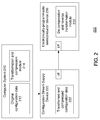
FIG. 2 is a block diagram of components of a system for electronically-configuring a programmable logic device in accordance with an embodiment of the invention. -
FIG. 3 is a flow chart of an exemplary method of transforming and compressing a data stream for electronically configuring a programmable logic device in accordance with an embodiment of the invention. -
FIG. 4 shows an exemplary block structure of configuration data for core resources in accordance with an embodiment of the invention. -
FIG. 5 illustrates an exemplary block-fingerprint library based on the block structure inFIG. 4 in accordance with an embodiment of the invention. -
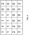
FIG. 6 depicts an exemplary block-bitmap representation of the configuration data for the block structure inFIG. 4 in accordance with an embodiment of the invention. -
FIG. 7 depicts the blocks of the core configuration data to which intra-block transformation is applied, and those to which intra-block transformation is applied, in accordance with an embodiment of the invention. -
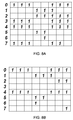
FIGS. 8A and 8B depict an exemplary block of configuration data before and after intra-block transformation, respectively, in accordance with an embodiment of the invention. -
FIG. 9 is a flow chart of an exemplary method of decompressing and reverse transforming a data stream by an electronically-programmable semiconductor device in accordance with an embodiment of the invention. - Complex FPGA devices use substantial amounts of configuration data to program all the user-desired functionality into the particular silicon device. This data set, commonly referred as bit-stream for historical reasons, is actually used to configure and program the multiple resources of the FPGA-hardware at the gate-level. As the sheer size of this data set keeps growing with each new generation of programmable devices, it is becoming a factor imposing usability limitations to the FPGA devices, not only because the increasing demands of non-volatile memory required to store this data; but also because the additional time demanded to read the configuration data onto the FPGA device, contributing to higher configuration times.
- Configuration data characterizes itself by presenting long sequences of zeroes, normally corresponding to unused hardware resources within the device. Previous approaches have exploited this type of redundancy. Altera Corporation of San Jose, California, for example, has used a compression method which replaces each null-nibble (equal to 0000) by a "0" in a preceding control word; while a not null-nibble is represented by a "1", trailed by the actual nibble value. The compression rate of this approach is bounded to a theoretical maximum of four times. In accordance with the present disclosure, such a compression method is an example of a one-dimensional (1D) compression method because it does not require information as to the two-dimensional block structure of the circuitry in the integrated circuit.
- The present disclosure provides an innovative approach to compressing and decompressing configuration data. The presently-disclosed approach takes advantage of the bit-oriented two-dimensional block structure of an FPGA core to provide increased compression ratios for real FPGA designs. The presently-disclosed approach may also be applied to other similarly structured electronically-programmable semiconductor devices.
-
FIG. 1 is a simplified partial block diagram of an exemplary electronically-programmable semiconductor that may be electronically-configured in accordance with an embodiment of the present invention. In this case, the exemplary programmable device is a field programmable gate array (FPGA) 1. It should be understood that embodiments of the present invention can be used in numerous types of integrated circuits such as field programmable gate arrays (FPGAs), programmable logic devices (PLDs), complex programmable logic devices (CPLDs), programmable logic arrays (PLAs), and other electronically-programmable semiconductor devices. -
FPGA 1 includes within its "core" a two-dimensional array of programmable logic array blocks (or LABs) 2 that are interconnected by a network of column and row interconnect conductors of varying length and speed.LABs 2 include multiple (e.g., ten) logic elements (or LEs). - An LE is a programmable logic block that provides for efficient implementation of user defined logic functions. An FPGA has numerous logic elements that can be configured to implement various combinatorial and sequential functions. The logic elements have access to a programmable interconnect structure. The programmable interconnect structure can be programmed to interconnect the logic elements in almost any desired configuration.
-
FPGA 1 may also include a distributed memory structure including random access memory (RAM) blocks of varying sizes provided throughout the array. The RAM blocks include, for example,blocks 4, andblocks 6. These memory blocks can also include shift registers and FIFO buffers. -
FPGA 1 may further include digital signal processing (DSP) blocks that can implement, for example, multipliers with add or subtract features. Input/output elements (IOEs) 12 located, in this example, around the periphery of the chip support numerous single-ended and differential input/output standards. EachIOE 12 is coupled to an external terminal (i.e., a pin) ofFPGA 10. -
FIG. 2 is a block diagram of components of a system for electronic configuration of an electronically-programmable semiconductor device in accordance with an embodiment of the invention. As shown, thesystem 200 may include an electronically-programmable semiconductor device 230, a configurationstream supply device 220 and acomputer system 210. - The
computer system 210 may includeoriginal configuration data 212 for configuring the semiconductor device 230. In addition, thecomputer system 210 may include a transformation and compression module 214. The transformation and compression module 214 may be executed by a processor of thecomputer system 210 so as to transform and compress theoriginal configuration data 212. The transformation and compression may involve 2D transformation (also referred to herein as 2D compression) followed by 1D compression, as described in the present disclosure. - The final
compressed configuration data 222 may be sent from thecomputer system 210 to the configurationstream supply device 220 in sequential form as a data stream. Hence, in the present disclosure, the configuration data sequence is frequently referred to as a configuration data-stream. - The configuration
stream supply device 220 may be, for example, a microcontroller which uses an embedded program to configure the semiconductor device 230, or a boot PROM which may be used to configure the semiconductor device 230 automatically upon power up. In a development environment, the configurationstream supply device 220 may be the computer system 210 (i.e. a separate configurationstream supply device 220 may not be needed). - The final
compressed configuration data 222 may be streamed from the configurationstream supply device 220 to the electronically-programmable semiconductor device 230. For example, the electronically-programmable semiconductor device 230 may be an FPGA or similar device. Advantageously, the finalcompressed configuration data 222 may be substantially smaller in size than theoriginal configuration data 212. - Within the electronically-programmable semiconductor device 230, the decompression and
reverse transformation module 232 may be used to de-compress and reverse transform the finalcompressed configuration data 222 to obtain theoriginal configuration data 212. The decompression and reverse transformation may involve 1D decompression and 2D reverse transformation (also referred to herein and 2D decompression). Theoriginal configuration data 212 may then be utilized to electronically configure the semiconductor device 230. -
FIG. 3 is a flow chart of anexemplary method 300 of transforming and compressing a data stream for electronically configuring a programmable logic device in accordance with an embodiment of the invention. Themethod 300 may be performed, for example, by the transformation and compression module 214 ofFIG. 2 . - Per block 302, configuration data for configuring an electronically-programmable semiconductor device may be obtained. For example, the configuration data may be the
original configuration data 212 ofFIG. 2 . - Configuration data in modern FPGAs comprises multiple data-segments, as a result of the complexity of these devices. A typical configuration data file includes segments related to peripheral resources (for example, input-output circuits, high-speed transceivers, and so on) and segments describing the configuration of a two-dimensional (2D) array of core resources.
- Per
step 304, segments of the configuration data related to the 2D array of core resources may be obtained. As described below, themethod 300 transforms these core segments before application of 1D compression. - Per
step 306, the 2D block structure for the 2D array of core resources is determined. Such a 2D block structure may be referred to herein as the "Block Descriptor" or "BD". - An exemplary 2D block structure for core resources is shown in
FIG. 4 . As depicted inFIG. 4 , the blocks may be of multiple types, such as, for example: block type A (including blocks A0, A1, A2, A4 and A5), block type B (including blocks B0, B1, B2, B3, B4 and B5), and block type C (including blocks C0, C1, C2, C3, C4 and C5). - Note that the block definition may be selected so that the different block types may have different widths (as shown in
FIG. 4 ) or so that the different block types share the same width (not shown). In the latter case, the columns of the 2D block structure would be of uniform width. In either case, the block definition (BD) is described in a compact form that is sent to, or already known by, the decompression andreverse transformation module 232. - The sequence of
steps including steps 308 through 312 may be performed for each block type in the BD. Perstep 308, a block type may be selected. For example, block type A may be first selected, and then later block types B and C may be selected. - Per
step 309, "fingerprints" (bitmaps) of blocks of the selected type are compared, and blocks with the same (or nearly the same) fingerprint are grouped together (i.e. designated as being the "same" block). One clear example of a block fingerprint that may appear repeatedly is that of a block representing a default un-used state of an FPGA IP-resource block type. - In one embodiment, only blocks with identical fingerprints (bitmaps) are considered to be the "same" block and so grouped together. For example, in
FIG. 4 , the three blocks A0 may have bitmaps that are identical. - In another embodiment, blocks with very similar, but slightly different, fingerprints (i.e. "sibling" blocks) may also be grouped together as having the "same" fingerprint. For example, in
FIG. 4 , the three blocks A0 may be siblings, rather than being strictly identical. In that case, the small difference between the siblings (delta data) may also be determined and stored. For example, if only one or a few bits (or bytes) are different between two blocks, the delta data for the second (sibling) block may include the locations of those bits (or bytes) that are different compared with the first block. - Per
step 310, an appearance count may be determined for each block fingerprint (including siblings, if applicable) within the set of blocks of the selected block type. For example, inFIG. 4 , for block type A, the appearance count for block A0 is 3, for block A1 is 2, for block A2 is 1, for block A4 is 1, and for block A5 is 1. - Per
step 312, the block fingerprints are ranked in descending order of appearance count, with the most frequently appearing ranking first. For example, inFIG. 4 , for block type A, the ranking would be first (rank=1) block A0, second (rank=2) block A1, third (rank=3) block A2, fourth (rank=4) block A4 and fifth (rank=5) block A5 . Note that blocks A2, A4 and A5, each have an appearance count of one, so the ranking between them may be determined to be in a predetermined order (for example, by an order of appearance). - Per
step 314, a determination may be made as to whether more block types in the BD are to be processed. If more block types are to be processed, then themethod 300 may loop back to step 308 where a next block type is selected. - If all the block types have been processed, then the
method 300 may move forward to the subsequent steps involving inter-block and intra-block transformations. As described below, inter-block transformation (steps 316 and 318) may be used to create a block-fingerprint library (BFL) and a 2D block bit map (BBM) so as to remove the data (step 320) for the (M-1) most-commonly-used block bitmaps of each block type. Furthermore, intra-block transformation (step 322) may be applied within the bitmaps of the remaining blocks not removed by the inter-block transformation. - Per step 316, a Block-Fingerprint Library (BFL) may be created. The BFL includes fingerprints of (M-1) most-commonly-used block bitmaps for each block type. In an exemplary implementation, the number M may be a power of two, such as 4, 8, 16, and so on. If siblings were grouped together, then the delta data for those (M-1) most-commonly-used block bitmaps may also be included in the BFL.
- For example, consider M = 4, such that the BFL includes fingerprints (bitmaps) of the three (4 - 1 = 3) most-commonly-used block bitmaps of each block type. The content of such a BFL is shown by the table in
FIG. 5 . As shown inFIG. 5 , the three most-commonly used block fingerprints are A0, A1, and A2 for block type A, B0, B1, and B2 for block type B, and C0, C1, and C2 for block type C. - Per
step 318, a 2D block bit map (BBM) may be created. In one implementation, the BBM associates an identifying digital number having log2 M bits with each block. For example, with M = 4, a two-bit digital number may be associated with each block via the BBM. - An example of such a BBM is provided in
FIG. 6 . As shown, the columns and rows in the BBM ofFIG. 6 correspond to the columns and rows, respectively, in the 2D block structure ofFIG. 4 . ComparingFIGS. 4 and6 shows that blocks A0, B0 and C0 inFIG. 4 have the identifying digital number 1 (binary 01) associated therewith inFIG. 6 due to their first ranking, blocks A1, B1 and C1 inFIG. 4 have the identifying digital number 2 (binary 10) associated therewith inFIG. 6 due to their second ranking, and blocks A2, B2 and C2 inFIG. 4 have the identifying digital number 3 (binary 11) associated therewith inFIG. 6 due to their third ranking. The remaining blocks inFIG. 4 have the identifying digital number 0 (binary 00) associated therewith inFIG. 6 to indicate that there is no fingerprint in the BFL associated therewith. - Per
step 320, the data for blocks represented in the BFL may then be removed from the configuration data sequence. Intra-block transformation may be applied to the remaining blocks in the configuration data sequence.FIG. 7 depicts the blocks of the core configuration data to which intra-block transformation is applied in accordance with an embodiment of the invention. In the example described above, inter-block transformation is applied to the shaded blocks (A0, A1, A2, B0, B1, B2, C0, C1 and C2) and is not applied to the remaining (unshaded) blocks (A4, A5, B3, B4, B5, C3, C4 and C5). - Per
step 322, an intra-block transformation may be applied within the bitmap of the blocks themselves to capture types of redundancy not captured with the inter-block transformation. In one implementation, the intra-block transformation is applied to blocks that are not represented within the BFL. In accordance with an embodiment of the invention, the intra-block transformation may utilize a bit-wise prediction of the configuration data based on adjacent bits inside the same block. - Complex silicon devices, such as FPGAs, generally use regular and repeatable design sub-block structures to generate complex design blocks. The size of these structures change from block-type to block-type, creating a singular pattern distance, for each block-type, in each of the x-y coordinates (for bits within a block). The compression algorithm described herein creates a prediction function Fk, where k is the total number of block types, which provides the bit-wise prediction for each
block type - According to an embodiment of the present invention, the 2D intra-block transformation replaces the actual configuration bits within a block with a bit-result reflecting one of the two following situations: i) a 0-bit is delivered to the output if the actual configuration bit matches with the prediction made for that configuration position; and ii) a 1-bit is delivered to the output if the actual configuration bit does not match with the prediction made for that configuration position. This functionality may be achieved by using the following exemplary bit-operation: bx,y = cx,y XOR Fk(x,y), where bx,y is the intra-sector transformed bit, cx,y is the original configuration bit from location (x,y), Fk(x,y) is the prediction function (of the
block types -
FIG. 8A depicts an exemplary block of configuration data before an intra-block transformation in accordance with an embodiment of the invention. Bits that have a value of one are shown as "1", and bits that have a value of zero are shown as blank. In this case, the prediction function Fk is used in which the pattern distance is four rows, such that each instance of the predictive pattern operates within four rows. - In this particular example, a first instance of the pattern is applied to
Rows 0 to 3, and a second instance of the pattern is applied toRows 4 to 7. Within the first instance,Row 0 is used to predictRow 3, andRow 1 is used to predict Row 2 (i.e. R0→R3 and R1→R2). Similarly, within the second instance,Row 4 is used to predictRow 7, andRow 5 is used to predict Row 6 (i.e. R4→R7 and R5→R6). Note that the above-discussed pattern is a relatively simple example of a predictive pattern that may be used. Other embodiments may use different predictive patterns. - The resulting bitmap after the intra-block transformation is shown in
FIG. 8B . The bits inRows FIG. 8B (the intra-transformed bitmap) are the same as the corresponding rows inFIG. 8A (the bitmap before intra-transformation) because those rows are used to predict bits in other rows (Rows -
Row 3 ofFIG. 8B includes only zero value bits because each bit value inRow 3 ofFIG. 8A is the same as the corresponding bit value inRow 0 ofFIG. 8A .Row 2 ofFIG. 8B includes zero value bits in the first six columns and one value bits in the last two columns, because only the last two columns inRows FIG. 8A differ from each other. -
Row 7 ofFIG. 8B includes zero value bits in the first seven columns and a one value bit in the last column, because only the last column inRows FIG. 8A differ from each other.Row 6 ofFIG. 8B includes one value bits only in the fourth column, because only the fourth column inRows FIG. 8A have bit values that differ from each other. - In accordance with an embodiment of the invention, the pattern distance may be selected for each block type such that statistically good predictions can be made, so as to result in better compression rates. Note that the decompressor, in order to restore the original configuration bit, makes the same bit-wise prediction using the selected pattern distance for each block type and applies an XOR operation between its own prediction and the incoming bit. Note, further, that the procedure described above may be performed byte-wise or word-wise for efficiency of implementation.
- In
step 322, the intra-block transformation may be applied to all the remaining blocks in the data-stream (those blocks that were not removed in step 320). The resultant data-stream may be referred to as the 2D-transformed (post-transformation) data-stream. The 2D-transformed data-stream includes the BFL created in step 316, the BBM created instep 318, delta data for sibling blocks (if any), required information for the prediction function Fk (for example, selected pattern distances), and the intra-block transformed bitmaps perstep 322. In addition, the 2D-transformed data-stream includes other configuration data needed to configure the electronically-programmable semiconductor device, such as configuration data for peripheral (non-core) circuits. - Per
step 324, after the blocks of configuration data have been filtered by both types of 2D transformations, the resultant 2D-transformed data-stream may be further compressed using a 1D-compression procedure so as to obtain a final compressed data-stream. In an exemplary implementation, a Lempel-Ziv (LZ) type of 1D compression procedure may be used advantageously. In one implementation, the 1D compression is not applied to the BFL and the BBM, although the 1D compression may be applied to the BFL and the BBM in an alternate implementation. - In summary, the above-described compression technique applies both inter-block 2D compression and intra-block 2D compression to provide the combined effect of reducing the net size of the data source, as well as providing an increased amount of redundancy in the transformed data. Thereafter, 1D compression is advantageously applied to generate a final compressed data-stream that is substantially smaller than a compressed data-stream using 1D compression alone.
- Finally, per
step 326, the final compressed data-stream is sent to the electronically-programmable semiconductor device 230. In one embodiment, prior to being transmitted, the 1D-compressed post-transformation data-stream 222 may be sent to, and stored in, a configurationstream supply device 220, such as illustrated inFIG. 2 . The configurationstream supply device 220 may then transmit the final compressed data-stream to the electronically-programmable semiconductor device 230. As described further below, a decompression andreverse transformation module 232 in the electronically-programmable semiconductor device 230 decompresses and reverse transforms the data-stream so that the original data-stream may be used to electronically configure the circuits within the semiconductor device 230. -
FIG. 9 is a flow chart of anexemplary method 900 of decompressing and reverse transforming a data stream by an electronically-programmable semiconductor device in accordance with an embodiment of the invention. Themethod 900 may be performed, for example, by the decompression and reverse transformation andcompression module 232 ofFIG. 2 . - Per
step 902, the final compressed post-transformation data-stream is received by the semiconductor device. In one embodiment, the final compressed post-transformation data-stream is received by the semiconductor device 230 from the configurationstream supply device 220. - Per
step compression procedure 300. As described above, the 1D-decompressed data-stream includes the BFL, the BBM, delta data for sibling blocks (if any), required information for the prediction function Fk (for example, selected pattern distances), and the intra-block transformed bitmaps. In addition, the 1D-decompressed data-stream includes other configuration data needed to configure the electronically-programmable semiconductor device, such as configuration data for peripheral (non-core) circuits. - Next, the 2D reverse transformation (2D decompression) may be applied to the 1D-decompressed data-stream. The 2D reverse transformation includes both the Inter-block and Intra-block reverse transformations. Note that the algorithm described herein does not strictly require sequential decompression of Inter-block and Intra-block reverse transformations. Such ordering is valid for the transformations performed by the compressor, because of the priority of full-matching blocks, but not for the reverse transformations performed by the decompressor. In fact, during decompression, the Intra-block reverse transformation (step 906) and the Inter-Sector reverse transformation (step 908) may be performed in parallel.
- Per
step 906, the prediction function Fk is used to reverse the intra-block transformation of the blocks that was done by the transformation and compression module 214 so as to obtain the original blocks. Note that, in one implementation, since the intra-block transformation by the compressor and the reverse intra-block transformation by the decompressor are not applied to the blocks represented within the BFL; they are applied only to the blocks not represented within the BFL. In the example intra-block transformation described above in relation toFIGS. 8A and 8B , the original configuration bit may be regenerated by applying an XOR operation to the intra-block transformed and predicted bits. In other words, cx,y = bx,y XOR Fk(x,y). - Per
step 908, which may be performed in parallel to step 906, the BBM, BFL, and the delta data for siblings (if applicable) are extracted and used to reverse the inter-block transformation. The BBM is used as a guide to determine which blocks are to be copied from the BFL to positions in the data-stream indicated by the BBM, and the delta data is applied to make the adjustments to re-create the sibling blocks, if applicable. - As a result of
steps step 910. The original data-stream may then be used to electronically configure the semiconductor device 230 perstep 912. -
-
Embodiment 1. A method for decompressing a data-stream to regenerate an original data-stream of configuration data for electronically configuring an electronically-programmable semiconductor device which includes a two-dimensional block structure for an array of core resources of the electronically-programmable semiconductor device, wherein the two dimensional block structure includes a plurality of block types, and wherein blocks belonging to a same block type have a same width and a same length in bits, the method being performed by a decompression and reverse transformation module in the electronically-programmable semiconductor device and comprising:- receiving the data-stream from a configuration stream supply device;
- extracting a block fingerprint library and a block bit map from the data-stream; and
- inserting copies of blocks from the block fingerprint library as identified by the block bit map into the data-stream at positions indicated by the block bit map.
-
Embodiment 2. The method ofEmbodiment 1, wherein the block fingerprint library includes a plurality of most-commonly-used block fingerprints for each of the plurality of block types. -
Embodiment 3. The method ofEmbodiment 2, wherein the block bit map associates a plurality of bits with each block of the two-dimensional block structure, wherein the plurality of bits indicates which of the plurality of most-commonly-used block fingerprints, if any, is associated with said block. -
Embodiment 4. The method ofEmbodiment - reversing intra-block transformation of remaining blocks in the data stream that are not in the block fingerprint library using an inverse prediction function.
-
Embodiment 5. The method ofEmbodiment 4, wherein the inverse prediction function depends on a plurality of pattern distances corresponding to the plurality of block types. -
Embodiment 6. The method ofEmbodiment - applying one-dimensional decompression to the remaining blocks, wherein the one-dimensional decompression does not require information of the two-dimensional block structure.
-
Embodiment 7. A semiconductor device comprising:- an array of core resources having a two-dimensional block structure;
- a decompression and reverse transformation module that regenerates an original data-stream of configuration data by performing steps including:
- receiving a data-stream from a configuration stream supply device;
- performing a one-dimensional decompression on a portion of the data-stream, wherein the one-dimensional decompression does not require information of the two-dimensional block structure; and
- performing a reverse intra-block transformation on said portion of the data-stream.
- Embodiment 8. The semiconductor device of
Embodiment 7, wherein the steps performed by the decompression and reverse transformation module further include: performing a reverse inter-block transformation by extracting a block fingerprint library and a block bit map from the data-stream, and inserting copies of blocks from the block fingerprint library as identified by the block bit map into the data-stream at positions indicated by the block bit map. - Embodiment 9. The semiconductor device of Embodiment 8, wherein the reverse intra-block transformation and the reverse inter-block transformation are performed in parallel.
- In the above description, numerous specific details are given to provide a thorough understanding of embodiments of the invention. However, the above description of illustrated embodiments of the invention is not intended to be exhaustive or to limit the invention to the precise forms disclosed. One skilled in the relevant art will recognize that the invention can be practiced without one or more of the specific details, or with other methods, components, etc.
- In other instances, well-known structures or operations are not shown or described in detail to avoid obscuring aspects of the invention. While specific embodiments of, and examples for, the invention are described herein for illustrative purposes, various equivalent modifications are possible within the scope of the invention, as those skilled in the relevant art will recognize. These modifications may be made to the invention in light of the above detailed description.
Claims (12)
- A method for compressing a data-stream of configuration data for electronically configuring an electronically-programmable semiconductor device (230), the method (300) being performed by a transformation and compression module (214) and comprising:determining (306) a two-dimensional block structure for an array of core resources of the electronically-programmable semiconductor device (230), wherein the two-dimensional block structure includes a plurality of block types, and wherein blocks belonging to a same block type have a same width and a same length in bits, and wherein each block has a block fingerprint corresponding to content of the block;determining (310, 312) a plurality of most-commonly-used block fingerprints for each block type of the plurality of block types; andcreating (316) a block fingerprint library that includes the plurality of most-commonly-used block fingerprints for each block type.
- The method of claim 1, further comprising:removing (320) from the data-stream blocks which are expressed by any one of the plurality of most-commonly-used block fingerprints for the plurality of block types; andinserting the block fingerprint library into the data-stream at a position before the removed blocks.
- The method of claim 2, further comprising:creating (318) a block bit map that associates a plurality of bits with each block of the two-dimensional block structure, wherein the plurality of bits indicates which of the plurality of most-commonly-used block fingerprints, if any, is associated with said block; andinserting a block descriptor and the block bit map into the data-stream at a position before the removed blocks.
- The method of claim 3, further comprising:applying (322) an intra-block transform to blocks remaining in the data-stream using a prediction function.
- The method of claim 4, wherein the prediction function depends on a plurality of pattern distances corresponding to the plurality of block types.
- The method of claim 4 or 5, further comprising:applying (324) a one-dimensional compression to the data-stream after application of the intra-block transform, wherein the one-dimensional compression does not require information of the two-dimensional block structure.
- A system for compressing a data-stream of configuration data for electronically configuring an electronically-programmable semiconductor device (230), the system comprising:a transformation and compression module (214) that generates a transformed and compressed data-stream by performing steps including:determining (306) a two-dimensional block structure for a two-dimensional array of core resources of the semiconductor device (230), wherein the two-dimensional block structure includes a plurality of block types, and wherein blocks belonging to a same block type have a same width and a same length in bits, and wherein each block has a block fingerprint corresponding to content of the block;determining (310, 312) a plurality of most-commonly-used block fingerprints for each block type; andcreating (316) a block fingerprint library that includes the plurality of most-commonly-used block fingerprints for each block type; anda configuration stream supply device (220) that transmits the transformed and compressed data-stream to the electronically-programmable semiconductor device (230).
- The system of claim 7, wherein the steps performed by the transformation and compression module (214) further include:removing (320) from the data-stream blocks which are expressed by any one of the plurality of most-commonly-used block fingerprints for the plurality of block types; andinserting the block fingerprint library into the data-stream at a position before the removed blocks.
- The system of claim 8, wherein the steps performed by the transformation and compression module (214) further include:creating (318) a block bit map that associates a plurality of bits with each block of the two-dimensional block structure, wherein the plurality of bits indicates which of the plurality of most-commonly-used block fingerprints, if any, is associated with said block; andinserting a block descriptor and the block bit map into the data-stream at a position before the removed blocks.
- The system of claim 9, wherein the steps performed by the transformation and compression module (214) further include:applying (322) an intra-block transform to blocks remaining in the data-stream using a prediction function.
- The system of claim 10, wherein the prediction function depends on a plurality of pattern distances corresponding to the plurality of block types.
- The system of claim 10 or 11, wherein the steps performed by the transformation and compression module (214) further include:applying (324) a one-dimensional compression to the data-stream after application of the intra-block transform, wherein the one-dimensional compression does not require information of the two-dimensional block structure.
Applications Claiming Priority (1)
| Application Number | Priority Date | Filing Date | Title |
|---|---|---|---|
| US14/634,757 US20160253096A1 (en) | 2015-02-28 | 2015-02-28 | Methods and apparatus for two-dimensional block bit-stream compression and decompression |
Publications (2)
| Publication Number | Publication Date |
|---|---|
| EP3065300A1 true EP3065300A1 (en) | 2016-09-07 |
| EP3065300B1 EP3065300B1 (en) | 2018-01-24 |
Family
ID=55456597
Family Applications (1)
| Application Number | Title | Priority Date | Filing Date |
|---|---|---|---|
| EP16156956.1A Active EP3065300B1 (en) | 2015-02-28 | 2016-02-23 | Methods and apparatus for two-dimensional block bit-stream compression and decompression |
Country Status (3)
| Country | Link |
|---|---|
| US (1) | US20160253096A1 (en) |
| EP (1) | EP3065300B1 (en) |
| CN (1) | CN105931278B (en) |
Cited By (1)
| Publication number | Priority date | Publication date | Assignee | Title |
|---|---|---|---|---|
| US10560102B1 (en) | 2016-11-17 | 2020-02-11 | Google Llc | Field programmable gate array including coupled lookup tables |
Families Citing this family (1)
| Publication number | Priority date | Publication date | Assignee | Title |
|---|---|---|---|---|
| US10972569B2 (en) * | 2017-04-24 | 2021-04-06 | International Business Machines Corporation | Apparatus, method, and computer program product for heterogenous compression of data streams |
Citations (3)
| Publication number | Priority date | Publication date | Assignee | Title |
|---|---|---|---|---|
| US6205574B1 (en) * | 1998-07-28 | 2001-03-20 | Xilinx, Inc. | Method and system for generating a programming bitstream including identification bits |
| US6327634B1 (en) * | 1998-08-25 | 2001-12-04 | Xilinx, Inc. | System and method for compressing and decompressing configuration data for an FPGA |
| US7902865B1 (en) * | 2007-11-15 | 2011-03-08 | Lattice Semiconductor Corporation | Compression and decompression of configuration data using repeated data frames |
Family Cites Families (9)
| Publication number | Priority date | Publication date | Assignee | Title |
|---|---|---|---|---|
| US6341178B1 (en) * | 1995-12-04 | 2002-01-22 | Xerox Corporation | Method and apparatus for lossless precompression of binary images |
| US6525678B1 (en) * | 2000-10-06 | 2003-02-25 | Altera Corporation | Configuring a programmable logic device |
| CN101882439B (en) * | 2010-06-10 | 2012-02-08 | 复旦大学 | A Compressed Domain Audio Fingerprint Method Based on Zernike Moments |
| CN102722583A (en) * | 2012-06-07 | 2012-10-10 | 无锡众志和达存储技术有限公司 | Hardware accelerating device for data de-duplication and method |
| CN102833546B (en) * | 2012-08-21 | 2015-03-04 | 中国科学院光电技术研究所 | High-speed image compression method and device based on wavelet sub-band interleaving optimal quantization |
| CN102831222B (en) * | 2012-08-24 | 2014-12-31 | 华中科技大学 | Differential compression method based on data de-duplication |
| CN103870514B (en) * | 2012-12-18 | 2018-03-09 | 华为技术有限公司 | Data de-duplication method and device |
| CN103177111B (en) * | 2013-03-29 | 2016-02-24 | 西安理工大学 | Data deduplication system and delet method thereof |
| CN103220226B (en) * | 2013-05-02 | 2016-04-20 | 百度在线网络技术(北京)有限公司 | Transparent real-time traffic compression method and system between data center |
-
2015
- 2015-02-28 US US14/634,757 patent/US20160253096A1/en not_active Abandoned
-
2016
- 2016-02-23 EP EP16156956.1A patent/EP3065300B1/en active Active
- 2016-02-26 CN CN201610109226.4A patent/CN105931278B/en active Active
Patent Citations (3)
| Publication number | Priority date | Publication date | Assignee | Title |
|---|---|---|---|---|
| US6205574B1 (en) * | 1998-07-28 | 2001-03-20 | Xilinx, Inc. | Method and system for generating a programming bitstream including identification bits |
| US6327634B1 (en) * | 1998-08-25 | 2001-12-04 | Xilinx, Inc. | System and method for compressing and decompressing configuration data for an FPGA |
| US7902865B1 (en) * | 2007-11-15 | 2011-03-08 | Lattice Semiconductor Corporation | Compression and decompression of configuration data using repeated data frames |
Cited By (2)
| Publication number | Priority date | Publication date | Assignee | Title |
|---|---|---|---|---|
| US10560102B1 (en) | 2016-11-17 | 2020-02-11 | Google Llc | Field programmable gate array including coupled lookup tables |
| US10868539B1 (en) | 2016-11-17 | 2020-12-15 | Google Llc | Field programmable gate array including coupled lookup tables |
Also Published As
| Publication number | Publication date |
|---|---|
| CN105931278A (en) | 2016-09-07 |
| EP3065300B1 (en) | 2018-01-24 |
| CN105931278B (en) | 2020-02-28 |
| US20160253096A1 (en) | 2016-09-01 |
Similar Documents
| Publication | Publication Date | Title |
|---|---|---|
| EP3661061A1 (en) | Data compression and storage | |
| US8058898B1 (en) | Compression and decompression of configuration data using repeated data frames | |
| CN106484942B (en) | Efficient integrated circuit configuration data management | |
| KR102467816B1 (en) | Extension of the mpeg/sc3dmc standard to polygon meshes | |
| US6327634B1 (en) | System and method for compressing and decompressing configuration data for an FPGA | |
| Kumar et al. | Low‐latency median filter core for hardware implementation of 5× 5 median filtering | |
| JP4443165B2 (en) | Image compression apparatus and image compression method | |
| EP3065300B1 (en) | Methods and apparatus for two-dimensional block bit-stream compression and decompression | |
| Li | Configuration management techniques for reconfigurable computing | |
| EP3082107B1 (en) | Image synthesis | |
| US7446679B1 (en) | Compression and decompression of configuration data for programmable logic devices | |
| CN102323541A (en) | Test method for SOC (System On Chip) based on reference vector and bit mask | |
| JP3675255B2 (en) | Information processing device | |
| EP4116924A1 (en) | Mapping multi-dimensional coordinates to a 1d space | |
| US20120092987A1 (en) | Routing apparatus and network apparatus | |
| CN109255771B (en) | Image filtering method and device | |
| Sierra et al. | High-performance decoding of variable-length memory data packets for FPGA stream processing | |
| CN119093943B (en) | System, device, method and integrated circuit chip for parallel extraction of compressed data | |
| KR100396237B1 (en) | The method and apparatus for iterative over-approximate reachable state computation | |
| JP2004056417A (en) | Decoder and decoding method | |
| US10402111B1 (en) | Systems and methods for data storage compression | |
| Mohey et al. | Design and implementation of Lempel-Ziv data compression using FPGA | |
| CN120811374A (en) | Data acquisition method and data acquisition card | |
| Amer et al. | A design flow for an H. 264 embedded video encoder | |
| Carter et al. | Architecture for dynamically reconfigurable real-time lossless compression |
Legal Events
| Date | Code | Title | Description |
|---|---|---|---|
| PUAI | Public reference made under article 153(3) epc to a published international application that has entered the european phase |
Free format text: ORIGINAL CODE: 0009012 |
|
| AK | Designated contracting states |
Kind code of ref document: A1 Designated state(s): AL AT BE BG CH CY CZ DE DK EE ES FI FR GB GR HR HU IE IS IT LI LT LU LV MC MK MT NL NO PL PT RO RS SE SI SK SM TR |
|
| AX | Request for extension of the european patent |
Extension state: BA ME |
|
| STAA | Information on the status of an ep patent application or granted ep patent |
Free format text: STATUS: REQUEST FOR EXAMINATION WAS MADE |
|
| 17P | Request for examination filed |
Effective date: 20170202 |
|
| RBV | Designated contracting states (corrected) |
Designated state(s): AL AT BE BG CH CY CZ DE DK EE ES FI FR GB GR HR HU IE IS IT LI LT LU LV MC MK MT NL NO PL PT RO RS SE SI SK SM TR |
|
| REG | Reference to a national code |
Ref country code: DE Ref legal event code: R079 Ref document number: 602016001415 Country of ref document: DE Free format text: PREVIOUS MAIN CLASS: H03K0019177000 Ipc: G06F0003060000 |
|
| RIC1 | Information provided on ipc code assigned before grant |
Ipc: G06F 3/06 20060101AFI20170714BHEP |
|
| GRAP | Despatch of communication of intention to grant a patent |
Free format text: ORIGINAL CODE: EPIDOSNIGR1 |
|
| STAA | Information on the status of an ep patent application or granted ep patent |
Free format text: STATUS: GRANT OF PATENT IS INTENDED |
|
| INTG | Intention to grant announced |
Effective date: 20170904 |
|
| GRAS | Grant fee paid |
Free format text: ORIGINAL CODE: EPIDOSNIGR3 |
|
| GRAA | (expected) grant |
Free format text: ORIGINAL CODE: 0009210 |
|
| STAA | Information on the status of an ep patent application or granted ep patent |
Free format text: STATUS: THE PATENT HAS BEEN GRANTED |
|
| AK | Designated contracting states |
Kind code of ref document: B1 Designated state(s): AL AT BE BG CH CY CZ DE DK EE ES FI FR GB GR HR HU IE IS IT LI LT LU LV MC MK MT NL NO PL PT RO RS SE SI SK SM TR |
|
| REG | Reference to a national code |
Ref country code: GB Ref legal event code: FG4D |
|
| REG | Reference to a national code |
Ref country code: CH Ref legal event code: EP |
|
| REG | Reference to a national code |
Ref country code: AT Ref legal event code: REF Ref document number: 966132 Country of ref document: AT Kind code of ref document: T Effective date: 20180215 |
|
| REG | Reference to a national code |
Ref country code: IE Ref legal event code: FG4D |
|
| REG | Reference to a national code |
Ref country code: DE Ref legal event code: R096 Ref document number: 602016001415 Country of ref document: DE |
|
| REG | Reference to a national code |
Ref country code: FR Ref legal event code: PLFP Year of fee payment: 3 |
|
| REG | Reference to a national code |
Ref country code: NL Ref legal event code: MP Effective date: 20180124 |
|
| REG | Reference to a national code |
Ref country code: LT Ref legal event code: MG4D |
|
| REG | Reference to a national code |
Ref country code: AT Ref legal event code: MK05 Ref document number: 966132 Country of ref document: AT Kind code of ref document: T Effective date: 20180124 |
|
| PG25 | Lapsed in a contracting state [announced via postgrant information from national office to epo] |
Ref country code: NL Free format text: LAPSE BECAUSE OF FAILURE TO SUBMIT A TRANSLATION OF THE DESCRIPTION OR TO PAY THE FEE WITHIN THE PRESCRIBED TIME-LIMIT Effective date: 20180124 |
|
| PG25 | Lapsed in a contracting state [announced via postgrant information from national office to epo] |
Ref country code: ES Free format text: LAPSE BECAUSE OF FAILURE TO SUBMIT A TRANSLATION OF THE DESCRIPTION OR TO PAY THE FEE WITHIN THE PRESCRIBED TIME-LIMIT Effective date: 20180124 Ref country code: LT Free format text: LAPSE BECAUSE OF FAILURE TO SUBMIT A TRANSLATION OF THE DESCRIPTION OR TO PAY THE FEE WITHIN THE PRESCRIBED TIME-LIMIT Effective date: 20180124 Ref country code: HR Free format text: LAPSE BECAUSE OF FAILURE TO SUBMIT A TRANSLATION OF THE DESCRIPTION OR TO PAY THE FEE WITHIN THE PRESCRIBED TIME-LIMIT Effective date: 20180124 Ref country code: NO Free format text: LAPSE BECAUSE OF FAILURE TO SUBMIT A TRANSLATION OF THE DESCRIPTION OR TO PAY THE FEE WITHIN THE PRESCRIBED TIME-LIMIT Effective date: 20180424 Ref country code: FI Free format text: LAPSE BECAUSE OF FAILURE TO SUBMIT A TRANSLATION OF THE DESCRIPTION OR TO PAY THE FEE WITHIN THE PRESCRIBED TIME-LIMIT Effective date: 20180124 Ref country code: CY Free format text: LAPSE BECAUSE OF FAILURE TO SUBMIT A TRANSLATION OF THE DESCRIPTION OR TO PAY THE FEE WITHIN THE PRESCRIBED TIME-LIMIT Effective date: 20180124 |
|
| PG25 | Lapsed in a contracting state [announced via postgrant information from national office to epo] |
Ref country code: SE Free format text: LAPSE BECAUSE OF FAILURE TO SUBMIT A TRANSLATION OF THE DESCRIPTION OR TO PAY THE FEE WITHIN THE PRESCRIBED TIME-LIMIT Effective date: 20180124 Ref country code: IS Free format text: LAPSE BECAUSE OF FAILURE TO SUBMIT A TRANSLATION OF THE DESCRIPTION OR TO PAY THE FEE WITHIN THE PRESCRIBED TIME-LIMIT Effective date: 20180524 Ref country code: PL Free format text: LAPSE BECAUSE OF FAILURE TO SUBMIT A TRANSLATION OF THE DESCRIPTION OR TO PAY THE FEE WITHIN THE PRESCRIBED TIME-LIMIT Effective date: 20180124 Ref country code: LV Free format text: LAPSE BECAUSE OF FAILURE TO SUBMIT A TRANSLATION OF THE DESCRIPTION OR TO PAY THE FEE WITHIN THE PRESCRIBED TIME-LIMIT Effective date: 20180124 Ref country code: GR Free format text: LAPSE BECAUSE OF FAILURE TO SUBMIT A TRANSLATION OF THE DESCRIPTION OR TO PAY THE FEE WITHIN THE PRESCRIBED TIME-LIMIT Effective date: 20180425 Ref country code: BG Free format text: LAPSE BECAUSE OF FAILURE TO SUBMIT A TRANSLATION OF THE DESCRIPTION OR TO PAY THE FEE WITHIN THE PRESCRIBED TIME-LIMIT Effective date: 20180424 Ref country code: AT Free format text: LAPSE BECAUSE OF FAILURE TO SUBMIT A TRANSLATION OF THE DESCRIPTION OR TO PAY THE FEE WITHIN THE PRESCRIBED TIME-LIMIT Effective date: 20180124 Ref country code: RS Free format text: LAPSE BECAUSE OF FAILURE TO SUBMIT A TRANSLATION OF THE DESCRIPTION OR TO PAY THE FEE WITHIN THE PRESCRIBED TIME-LIMIT Effective date: 20180124 |
|
| REG | Reference to a national code |
Ref country code: DE Ref legal event code: R097 Ref document number: 602016001415 Country of ref document: DE |
|
| PG25 | Lapsed in a contracting state [announced via postgrant information from national office to epo] |
Ref country code: IT Free format text: LAPSE BECAUSE OF FAILURE TO SUBMIT A TRANSLATION OF THE DESCRIPTION OR TO PAY THE FEE WITHIN THE PRESCRIBED TIME-LIMIT Effective date: 20180124 Ref country code: RO Free format text: LAPSE BECAUSE OF FAILURE TO SUBMIT A TRANSLATION OF THE DESCRIPTION OR TO PAY THE FEE WITHIN THE PRESCRIBED TIME-LIMIT Effective date: 20180124 Ref country code: MC Free format text: LAPSE BECAUSE OF FAILURE TO SUBMIT A TRANSLATION OF THE DESCRIPTION OR TO PAY THE FEE WITHIN THE PRESCRIBED TIME-LIMIT Effective date: 20180124 Ref country code: AL Free format text: LAPSE BECAUSE OF FAILURE TO SUBMIT A TRANSLATION OF THE DESCRIPTION OR TO PAY THE FEE WITHIN THE PRESCRIBED TIME-LIMIT Effective date: 20180124 Ref country code: EE Free format text: LAPSE BECAUSE OF FAILURE TO SUBMIT A TRANSLATION OF THE DESCRIPTION OR TO PAY THE FEE WITHIN THE PRESCRIBED TIME-LIMIT Effective date: 20180124 |
|
| REG | Reference to a national code |
Ref country code: IE Ref legal event code: MM4A |
|
| REG | Reference to a national code |
Ref country code: BE Ref legal event code: MM Effective date: 20180228 |
|
| PG25 | Lapsed in a contracting state [announced via postgrant information from national office to epo] |
Ref country code: SM Free format text: LAPSE BECAUSE OF FAILURE TO SUBMIT A TRANSLATION OF THE DESCRIPTION OR TO PAY THE FEE WITHIN THE PRESCRIBED TIME-LIMIT Effective date: 20180124 Ref country code: LU Free format text: LAPSE BECAUSE OF NON-PAYMENT OF DUE FEES Effective date: 20180223 Ref country code: CZ Free format text: LAPSE BECAUSE OF FAILURE TO SUBMIT A TRANSLATION OF THE DESCRIPTION OR TO PAY THE FEE WITHIN THE PRESCRIBED TIME-LIMIT Effective date: 20180124 Ref country code: SK Free format text: LAPSE BECAUSE OF FAILURE TO SUBMIT A TRANSLATION OF THE DESCRIPTION OR TO PAY THE FEE WITHIN THE PRESCRIBED TIME-LIMIT Effective date: 20180124 Ref country code: DK Free format text: LAPSE BECAUSE OF FAILURE TO SUBMIT A TRANSLATION OF THE DESCRIPTION OR TO PAY THE FEE WITHIN THE PRESCRIBED TIME-LIMIT Effective date: 20180124 |
|
| PLBE | No opposition filed within time limit |
Free format text: ORIGINAL CODE: 0009261 |
|
| STAA | Information on the status of an ep patent application or granted ep patent |
Free format text: STATUS: NO OPPOSITION FILED WITHIN TIME LIMIT |
|
| 26N | No opposition filed |
Effective date: 20181025 |
|
| PG25 | Lapsed in a contracting state [announced via postgrant information from national office to epo] |
Ref country code: IE Free format text: LAPSE BECAUSE OF NON-PAYMENT OF DUE FEES Effective date: 20180223 |
|
| PG25 | Lapsed in a contracting state [announced via postgrant information from national office to epo] |
Ref country code: BE Free format text: LAPSE BECAUSE OF NON-PAYMENT OF DUE FEES Effective date: 20180228 Ref country code: SI Free format text: LAPSE BECAUSE OF FAILURE TO SUBMIT A TRANSLATION OF THE DESCRIPTION OR TO PAY THE FEE WITHIN THE PRESCRIBED TIME-LIMIT Effective date: 20180124 |
|
| REG | Reference to a national code |
Ref country code: CH Ref legal event code: PL |
|
| PG25 | Lapsed in a contracting state [announced via postgrant information from national office to epo] |
Ref country code: CH Free format text: LAPSE BECAUSE OF NON-PAYMENT OF DUE FEES Effective date: 20190228 Ref country code: LI Free format text: LAPSE BECAUSE OF NON-PAYMENT OF DUE FEES Effective date: 20190228 |
|
| PG25 | Lapsed in a contracting state [announced via postgrant information from national office to epo] |
Ref country code: MT Free format text: LAPSE BECAUSE OF NON-PAYMENT OF DUE FEES Effective date: 20180223 |
|
| PG25 | Lapsed in a contracting state [announced via postgrant information from national office to epo] |
Ref country code: TR Free format text: LAPSE BECAUSE OF FAILURE TO SUBMIT A TRANSLATION OF THE DESCRIPTION OR TO PAY THE FEE WITHIN THE PRESCRIBED TIME-LIMIT Effective date: 20180124 |
|
| PG25 | Lapsed in a contracting state [announced via postgrant information from national office to epo] |
Ref country code: PT Free format text: LAPSE BECAUSE OF FAILURE TO SUBMIT A TRANSLATION OF THE DESCRIPTION OR TO PAY THE FEE WITHIN THE PRESCRIBED TIME-LIMIT Effective date: 20180124 |
|
| PG25 | Lapsed in a contracting state [announced via postgrant information from national office to epo] |
Ref country code: MK Free format text: LAPSE BECAUSE OF NON-PAYMENT OF DUE FEES Effective date: 20180124 Ref country code: HU Free format text: LAPSE BECAUSE OF FAILURE TO SUBMIT A TRANSLATION OF THE DESCRIPTION OR TO PAY THE FEE WITHIN THE PRESCRIBED TIME-LIMIT; INVALID AB INITIO Effective date: 20160223 |
|
| GBPC | Gb: european patent ceased through non-payment of renewal fee |
Effective date: 20200223 |
|
| PG25 | Lapsed in a contracting state [announced via postgrant information from national office to epo] |
Ref country code: GB Free format text: LAPSE BECAUSE OF NON-PAYMENT OF DUE FEES Effective date: 20200223 |
|
| P01 | Opt-out of the competence of the unified patent court (upc) registered |
Effective date: 20230531 |
|
| PGFP | Annual fee paid to national office [announced via postgrant information from national office to epo] |
Ref country code: DE Payment date: 20260217 Year of fee payment: 11 |
|
| PGFP | Annual fee paid to national office [announced via postgrant information from national office to epo] |
Ref country code: FR Payment date: 20260219 Year of fee payment: 11 |