EP3063574B1 - Multiplexed optoelectronic engines - Google Patents
Multiplexed optoelectronic engines Download PDFInfo
- Publication number
- EP3063574B1 EP3063574B1 EP13896285.7A EP13896285A EP3063574B1 EP 3063574 B1 EP3063574 B1 EP 3063574B1 EP 13896285 A EP13896285 A EP 13896285A EP 3063574 B1 EP3063574 B1 EP 3063574B1
- Authority
- EP
- European Patent Office
- Prior art keywords
- wavelength
- light
- beams
- optical
- photodetector
- Prior art date
- Legal status (The legal status is an assumption and is not a legal conclusion. Google has not performed a legal analysis and makes no representation as to the accuracy of the status listed.)
- Active
Links
Images


Classifications
-
- G—PHYSICS
- G02—OPTICS
- G02B—OPTICAL ELEMENTS, SYSTEMS OR APPARATUS
- G02B6/00—Light guides; Structural details of arrangements comprising light guides and other optical elements, e.g. couplings
- G02B6/24—Coupling light guides
- G02B6/26—Optical coupling means
- G02B6/28—Optical coupling means having data bus means, i.e. plural waveguides interconnected and providing an inherently bidirectional system by mixing and splitting signals
- G02B6/293—Optical coupling means having data bus means, i.e. plural waveguides interconnected and providing an inherently bidirectional system by mixing and splitting signals with wavelength selective means
- G02B6/29346—Optical coupling means having data bus means, i.e. plural waveguides interconnected and providing an inherently bidirectional system by mixing and splitting signals with wavelength selective means operating by wave or beam interference
- G02B6/29361—Interference filters, e.g. multilayer coatings, thin film filters, dichroic splitters or mirrors based on multilayers, WDM filters
- G02B6/29362—Serial cascade of filters or filtering operations, e.g. for a large number of channels
- G02B6/29365—Serial cascade of filters or filtering operations, e.g. for a large number of channels in a multireflection configuration, i.e. beam following a zigzag path between filters or filtering operations
- G02B6/29367—Zigzag path within a transparent optical block, e.g. filter deposited on an etalon, glass plate, wedge acting as a stable spacer
-
- G—PHYSICS
- G02—OPTICS
- G02B—OPTICAL ELEMENTS, SYSTEMS OR APPARATUS
- G02B6/00—Light guides; Structural details of arrangements comprising light guides and other optical elements, e.g. couplings
- G02B6/24—Coupling light guides
- G02B6/26—Optical coupling means
- G02B6/28—Optical coupling means having data bus means, i.e. plural waveguides interconnected and providing an inherently bidirectional system by mixing and splitting signals
- G02B6/293—Optical coupling means having data bus means, i.e. plural waveguides interconnected and providing an inherently bidirectional system by mixing and splitting signals with wavelength selective means
- G02B6/29379—Optical coupling means having data bus means, i.e. plural waveguides interconnected and providing an inherently bidirectional system by mixing and splitting signals with wavelength selective means characterised by the function or use of the complete device
- G02B6/2938—Optical coupling means having data bus means, i.e. plural waveguides interconnected and providing an inherently bidirectional system by mixing and splitting signals with wavelength selective means characterised by the function or use of the complete device for multiplexing or demultiplexing, i.e. combining or separating wavelengths, e.g. 1xN, NxM
-
- G—PHYSICS
- G02—OPTICS
- G02B—OPTICAL ELEMENTS, SYSTEMS OR APPARATUS
- G02B6/00—Light guides; Structural details of arrangements comprising light guides and other optical elements, e.g. couplings
- G02B6/24—Coupling light guides
- G02B6/42—Coupling light guides with opto-electronic elements
- G02B6/4201—Packages, e.g. shape, construction, internal or external details
- G02B6/4204—Packages, e.g. shape, construction, internal or external details the coupling comprising intermediate optical elements, e.g. lenses, holograms
- G02B6/4215—Packages, e.g. shape, construction, internal or external details the coupling comprising intermediate optical elements, e.g. lenses, holograms the intermediate optical elements being wavelength selective optical elements, e.g. variable wavelength optical modules or wavelength lockers
-
- H—ELECTRICITY
- H04—ELECTRIC COMMUNICATION TECHNIQUE
- H04B—TRANSMISSION
- H04B10/00—Transmission systems employing electromagnetic waves other than radio-waves, e.g. infrared, visible or ultraviolet light, or employing corpuscular radiation, e.g. quantum communication
- H04B10/25—Arrangements specific to fibre transmission
- H04B10/2589—Bidirectional transmission
- H04B10/25891—Transmission components
Definitions
- Wave division multiplexing is a method of communication that may be used to communicate multiple channels over a single fiber optic cable where each signal is transmitted with a distinct wavelength beam.
- WDM systems may utilize multiple fibers in order to increase the capacity.
- US 6,419,404 relates to a compact multiwavelength transmitter module for multimode fiber optic ribbon cable.
- Wavelength division multiplexing is an approach to scale bandwidth density in datacenters without the need to increase fiber count over multiple generations.
- Example systems and methods described herein may provide a two dimensional (2D) WDM optoelectronic (OE) engine.
- the OE engine may be composed of the following components: 1) 2D vertical cavity surface emitting laser (VCSEL) and/or surface illuminated photodetector (SI-PD) arrays, 2) zig-zag optical multiplexer and/or de-multiplexer (MUX/DEMUX) components, 3) 2D output/input coupling interfaces, and 4) 2D fiber (e.g., ferules/cables) arrays.
- the example systems may take advantage of the 2D wafer scale fabrication of VCSELs and SI-PDs to construct 2D WDM Tx (transmit) and Rx (receive) OE engines.
- the example systems and methods described herein may provide a path to efficiently use embedded fiber infrastructure in datacenters by increasing the bandwidth density and gracefully scaling bandwidth demands from generation to generation without having to increase fiber count.
- Figure 1 illustrates an example multiplexer (MUX) device 100 formed on a substrate (e.g., a printed circuit board or PCB) 110 and including a plurality of semiconductor laser components (e.g., VCSELs) 120, and an optical MUX component (e.g., a zig-zag MUX component) 130 coupled to two optical fibers 150-1 and 150-2.
- the MUX device 100 includes four semiconductor laser components 120-1, 120-2, 120-3 and 120-4, but other numbers of semiconductor laser components 120 of at least two may be used, depending, for example, on the size of the MUX device 100.
- the substrate 110 is a PCB in this example, but other substrates may be used.
- the semiconductor laser components 120 may be mounted in a flip-chip fashion on the substrate 110 as illustrated in Figure 1 .
- each of the semiconductor laser components 120 includes two lasers (e.g., VCSELs) 125.
- the semiconductor laser components 120 emit different wavelength laser beams to provide for the WDM capabilities.
- the semiconductor laser component 120-1 includes a first laser 125-1 and a second laser 125-2 that each emit a laser beam of a first wavelength
- the semiconductor laser component 120-2 includes a third laser 125-3 and a fourth laser 125-4 that each emit a laser beam of a second wavelength
- the semiconductor laser component 120-3 includes a fifth laser 125-5 and a sixth laser 125-6 that each emit a laser beam of a third wavelength
- the semiconductor laser component120-4 includes a seventh laser 125-7 and an eighth laser 125-8 that each emit a laser beam of a fourth wavelength.
- the first, second, third and fourth wavelengths are each a different wavelength.
- the optical MUX component 130 receives the multiple laser beams from the semiconductor laser components 120 and couples these laser beams to the two fibers 150-1 and 150-2 via two output interfaces 145-1 and 145-2.
- the output interfaces 145 may be an antireflection coated surface, collimator lenses, high contrast grating lens, prisms, or other form of coupling micro-optics.
- the optical MUX component 130 includes three reflectors (e.g., relay mirrors) 140-1, 140-2 and 140-3 and three wavelength selective filters 135-1, 135-2 and 135-3. As an alternative to three separate reflectors 140-1, 140-2 and 140-3, a single reflector 140 could be used in some examples.
- Each of the wavelength selective filters 135 allow a certain wavelength, or range of wavelengths, of light to pass through substantially unaffected while reflecting other wavelengths.
- the first wavelength selective filter 135-1 allows the laser beams of the second wavelength emitted from the lasers 125-3 and 125-4 to pass while reflecting the laser beams of the first wavelength that are emitted from the lasers 125-1 and 125-2.
- the second wavelength selective filter 135-2 allows the laser beams of the third wavelength emitted from the lasers 125-5 and 125-6 to pass while reflecting the laser beams of the first and second wavelengths and the third wavelength selective filter 135-3 allows laser beams of the fourth wavelength emitted from the lasers 125-7 and 125-8 to pass while reflecting the laser beams of the first, second and third wavelengths.
- the optical MUX component 130 is able to couple all eight laser beams onto the output interfaces 145-1 and 145-2, which then couples the laser beams to the first and second fibers 150-1 and 150-2.
- the reflectors 140, the wavelength selective filters 135 and the lasers 125 are positioned relative to each other such that a first one of the laser beams of each wavelength, the first, second, third and fourth wavelengths in this example, are directed to the first output interface 145-1, while a second one of the laser beams of each wavelength are directed to the second output interface 145-2.
- the output interfaces 145-1 and 145-2 couple the combined or collimated sets of first and second ones of the laser beams to the first and second fibers 150-1 and 150-2, respectively.
- the example MUX device 100 uses VCSELs that emit lasers vertically away from the substrate 110 and the optical MUX component 130 is positioned above the semiconductor laser components 120. In other example MUX devices, other orientations of optical MUX component and semiconductor laser components may be used. In other examples, the MUX device 100 uses VCSELs with integrated lenses to collimate and/or tilt the laser emission from the VCSEL.
- the example MUX device 100 illustrates a single row of semiconductor laser components 120, single row of mirrors 140, and a single row of output fibers 150.
- multiple rows of semiconductor laser components 120, multiple rows of filters 135, multiple rows of mirrors 140, and multiple rows of output fibers 150 may be provided in two dimensional arrays (e.g., by replicating multiple rows into or out of the page as shown in Figure 1 ) in order to increase capacity and provide a compact device to take advantage of two dimensional semiconductor laser arrays and/or two dimensional fiber arrays.
- the multiple fibers may be contained in a ferule or optical connector.
- a MUX device may include a first array of semiconductor laser components 120 with a first MUX component 130 on a left portion of the substrate 110, as shown in Figure 1 , as well as a second array of semiconductor laser components 120 and a second MUX component 130 positioned in mirror-fashion on the right side of the substrate 110.
- the first and second MUX components are a single unit, rather than distinct parts.
- the example semiconductor laser components 120 are illustrated with two lasers 125. However, semiconductor laser components with three or more lasers per component may also be used. A factor that may limit the number of lasers per semiconductor laser component is the resulting angle of incidence of the lasers on the reflectors 140 and the wavelength selective filters 135. Angle of incidences less than or equal to 15 degrees may be used in most applications, for example in polarization independent applications. If polarization locked VCSELs are employed, the angle of incidence can be larger than 15 degrees.
- a thicker optical MUX component 130 may allow for greater numbers of lasers per component at the expense of a thicker MUX device 100.
- the MUX device 100 may be preferably two millimeters thick or less.
- Figure 2 illustrates a first example de-multiplexer (DEMUX) device 200 formed on substrate 110 and including a plurality of photodetector devices (e.g., SI-PDs) 220, and an optical DEMUX component (e.g., a zig-zag DEMUX component) 230 coupled to two input fibers 150-3 and 150-4.
- the DEMUX device 200 includes four photodetector devices 220-1, 220-2, 220-3 and 220-4, but other numbers of photodetector devices 220 may be used, depending, for example, on the number of unique wavelengths to demultiplex.
- the photodetector devices 220 may be integrated with lenses to focus and/or tilt the incident light for efficient coupling to the photodetector.
- each photodetector device 220 includes multiple photodetectors. In the example illustrated in Figure 2 , each photodetector device 220 may have two photodetectors. The photodetector devices 220 may be mounted in flip-chip fashion on the substrate 110 as illustrated in Figure 2 . In this example DEMUX device 200, each of the photodetector devices 220 may be configured to detect different wavelength laser beams to provide for WDM receiver capabilities.
- the photodetector device 220-1 may detect laser beams of a first wavelength
- the photodetector device 220-2 may detect laser beams of a second wavelength
- the photodetector device 220-3 may detect laser beams of a third wavelength
- the photodetector device 220-4 may detect laser beams of a fourth wavelength.
- the first, second, third and fourth wavelengths are each a different wavelength.
- the first, second, third and fourth wavelengths detected by the photodetector devices 220 may be the same or different respective wavelengths of the first, second, third and fourth wavelengths emitted by the semiconductor laser components 120 discussed above in reference to Figure 1 .
- the optical DEMUX component 230 receives first and second sets of multiple different wavelength laser beams from a third fiber 150-3 and a fourth fiber 150-4 via a first input interface (e.g., a collimator, coupling lens or prism or high-contrast grating lens) 245-1 and a second input interface 245-2, respectively.
- the DEMUX component 230 couples these laser beams to the four photodetector devices 220 using three reflectors 240-1, 240-2 and 240-3 (e.g., relay mirrors) in combination with three wavelength selective filters 235-1, 235-2 and 235-3 in a fashion similar to the MUX component 130 in Figure 1 .
- Each of the wavelength selective filters 235 may be configured to allow a certain wavelength, or range of wavelengths, of light to pass through substantially unaffected while reflecting other wavelengths.
- the first wavelength selective filter 235-1 may allow the laser beams of the second wavelength detected by the second photodetector device 220-2 to pass while reflecting the laser beams of the first wavelength that are detected by the first photodetector device 220-1.
- the second wavelength selective filter 235-2 may allow the laser beams of the third wavelength detected by the third photodetector device 220-3 to pass while reflecting the laser beams of the first and second wavelengths and the third wavelength selective filter 235-3 may allow laser beams of the fourth wavelength detected by the fourth photodetector device to pass while reflecting the laser beams of the first, second and third wavelengths.
- the optical DEMUX component 230 is able to focus all eight laser beams received from the input interfaces 245-1 and 245-2 onto the proper photodetecor devices 220.
- the reflectors 240, the wavelength selective filters 235 and the photodetector devices 220 are positioned relative to each other such that first and second ones of the laser beams of each wavelength, the first, second, third and fourth wavelengths in this example, are directed to the each respective photodetector device 220.
- the example DEMUX device 200 uses SI-PDs that detect light on an upper surface facing the substrate 110 and the optical DEMUX component 230 is positioned above the photodetector components 220. In other example DEMUX devices, other orientations of optical DEMUX component and photodetector devices may be used.
- the example DEMUX device 200 illustrates a single row of photodetector devices 220 and a single row of input fibers 150.
- multiple rows of photodetector devices 220, multiple rows of filters 235, multiple rows of mirrors 240, and multiple rows of input fibers 150 may be provided in two dimensional arrays (e.g., by replicating multiple rows into or out of the page as shown in Figure 2 ) in order to increase capacity and provide a compact device to take advantage of two dimensional photodetector arrays and/or two dimensional fiber arrays.
- a DEMUX device may include a first array of photodetector devices 220 with a first DEMUX component 230 on a left portion of the substrate 110, as shown in Figure 2 , as well as a second array of photodetector devices 220 and a second DEMUX component 230 positioned in mirror-fashion on the right side of the substrate 110.
- the first and second DEMUX components are a single unit, rather than distinct parts.
- Figure 3 illustrates a second example DEMUX device 300 formed on substrate 110 and including a single photodetector device (e.g., SI-PD) 320 in place of the multiple photodetector devices 220 shown in Figure 2 .
- the single photodetector device 320 may be configured to detect all four wavelengths of light that are received from the input fibers 150-3 and 150-4 via the input interfaces 245-1 and 245-2.
- various examples of the single photodetector device 320 may include multiple photodetectors.
- the configuration of DEMUX device 300 may be suitable when the range of wavelengths between the first, second, third and fourth wavelengths is small enough to be detected by the single photodetector device 320.
- the DEMUX device 200 which utilizes four photodetector devices 220, may be used for cases where the first, second, third and fourth wavelengths comprise larger ranges of wavelengths.
- the MUX device 100 of Figure 1 , the DEMUX device 200 of Figure 2 or the DEMUX device 300 of Figure 3 may be positioned on the substrate 110 in a mirror fashion to build a transceiver where the MUX device 100 and DEMUX device 200 may be a single unit.
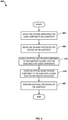
- Figure 4 illustrates an example process 400 for fabricating MUX and DEMUX devices.
- the process 400 may be performed to fabricate one or more optical MUX and/or DEMUX devices, such as, for example, the MUX device 100 of Figure 1 , and the DEMUX devices 200 and 300 of Figures 2 and 3 .
- the process 400 will now be described in reference to Figures 1 , 2 and 3 .
- the process 400 begins with the mounting of one or more semiconductor laser components on a substrate (block 404).
- the semiconductor laser components 120 e.g., VCSELs
- the substrate 110 e.g., VCSELs
- VCSELs may be mounted, in flip-chip fashion, for example, to the substrate 110.
- one or more photodetector devices may be mounted to the substrate 110 (408).
- an optical multiplexer component is coupled to the substrate aligned with the one or more semiconductor laser components.
- the optical MUX component 130 is coupled to the substrate in alignment with the four semiconductor laser components 120 such that respective pairs of laser beams of first, second, third and fourth wavelengths, are received from respective ones of the four semiconductor laser components 120.
- the MUX component may be coupled as a completed component.
- the various wavelength selective filters 135, the reflectors 140 and walls of the optical MUX component 130 may be formed using, but not limited to, semiconductor, MEMS and thin-film fabrication techniques.
- an optical de-multiplexer component may be coupled to the substrate aligned with the one or more photodetector devices.
- the optical DEMUX component 230 may be coupled to the substrate in alignment with the four photodetector devices 220 such that respective pairs of laser beams of first, second, third and fourth wavelengths, are directed to respective ones of the four photodetector devices 220.
- the optical DEMUX component 230 may be coupled to the substrate in alignment with a single photodetector device 320.
- the optical DEMUX component may be coupled as a completed component.
- the various wavelength selective filters 235, the reflectors 240 and walls of the DEMUX device 230 are formed using, but not limited to, semiconductor, MEMS and thin-film fabrication techniques.
- the semiconductor laser components may be coupled to laser driver integrated circuits, and the photodetector devices may be coupled to transimpedance amplifier integrated circuits.
- fiber optic cables, ferules, optical connectors, and/or interfaces configured to be coupled to fiber optic cables may be coupled to the substrate in alignment with the MUX and DEMUX devices.
- the functions performed at blocks 404-420 may be repeated until all semiconductor devices, optical devices and optical fiber assemblies have been attached to the substrate and/or to other devices such as integrated circuits.
- the process 400 illustrated in Figure 4 is an example only and not limiting. In various examples, the process 400 may be altered, for example, by having steps or blocks added, removed, rearranged, combined, and/or performed concurrently.
Landscapes
- Physics & Mathematics (AREA)
- General Physics & Mathematics (AREA)
- Optics & Photonics (AREA)
- Engineering & Computer Science (AREA)
- Computer Networks & Wireless Communication (AREA)
- Signal Processing (AREA)
- Electromagnetism (AREA)
- Optical Couplings Of Light Guides (AREA)
- Semiconductor Lasers (AREA)
Description
- Wave division multiplexing (WDM) is a method of communication that may be used to communicate multiple channels over a single fiber optic cable where each signal is transmitted with a distinct wavelength beam. WDM systems may utilize multiple fibers in order to increase the capacity.
-
US 2004/0218875 describes a VCSEL Array configuration for a parallel WDM transmitter. -
US 6,419,404 relates to a compact multiwavelength transmitter module for multimode fiber optic ribbon cable. -
US 2012/0189306 describes multilaser transmitter optical subassemblies for optoelectronic modules. - ALI M E ET AL: "MAUI: Enabling Fiber-to-the-Processor With Parallel Multiwavelength Optical Interconnects ",JOURNAL OF LIGHTWAVE TECHNOLOGY, IEEE SERVICE CENTER, NEW YORK, NY, US, vol. 22, no. 9, 1 September 2004 (2004-09-01), pages 2043-2054, XP011118631,ISSN: 0733-8724 discloses combining single VCSEL beams in a zig-zag block with mirrors and filters
- For a more complete understanding of various examples, reference is now made to the following description taken in connection with the accompanying drawings in which:
-
Figure 1 illustrates an example multiplexer (MUX) device; -
Figure 2 illustrates a first example de-multiplexer (DEMUX) device; -
Figure 3 illustrates a second example DEMUX device; and -
Figure 4 illustrates an example process for fabricating MUX and DEMUX devices. - Wavelength division multiplexing (WDM) is an approach to scale bandwidth density in datacenters without the need to increase fiber count over multiple generations. Example systems and methods described herein may provide a two dimensional (2D) WDM optoelectronic (OE) engine. The OE engine may be composed of the following components: 1) 2D vertical cavity surface emitting laser (VCSEL) and/or surface illuminated photodetector (SI-PD) arrays, 2) zig-zag optical multiplexer and/or de-multiplexer (MUX/DEMUX) components, 3) 2D output/input coupling interfaces, and 4) 2D fiber (e.g., ferules/cables) arrays. The example systems may take advantage of the 2D wafer scale fabrication of VCSELs and SI-PDs to construct 2D WDM Tx (transmit) and Rx (receive) OE engines.
- The example systems and methods described herein may provide a path to efficiently use embedded fiber infrastructure in datacenters by increasing the bandwidth density and gracefully scaling bandwidth demands from generation to generation without having to increase fiber count.
-
Figure 1 illustrates an example multiplexer (MUX)device 100 formed on a substrate (e.g., a printed circuit board or PCB) 110 and including a plurality of semiconductor laser components (e.g., VCSELs) 120, and an optical MUX component (e.g., a zig-zag MUX component) 130 coupled to two optical fibers 150-1 and 150-2. In this example, theMUX device 100 includes four semiconductor laser components 120-1, 120-2, 120-3 and 120-4, but other numbers of semiconductor laser components 120 of at least two may be used, depending, for example, on the size of theMUX device 100. Thesubstrate 110 is a PCB in this example, but other substrates may be used. - The semiconductor laser components 120 may be mounted in a flip-chip fashion on the
substrate 110 as illustrated inFigure 1 . In thisexample MUX device 100, each of the semiconductor laser components 120 includes two lasers (e.g., VCSELs) 125. The semiconductor laser components 120 emit different wavelength laser beams to provide for the WDM capabilities. For example, the semiconductor laser component 120-1 includes a first laser 125-1 and a second laser 125-2 that each emit a laser beam of a first wavelength, the semiconductor laser component 120-2 includes a third laser 125-3 and a fourth laser 125-4 that each emit a laser beam of a second wavelength, the semiconductor laser component 120-3 includes a fifth laser 125-5 and a sixth laser 125-6 that each emit a laser beam of a third wavelength, and the semiconductor laser component120-4 includes a seventh laser 125-7 and an eighth laser 125-8 that each emit a laser beam of a fourth wavelength. The first, second, third and fourth wavelengths are each a different wavelength. - The
optical MUX component 130 receives the multiple laser beams from the semiconductor laser components 120 and couples these laser beams to the two fibers 150-1 and 150-2 via two output interfaces 145-1 and 145-2. The output interfaces 145 may be an antireflection coated surface, collimator lenses, high contrast grating lens, prisms, or other form of coupling micro-optics. - The
optical MUX component 130 includes three reflectors (e.g., relay mirrors) 140-1, 140-2 and 140-3 and three wavelength selective filters 135-1, 135-2 and 135-3. As an alternative to three separate reflectors 140-1, 140-2 and 140-3, a single reflector 140 could be used in some examples. Each of the wavelength selective filters 135 allow a certain wavelength, or range of wavelengths, of light to pass through substantially unaffected while reflecting other wavelengths. For example, the first wavelength selective filter 135-1 allows the laser beams of the second wavelength emitted from the lasers 125-3 and 125-4 to pass while reflecting the laser beams of the first wavelength that are emitted from the lasers 125-1 and 125-2. Similarly, the second wavelength selective filter 135-2 allows the laser beams of the third wavelength emitted from the lasers 125-5 and 125-6 to pass while reflecting the laser beams of the first and second wavelengths and the third wavelength selective filter 135-3 allows laser beams of the fourth wavelength emitted from the lasers 125-7 and 125-8 to pass while reflecting the laser beams of the first, second and third wavelengths. In this way, theoptical MUX component 130 is able to couple all eight laser beams onto the output interfaces 145-1 and 145-2, which then couples the laser beams to the first and second fibers 150-1 and 150-2. - The reflectors 140, the wavelength selective filters 135 and the lasers 125 are positioned relative to each other such that a first one of the laser beams of each wavelength, the first, second, third and fourth wavelengths in this example, are directed to the first output interface 145-1, while a second one of the laser beams of each wavelength are directed to the second output interface 145-2. The output interfaces 145-1 and 145-2 couple the combined or collimated sets of first and second ones of the laser beams to the first and second fibers 150-1 and 150-2, respectively.
- The
example MUX device 100 uses VCSELs that emit lasers vertically away from thesubstrate 110 and theoptical MUX component 130 is positioned above the semiconductor laser components 120. In other example MUX devices, other orientations of optical MUX component and semiconductor laser components may be used. In other examples, the MUXdevice 100 uses VCSELs with integrated lenses to collimate and/or tilt the laser emission from the VCSEL. - The
example MUX device 100 illustrates a single row of semiconductor laser components 120, single row of mirrors 140, and a single row of output fibers 150. However, multiple rows of semiconductor laser components 120, multiple rows of filters 135, multiple rows of mirrors 140, and multiple rows of output fibers 150 may be provided in two dimensional arrays (e.g., by replicating multiple rows into or out of the page as shown inFigure 1 ) in order to increase capacity and provide a compact device to take advantage of two dimensional semiconductor laser arrays and/or two dimensional fiber arrays. In some examples, the multiple fibers may be contained in a ferule or optical connector. In addition, a MUX device may include a first array of semiconductor laser components 120 with afirst MUX component 130 on a left portion of thesubstrate 110, as shown inFigure 1 , as well as a second array of semiconductor laser components 120 and asecond MUX component 130 positioned in mirror-fashion on the right side of thesubstrate 110. In other examples, the first and second MUX components are a single unit, rather than distinct parts. - The example semiconductor laser components 120 are illustrated with two lasers 125. However, semiconductor laser components with three or more lasers per component may also be used. A factor that may limit the number of lasers per semiconductor laser component is the resulting angle of incidence of the lasers on the reflectors 140 and the wavelength selective filters 135. Angle of incidences less than or equal to 15 degrees may be used in most applications, for example in polarization independent applications. If polarization locked VCSELs are employed, the angle of incidence can be larger than 15 degrees. A thicker
optical MUX component 130 may allow for greater numbers of lasers per component at the expense of athicker MUX device 100. The MUXdevice 100 may be preferably two millimeters thick or less. -
Figure 2 illustrates a first example de-multiplexer (DEMUX)device 200 formed onsubstrate 110 and including a plurality of photodetector devices (e.g., SI-PDs) 220, and an optical DEMUX component (e.g., a zig-zag DEMUX component) 230 coupled to two input fibers 150-3 and 150-4. In this example, theDEMUX device 200 includes four photodetector devices 220-1, 220-2, 220-3 and 220-4, but other numbers of photodetector devices 220 may be used, depending, for example, on the number of unique wavelengths to demultiplex. In some examples, the photodetector devices 220 may be integrated with lenses to focus and/or tilt the incident light for efficient coupling to the photodetector. - In various examples, each photodetector device 220 includes multiple photodetectors. In the example illustrated in
Figure 2 , each photodetector device 220 may have two photodetectors. The photodetector devices 220 may be mounted in flip-chip fashion on thesubstrate 110 as illustrated inFigure 2 . In thisexample DEMUX device 200, each of the photodetector devices 220 may be configured to detect different wavelength laser beams to provide for WDM receiver capabilities. For example, the photodetector device 220-1 may detect laser beams of a first wavelength, the photodetector device 220-2 may detect laser beams of a second wavelength, the photodetector device 220-3 may detect laser beams of a third wavelength, and the photodetector device 220-4 may detect laser beams of a fourth wavelength. The first, second, third and fourth wavelengths are each a different wavelength. The first, second, third and fourth wavelengths detected by the photodetector devices 220 may be the same or different respective wavelengths of the first, second, third and fourth wavelengths emitted by the semiconductor laser components 120 discussed above in reference toFigure 1 . - The
optical DEMUX component 230 receives first and second sets of multiple different wavelength laser beams from a third fiber 150-3 and a fourth fiber 150-4 via a first input interface (e.g., a collimator, coupling lens or prism or high-contrast grating lens) 245-1 and a second input interface 245-2, respectively. TheDEMUX component 230 couples these laser beams to the four photodetector devices 220 using three reflectors 240-1, 240-2 and 240-3 (e.g., relay mirrors) in combination with three wavelength selective filters 235-1, 235-2 and 235-3 in a fashion similar to theMUX component 130 inFigure 1 . - As an alternative to three separate reflectors 240-1, 240-2 and 240-3, a single reflector 240 could be used in some examples. Each of the wavelength selective filters 235 may be configured to allow a certain wavelength, or range of wavelengths, of light to pass through substantially unaffected while reflecting other wavelengths. For example, the first wavelength selective filter 235-1 may allow the laser beams of the second wavelength detected by the second photodetector device 220-2 to pass while reflecting the laser beams of the first wavelength that are detected by the first photodetector device 220-1. Similarly, the second wavelength selective filter 235-2 may allow the laser beams of the third wavelength detected by the third photodetector device 220-3 to pass while reflecting the laser beams of the first and second wavelengths and the third wavelength selective filter 235-3 may allow laser beams of the fourth wavelength detected by the fourth photodetector device to pass while reflecting the laser beams of the first, second and third wavelengths. In this way, the
optical DEMUX component 230 is able to focus all eight laser beams received from the input interfaces 245-1 and 245-2 onto the proper photodetecor devices 220. - The reflectors 240, the wavelength selective filters 235 and the photodetector devices 220 are positioned relative to each other such that first and second ones of the laser beams of each wavelength, the first, second, third and fourth wavelengths in this example, are directed to the each respective photodetector device 220.
- The
example DEMUX device 200 uses SI-PDs that detect light on an upper surface facing thesubstrate 110 and theoptical DEMUX component 230 is positioned above the photodetector components 220. In other example DEMUX devices, other orientations of optical DEMUX component and photodetector devices may be used. - The
example DEMUX device 200 illustrates a single row of photodetector devices 220 and a single row of input fibers 150. However, multiple rows of photodetector devices 220, multiple rows of filters 235, multiple rows of mirrors 240, and multiple rows of input fibers 150 may be provided in two dimensional arrays (e.g., by replicating multiple rows into or out of the page as shown inFigure 2 ) in order to increase capacity and provide a compact device to take advantage of two dimensional photodetector arrays and/or two dimensional fiber arrays. In addition, a DEMUX device may include a first array of photodetector devices 220 with afirst DEMUX component 230 on a left portion of thesubstrate 110, as shown inFigure 2 , as well as a second array of photodetector devices 220 and asecond DEMUX component 230 positioned in mirror-fashion on the right side of thesubstrate 110. In other examples, the first and second DEMUX components are a single unit, rather than distinct parts. -
Figure 3 illustrates a secondexample DEMUX device 300 formed onsubstrate 110 and including a single photodetector device (e.g., SI-PD) 320 in place of the multiple photodetector devices 220 shown inFigure 2 . Thesingle photodetector device 320 may be configured to detect all four wavelengths of light that are received from the input fibers 150-3 and 150-4 via the input interfaces 245-1 and 245-2. In this regard, various examples of thesingle photodetector device 320 may include multiple photodetectors. The configuration ofDEMUX device 300 may be suitable when the range of wavelengths between the first, second, third and fourth wavelengths is small enough to be detected by thesingle photodetector device 320. In contrast, theDEMUX device 200, which utilizes four photodetector devices 220, may be used for cases where the first, second, third and fourth wavelengths comprise larger ranges of wavelengths. In another example, theMUX device 100 ofFigure 1 , theDEMUX device 200 ofFigure 2 or theDEMUX device 300 ofFigure 3 may be positioned on thesubstrate 110 in a mirror fashion to build a transceiver where theMUX device 100 andDEMUX device 200 may be a single unit. -
Figure 4 illustrates anexample process 400 for fabricating MUX and DEMUX devices. In various examples, theprocess 400 may be performed to fabricate one or more optical MUX and/or DEMUX devices, such as, for example, theMUX device 100 ofFigure 1 , and theDEMUX devices Figures 2 and3 . Theprocess 400 will now be described in reference toFigures 1 ,2 and3 . - In the example illustrated in
Figure 4 , theprocess 400 begins with the mounting of one or more semiconductor laser components on a substrate (block 404). For example, the semiconductor laser components 120 (e.g.,VCSELs) are mounted to thesubstrate 110. VCSELs may be mounted, in flip-chip fashion, for example, to thesubstrate 110. - Upon the semiconductor laser components being mounted on the
substrate 110, one or more photodetector devices (e.g., the photodetector devices 220 and/or 320) may be mounted to the substrate 110 (408). - At
block 412, after the one or more semiconductor laser components are mounted to the substrate at 404, an optical multiplexer component is coupled to the substrate aligned with the one or more semiconductor laser components. For example, theoptical MUX component 130 is coupled to the substrate in alignment with the four semiconductor laser components 120 such that respective pairs of laser beams of first, second, third and fourth wavelengths, are received from respective ones of the four semiconductor laser components 120. The MUX component may be coupled as a completed component. The various wavelength selective filters 135, the reflectors 140 and walls of theoptical MUX component 130 may be formed using, but not limited to, semiconductor, MEMS and thin-film fabrication techniques. - At
block 416, after the one or more photodetector devices are mounted to the substrate at 408, an optical de-multiplexer component may be coupled to the substrate aligned with the one or more photodetector devices. For example, theoptical DEMUX component 230 may be coupled to the substrate in alignment with the four photodetector devices 220 such that respective pairs of laser beams of first, second, third and fourth wavelengths, are directed to respective ones of the four photodetector devices 220. Alternatively, theoptical DEMUX component 230 may be coupled to the substrate in alignment with asingle photodetector device 320. The optical DEMUX component may be coupled as a completed component. The various wavelength selective filters 235, the reflectors 240 and walls of theDEMUX device 230 are formed using, but not limited to, semiconductor, MEMS and thin-film fabrication techniques. - At
block 420, other additional processing may be performed on the substrate. For example, the semiconductor laser components may be coupled to laser driver integrated circuits, and the photodetector devices may be coupled to transimpedance amplifier integrated circuits. Also, fiber optic cables, ferules, optical connectors, and/or interfaces configured to be coupled to fiber optic cables may be coupled to the substrate in alignment with the MUX and DEMUX devices. - The functions performed at blocks 404-420 may be repeated until all semiconductor devices, optical devices and optical fiber assemblies have been attached to the substrate and/or to other devices such as integrated circuits. The
process 400 illustrated inFigure 4 is an example only and not limiting. In various examples, theprocess 400 may be altered, for example, by having steps or blocks added, removed, rearranged, combined, and/or performed concurrently. - The foregoing description of various examples has been presented for purposes of illustration and description. The foregoing description is not intended to be exhaustive or limiting to the examples disclosed, and modifications and variations are possible in light of the above teachings or may be acquired from practice of various examples. The examples discussed herein were chosen and described in order to explain the principles and the nature of various examples of the present disclosure and its practical application to enable one skilled in the art to utilize the present disclosure in various examples and with various modifications as are suited to the particular use contemplated. The features of the examples described herein may be combined in all possible combinations of methods, apparatus, modules, systems, and computer program products.
- It is also noted herein that while the above describes examples, these descriptions should not be viewed in a limiting sense. Rather, there are several variations and modifications which may be made without departing from the scope as defined in the appended claims.
Claims (11)
- A device comprising:a first semiconductor component (120-1) comprising at least two lasers (125-1, 125-2) to emit light at a first wavelength;a second semiconductor component (120-2) comprising at least two lasers (125-3, 125-4) to emit light at a second wavelength, the first wavelength being different from the second wavelength; andan optical multiplexer component (130) to receive light from two lasers (125-1, 125-2) at the first wavelength and light from two lasers (125-3, 125-4) at the second wavelength, characterised in that the optical multiplexer component (130) includes:a first output interface (145-1) to couple light from one laser at the first wavelength and light from one laser at the second wavelength to a first optical fiber (150-1), anda second output interface (145-2) to couple light from one laser at the first wavelength and light from one laser at the second wavelength beams to a second optical fiber (150-2); and in that:
the optical multiplexer component (130) further comprises:one reflector to reflect (140-2) substantially all wavelengths of light; andone wavelength selective filter (135-2) to allow light at either the first wavelength or the second wavelength to pass through and to reflect other wavelengths of light,wherein, the one reflector (140-2) and the one wavelength selective filter (135-2) are positioned relative to the first and second semiconductor components (120) to direct light from one laser at the first wavelength and light from one laser at the second wavelength to the first output interface (145-1) and to direct light from one laser at the first wavelength and light from one laser at the second wavelength to the second output interface (145-2). - The device of claim 1further comprising an optical de-multiplexer component (230) having:a first input interface to receive a first input signal from a third optical fiber (150-3), the first input signal including light at the first wavelength and light at the second wavelength;a second input interface to receive a second input signal from a fourth optical fiber (150-4), the second input signal including light at the first wavelength and light at the second wavelength; andwherein the optical de-multiplexer component (230) directs light at the first wavelength from the first interface and light at the first wavelength from the second interface to a first photodetector (220-1) and directs light at the second wavelength from the first interface and
light at the second wavelength from the second interface to a second photodetector (220-2). - The device of claim 1, wherein the optical multiplexer component (130) is coupled to a substrate (110), wherein the laser (125) emit light vertically away from the substrate and the optical multiplexer component (130) is positioned above the first and second semiconductor components (120).
- The device of claim 3, wherein at least a portion of the first and second semiconductor components (120) is mounted in flip-chip fashion on the substrate (110).
- The device of claim 2, wherein the optical de-multiplexer component (230) comprises:at least one reflector (240) to reflect substantially all wavelengths of light; andat least one wavelength selective filter (235) to allow light at either the first wavelength or the second wavelength to pass through and to reflect other wavelengths of light,wherein, the at least one reflector (240) and the at least one wavelength selective filter (235) are positioned relative to the first and second photodetector devices to direct light from the first input interface at the first wavelength and light from the second input interface at the first wavelength to the first photodetector (220-1) and to direct light from the first input interface at the second wavelength and light from the second input interface at the second wavelength the second photodetector (220-2).
- A method (400) comprising:mounting (404) a plurality of semiconductor components (120) on a substrate (110), the plurality of semiconductor components including at least a first semiconductor component (120-1) comprising at least two first lasers (125-1, 125-2) configured to emit first wavelength laser beams and a second semiconductor component (120-2) comprising at least two second lasers (120-3, 120-4) configured to emit second wavelength laser beams, the first wavelength being different than the second wavelength;coupling (412), to the substrate (110) in alignment with the at least first and second semiconductor components (120), an optical multiplexer (130) component configured to receive the two first wavelength beams and the two second wavelength beams, the optical multiplexer component (130) comprising:a first output interface (145-1) configured to couple a first one of the first wavelength beams and a first one of the second wavelength beams to a first optical fiber (150-1), and a second output interface (145-2) configured to couple a second one of the first wavelength beams and a second one of the second wavelength beams to a second optical fiber (150-2), and whereincoupling (412) the optical multiplexer component comprises forming one wavelength selective filter (135) and one reflector layer (140) above the plurality of semiconductor components (120),the one wavelength selective filter (135) and one reflector (140) being configured to receive the first and second wavelength beams and direct the first ones of the first and second wavelength beams on the first output interface and direct the second ones of the first and second wavelength beams on the second output interface.
- The method of claim 6, wherein mounting the plurality of semiconductor devices further includes mounting (408) at least a first photodetector device to the substrate, the method further comprising:coupling (416), to the substrate in alignment with the at least one photodetector device, an optical de-multiplexer component (230), the optical de-multiplexer component comprising:a first input interface configured to receive a first input signal from a third optical fiber (150-3), the first input signal including a first beam of a third wavelength and a first beam of a fourth wavelength, anda second input interface configured to receive a second input signal from a fourth optical fiber (150-4), the second input signal including a second beam of the third wavelength and a second beam of the fourth wavelength;wherein the optical de-multiplexer component (280) is configured to direct the first and second beams of the third wavelength and the first and second beams of the fourth wavelength on the first photodetector device (220-1)
- A printed circuit board assembly (100), comprising the device of claim 2 and at least the first photodetector (220-1) and the second photodetector (220-2) coupled to a substrate (110).
- The printed circuit board assembly of claim 8, wherein the optical multiplexer component (130) is positioned above the first and second semiconductor components (120).
- The printed circuit board assembly of claim 8, wherein the first and second semiconductor devices (120) are mounted in flip-chip fashion on the substrate (110).
- The printed circuit board assembly of claim 8, wherein the optical de-multiplexer component (230) further comprises:at least one reflector (240) to reflect substantially all wavelengths of light; andat least one wavelength selective filter (235) to allow either the first wavelength beams or the second wavelength beams to pass through and to reflect other wavelengths of light,wherein, the at least one reflector (240) and the at least one wavelength selective filter (235) are positioned relative to the first and second photodetector devices to direct the first beams of the first and second wavelength on the first photodetector device and to direct the second beams of the first and second wavelength on the second photodetector device.
Applications Claiming Priority (1)
| Application Number | Priority Date | Filing Date | Title |
|---|---|---|---|
| PCT/US2013/067880 WO2015065459A1 (en) | 2013-10-31 | 2013-10-31 | Multiplexed optoelectronic engines |
Publications (3)
| Publication Number | Publication Date |
|---|---|
| EP3063574A1 EP3063574A1 (en) | 2016-09-07 |
| EP3063574A4 EP3063574A4 (en) | 2017-10-11 |
| EP3063574B1 true EP3063574B1 (en) | 2022-03-02 |
Family
ID=53004862
Family Applications (1)
| Application Number | Title | Priority Date | Filing Date |
|---|---|---|---|
| EP13896285.7A Active EP3063574B1 (en) | 2013-10-31 | 2013-10-31 | Multiplexed optoelectronic engines |
Country Status (4)
| Country | Link |
|---|---|
| US (1) | US10007065B2 (en) |
| EP (1) | EP3063574B1 (en) |
| CN (1) | CN105659127B (en) |
| WO (1) | WO2015065459A1 (en) |
Families Citing this family (24)
| Publication number | Priority date | Publication date | Assignee | Title |
|---|---|---|---|---|
| US20160327746A1 (en) * | 2014-01-25 | 2016-11-10 | Hewlett-Packard Development Company, L.P. | Bidirectional optical multiplexing employing a high contrast grating |
| CN106154444B (en) * | 2015-04-28 | 2018-12-28 | 华为技术有限公司 | Optical transceiver and optic communication product |
| CN104865654A (en) * | 2015-05-18 | 2015-08-26 | 无锡清辉光电科技有限公司 | Substrate, laser array, light detector array, module, and transmitting and receiving module |
| US10859437B2 (en) * | 2016-05-10 | 2020-12-08 | Chromation, Inc. | Integration of optical components within a folded optical path |
| WO2018053442A1 (en) * | 2016-09-16 | 2018-03-22 | Kaiam Corp. | Qsfp double density module |
| US10313045B2 (en) | 2016-11-17 | 2019-06-04 | Alliance Fiber Optic Products, Inc. | Wavelength-division multiplexing optical assembly with increased lane density |
| US10551569B2 (en) | 2017-02-02 | 2020-02-04 | Alliance Fiber Optic Products, Inc. | Wavelength-division multiplexing optical assembly with multiple collimator sets |
| US9995880B1 (en) | 2017-03-31 | 2018-06-12 | Foxconn Interconnect Technology Limited | Wavelength division multiplexing and demultiplexing in optical communications modules, and methods |
| JP6969154B2 (en) * | 2017-05-16 | 2021-11-24 | 富士通オプティカルコンポーネンツ株式会社 | Optical transmitter and receiver |
| EP3422614B1 (en) * | 2017-06-27 | 2023-09-13 | Huawei Technologies Co., Ltd. | Optical wavelength division multiplexing device |
| EP3665519A4 (en) * | 2017-08-10 | 2021-04-28 | Luxtera, Inc. | CWDM FREE SPACE MULTIPLEXER / DEMULTIPLEXER FOR INTEGRATING A PHOTONIC PLATFORM ON SILICON |
| US10355805B2 (en) * | 2017-08-10 | 2019-07-16 | Luxtera, Inc. | Method and system for a free space CWDM MUX/DEMUX for integration with a grating coupler based silicon photonics platform |
| US11022756B2 (en) * | 2017-10-12 | 2021-06-01 | Luxtera Llc | Method and system for near normal incidence MUX/DEMUX designs |
| JP7241461B2 (en) * | 2017-12-19 | 2023-03-17 | 日本ルメンタム株式会社 | Optical multiplexer/demultiplexer, optical subassembly and optical module |
| FR3076356B1 (en) * | 2017-12-29 | 2020-01-31 | Cailabs | Monolithic cavity for the manipulation of light |
| JP2020021013A (en) * | 2018-08-03 | 2020-02-06 | 富士通株式会社 | WDM optical module, WDM optical module, and optical module |
| US10924185B2 (en) * | 2018-08-06 | 2021-02-16 | Hewlett Packard Enterprise Development Lp | Systems and methods of dual-side array bi-directional CWDM micro-optics |
| US11624836B2 (en) * | 2019-09-24 | 2023-04-11 | Continental Autonomous Mobility US, LLC | Detection of damage to optical element of illumination system |
| US11005588B1 (en) | 2019-10-31 | 2021-05-11 | Alliance Fiber Optic Products, Inc. | Wavelength division multiplexing with signal entry and exit in same routing surface to increase channel density |
| CN115104053B (en) * | 2020-02-21 | 2023-10-20 | 三菱电机株式会社 | Integrated optical module |
| US11750316B2 (en) | 2020-07-28 | 2023-09-05 | Alliance Fiber Optic Products, Inc. | Wavelength division multiplexing with parallel arrayed signal paths for increased channel density |
| US11973580B2 (en) | 2021-09-30 | 2024-04-30 | Corning Research & Development Corporation | Redundant wavelength division multiplexing devices and methods for processing light using same |
| WO2023102769A1 (en) * | 2021-12-08 | 2023-06-15 | Lumentum Operations Llc | Multiple filter package configuration for wavelength division multiplexer |
| US12438620B2 (en) * | 2022-10-31 | 2025-10-07 | Avago Technologies International Sales Pte. Limited | Laser with optical signal management capability |
Family Cites Families (14)
| Publication number | Priority date | Publication date | Assignee | Title |
|---|---|---|---|---|
| US6198864B1 (en) * | 1998-11-24 | 2001-03-06 | Agilent Technologies, Inc. | Optical wavelength demultiplexer |
| US6419404B1 (en) | 1999-07-01 | 2002-07-16 | The Regents Of The University Of California | Compact multiwavelength transmitter module for multimode fiber optic ribbon cable |
| US6563976B1 (en) * | 2000-05-09 | 2003-05-13 | Blaze Network Products, Inc. | Cost-effective wavelength division multiplexer and demultiplexer |
| US6751379B2 (en) * | 2000-11-01 | 2004-06-15 | Intel Corporation | System and method for collimating and redirecting beams in a fiber optic system |
| US6804429B2 (en) * | 2001-02-09 | 2004-10-12 | The Board Of Trustees Of The Leland Stanford Junior University | Reconfigurable wavelength multiplexers and filters employing micromirror array in a gires-tournois interferometer |
| US6870976B2 (en) | 2001-03-13 | 2005-03-22 | Opnext, Inc. | Filter based multiplexer/demultiplexer component |
| US7004645B2 (en) * | 2003-04-30 | 2006-02-28 | Agilent Technologies, Inc. | VCSEL array configuration for a parallel WDM transmitter |
| US7019907B2 (en) | 2003-11-25 | 2006-03-28 | Intel Corporation | Integrated lithium niobate based optical transmitter |
| US6937786B2 (en) * | 2004-01-09 | 2005-08-30 | Agilent Technologies, Inc. | Parallel multiwavelength optical subassembly |
| US8346087B2 (en) * | 2007-09-28 | 2013-01-01 | Oracle America, Inc. | Wavelength-division multiplexing for use in multi-chip systems |
| US8457165B2 (en) * | 2010-05-26 | 2013-06-04 | Google Inc. | Tunable multi-wavelength semiconductor laser array for optical communications based on wavelength division multiplexing |
| US8625989B2 (en) | 2011-01-21 | 2014-01-07 | Finisar Corporation | Multi-laser transmitter optical subassemblies for optoelectronic modules |
| KR20130037568A (en) | 2011-10-06 | 2013-04-16 | 한국전자통신연구원 | Optical line terminal in passive optical network based on tdma and method for process optical signal thereof |
| CN105556358A (en) * | 2013-08-21 | 2016-05-04 | 慧与发展有限责任合伙企业 | Device including mirrors and filters to operate as a multiplexer or de-multiplexer |
-
2013
- 2013-10-31 CN CN201380080392.0A patent/CN105659127B/en active Active
- 2013-10-31 WO PCT/US2013/067880 patent/WO2015065459A1/en not_active Ceased
- 2013-10-31 EP EP13896285.7A patent/EP3063574B1/en active Active
- 2013-10-31 US US15/030,427 patent/US10007065B2/en active Active
Also Published As
| Publication number | Publication date |
|---|---|
| CN105659127B (en) | 2021-08-20 |
| EP3063574A4 (en) | 2017-10-11 |
| WO2015065459A1 (en) | 2015-05-07 |
| EP3063574A1 (en) | 2016-09-07 |
| US20160246008A1 (en) | 2016-08-25 |
| CN105659127A (en) | 2016-06-08 |
| US10007065B2 (en) | 2018-06-26 |
Similar Documents
| Publication | Publication Date | Title |
|---|---|---|
| EP3063574B1 (en) | Multiplexed optoelectronic engines | |
| US9429725B2 (en) | Bidirectional parallel optical transceiver module and a method for bidirectionally communicating optical signals over an optical link | |
| US10018787B1 (en) | Multi-channel optical wavelength division multiplexing/demultiplexing (WDM) assembly and methods | |
| JP7346457B2 (en) | Multichannel optical coupler | |
| EP3088928B1 (en) | Optical transceiver and optical communications product | |
| US8625989B2 (en) | Multi-laser transmitter optical subassemblies for optoelectronic modules | |
| US9322987B2 (en) | Multicore fiber coupler between multicore fibers and optical waveguides | |
| US9323013B2 (en) | Bidirectional optical communications module having an optics system that reduces optical losses and increases tolerance to optical misalignment | |
| TWI536757B (en) | Bidirectional optical data communications module | |
| US10924185B2 (en) | Systems and methods of dual-side array bi-directional CWDM micro-optics | |
| CN103201969A (en) | Optical multiplexing using laser arrays | |
| US9995880B1 (en) | Wavelength division multiplexing and demultiplexing in optical communications modules, and methods | |
| CN107966773A (en) | Light emitting secondary module and optical module | |
| US10502908B2 (en) | Long-reach active optical cable | |
| US10795170B2 (en) | Multi-channel optical multiplexer or demultiplexer | |
| US12204150B2 (en) | System and method for optical communications using CWDM ferrule mated to a non-CWDM ferrule | |
| US11747566B2 (en) | Coupling multiple optical channels using a z-block | |
| US20120213527A1 (en) | Optoelectronic device for bidirectionally transporting information through optical fibers and method of manufacturing such a device | |
| US12212364B2 (en) | Miniaturized multichannel wavelength division multiplexing optical module | |
| CN111123432A (en) | Polarization diversity optical interface assembly, optical connector and coupling method |
Legal Events
| Date | Code | Title | Description |
|---|---|---|---|
| PUAI | Public reference made under article 153(3) epc to a published international application that has entered the european phase |
Free format text: ORIGINAL CODE: 0009012 |
|
| 17P | Request for examination filed |
Effective date: 20160404 |
|
| AK | Designated contracting states |
Kind code of ref document: A1 Designated state(s): AL AT BE BG CH CY CZ DE DK EE ES FI FR GB GR HR HU IE IS IT LI LT LU LV MC MK MT NL NO PL PT RO RS SE SI SK SM TR |
|
| AX | Request for extension of the european patent |
Extension state: BA ME |
|
| DAX | Request for extension of the european patent (deleted) | ||
| RIC1 | Information provided on ipc code assigned before grant |
Ipc: G02B 6/42 20060101AFI20170530BHEP |
|
| A4 | Supplementary search report drawn up and despatched |
Effective date: 20170908 |
|
| RIC1 | Information provided on ipc code assigned before grant |
Ipc: G02B 6/42 20060101AFI20170904BHEP |
|
| STAA | Information on the status of an ep patent application or granted ep patent |
Free format text: STATUS: EXAMINATION IS IN PROGRESS |
|
| 17Q | First examination report despatched |
Effective date: 20200917 |
|
| REG | Reference to a national code |
Ref country code: DE Ref legal event code: R079 Ref document number: 602013081045 Country of ref document: DE Free format text: PREVIOUS MAIN CLASS: G02B0006125000 Ipc: G02B0006420000 |
|
| RIC1 | Information provided on ipc code assigned before grant |
Ipc: G02B 6/293 20060101ALI20211019BHEP Ipc: G02B 6/42 20060101AFI20211019BHEP |
|
| GRAP | Despatch of communication of intention to grant a patent |
Free format text: ORIGINAL CODE: EPIDOSNIGR1 |
|
| STAA | Information on the status of an ep patent application or granted ep patent |
Free format text: STATUS: GRANT OF PATENT IS INTENDED |
|
| INTG | Intention to grant announced |
Effective date: 20211207 |
|
| GRAS | Grant fee paid |
Free format text: ORIGINAL CODE: EPIDOSNIGR3 |
|
| GRAA | (expected) grant |
Free format text: ORIGINAL CODE: 0009210 |
|
| STAA | Information on the status of an ep patent application or granted ep patent |
Free format text: STATUS: THE PATENT HAS BEEN GRANTED |
|
| AK | Designated contracting states |
Kind code of ref document: B1 Designated state(s): AL AT BE BG CH CY CZ DE DK EE ES FI FR GB GR HR HU IE IS IT LI LT LU LV MC MK MT NL NO PL PT RO RS SE SI SK SM TR |
|
| REG | Reference to a national code |
Ref country code: GB Ref legal event code: FG4D |
|
| REG | Reference to a national code |
Ref country code: CH Ref legal event code: EP Ref country code: AT Ref legal event code: REF Ref document number: 1472727 Country of ref document: AT Kind code of ref document: T Effective date: 20220315 |
|
| REG | Reference to a national code |
Ref country code: DE Ref legal event code: R096 Ref document number: 602013081045 Country of ref document: DE |
|
| REG | Reference to a national code |
Ref country code: IE Ref legal event code: FG4D |
|
| REG | Reference to a national code |
Ref country code: LT Ref legal event code: MG9D |
|
| REG | Reference to a national code |
Ref country code: NL Ref legal event code: MP Effective date: 20220302 |
|
| PG25 | Lapsed in a contracting state [announced via postgrant information from national office to epo] |
Ref country code: SE Free format text: LAPSE BECAUSE OF FAILURE TO SUBMIT A TRANSLATION OF THE DESCRIPTION OR TO PAY THE FEE WITHIN THE PRESCRIBED TIME-LIMIT Effective date: 20220302 Ref country code: RS Free format text: LAPSE BECAUSE OF FAILURE TO SUBMIT A TRANSLATION OF THE DESCRIPTION OR TO PAY THE FEE WITHIN THE PRESCRIBED TIME-LIMIT Effective date: 20220302 Ref country code: NO Free format text: LAPSE BECAUSE OF FAILURE TO SUBMIT A TRANSLATION OF THE DESCRIPTION OR TO PAY THE FEE WITHIN THE PRESCRIBED TIME-LIMIT Effective date: 20220602 Ref country code: LT Free format text: LAPSE BECAUSE OF FAILURE TO SUBMIT A TRANSLATION OF THE DESCRIPTION OR TO PAY THE FEE WITHIN THE PRESCRIBED TIME-LIMIT Effective date: 20220302 Ref country code: HR Free format text: LAPSE BECAUSE OF FAILURE TO SUBMIT A TRANSLATION OF THE DESCRIPTION OR TO PAY THE FEE WITHIN THE PRESCRIBED TIME-LIMIT Effective date: 20220302 Ref country code: ES Free format text: LAPSE BECAUSE OF FAILURE TO SUBMIT A TRANSLATION OF THE DESCRIPTION OR TO PAY THE FEE WITHIN THE PRESCRIBED TIME-LIMIT Effective date: 20220302 Ref country code: BG Free format text: LAPSE BECAUSE OF FAILURE TO SUBMIT A TRANSLATION OF THE DESCRIPTION OR TO PAY THE FEE WITHIN THE PRESCRIBED TIME-LIMIT Effective date: 20220602 |
|
| REG | Reference to a national code |
Ref country code: AT Ref legal event code: MK05 Ref document number: 1472727 Country of ref document: AT Kind code of ref document: T Effective date: 20220302 |
|
| PG25 | Lapsed in a contracting state [announced via postgrant information from national office to epo] |
Ref country code: PL Free format text: LAPSE BECAUSE OF FAILURE TO SUBMIT A TRANSLATION OF THE DESCRIPTION OR TO PAY THE FEE WITHIN THE PRESCRIBED TIME-LIMIT Effective date: 20220302 Ref country code: LV Free format text: LAPSE BECAUSE OF FAILURE TO SUBMIT A TRANSLATION OF THE DESCRIPTION OR TO PAY THE FEE WITHIN THE PRESCRIBED TIME-LIMIT Effective date: 20220302 Ref country code: GR Free format text: LAPSE BECAUSE OF FAILURE TO SUBMIT A TRANSLATION OF THE DESCRIPTION OR TO PAY THE FEE WITHIN THE PRESCRIBED TIME-LIMIT Effective date: 20220603 Ref country code: FI Free format text: LAPSE BECAUSE OF FAILURE TO SUBMIT A TRANSLATION OF THE DESCRIPTION OR TO PAY THE FEE WITHIN THE PRESCRIBED TIME-LIMIT Effective date: 20220302 |
|
| REG | Reference to a national code |
Ref country code: DE Ref legal event code: R082 Ref document number: 602013081045 Country of ref document: DE Representative=s name: FLEUCHAUS & GALLO PARTNERSCHAFT MBB - PATENT- , DE Ref country code: DE Ref legal event code: R082 Ref document number: 602013081045 Country of ref document: DE Representative=s name: FLEUCHAUS & GALLO PARTNERSCHAFT MBB PATENTANWA, DE |
|
| PG25 | Lapsed in a contracting state [announced via postgrant information from national office to epo] |
Ref country code: NL Free format text: LAPSE BECAUSE OF FAILURE TO SUBMIT A TRANSLATION OF THE DESCRIPTION OR TO PAY THE FEE WITHIN THE PRESCRIBED TIME-LIMIT Effective date: 20220302 |
|
| RAP4 | Party data changed (patent owner data changed or rights of a patent transferred) |
Owner name: HEWLETT PACKARD ENTERPRISE DEVELOPMENT LP |
|
| PG25 | Lapsed in a contracting state [announced via postgrant information from national office to epo] |
Ref country code: SM Free format text: LAPSE BECAUSE OF FAILURE TO SUBMIT A TRANSLATION OF THE DESCRIPTION OR TO PAY THE FEE WITHIN THE PRESCRIBED TIME-LIMIT Effective date: 20220302 Ref country code: SK Free format text: LAPSE BECAUSE OF FAILURE TO SUBMIT A TRANSLATION OF THE DESCRIPTION OR TO PAY THE FEE WITHIN THE PRESCRIBED TIME-LIMIT Effective date: 20220302 Ref country code: RO Free format text: LAPSE BECAUSE OF FAILURE TO SUBMIT A TRANSLATION OF THE DESCRIPTION OR TO PAY THE FEE WITHIN THE PRESCRIBED TIME-LIMIT Effective date: 20220302 Ref country code: PT Free format text: LAPSE BECAUSE OF FAILURE TO SUBMIT A TRANSLATION OF THE DESCRIPTION OR TO PAY THE FEE WITHIN THE PRESCRIBED TIME-LIMIT Effective date: 20220704 Ref country code: EE Free format text: LAPSE BECAUSE OF FAILURE TO SUBMIT A TRANSLATION OF THE DESCRIPTION OR TO PAY THE FEE WITHIN THE PRESCRIBED TIME-LIMIT Effective date: 20220302 Ref country code: CZ Free format text: LAPSE BECAUSE OF FAILURE TO SUBMIT A TRANSLATION OF THE DESCRIPTION OR TO PAY THE FEE WITHIN THE PRESCRIBED TIME-LIMIT Effective date: 20220302 Ref country code: AT Free format text: LAPSE BECAUSE OF FAILURE TO SUBMIT A TRANSLATION OF THE DESCRIPTION OR TO PAY THE FEE WITHIN THE PRESCRIBED TIME-LIMIT Effective date: 20220302 |
|
| PG25 | Lapsed in a contracting state [announced via postgrant information from national office to epo] |
Ref country code: IS Free format text: LAPSE BECAUSE OF FAILURE TO SUBMIT A TRANSLATION OF THE DESCRIPTION OR TO PAY THE FEE WITHIN THE PRESCRIBED TIME-LIMIT Effective date: 20220702 Ref country code: AL Free format text: LAPSE BECAUSE OF FAILURE TO SUBMIT A TRANSLATION OF THE DESCRIPTION OR TO PAY THE FEE WITHIN THE PRESCRIBED TIME-LIMIT Effective date: 20220302 |
|
| REG | Reference to a national code |
Ref country code: DE Ref legal event code: R097 Ref document number: 602013081045 Country of ref document: DE |
|
| PLBE | No opposition filed within time limit |
Free format text: ORIGINAL CODE: 0009261 |
|
| STAA | Information on the status of an ep patent application or granted ep patent |
Free format text: STATUS: NO OPPOSITION FILED WITHIN TIME LIMIT |
|
| PG25 | Lapsed in a contracting state [announced via postgrant information from national office to epo] |
Ref country code: DK Free format text: LAPSE BECAUSE OF FAILURE TO SUBMIT A TRANSLATION OF THE DESCRIPTION OR TO PAY THE FEE WITHIN THE PRESCRIBED TIME-LIMIT Effective date: 20220302 |
|
| PGFP | Annual fee paid to national office [announced via postgrant information from national office to epo] |
Ref country code: GB Payment date: 20221118 Year of fee payment: 10 |
|
| 26N | No opposition filed |
Effective date: 20221205 |
|
| PG25 | Lapsed in a contracting state [announced via postgrant information from national office to epo] |
Ref country code: SI Free format text: LAPSE BECAUSE OF FAILURE TO SUBMIT A TRANSLATION OF THE DESCRIPTION OR TO PAY THE FEE WITHIN THE PRESCRIBED TIME-LIMIT Effective date: 20220302 |
|
| PG25 | Lapsed in a contracting state [announced via postgrant information from national office to epo] |
Ref country code: MC Free format text: LAPSE BECAUSE OF FAILURE TO SUBMIT A TRANSLATION OF THE DESCRIPTION OR TO PAY THE FEE WITHIN THE PRESCRIBED TIME-LIMIT Effective date: 20220302 |
|
| REG | Reference to a national code |
Ref country code: CH Ref legal event code: PL |
|
| REG | Reference to a national code |
Ref country code: BE Ref legal event code: MM Effective date: 20221031 |
|
| PG25 | Lapsed in a contracting state [announced via postgrant information from national office to epo] |
Ref country code: LU Free format text: LAPSE BECAUSE OF NON-PAYMENT OF DUE FEES Effective date: 20221031 |
|
| PG25 | Lapsed in a contracting state [announced via postgrant information from national office to epo] |
Ref country code: LI Free format text: LAPSE BECAUSE OF NON-PAYMENT OF DUE FEES Effective date: 20221031 Ref country code: IT Free format text: LAPSE BECAUSE OF FAILURE TO SUBMIT A TRANSLATION OF THE DESCRIPTION OR TO PAY THE FEE WITHIN THE PRESCRIBED TIME-LIMIT Effective date: 20220302 Ref country code: FR Free format text: LAPSE BECAUSE OF NON-PAYMENT OF DUE FEES Effective date: 20221031 Ref country code: CH Free format text: LAPSE BECAUSE OF NON-PAYMENT OF DUE FEES Effective date: 20221031 |
|
| PG25 | Lapsed in a contracting state [announced via postgrant information from national office to epo] |
Ref country code: BE Free format text: LAPSE BECAUSE OF NON-PAYMENT OF DUE FEES Effective date: 20221031 |
|
| PG25 | Lapsed in a contracting state [announced via postgrant information from national office to epo] |
Ref country code: IE Free format text: LAPSE BECAUSE OF NON-PAYMENT OF DUE FEES Effective date: 20221031 |
|
| PG25 | Lapsed in a contracting state [announced via postgrant information from national office to epo] |
Ref country code: HU Free format text: LAPSE BECAUSE OF FAILURE TO SUBMIT A TRANSLATION OF THE DESCRIPTION OR TO PAY THE FEE WITHIN THE PRESCRIBED TIME-LIMIT; INVALID AB INITIO Effective date: 20131031 |
|
| PG25 | Lapsed in a contracting state [announced via postgrant information from national office to epo] |
Ref country code: CY Free format text: LAPSE BECAUSE OF FAILURE TO SUBMIT A TRANSLATION OF THE DESCRIPTION OR TO PAY THE FEE WITHIN THE PRESCRIBED TIME-LIMIT Effective date: 20220302 |
|
| PG25 | Lapsed in a contracting state [announced via postgrant information from national office to epo] |
Ref country code: MK Free format text: LAPSE BECAUSE OF FAILURE TO SUBMIT A TRANSLATION OF THE DESCRIPTION OR TO PAY THE FEE WITHIN THE PRESCRIBED TIME-LIMIT Effective date: 20220302 |
|
| GBPC | Gb: european patent ceased through non-payment of renewal fee |
Effective date: 20231031 |
|
| PG25 | Lapsed in a contracting state [announced via postgrant information from national office to epo] |
Ref country code: GB Free format text: LAPSE BECAUSE OF NON-PAYMENT OF DUE FEES Effective date: 20231031 |
|
| PG25 | Lapsed in a contracting state [announced via postgrant information from national office to epo] |
Ref country code: GB Free format text: LAPSE BECAUSE OF NON-PAYMENT OF DUE FEES Effective date: 20231031 |
|
| PG25 | Lapsed in a contracting state [announced via postgrant information from national office to epo] |
Ref country code: MT Free format text: LAPSE BECAUSE OF FAILURE TO SUBMIT A TRANSLATION OF THE DESCRIPTION OR TO PAY THE FEE WITHIN THE PRESCRIBED TIME-LIMIT Effective date: 20220302 |
|
| PG25 | Lapsed in a contracting state [announced via postgrant information from national office to epo] |
Ref country code: TR Free format text: LAPSE BECAUSE OF FAILURE TO SUBMIT A TRANSLATION OF THE DESCRIPTION OR TO PAY THE FEE WITHIN THE PRESCRIBED TIME-LIMIT Effective date: 20220302 |
|
| PGFP | Annual fee paid to national office [announced via postgrant information from national office to epo] |
Ref country code: DE Payment date: 20251028 Year of fee payment: 13 |