EP3062444A1 - Phase locked loop having fractional vco modulation - Google Patents
Phase locked loop having fractional vco modulation Download PDFInfo
- Publication number
- EP3062444A1 EP3062444A1 EP16155022.3A EP16155022A EP3062444A1 EP 3062444 A1 EP3062444 A1 EP 3062444A1 EP 16155022 A EP16155022 A EP 16155022A EP 3062444 A1 EP3062444 A1 EP 3062444A1
- Authority
- EP
- European Patent Office
- Prior art keywords
- signal
- high port
- modulation signal
- modulator
- port
- Prior art date
- Legal status (The legal status is an assumption and is not a legal conclusion. Google has not performed a legal analysis and makes no representation as to the accuracy of the status listed.)
- Granted
Links
Images


Classifications
-
- H—ELECTRICITY
- H03—ELECTRONIC CIRCUITRY
- H03L—AUTOMATIC CONTROL, STARTING, SYNCHRONISATION OR STABILISATION OF GENERATORS OF ELECTRONIC OSCILLATIONS OR PULSES
- H03L7/00—Automatic control of frequency or phase; Synchronisation
- H03L7/06—Automatic control of frequency or phase; Synchronisation using a reference signal applied to a frequency- or phase-locked loop
- H03L7/08—Details of the phase-locked loop
- H03L7/099—Details of the phase-locked loop concerning mainly the controlled oscillator of the loop
- H03L7/0991—Details of the phase-locked loop concerning mainly the controlled oscillator of the loop the oscillator being a digital oscillator, e.g. composed of a fixed oscillator followed by a variable frequency divider
- H03L7/0992—Details of the phase-locked loop concerning mainly the controlled oscillator of the loop the oscillator being a digital oscillator, e.g. composed of a fixed oscillator followed by a variable frequency divider comprising a counter or a frequency divider
-
- H—ELECTRICITY
- H03—ELECTRONIC CIRCUITRY
- H03L—AUTOMATIC CONTROL, STARTING, SYNCHRONISATION OR STABILISATION OF GENERATORS OF ELECTRONIC OSCILLATIONS OR PULSES
- H03L7/00—Automatic control of frequency or phase; Synchronisation
- H03L7/06—Automatic control of frequency or phase; Synchronisation using a reference signal applied to a frequency- or phase-locked loop
- H03L7/08—Details of the phase-locked loop
- H03L7/099—Details of the phase-locked loop concerning mainly the controlled oscillator of the loop
-
- H—ELECTRICITY
- H03—ELECTRONIC CIRCUITRY
- H03B—GENERATION OF OSCILLATIONS, DIRECTLY OR BY FREQUENCY-CHANGING, BY CIRCUITS EMPLOYING ACTIVE ELEMENTS WHICH OPERATE IN A NON-SWITCHING MANNER; GENERATION OF NOISE BY SUCH CIRCUITS
- H03B5/00—Generation of oscillations using amplifier with regenerative feedback from output to input
- H03B5/08—Generation of oscillations using amplifier with regenerative feedback from output to input with frequency-determining element comprising lumped inductance and capacitance
- H03B5/12—Generation of oscillations using amplifier with regenerative feedback from output to input with frequency-determining element comprising lumped inductance and capacitance active element in amplifier being semiconductor device
- H03B5/1237—Generation of oscillations using amplifier with regenerative feedback from output to input with frequency-determining element comprising lumped inductance and capacitance active element in amplifier being semiconductor device comprising means for varying the frequency of the generator
- H03B5/124—Generation of oscillations using amplifier with regenerative feedback from output to input with frequency-determining element comprising lumped inductance and capacitance active element in amplifier being semiconductor device comprising means for varying the frequency of the generator the means comprising a voltage dependent capacitance
-
- H—ELECTRICITY
- H03—ELECTRONIC CIRCUITRY
- H03B—GENERATION OF OSCILLATIONS, DIRECTLY OR BY FREQUENCY-CHANGING, BY CIRCUITS EMPLOYING ACTIVE ELEMENTS WHICH OPERATE IN A NON-SWITCHING MANNER; GENERATION OF NOISE BY SUCH CIRCUITS
- H03B5/00—Generation of oscillations using amplifier with regenerative feedback from output to input
- H03B5/08—Generation of oscillations using amplifier with regenerative feedback from output to input with frequency-determining element comprising lumped inductance and capacitance
- H03B5/12—Generation of oscillations using amplifier with regenerative feedback from output to input with frequency-determining element comprising lumped inductance and capacitance active element in amplifier being semiconductor device
- H03B5/1237—Generation of oscillations using amplifier with regenerative feedback from output to input with frequency-determining element comprising lumped inductance and capacitance active element in amplifier being semiconductor device comprising means for varying the frequency of the generator
- H03B5/1262—Generation of oscillations using amplifier with regenerative feedback from output to input with frequency-determining element comprising lumped inductance and capacitance active element in amplifier being semiconductor device comprising means for varying the frequency of the generator the means comprising switched elements
- H03B5/1265—Generation of oscillations using amplifier with regenerative feedback from output to input with frequency-determining element comprising lumped inductance and capacitance active element in amplifier being semiconductor device comprising means for varying the frequency of the generator the means comprising switched elements switched capacitors
-
- H—ELECTRICITY
- H03—ELECTRONIC CIRCUITRY
- H03C—MODULATION
- H03C3/00—Angle modulation
-
- H—ELECTRICITY
- H03—ELECTRONIC CIRCUITRY
- H03C—MODULATION
- H03C3/00—Angle modulation
- H03C3/02—Details
- H03C3/09—Modifications of modulator for regulating the mean frequency
- H03C3/0908—Modifications of modulator for regulating the mean frequency using a phase locked loop
- H03C3/0916—Modifications of modulator for regulating the mean frequency using a phase locked loop with frequency divider or counter in the loop
- H03C3/0925—Modifications of modulator for regulating the mean frequency using a phase locked loop with frequency divider or counter in the loop applying frequency modulation at the divider in the feedback loop
-
- H—ELECTRICITY
- H03—ELECTRONIC CIRCUITRY
- H03C—MODULATION
- H03C3/00—Angle modulation
- H03C3/02—Details
- H03C3/09—Modifications of modulator for regulating the mean frequency
- H03C3/0908—Modifications of modulator for regulating the mean frequency using a phase locked loop
- H03C3/0916—Modifications of modulator for regulating the mean frequency using a phase locked loop with frequency divider or counter in the loop
- H03C3/0933—Modifications of modulator for regulating the mean frequency using a phase locked loop with frequency divider or counter in the loop using fractional frequency division in the feedback loop of the phase locked loop
-
- H—ELECTRICITY
- H03—ELECTRONIC CIRCUITRY
- H03C—MODULATION
- H03C3/00—Angle modulation
- H03C3/02—Details
- H03C3/09—Modifications of modulator for regulating the mean frequency
- H03C3/0908—Modifications of modulator for regulating the mean frequency using a phase locked loop
- H03C3/0941—Modifications of modulator for regulating the mean frequency using a phase locked loop applying frequency modulation at more than one point in the loop
-
- H—ELECTRICITY
- H03—ELECTRONIC CIRCUITRY
- H03C—MODULATION
- H03C3/00—Angle modulation
- H03C3/02—Details
- H03C3/09—Modifications of modulator for regulating the mean frequency
- H03C3/0908—Modifications of modulator for regulating the mean frequency using a phase locked loop
- H03C3/0958—Modifications of modulator for regulating the mean frequency using a phase locked loop applying frequency modulation by varying the characteristics of the voltage controlled oscillator
-
- H—ELECTRICITY
- H03—ELECTRONIC CIRCUITRY
- H03C—MODULATION
- H03C3/00—Angle modulation
- H03C3/02—Details
- H03C3/09—Modifications of modulator for regulating the mean frequency
- H03C3/0908—Modifications of modulator for regulating the mean frequency using a phase locked loop
- H03C3/0975—Modifications of modulator for regulating the mean frequency using a phase locked loop applying frequency modulation in the phase locked loop at components other than the divider, the voltage controlled oscillator or the reference clock
-
- H—ELECTRICITY
- H03—ELECTRONIC CIRCUITRY
- H03L—AUTOMATIC CONTROL, STARTING, SYNCHRONISATION OR STABILISATION OF GENERATORS OF ELECTRONIC OSCILLATIONS OR PULSES
- H03L7/00—Automatic control of frequency or phase; Synchronisation
- H03L7/06—Automatic control of frequency or phase; Synchronisation using a reference signal applied to a frequency- or phase-locked loop
- H03L7/08—Details of the phase-locked loop
- H03L7/081—Details of the phase-locked loop provided with an additional controlled phase shifter
-
- H—ELECTRICITY
- H03—ELECTRONIC CIRCUITRY
- H03L—AUTOMATIC CONTROL, STARTING, SYNCHRONISATION OR STABILISATION OF GENERATORS OF ELECTRONIC OSCILLATIONS OR PULSES
- H03L7/00—Automatic control of frequency or phase; Synchronisation
- H03L7/06—Automatic control of frequency or phase; Synchronisation using a reference signal applied to a frequency- or phase-locked loop
- H03L7/16—Indirect frequency synthesis, i.e. generating a desired one of a number of predetermined frequencies using a frequency- or phase-locked loop
- H03L7/18—Indirect frequency synthesis, i.e. generating a desired one of a number of predetermined frequencies using a frequency- or phase-locked loop using a frequency divider or counter in the loop
- H03L7/197—Indirect frequency synthesis, i.e. generating a desired one of a number of predetermined frequencies using a frequency- or phase-locked loop using a frequency divider or counter in the loop a time difference being used for locking the loop, the counter counting between numbers which are variable in time or the frequency divider dividing by a factor variable in time, e.g. for obtaining fractional frequency division
-
- H—ELECTRICITY
- H03—ELECTRONIC CIRCUITRY
- H03M—CODING; DECODING; CODE CONVERSION IN GENERAL
- H03M3/00—Conversion of analogue values to or from differential modulation
- H03M3/30—Delta-sigma modulation
- H03M3/39—Structural details of delta-sigma modulators, e.g. incremental delta-sigma modulators
- H03M3/412—Structural details of delta-sigma modulators, e.g. incremental delta-sigma modulators characterised by the number of quantisers and their type and resolution
- H03M3/422—Structural details of delta-sigma modulators, e.g. incremental delta-sigma modulators characterised by the number of quantisers and their type and resolution having one quantiser only
-
- H—ELECTRICITY
- H03—ELECTRONIC CIRCUITRY
- H03M—CODING; DECODING; CODE CONVERSION IN GENERAL
- H03M7/00—Conversion of a code where information is represented by a given sequence or number of digits to a code where the same, similar or subset of information is represented by a different sequence or number of digits
- H03M7/14—Conversion to or from non-weighted codes
- H03M7/16—Conversion to or from unit-distance codes, e.g. Gray code, reflected binary code
- H03M7/165—Conversion to or from thermometric code
Definitions
- a radio frequency (RF) transceiver may be integrated in a system-on-a-chip (SoC) with an embedded controller or processor and other peripherals.
- SoC system-on-a-chip
- the SoC may be for use in smart home, life, sensors, etc. in a market segment sometimes referred to as the internet of things (IOTs).
- IOTs internet of things
- the RF transceiver may include a PLL.
- operation of the transceiver may require that the PLL be modulated.
- One technique for modulating the PLL is commonly known as dual port modulation. In dual port modulation, the input signal is split into a low port modulation and a high port modulation.
- the method may further comprise generating the integer portion of the high port modulation signal by delaying the second output signal such that the integer portion of the high port modulation signal is aligned with the fractional portion of the high port modulation signal.
- the step of receiving the first output signal at a high port fractional modulator may comprise dithering the first output signal.
- the method may further comprise generating a low port modulation signal with a sigma delta modulator, the sigma delta modulator receiving a signal comprising mixing a target frequency signal with a low port signal output at a third output of the dual port modulator, the tuning signal being based on the low port modulation signal.
- Coupled is not intended to be limited to a direct coupling or a mechanical coupling.
Landscapes
- Engineering & Computer Science (AREA)
- Theoretical Computer Science (AREA)
- Power Engineering (AREA)
- Compression, Expansion, Code Conversion, And Decoders (AREA)
- Stabilization Of Oscillater, Synchronisation, Frequency Synthesizers (AREA)
Abstract
Description
- This disclosure relates generally to phase locked loops, and more specifically, to a phase locked loop having a fractional voltage controlled oscillator (VCO) modulation.
- A radio frequency (RF) transceiver may be integrated in a system-on-a-chip (SoC) with an embedded controller or processor and other peripherals. The SoC may be for use in smart home, life, sensors, etc. in a market segment sometimes referred to as the internet of things (IOTs). There are a variety of transmitter and receiver architectures for use in an RF transceiver. The RF transceiver may include a PLL. Also, operation of the transceiver may require that the PLL be modulated. One technique for modulating the PLL is commonly known as dual port modulation. In dual port modulation, the input signal is split into a low port modulation and a high port modulation. The low port modulation is provided to a loop filter of the PLL and the high port modulation is applied to a bank of varactors used in a VCO tank circuit. The bank of varactors may be realized as a bank of finely quantized digitally switchable capacitors (varactors), or as a varactor that is controlled by a digital-to-analog converter (DAC).
- The bank of varactors may include a plurality of same sized switchable capacitors. Also, the bank of varactors may include a plurality of different sized switchable capacitors, where the size of each of the capacitors corresponds to a bit position of the capacitor. In addition, varactors may include a combination of same sized and different sized switchable capacitors. Hybrid/segmented banks of varactors can be used as well. The amplitude of the high port modulation may be scaled for a least significant bit (LSB) sized varactor. To achieve finer modulation fidelity for the high port modulation, fractional modulation techniques using sigma-delta modulators to control the LSB sized varactors. However, conventional techniques for controlling multiple varactors can result in size mismatch, delay mismatch, and rise-fall timing skew between multiple sigma-delta modulation tuning bits. Also, low power, low cost, connectivity standards such as Bluetooth LE, ANT, and custom FSK/GFSK, GMSK modes do not impose modulation data whitening requirements that potentially may result in a transmission of a long sequence of ones and zeros. For a PLL high port sigma-delta modulator that executes on an interpolated frequency, this implies a DC stimulus for an extended period of time, resulting in idle tones at the sigma-delta modulator's output that causes undesirable modulated RF output/spurs. Therefore, a need exists for a PLL that solves the above problems.
- The present invention is illustrated by way of example and is not limited by the accompanying figures, in which like references indicate similar elements. Elements in the figures are illustrated for simplicity and clarity and have not necessarily been drawn to scale.
-
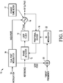
FIG. 1 illustrates, in block diagram form, a PLL in accordance with an embodiment. -
FIG. 2 illustrates a waveform diagram of low port and high port transfer functions for the dual port modulator ofFIG. 1 . -
FIG. 3 illustrates, in block diagram form, a high port modulation portion of the dual port modulator ofFIG. 1 in more detail. -
FIG. 4 illustrates, in block diagram form, the high port fractional modulator ofFIG. 3 in more detail. -
FIG. 5 illustrates, in block diagram form, the various signals provided to the voltage controlled oscillator ofFIG. 1 in more detail. -
FIG. 6 illustrates a table of thermometric codes used to map signed high port fractional modulator values to a discrete set of LSB varactors. - Generally, there is provided, a PLL with dual port modulation. In the dual port modulation, an input modulation signal is split into a high port modulation portion and a low port modulation portion. The high port modulation having a high port integer portion and a high port modulation fractional portion. A high port fractional modulator includes a sigma-delta modulator for providing the high port fractional portion. The sigma-delta modulator has a single signed-bit output. The single signed bit output is coupled to a binary-to-thermometric converter. The binary-to-thermometric converter is used for tuning a bank of varactors in a VCO of the PLL. Using a sigma-delta modulator with a single signed-bit output coupled to a binary-to-thermometric converter reduces spurious content due to VCO varactor and signal routing mismatches. Also, to mitigate idle tones that can occur in modulation if a long string of ones or zeros are modulated, a dithering circuit may be implemented with the sigma-delta modulator.
- In one embodiment, there is provided, an integrated circuit comprising: a dual port modulator having a first input for receiving a transmitter modulation signal, a first output for providing a fractional portion of a high port modulation signal, a second output for providing an integer portion of the high port modulation signal, and a third output for providing a low port modulation signal; a voltage controlled oscillator (VCO) coupled to the dual port modulator, the VCO having a first input for receiving the fractional portion of the high port modulation signal, a second input for receiving the integer portion of the high port modulation signal, a third input for receiving a tuning signal based on the low port modulation signal, and a first output for outputting an RF signal; and wherein a signed single bit signal is used for generating the fractional portion of the high port modulation signal. The fractional portion of the high port modulation signal may be applied to the VCO at a higher clock rate than the integer portion of the high port modulation signal. The dual port modulator may comprise a high port fractional modulator for producing the signed single bit signal used for generating the fractional portion of the high port modulation signal. The dual port modulator may further comprise an integer fraction splitter circuit for receiving the high port modulation signal, for providing a first signal to the high port fractional modulator for generating the fractional portion of the high port modulation signal, and for providing a second signal for generating the integer portion of the high port modulation signal. The dual port modulator may further comprise a binary to thermometric converter coupled to the high port fractional modulator for converting the signed single bit signal into a thermometric digital code for producing the high port modulation signal. The high port fractional modulator may comprise a second order or higher sigma-delta modulator. The high port fractional modulator may further comprise a quantizer coupled to the second order or higher sigma-delta modulator for producing the signed single bit signal. The integrated circuit may further comprise a zero-mean dithering circuit coupled to the second order or higher sigma-delta modulator for mitigating idle tones in modulation. The signed single bit signal of the quantizer may provide three signed states which are mapped to two thermometric varactors in the VCO.
- In another embodiment, there is provided, a method of modulation comprising: receiving a fractional portion of a high port modulation signal at a first input of a voltage controlled oscillator (VCO), the fractional portion of the high port modulation signal based on a signed single bit signal; receiving an integer portion of the high port modulation signal at a second input of the VCO; receiving a VCO tuning signal at a third input of the VCO; and generating an RF signal at an output of the VCO. The method may further comprise generating the fractional portion of a high port modulation signal at a first output of a dual port modulator and generating the integer portion of the high port modulation signal at a second output of the dual port modulator. The method may further comprise generating, with an integer fraction splitter receiving the high port modulation signal, a first output signal and a second output signal based on the high port modulation signal. The method may further comprise receiving the first output signal at a high port fractional modulator, the high port fractional modulator generating the signed single bit signal. The method may further comprise receiving the signed single bit signal at a binary-to-thermometer code converter, and converting the signed single bit signal to a thermometric coded signal, the thermometric coded signal being characterized as the fractional portion of the high port modulation signal and provided to the first input of the VCO. The method may further comprise generating the high port modulation signal by mixing a transmitter modulation signal with a calibration signal. The method may further comprise generating the integer portion of the high port modulation signal by delaying the second output signal such that the integer portion of the high port modulation signal is aligned with the fractional portion of the high port modulation signal. The step of receiving the first output signal at a high port fractional modulator may comprise dithering the first output signal. The method may further comprise generating a low port modulation signal with a sigma delta modulator, the sigma delta modulator receiving a signal comprising mixing a target frequency signal with a low port signal output at a third output of the dual port modulator, the tuning signal being based on the low port modulation signal.
- In yet another embodiment, there is provided, an integrated circuit comprising: a voltage controlled oscillator (VCO) for generating an RF signal, the VCO having a first input for receiving a fractional portion of a high port modulation signal, a second input for receiving an integer portion of the high port modulation signal, a third input for receiving a tuning signal; and a dual port modulator coupled to the VCO, the dual port modulator for receiving a transmitter modulation signal and for providing modulation signals to the VCO, the dual port modulator receiving the transmitter modulation signal at a first input, providing at a first output the fractional portion of the high port modulation signal based on a signed single bit signal, providing the integer portion of the high port modulation signal at a second output, and providing a low port modulation signal at a third output; and wherein the fractional portion of the high port modulation signal is based on a signed single bit signal. The tuning signal may be based on a low port modulation signal.
-
FIG. 1 illustrates, in block diagram form, aPLL 10 in accordance with an embodiment. Phase lockedloop 10 includesphase detector 12,loop filter 14,VCO 16,coarse tune block 17,fractional divider 18,adder 20, sigma-delta modulator 22, anddual port modulator 24.Phase detector 12 has a first input for receiving a reference clock signal labeled "REFERENCE", a second input for receiving a feedback signal fromfractional divider 18, and an output coupled to an input ofloop filter 14. Voltage controlledoscillator 16 has a first input coupled to an output ofloop filter 14 for receiving a VCO tuning signal labeled "VTUNE", a second input coupled to an output ofdual port modulator 24 for receiving a high port modulation tuning signal labeled "HIGH PORT", and an output for providing an RF output signal labeled "RF OUTPUT".Fractional divider 18 has an input coupled to the output ofVCO 16, and an output coupled to the second input ofphase detector 12.Adder 20 has a first input coupled to receive a frequency band selection signal labeled "TARGET FREQUENCY", a second input coupled to an output ofdual port modulator 24, and an output coupled to an input of sigma-delta modulator 22. Sigma-delta modulator 22 has an output coupled to an input offractional divider 18.Dual port modulator 24 has an input coupled to receive a transmit modulation signal labeled "TX MODULATION". Note thatFIG. 1 provides a simplified view of the circuit blocks that make upPLL 10. With respect toVCO 16, additional signals will be illustrated inFIG. 5 that are not shown inFIG. 1 . - In the illustrated embodiment,
PLL 10 includes both digital and analog circuitry. In other embodiments,PLL 10 may be characterized as either an analog PLL or a digital PLL and the concepts discussed herein will be equally applicable to both. Generally,PLL 10 operates as a conventional PLL. That is, a feedback signal is compared to a reference frequency signal inphase detector 12. In response,phase detector 12 provides a control voltage for adjusting the output frequency ofVCO 16 after being filtered byloop filter 14, and provided byloop filter 14 as VCO tuning signal VTUNE. A VCO band selection signal fromcoarse tune block 17 is provided as a separate input which is applied to an open loop VCO to drive the RF output frequency close to (within a few megahertz) of the TARGET FREQUENCY. Voltage controlledoscillator 16 also receives tuning signal HIGH PORT fromdual port modulator 24. In addition,dual port modulator 24 provides tuning signal LOW PORT to adder 20.Adder 20 combines tuning signal LOW PORT with the desired PLL frequency given by TARGET FREQUENCY and provides the resulting output to adjust sigma-delta modulator 22 for the selected frequency band. Sigma-delta modulator 22 provides a signal for settingfractional divider 18 for the selected frequency band. Together tuning signals VTUNE and HIGH PORT adjust the output frequency of output signal RF OUTPUT. The adjusted output signal RF OUTPUT is fed back tophase detector 12 throughfractional divider 18. In one embodiment,fractional divider 18 is a programmable multi-modulus divider controlled by sigma-delta modulator 22. Using fractional divide values provides a PLL with higher resolution. In one embodiment, sigma-delta modulator is characterized as being a third-order sigma-delta modulator. In other embodiments, sigma-delta modulator 22 may be a different type of fractional modulator. - In one embodiment,
VCO 16 can be implemented as a conventional negative transconductance metal-oxide semiconductor (MOS) inductive-capacitive (LC) oscillator circuit. The LC oscillator includes one or more banks, or arrays, of varactors (variable reactors) for tuningVCO 16 with respect to frequency (not shown). In one embodiment, a varactor in a bank of varactors is implemented as a capacitor and a switch. In another embodiment, a variable capacitance of a varactor is controlled using a control voltage. Alternately, a varactor may be implemented differently. In accordance with the described embodiment, a size, or capacitance value, of each varactor in a bank of varactors is based on a binary weighting, or bit position in the bank. For example, a least significant bit (LSB) position would have a smaller, or smallest, sized capacitor, and a most significant bit (MSB) position would have a larger, or largest, sized capacitor. In another embodiment, all of the varactors in a bank may be sized similarly. In yet another embodiment, the change in capacitance is a function of a change in the control voltage supplied to a single varactor. -
FIG. 2 illustrates a waveform diagram of low port and high port transfer functions for the dual port modulator ofFIG. 1 . The waveform illustrates the transfer function magnitudes versus frequency. InFIG. 2 , the high port transfer function is shown by the single dashed line. The low port transfer function is represented using the solid line. The frequency modulation limit due to sampling frequency is represented by the double dashed line. The composite modulation transfer function is a composite of the low port transfer function and the high port transfer function and is illustrated as a horizontal straight line. -
FIG. 3 illustrates, in block diagram form, a high port modulation portion of the dual port modulator ofFIG. 1 in more detail.Dual port modulator 24 includesmultiplier 30,PLL calibration block 32,integer fraction splitter 34, high portfractional modulator 36,delay 38, and binary-to-thermometer converter 40.Multiplier 30 has a first input for receiving input signal TX MODULATION, a second input for receiving a scaling signal labeled "HIGH PORT SCALE", and an output for providing a high port modulation signal labeled "HIGH PORT MODULATION". A hashed connection inFIG. 3 indicates that the value being conducted between blocks has multiple bits. An arrowhead indicates the direction the value is transmitted. An "s" by the hash mark indicates that the value is signed, and a "u" by the hash mark indicates that the value is unsigned. Also, a variable "p" indicates that the conducted value has p integer bits, and a variable "q" indicates the conducted value has q fractional bits. For example, a connection labeled with a "sp.q" indicates a signed value with p integer bits and q fractional bits.Integer fraction splitter 34 has an input for receiving the HIGH PORT MODULATION signal, a first output coupled to an input of high portfractional modulator 36, and a second output coupled to an input ofdelay 38.Delay 38 has an output for providing an integer portion of HIGH PORT MODULATION signal labeled "HIGH PORT INTEGER". Binary-to-thermometer converter 40 has an input coupled to the output of high portfractional modulator 36, and an output for providing a fractional portion of HIGH PORT MODULATION signal labeled "HIGH PORT FRACTION". High portfractional modulator 36 performs fractional modulation using a digital 2nd-order multi-bit MASH sigma-delta modulator, which converts a multi-bit binary fractional part to three signed single-bit states (-1, 0, +1). These signed states are mapped to two thermometric LSB varactors (not shown).FIG. 6 illustrates a table of unsigned two-bit thermometric output codes that correspond to the signed one-bit high port fractional modulator input values. Together, HIGH PORT INTEGER value provided bydelay 38 and HIGH PORT FRACTION value provided by converter 42 comprise the complete HIGH PORT signal illustrated inFIG. 1 . In an alternate configuration, the signed p bit (Sp) of the HIGH PORT INTEGER signal might need to be processed by an encoding stage if the high port integer bank has been realized using a hybrid or segmented architecture. - The HIGH PORT FRACTION value is used to drive a high port modulation bank of varactors in
VCO 16 ofFIG. 1 as describe above with reference to an LC oscillator having varactor banks. In one embodiment, the high port bank of varactors is a plurality of very finely quantized digitally switchable varactors with a capacitance in atto-Farads and a frequency resolution in kilo Hertz. The high port modulation includes an integer bank (either thermometric, binary addressable, or segmented) and a set of LSB (least significant bit) varactors (not shown) for sigma-delta modulation. Integer modulation by, for example, a variable p, turns on an equivalent number of LSB varactors for a sample input time period determined by a reference clock. Fractional modulation is applied at a higher clock rate and turns on an LSB size varactor for part of the reference clock time period, such that the time average over the reference clock period equals the fractional value. In one embodiment, the higher clock rate of the fractional modulation is two times higher than the reference clock rate. -
FIG. 4 illustrates, in block diagram form, the high portfractional modulator 36 ofFIG. 3 in more detail. High portfractional modulator 36 includes adither circuit 48 and a second order sigma-delta modulator 49. The high port fractional modulation applies a scaling to the PLL frequency modulation command that maps the instantaneous digital frequency modulation command with low port modulation sigma-delta LSB resolution to the high port modulation varactor bank LSB size.Dither circuit 48 includesmapping circuit 52, linear feedback shift register (LFSR) 50, scalingcircuit 54, andsummation circuit 56. In ditheringcircuit 48,LFSR 50 has an output coupled to an input ofmapping circuit 52.Mapping circuit 52 has an output coupled to an input of scalingcircuit 54.Mapping circuit 52 provides a unipolar to bipolar transformation of the output fromLFSR 50.Scaling circuit 54 has an output coupled to an input ofsummation circuit 56 for providing a dithering component to be summed with the signal from integer fraction splitter 34 (FIG. 3 ) to improve spectral characteristics offractional modulator 36. If enabled, dithering is continuously applied, whether the modulation data is varying or comprised of either a string of zeros or a string of ones. Dithering is accomplished by adding a long LFSR sequence (e.g. 17 bits or more, chosen as a function of the dither clock (not shown) and a set of varying or repeating modulation symbols) to the sigma-delta modulation input. Using LFSR based sigma-delta dithering essentially introduces an additive randomized insignificant magnitude modulation to the sigma-delta input. The dithering avoids modulation path idle tones due to a string of the same modulation symbol being transmitted by introducing a randomized dither that is added to the fractional sigma-delta modulator 49. The dithering is insignificant enough to not cause spectral degradation of PLL modulation. Other embodiments may not include dithering as provided bydither circuit 48. -
Modulator 36 includesaccumulators summation circuits circuits quantizer 76.Accumulator 58 has a first input coupled to the output ofsummation circuit 56, a second input, and an output.Accumulator 60 has a first input coupled to the output ofaccumulator 58, a second input, and an output.Summation circuit 62 has a first input coupled to the output ofaccumulator 58, a second input, and an output coupled to the second input ofaccumulator 58.Summation circuit 64 has a first input coupled to the output ofaccumulator 60, a second input, and an output coupled to the second input ofaccumulator 60.Scaling circuit 66 has an input coupled to an output ofquantizer 76, and an output coupled to the second input ofsummation circuit 62.Scaling circuit 68 has an input coupled to the output ofquantizer 76, and an output coupled to the second input ofsummation circuit 64.Scaling circuits modulator 36 can receive.Scaling circuit 72 has an input coupled to the output ofaccumulator 58, and an output.Scaling circuit 74 has an input coupled to the output ofaccumulator 60, and an output. In the illustrated embodiment, scalingcircuits Summation circuit 70 has a first input coupled to the output of scalingcircuit 72, a second input coupled to the output of scalingcircuit 74, and an output. The output ofsummation circuit 70 has multiple bits.Quantizer 76 has an input coupled to the output ofsummation circuit 70, and an output coupled to the input of binary-to-thermometer converter 40 (FIG. 3 ).Quantizer 76 converts the multiple bit output signal fromsummation circuit 70 to a single signed value. In the illustrated embodiment, the output ofquantizer 76 is either -1, 0, or +1. For most of the time, the output ofquantizer 76 changes by 1 state or less, which removes a number of physical sigma-delta implementation artifacts caused by size, delay skew, and a possible mismatch between rise and fall times between a multiple bit sigma-delta output. The sigma-delta output range is symmetric and does not introduce a bias in the dithered fractional value. Note that although a second order sigma-delta modulator is described, one skilled in the art will be able to extend the described approach to higher order sigma-delta modulators. -
FIG. 5 illustrates, in block diagram form, the various signals provided to the voltage controlled oscillator ofFIG. 1 in more detail.VCO 16 has an input for receiving a VCO tuning signal labeled "VTUNE", an input for receiving a coarse tuning signal labeled "COARSE TUNE", an input for receiving the HIGH PORT INTEGER value fromdelay 38 illustrated inFIG. 3 , an input for receiving the HIGH PORT FRACTION value illustrated inFIG. 3 , and an output labeled "RF OUTPUT".VCO 16 includes one or more banks ofvaractors 17. -
FIG. 6 illustrates a table of thermometric codes used to map signed high port fractional modulator values to a discrete set of LSB varactors. The high port fractional modulator output is determined by VCO frequency and may change in response to frequency changes when the VCO is, for example, locked. During PLL wake-up and operation in the absence of modulation, the fractional modulator output is 0, which is mapped to having one LSB varactor permanently enabled. When a fractional modulation of the high port modulator bank is enabled, the fractional modulator can have three signed states, where the frequency can either go up, stay the same, or go down. For example, if the VCO frequency is not changing, the high port fractional modulator output provides a fixed signed single-bit value such as 0, and the binary-to-thermometer converter will convert the 0 to an unsigned two-bit value 01 (or10) as illustrated in the second row of the table ofFIG. 6 . If the modulation reduces the VCO frequency by a fractional amount of one LSB frequency step, the output may be -1 with a corresponding thermometric code of 00 (first row). If the modulation increases VCO frequency changes by a fractional amount of one LSB frequency step, the fractional modulator output may be +1 with a corresponding thermometric code of 11 (i.e., two LSB frequency steps as illustrated in the third row). In other embodiments, the values in the table may be different and may be a function of the specific VCO implementation. That is, the mapping may depend on the type of devices used and how the devices that comprise the modulation tank circuit are connected together. For example, the binary-to-thermometer converter may convert the -1 to an unsigned two-bit value 11, the 0 may convert to 01 or 10, and the +1 may convert to 00. Note that a signed single-bit signal is equivalent to an unsigned 2-bit signal and in this case has three states (-1, 0, +1).
Using a sigma-delta modulator with a single signed-bit output coupled to a binary-to-thermometric converter as described above reduces spurious content due to VCO varactor and signal routing mismatches. - Because the apparatus implementing the present invention is, for the most part, composed of electronic components and circuits known to those skilled in the art, circuit details will not be explained in any greater extent than that considered necessary as illustrated above, for the understanding and appreciation of the underlying concepts of the present invention and in order not to obfuscate or distract from the teachings of the present invention. Although the invention is described herein with reference to specific embodiments, various modifications and changes can be made without departing from the scope of the present invention as set forth in the claims below. Accordingly, the specification and figures are to be regarded in an illustrative rather than a restrictive sense, and all such modifications are intended to be included within the scope of the present invention. Any benefits, advantages, or solutions to problems that are described herein with regard to specific embodiments are not intended to be construed as a critical, required, or essential feature or element of any or all the claims.
- The term "coupled," as used herein, is not intended to be limited to a direct coupling or a mechanical coupling.
- Furthermore, the terms "a" or "an," as used herein, are defined as one or more than one. Also, the use of introductory phrases such as "at least one" and "one or more" in the claims should not be construed to imply that the introduction of another claim element by the indefinite articles "a" or "an" limits any particular claim containing such introduced claim element to inventions containing only one such element, even when the same claim includes the introductory phrases "one or more" or "at least one" and indefinite articles such as "a" or "an." The same holds true for the use of definite articles.
- Unless stated otherwise, terms such as "first" and "second" are used to arbitrarily distinguish between the elements such terms describe. Thus, these terms are not necessarily intended to indicate temporal or other prioritization of such elements.
Claims (15)
- An integrated circuit comprising:a dual port modulator (24) having a first input for receiving a transmitter modulation signal (TX MODULATION), a first output for providing a fractional portion of a high port modulation signal (HIGH PORT FRACTION), a second output for providing an integer portion of the high port modulation signal (HIGH PORT INTEGER), and a third output for providing a low port modulation signal (LOW PORT);a voltage controlled oscillator (VCO) (16) coupled to the dual port modulator, the VCO having a first input for receiving the fractional portion of the high port modulation signal, a second input for receiving the integer portion of the high port modulation signal, a third input for receiving a tuning signal (VTUNE) based on the low port modulation signal, and a first output for outputting an RF signal (RF OUTPUT); andwherein a signed single bit signal (s1) is used for generating the fractional portion of the high port modulation signal.
- The integrated circuit of claim 1, wherein the fractional portion of the high port modulation signal is applied to the VCO at a higher clock rate than the integer portion of the high port modulation signal.
- The integrated circuit of claim 1 or 2, wherein the dual port modulator comprises a high port fractional modulator (36) for producing the signed single bit signal used for generating the fractional portion of the high port modulation signal.
- The integrated circuit of claim 3, wherein the dual port modulator further comprises an integer fraction splitter circuit (34) for receiving the high port modulation signal, for providing a first signal to the high port fractional modulator for generating the fractional portion of the high port modulation signal, and for providing a second signal for generating the integer portion of the high port modulation signal.
- The integrated circuit of claim 3 or 4, wherein the dual port modulator further comprises a binary to thermometric converter (40) coupled to the high port fractional modulator for converting the signed single bit signal into a thermometric digital code for producing the high port modulation signal.
- The integrated circuit of any of claims 3 to 5, wherein the high port fractional modulator comprises a second order or higher sigma-delta modulator.
- The integrated circuit of claim 6, wherein the high port fractional modulator further comprises a quantizer (76) coupled to the second order or higher sigma-delta modulator for producing the signed single bit signal.
- The integrated circuit of claim 6 or 7, further comprising a zero-mean dithering circuit coupled to the second order or higher sigma-delta modulator for mitigating idle tones in modulation.
- The integrated circuit of claim 7, wherein the signed single bit signal of the quantizer provides three signed states which are mapped to two thermometric varactors in the VCO.
- A method of modulation comprising:receiving a fractional portion of a high port modulation signal (HIGH PORT FRACTION) at a first input of a voltage controlled oscillator (VCO) (16), the fractional portion of the high port modulation signal based on a signed single bit signal (s1);receiving an integer portion of the high port modulation signal (HIGH PORT INTEGER) at a second input of the VCO;receiving a VCO tuning signal (VTUNE) at a third input of the VCO; andgenerating an RF signal (RF OUTPUT) at an output of the VCO.
- The method of claim 10, further comprising generating the fractional portion of a high port modulation signal at a first output of a dual port modulator (24) and generating the integer portion of the high port modulation signal at a second output of the dual port modulator.
- The method of claim 10 or 11, further comprising generating, with an integer fraction splitter (34) receiving the high port modulation signal, a first output signal and a second output signal based on the high port modulation signal.
- The method of claim12, further comprising receiving the first output signal at a high port fractional modulator (36), the high port fractional modulator generating the signed single bit signal.
- The method of claim 13, further comprising receiving the signed single bit signal at a binary-to-thermometer code converter (40), and converting the signed single bit signal to a thermometric coded signal, the thermometric coded signal being characterized as the fractional portion of the high port modulation signal and provided to the first input of the VCO.
- The method of any of claims 12 to 14, further comprising generating the high port modulation signal by mixing (30) a transmitter modulation signal with a calibration signal.
Applications Claiming Priority (1)
| Application Number | Priority Date | Filing Date | Title |
|---|---|---|---|
| US14/631,305 US9484936B2 (en) | 2015-02-25 | 2015-02-25 | Phase locked loop having fractional VCO modulation |
Publications (2)
| Publication Number | Publication Date |
|---|---|
| EP3062444A1 true EP3062444A1 (en) | 2016-08-31 |
| EP3062444B1 EP3062444B1 (en) | 2018-07-04 |
Family
ID=55345741
Family Applications (1)
| Application Number | Title | Priority Date | Filing Date |
|---|---|---|---|
| EP16155022.3A Active EP3062444B1 (en) | 2015-02-25 | 2016-02-10 | Phase locked loop having fractional vco modulation |
Country Status (3)
| Country | Link |
|---|---|
| US (1) | US9484936B2 (en) |
| EP (1) | EP3062444B1 (en) |
| CN (1) | CN105915212B (en) |
Families Citing this family (8)
| Publication number | Priority date | Publication date | Assignee | Title |
|---|---|---|---|---|
| US10623008B2 (en) * | 2015-04-30 | 2020-04-14 | Xilinx, Inc. | Reconfigurable fractional-N frequency generation for a phase-locked loop |
| EP3343773B1 (en) * | 2016-12-29 | 2022-06-01 | Nxp B.V. | Chirp generator using a pll |
| US10236899B1 (en) * | 2018-02-22 | 2019-03-19 | Allegro Microsystems, Llc | Tunable fractional phase locked loop |
| US10715151B2 (en) | 2018-03-22 | 2020-07-14 | Qualcomm Incorporated | Fast coarse tuning for frequency synthesizer |
| US10348310B1 (en) * | 2018-05-30 | 2019-07-09 | Xilinx, Inc. | Programmable digital sigma delta modulator |
| CN111010173B (en) * | 2019-12-20 | 2023-05-23 | 湖北大学 | An adaptive fractional frequency synthesizer glitch removal system and method |
| CN111900978B (en) * | 2020-08-07 | 2021-11-23 | 上海橙群微电子有限公司 | Phase-locked loop circuit, transmitter and wireless transceiving system |
| EP4064568B1 (en) * | 2021-03-23 | 2025-05-07 | Nxp B.V. | Type-i plls for phase-controlled applications |
Citations (4)
| Publication number | Priority date | Publication date | Assignee | Title |
|---|---|---|---|---|
| US20060170511A1 (en) * | 2005-01-28 | 2006-08-03 | Dunworth Jeremy D | Coarse frequency tuning in a voltage controlled oscillator |
| US20070035354A1 (en) * | 2005-08-15 | 2007-02-15 | Chan Evelyn L | Dual port modulator |
| US20090195275A1 (en) * | 2008-02-01 | 2009-08-06 | Daniel Joseph Friedman | Technique for efficiently managing both short-term and long-term frequency adjustments of an electronic circuit clock signal |
| US20100231310A1 (en) * | 2009-03-16 | 2010-09-16 | Mediatek Inc. | Mixed-mode pll |
Family Cites Families (13)
| Publication number | Priority date | Publication date | Assignee | Title |
|---|---|---|---|---|
| US6294936B1 (en) | 1998-09-28 | 2001-09-25 | American Microsystems, Inc. | Spread-spectrum modulation methods and circuit for clock generator phase-locked loop |
| US7046098B2 (en) | 2001-11-27 | 2006-05-16 | Texas Instruments Incorporated | All-digital frequency synthesis with capacitive re-introduction of dithered tuning information |
| US6823033B2 (en) | 2002-03-12 | 2004-11-23 | Qualcomm Inc. | ΣΔdelta modulator controlled phase locked loop with a noise shaped dither |
| US6856791B2 (en) | 2002-03-14 | 2005-02-15 | Ericsson Inc. | Direct automatic frequency control method and apparatus |
| US7439817B2 (en) | 2006-02-16 | 2008-10-21 | Texas Instruments Incorporated | Frequency tuning range extension and modulation resolution enhancement of a digitally controlled oscillator |
| US7570182B2 (en) | 2006-09-15 | 2009-08-04 | Texas Instruments Incorporated | Adaptive spectral noise shaping to improve time to digital converter quantization resolution using dithering |
| US8045670B2 (en) | 2007-06-22 | 2011-10-25 | Texas Instruments Incorporated | Interpolative all-digital phase locked loop |
| US8045669B2 (en) * | 2007-11-29 | 2011-10-25 | Qualcomm Incorporated | Digital phase-locked loop operating based on fractional input and output phases |
| US7843730B2 (en) | 2008-01-16 | 2010-11-30 | Freescale Semiconductor, Inc. | Non-volatile memory with reduced charge fluence |
| US7772900B2 (en) | 2008-07-15 | 2010-08-10 | International Business Machines Corporation | Phase-locked loop circuits and methods implementing pulsewidth modulation for fine tuning control of digitally controlled oscillators |
| WO2010092438A1 (en) * | 2009-02-13 | 2010-08-19 | Freescale Semiconductor, Inc. | Integrated circuit comprising frequency generation circuitry for controlling a frequency source |
| US8378751B2 (en) * | 2009-02-13 | 2013-02-19 | Qualcomm Incorporated | Frequency synthesizer with multiple tuning loops |
| US8536916B1 (en) | 2011-09-12 | 2013-09-17 | Entropic Communications, Inc. | Digitally controlled oscillator with thermometer sigma delta encoded frequency control word |
-
2015
- 2015-02-25 US US14/631,305 patent/US9484936B2/en active Active
-
2016
- 2016-01-28 CN CN201610056780.0A patent/CN105915212B/en active Active
- 2016-02-10 EP EP16155022.3A patent/EP3062444B1/en active Active
Patent Citations (4)
| Publication number | Priority date | Publication date | Assignee | Title |
|---|---|---|---|---|
| US20060170511A1 (en) * | 2005-01-28 | 2006-08-03 | Dunworth Jeremy D | Coarse frequency tuning in a voltage controlled oscillator |
| US20070035354A1 (en) * | 2005-08-15 | 2007-02-15 | Chan Evelyn L | Dual port modulator |
| US20090195275A1 (en) * | 2008-02-01 | 2009-08-06 | Daniel Joseph Friedman | Technique for efficiently managing both short-term and long-term frequency adjustments of an electronic circuit clock signal |
| US20100231310A1 (en) * | 2009-03-16 | 2010-09-16 | Mediatek Inc. | Mixed-mode pll |
Also Published As
| Publication number | Publication date |
|---|---|
| US9484936B2 (en) | 2016-11-01 |
| EP3062444B1 (en) | 2018-07-04 |
| CN105915212B (en) | 2020-11-06 |
| US20160248430A1 (en) | 2016-08-25 |
| CN105915212A (en) | 2016-08-31 |
Similar Documents
| Publication | Publication Date | Title |
|---|---|---|
| EP3062444B1 (en) | Phase locked loop having fractional vco modulation | |
| US9300307B2 (en) | Arbitrary phase trajectory frequency synthesizer | |
| US6646581B1 (en) | Digital-to-analog converter circuit incorporating hybrid sigma-delta modulator circuit | |
| US7084710B2 (en) | Digital expander apparatus and method for generating multiple analog control signals particularly useful for controlling an oscillator | |
| US9397675B1 (en) | Hybrid frequency synthesizer and method | |
| US9154143B2 (en) | Semiconductor device | |
| US8193845B2 (en) | Binary-weighted delta-sigma fractional-N frequency synthesizer with digital-to-analog differentiators canceling quantization noise | |
| US20030043950A1 (en) | Phase-locked loop frequency synthesizer with two-point modulation | |
| US7605665B2 (en) | Fractional-N phase locked loop | |
| EP2673931A1 (en) | Two point modulation digital phase locked loop | |
| WO2004088846A1 (en) | Method and system of jitter compensation | |
| EP3888246B1 (en) | Fractional frequency synthesis by sigma-delta modulating frequency of a reference clock | |
| WO2001011783A1 (en) | Fractional- n frequency synthesiser | |
| JP2012039551A (en) | Pll frequency synthesizer, radio communication device, and control method of pll frequency synthesizer | |
| JP4275502B2 (en) | Fractional N frequency synthesizer and fractional N frequency synthesizer method | |
| CN105763187A (en) | Modulator and time delay automatic calibration circuit and time delay control module thereof | |
| US7719369B2 (en) | Sigma delta digital to analog converter with wide output range and improved linearity | |
| Su et al. | A 2.4 GHz wideband open-loop GFSK transmitter with phase quantization noise cancellation | |
| CA2370254A1 (en) | Improvements relating to frequency synthesisers | |
| US10374618B1 (en) | Frequency locked loop with multi-bit sampler | |
| CN110690899B (en) | Gain calibration method and module of high-pass path in two-point modulation phase-locked loop | |
| US12057845B2 (en) | Fractional divider-calibrated phase modulator and interpolator for a wireless transmitter | |
| Lee et al. | A fractional-N frequency synthesizer with a 3-bit 4 th order Σ-Δ modulator | |
| Sotiriadis et al. | Single-bit all digital frequency synthesis with homodyne sigma-delta modulation for Internet of Things applications | |
| Nidhi et al. | Open‐Loop Wide‐Bandwidth Phase Modulation Techniques |
Legal Events
| Date | Code | Title | Description |
|---|---|---|---|
| PUAI | Public reference made under article 153(3) epc to a published international application that has entered the european phase |
Free format text: ORIGINAL CODE: 0009012 |
|
| AK | Designated contracting states |
Kind code of ref document: A1 Designated state(s): AL AT BE BG CH CY CZ DE DK EE ES FI FR GB GR HR HU IE IS IT LI LT LU LV MC MK MT NL NO PL PT RO RS SE SI SK SM TR |
|
| AX | Request for extension of the european patent |
Extension state: BA ME |
|
| RAP1 | Party data changed (applicant data changed or rights of an application transferred) |
Owner name: NXP USA, INC. |
|
| STAA | Information on the status of an ep patent application or granted ep patent |
Free format text: STATUS: REQUEST FOR EXAMINATION WAS MADE |
|
| 17P | Request for examination filed |
Effective date: 20170228 |
|
| RBV | Designated contracting states (corrected) |
Designated state(s): AL AT BE BG CH CY CZ DE DK EE ES FI FR GB GR HR HU IE IS IT LI LT LU LV MC MK MT NL NO PL PT RO RS SE SI SK SM TR |
|
| GRAP | Despatch of communication of intention to grant a patent |
Free format text: ORIGINAL CODE: EPIDOSNIGR1 |
|
| STAA | Information on the status of an ep patent application or granted ep patent |
Free format text: STATUS: GRANT OF PATENT IS INTENDED |
|
| INTG | Intention to grant announced |
Effective date: 20180119 |
|
| INTG | Intention to grant announced |
Effective date: 20180119 |
|
| GRAS | Grant fee paid |
Free format text: ORIGINAL CODE: EPIDOSNIGR3 |
|
| GRAA | (expected) grant |
Free format text: ORIGINAL CODE: 0009210 |
|
| STAA | Information on the status of an ep patent application or granted ep patent |
Free format text: STATUS: THE PATENT HAS BEEN GRANTED |
|
| AK | Designated contracting states |
Kind code of ref document: B1 Designated state(s): AL AT BE BG CH CY CZ DE DK EE ES FI FR GB GR HR HU IE IS IT LI LT LU LV MC MK MT NL NO PL PT RO RS SE SI SK SM TR |
|
| REG | Reference to a national code |
Ref country code: GB Ref legal event code: FG4D |
|
| REG | Reference to a national code |
Ref country code: CH Ref legal event code: EP |
|
| REG | Reference to a national code |
Ref country code: AT Ref legal event code: REF Ref document number: 1015593 Country of ref document: AT Kind code of ref document: T Effective date: 20180715 |
|
| REG | Reference to a national code |
Ref country code: IE Ref legal event code: FG4D |
|
| REG | Reference to a national code |
Ref country code: DE Ref legal event code: R096 Ref document number: 602016003870 Country of ref document: DE |
|
| REG | Reference to a national code |
Ref country code: NL Ref legal event code: MP Effective date: 20180704 |
|
| REG | Reference to a national code |
Ref country code: LT Ref legal event code: MG4D |
|
| REG | Reference to a national code |
Ref country code: AT Ref legal event code: MK05 Ref document number: 1015593 Country of ref document: AT Kind code of ref document: T Effective date: 20180704 |
|
| PG25 | Lapsed in a contracting state [announced via postgrant information from national office to epo] |
Ref country code: NL Free format text: LAPSE BECAUSE OF FAILURE TO SUBMIT A TRANSLATION OF THE DESCRIPTION OR TO PAY THE FEE WITHIN THE PRESCRIBED TIME-LIMIT Effective date: 20180704 |
|
| PG25 | Lapsed in a contracting state [announced via postgrant information from national office to epo] |
Ref country code: CZ Free format text: LAPSE BECAUSE OF FAILURE TO SUBMIT A TRANSLATION OF THE DESCRIPTION OR TO PAY THE FEE WITHIN THE PRESCRIBED TIME-LIMIT Effective date: 20180704 Ref country code: FI Free format text: LAPSE BECAUSE OF FAILURE TO SUBMIT A TRANSLATION OF THE DESCRIPTION OR TO PAY THE FEE WITHIN THE PRESCRIBED TIME-LIMIT Effective date: 20180704 Ref country code: IS Free format text: LAPSE BECAUSE OF FAILURE TO SUBMIT A TRANSLATION OF THE DESCRIPTION OR TO PAY THE FEE WITHIN THE PRESCRIBED TIME-LIMIT Effective date: 20181104 Ref country code: BG Free format text: LAPSE BECAUSE OF FAILURE TO SUBMIT A TRANSLATION OF THE DESCRIPTION OR TO PAY THE FEE WITHIN THE PRESCRIBED TIME-LIMIT Effective date: 20181004 Ref country code: SE Free format text: LAPSE BECAUSE OF FAILURE TO SUBMIT A TRANSLATION OF THE DESCRIPTION OR TO PAY THE FEE WITHIN THE PRESCRIBED TIME-LIMIT Effective date: 20180704 Ref country code: AT Free format text: LAPSE BECAUSE OF FAILURE TO SUBMIT A TRANSLATION OF THE DESCRIPTION OR TO PAY THE FEE WITHIN THE PRESCRIBED TIME-LIMIT Effective date: 20180704 Ref country code: NO Free format text: LAPSE BECAUSE OF FAILURE TO SUBMIT A TRANSLATION OF THE DESCRIPTION OR TO PAY THE FEE WITHIN THE PRESCRIBED TIME-LIMIT Effective date: 20181004 Ref country code: RS Free format text: LAPSE BECAUSE OF FAILURE TO SUBMIT A TRANSLATION OF THE DESCRIPTION OR TO PAY THE FEE WITHIN THE PRESCRIBED TIME-LIMIT Effective date: 20180704 Ref country code: LT Free format text: LAPSE BECAUSE OF FAILURE TO SUBMIT A TRANSLATION OF THE DESCRIPTION OR TO PAY THE FEE WITHIN THE PRESCRIBED TIME-LIMIT Effective date: 20180704 Ref country code: GR Free format text: LAPSE BECAUSE OF FAILURE TO SUBMIT A TRANSLATION OF THE DESCRIPTION OR TO PAY THE FEE WITHIN THE PRESCRIBED TIME-LIMIT Effective date: 20181005 Ref country code: PL Free format text: LAPSE BECAUSE OF FAILURE TO SUBMIT A TRANSLATION OF THE DESCRIPTION OR TO PAY THE FEE WITHIN THE PRESCRIBED TIME-LIMIT Effective date: 20180704 |
|
| PG25 | Lapsed in a contracting state [announced via postgrant information from national office to epo] |
Ref country code: ES Free format text: LAPSE BECAUSE OF FAILURE TO SUBMIT A TRANSLATION OF THE DESCRIPTION OR TO PAY THE FEE WITHIN THE PRESCRIBED TIME-LIMIT Effective date: 20180704 Ref country code: AL Free format text: LAPSE BECAUSE OF FAILURE TO SUBMIT A TRANSLATION OF THE DESCRIPTION OR TO PAY THE FEE WITHIN THE PRESCRIBED TIME-LIMIT Effective date: 20180704 Ref country code: LV Free format text: LAPSE BECAUSE OF FAILURE TO SUBMIT A TRANSLATION OF THE DESCRIPTION OR TO PAY THE FEE WITHIN THE PRESCRIBED TIME-LIMIT Effective date: 20180704 Ref country code: HR Free format text: LAPSE BECAUSE OF FAILURE TO SUBMIT A TRANSLATION OF THE DESCRIPTION OR TO PAY THE FEE WITHIN THE PRESCRIBED TIME-LIMIT Effective date: 20180704 |
|
| REG | Reference to a national code |
Ref country code: DE Ref legal event code: R097 Ref document number: 602016003870 Country of ref document: DE |
|
| PG25 | Lapsed in a contracting state [announced via postgrant information from national office to epo] |
Ref country code: IT Free format text: LAPSE BECAUSE OF FAILURE TO SUBMIT A TRANSLATION OF THE DESCRIPTION OR TO PAY THE FEE WITHIN THE PRESCRIBED TIME-LIMIT Effective date: 20180704 Ref country code: EE Free format text: LAPSE BECAUSE OF FAILURE TO SUBMIT A TRANSLATION OF THE DESCRIPTION OR TO PAY THE FEE WITHIN THE PRESCRIBED TIME-LIMIT Effective date: 20180704 Ref country code: RO Free format text: LAPSE BECAUSE OF FAILURE TO SUBMIT A TRANSLATION OF THE DESCRIPTION OR TO PAY THE FEE WITHIN THE PRESCRIBED TIME-LIMIT Effective date: 20180704 |
|
| PLBE | No opposition filed within time limit |
Free format text: ORIGINAL CODE: 0009261 |
|
| STAA | Information on the status of an ep patent application or granted ep patent |
Free format text: STATUS: NO OPPOSITION FILED WITHIN TIME LIMIT |
|
| PG25 | Lapsed in a contracting state [announced via postgrant information from national office to epo] |
Ref country code: SM Free format text: LAPSE BECAUSE OF FAILURE TO SUBMIT A TRANSLATION OF THE DESCRIPTION OR TO PAY THE FEE WITHIN THE PRESCRIBED TIME-LIMIT Effective date: 20180704 Ref country code: DK Free format text: LAPSE BECAUSE OF FAILURE TO SUBMIT A TRANSLATION OF THE DESCRIPTION OR TO PAY THE FEE WITHIN THE PRESCRIBED TIME-LIMIT Effective date: 20180704 Ref country code: SK Free format text: LAPSE BECAUSE OF FAILURE TO SUBMIT A TRANSLATION OF THE DESCRIPTION OR TO PAY THE FEE WITHIN THE PRESCRIBED TIME-LIMIT Effective date: 20180704 |
|
| 26N | No opposition filed |
Effective date: 20190405 |
|
| PG25 | Lapsed in a contracting state [announced via postgrant information from national office to epo] |
Ref country code: SI Free format text: LAPSE BECAUSE OF FAILURE TO SUBMIT A TRANSLATION OF THE DESCRIPTION OR TO PAY THE FEE WITHIN THE PRESCRIBED TIME-LIMIT Effective date: 20180704 |
|
| REG | Reference to a national code |
Ref country code: CH Ref legal event code: PL |
|
| PG25 | Lapsed in a contracting state [announced via postgrant information from national office to epo] |
Ref country code: MC Free format text: LAPSE BECAUSE OF FAILURE TO SUBMIT A TRANSLATION OF THE DESCRIPTION OR TO PAY THE FEE WITHIN THE PRESCRIBED TIME-LIMIT Effective date: 20180704 Ref country code: LU Free format text: LAPSE BECAUSE OF NON-PAYMENT OF DUE FEES Effective date: 20190210 |
|
| REG | Reference to a national code |
Ref country code: BE Ref legal event code: MM Effective date: 20190228 |
|
| REG | Reference to a national code |
Ref country code: IE Ref legal event code: MM4A |
|
| PG25 | Lapsed in a contracting state [announced via postgrant information from national office to epo] |
Ref country code: LI Free format text: LAPSE BECAUSE OF NON-PAYMENT OF DUE FEES Effective date: 20190228 Ref country code: CH Free format text: LAPSE BECAUSE OF NON-PAYMENT OF DUE FEES Effective date: 20190228 |
|
| PG25 | Lapsed in a contracting state [announced via postgrant information from national office to epo] |
Ref country code: IE Free format text: LAPSE BECAUSE OF NON-PAYMENT OF DUE FEES Effective date: 20190210 |
|
| PG25 | Lapsed in a contracting state [announced via postgrant information from national office to epo] |
Ref country code: BE Free format text: LAPSE BECAUSE OF NON-PAYMENT OF DUE FEES Effective date: 20190228 Ref country code: FR Free format text: LAPSE BECAUSE OF NON-PAYMENT OF DUE FEES Effective date: 20190228 |
|
| PG25 | Lapsed in a contracting state [announced via postgrant information from national office to epo] |
Ref country code: TR Free format text: LAPSE BECAUSE OF FAILURE TO SUBMIT A TRANSLATION OF THE DESCRIPTION OR TO PAY THE FEE WITHIN THE PRESCRIBED TIME-LIMIT Effective date: 20180704 |
|
| PG25 | Lapsed in a contracting state [announced via postgrant information from national office to epo] |
Ref country code: MT Free format text: LAPSE BECAUSE OF NON-PAYMENT OF DUE FEES Effective date: 20190210 Ref country code: PT Free format text: LAPSE BECAUSE OF FAILURE TO SUBMIT A TRANSLATION OF THE DESCRIPTION OR TO PAY THE FEE WITHIN THE PRESCRIBED TIME-LIMIT Effective date: 20181104 |
|
| GBPC | Gb: european patent ceased through non-payment of renewal fee |
Effective date: 20200210 |
|
| PG25 | Lapsed in a contracting state [announced via postgrant information from national office to epo] |
Ref country code: GB Free format text: LAPSE BECAUSE OF NON-PAYMENT OF DUE FEES Effective date: 20200210 |
|
| PG25 | Lapsed in a contracting state [announced via postgrant information from national office to epo] |
Ref country code: CY Free format text: LAPSE BECAUSE OF FAILURE TO SUBMIT A TRANSLATION OF THE DESCRIPTION OR TO PAY THE FEE WITHIN THE PRESCRIBED TIME-LIMIT Effective date: 20180704 |
|
| PG25 | Lapsed in a contracting state [announced via postgrant information from national office to epo] |
Ref country code: HU Free format text: LAPSE BECAUSE OF FAILURE TO SUBMIT A TRANSLATION OF THE DESCRIPTION OR TO PAY THE FEE WITHIN THE PRESCRIBED TIME-LIMIT; INVALID AB INITIO Effective date: 20160210 |
|
| PG25 | Lapsed in a contracting state [announced via postgrant information from national office to epo] |
Ref country code: MK Free format text: LAPSE BECAUSE OF FAILURE TO SUBMIT A TRANSLATION OF THE DESCRIPTION OR TO PAY THE FEE WITHIN THE PRESCRIBED TIME-LIMIT Effective date: 20180704 |
|
| P01 | Opt-out of the competence of the unified patent court (upc) registered |
Effective date: 20230725 |
|
| PGFP | Annual fee paid to national office [announced via postgrant information from national office to epo] |
Ref country code: DE Payment date: 20260121 Year of fee payment: 11 |