EP3062351A1 - Field-effect transistor - Google Patents
Field-effect transistor Download PDFInfo
- Publication number
- EP3062351A1 EP3062351A1 EP14854905.8A EP14854905A EP3062351A1 EP 3062351 A1 EP3062351 A1 EP 3062351A1 EP 14854905 A EP14854905 A EP 14854905A EP 3062351 A1 EP3062351 A1 EP 3062351A1
- Authority
- EP
- European Patent Office
- Prior art keywords
- effect transistor
- field
- dielectric constant
- type
- relative dielectric
- Prior art date
- Legal status (The legal status is an assumption and is not a legal conclusion. Google has not performed a legal analysis and makes no representation as to the accuracy of the status listed.)
- Granted
Links
Images







Classifications
-
- H—ELECTRICITY
- H10—SEMICONDUCTOR DEVICES; ELECTRIC SOLID-STATE DEVICES NOT OTHERWISE PROVIDED FOR
- H10D—INORGANIC ELECTRIC SEMICONDUCTOR DEVICES
- H10D64/00—Electrodes of devices having potential barriers
- H10D64/60—Electrodes characterised by their materials
- H10D64/66—Electrodes having a conductor capacitively coupled to a semiconductor by an insulator, e.g. MIS electrodes
- H10D64/68—Electrodes having a conductor capacitively coupled to a semiconductor by an insulator, e.g. MIS electrodes characterised by the insulator, e.g. by the gate insulator
- H10D64/681—Electrodes having a conductor capacitively coupled to a semiconductor by an insulator, e.g. MIS electrodes characterised by the insulator, e.g. by the gate insulator having a compositional variation, e.g. multilayered
- H10D64/685—Electrodes having a conductor capacitively coupled to a semiconductor by an insulator, e.g. MIS electrodes characterised by the insulator, e.g. by the gate insulator having a compositional variation, e.g. multilayered being perpendicular to the channel plane
-
- H—ELECTRICITY
- H10—SEMICONDUCTOR DEVICES; ELECTRIC SOLID-STATE DEVICES NOT OTHERWISE PROVIDED FOR
- H10D—INORGANIC ELECTRIC SEMICONDUCTOR DEVICES
- H10D30/00—Field-effect transistors [FET]
- H10D30/60—Insulated-gate field-effect transistors [IGFET]
-
- H—ELECTRICITY
- H10—SEMICONDUCTOR DEVICES; ELECTRIC SOLID-STATE DEVICES NOT OTHERWISE PROVIDED FOR
- H10D—INORGANIC ELECTRIC SEMICONDUCTOR DEVICES
- H10D30/00—Field-effect transistors [FET]
- H10D30/60—Insulated-gate field-effect transistors [IGFET]
- H10D30/67—Thin-film transistors [TFT]
- H10D30/6729—Thin-film transistors [TFT] characterised by the electrodes
- H10D30/6737—Thin-film transistors [TFT] characterised by the electrodes characterised by the electrode materials
- H10D30/6739—Conductor-insulator-semiconductor electrodes
-
- H—ELECTRICITY
- H10—SEMICONDUCTOR DEVICES; ELECTRIC SOLID-STATE DEVICES NOT OTHERWISE PROVIDED FOR
- H10D—INORGANIC ELECTRIC SEMICONDUCTOR DEVICES
- H10D30/00—Field-effect transistors [FET]
- H10D30/60—Insulated-gate field-effect transistors [IGFET]
- H10D30/67—Thin-film transistors [TFT]
- H10D30/674—Thin-film transistors [TFT] characterised by the active materials
- H10D30/6741—Group IV materials, e.g. germanium or silicon carbide
-
- H—ELECTRICITY
- H10—SEMICONDUCTOR DEVICES; ELECTRIC SOLID-STATE DEVICES NOT OTHERWISE PROVIDED FOR
- H10D—INORGANIC ELECTRIC SEMICONDUCTOR DEVICES
- H10D30/00—Field-effect transistors [FET]
- H10D30/60—Insulated-gate field-effect transistors [IGFET]
- H10D30/67—Thin-film transistors [TFT]
- H10D30/674—Thin-film transistors [TFT] characterised by the active materials
- H10D30/6741—Group IV materials, e.g. germanium or silicon carbide
- H10D30/6743—Silicon
- H10D30/6744—Monocrystalline silicon
-
- H—ELECTRICITY
- H10—SEMICONDUCTOR DEVICES; ELECTRIC SOLID-STATE DEVICES NOT OTHERWISE PROVIDED FOR
- H10D—INORGANIC ELECTRIC SEMICONDUCTOR DEVICES
- H10D30/00—Field-effect transistors [FET]
- H10D30/60—Insulated-gate field-effect transistors [IGFET]
- H10D30/67—Thin-film transistors [TFT]
- H10D30/674—Thin-film transistors [TFT] characterised by the active materials
- H10D30/675—Group III-V materials, Group II-VI materials, Group IV-VI materials, selenium or tellurium
-
- H—ELECTRICITY
- H10—SEMICONDUCTOR DEVICES; ELECTRIC SOLID-STATE DEVICES NOT OTHERWISE PROVIDED FOR
- H10D—INORGANIC ELECTRIC SEMICONDUCTOR DEVICES
- H10D30/00—Field-effect transistors [FET]
- H10D30/60—Insulated-gate field-effect transistors [IGFET]
- H10D30/67—Thin-film transistors [TFT]
- H10D30/6757—Thin-film transistors [TFT] characterised by the structure of the channel, e.g. transverse or longitudinal shape or doping profile
-
- H—ELECTRICITY
- H10—SEMICONDUCTOR DEVICES; ELECTRIC SOLID-STATE DEVICES NOT OTHERWISE PROVIDED FOR
- H10D—INORGANIC ELECTRIC SEMICONDUCTOR DEVICES
- H10D62/00—Semiconductor bodies, or regions thereof, of devices having potential barriers
- H10D62/10—Shapes, relative sizes or dispositions of the regions of the semiconductor bodies; Shapes of the semiconductor bodies
- H10D62/13—Semiconductor regions connected to electrodes carrying current to be rectified, amplified or switched, e.g. source or drain regions
- H10D62/149—Source or drain regions of field-effect devices
- H10D62/151—Source or drain regions of field-effect devices of IGFETs
-
- H—ELECTRICITY
- H10—SEMICONDUCTOR DEVICES; ELECTRIC SOLID-STATE DEVICES NOT OTHERWISE PROVIDED FOR
- H10D—INORGANIC ELECTRIC SEMICONDUCTOR DEVICES
- H10D62/00—Semiconductor bodies, or regions thereof, of devices having potential barriers
- H10D62/10—Shapes, relative sizes or dispositions of the regions of the semiconductor bodies; Shapes of the semiconductor bodies
- H10D62/17—Semiconductor regions connected to electrodes not carrying current to be rectified, amplified or switched, e.g. channel regions
- H10D62/213—Channel regions of field-effect devices
- H10D62/221—Channel regions of field-effect devices of FETs
- H10D62/235—Channel regions of field-effect devices of FETs of IGFETs
-
- H—ELECTRICITY
- H10—SEMICONDUCTOR DEVICES; ELECTRIC SOLID-STATE DEVICES NOT OTHERWISE PROVIDED FOR
- H10D—INORGANIC ELECTRIC SEMICONDUCTOR DEVICES
- H10D64/00—Electrodes of devices having potential barriers
- H10D64/60—Electrodes characterised by their materials
- H10D64/66—Electrodes having a conductor capacitively coupled to a semiconductor by an insulator, e.g. MIS electrodes
- H10D64/68—Electrodes having a conductor capacitively coupled to a semiconductor by an insulator, e.g. MIS electrodes characterised by the insulator, e.g. by the gate insulator
- H10D64/691—Electrodes having a conductor capacitively coupled to a semiconductor by an insulator, e.g. MIS electrodes characterised by the insulator, e.g. by the gate insulator comprising metallic compounds, e.g. metal oxides or metal silicates
-
- H—ELECTRICITY
- H10—SEMICONDUCTOR DEVICES; ELECTRIC SOLID-STATE DEVICES NOT OTHERWISE PROVIDED FOR
- H10P—GENERIC PROCESSES OR APPARATUS FOR THE MANUFACTURE OR TREATMENT OF DEVICES COVERED BY CLASS H10
- H10P14/00—Formation of materials, e.g. in the shape of layers or pillars
- H10P14/60—Formation of materials, e.g. in the shape of layers or pillars of insulating materials
- H10P14/63—Formation of materials, e.g. in the shape of layers or pillars of insulating materials characterised by the formation processes
- H10P14/6326—Deposition processes
- H10P14/6328—Deposition from the gas or vapour phase
- H10P14/6329—Deposition from the gas or vapour phase using physical ablation of a target, e.g. physical vapour deposition or pulsed laser deposition
-
- H—ELECTRICITY
- H10—SEMICONDUCTOR DEVICES; ELECTRIC SOLID-STATE DEVICES NOT OTHERWISE PROVIDED FOR
- H10P—GENERIC PROCESSES OR APPARATUS FOR THE MANUFACTURE OR TREATMENT OF DEVICES COVERED BY CLASS H10
- H10P14/00—Formation of materials, e.g. in the shape of layers or pillars
- H10P14/60—Formation of materials, e.g. in the shape of layers or pillars of insulating materials
- H10P14/69—Inorganic materials
- H10P14/692—Inorganic materials composed of oxides, glassy oxides or oxide-based glasses
- H10P14/6938—Inorganic materials composed of oxides, glassy oxides or oxide-based glasses the material containing at least one metal element, e.g. metal oxides, metal oxynitrides or metal oxycarbides
- H10P14/69398—Inorganic materials composed of oxides, glassy oxides or oxide-based glasses the material containing at least one metal element, e.g. metal oxides, metal oxynitrides or metal oxycarbides the material having a perovskite structure, e.g. BaTiO3
-
- H—ELECTRICITY
- H10—SEMICONDUCTOR DEVICES; ELECTRIC SOLID-STATE DEVICES NOT OTHERWISE PROVIDED FOR
- H10D—INORGANIC ELECTRIC SEMICONDUCTOR DEVICES
- H10D30/00—Field-effect transistors [FET]
- H10D30/60—Insulated-gate field-effect transistors [IGFET]
- H10D30/62—Fin field-effect transistors [FinFET]
-
- H—ELECTRICITY
- H10—SEMICONDUCTOR DEVICES; ELECTRIC SOLID-STATE DEVICES NOT OTHERWISE PROVIDED FOR
- H10D—INORGANIC ELECTRIC SEMICONDUCTOR DEVICES
- H10D30/00—Field-effect transistors [FET]
- H10D30/60—Insulated-gate field-effect transistors [IGFET]
- H10D30/62—Fin field-effect transistors [FinFET]
- H10D30/6211—Fin field-effect transistors [FinFET] having fin-shaped semiconductor bodies integral with the bulk semiconductor substrates
-
- H—ELECTRICITY
- H10—SEMICONDUCTOR DEVICES; ELECTRIC SOLID-STATE DEVICES NOT OTHERWISE PROVIDED FOR
- H10D—INORGANIC ELECTRIC SEMICONDUCTOR DEVICES
- H10D30/00—Field-effect transistors [FET]
- H10D30/60—Insulated-gate field-effect transistors [IGFET]
- H10D30/62—Fin field-effect transistors [FinFET]
- H10D30/6218—Fin field-effect transistors [FinFET] of the accumulation type
-
- H—ELECTRICITY
- H10—SEMICONDUCTOR DEVICES; ELECTRIC SOLID-STATE DEVICES NOT OTHERWISE PROVIDED FOR
- H10D—INORGANIC ELECTRIC SEMICONDUCTOR DEVICES
- H10D62/00—Semiconductor bodies, or regions thereof, of devices having potential barriers
- H10D62/10—Shapes, relative sizes or dispositions of the regions of the semiconductor bodies; Shapes of the semiconductor bodies
- H10D62/113—Isolations within a component, i.e. internal isolations
- H10D62/115—Dielectric isolations, e.g. air gaps
-
- H—ELECTRICITY
- H10—SEMICONDUCTOR DEVICES; ELECTRIC SOLID-STATE DEVICES NOT OTHERWISE PROVIDED FOR
- H10D—INORGANIC ELECTRIC SEMICONDUCTOR DEVICES
- H10D62/00—Semiconductor bodies, or regions thereof, of devices having potential barriers
- H10D62/10—Shapes, relative sizes or dispositions of the regions of the semiconductor bodies; Shapes of the semiconductor bodies
- H10D62/117—Shapes of semiconductor bodies
- H10D62/118—Nanostructure semiconductor bodies
- H10D62/119—Nanowire, nanosheet or nanotube semiconductor bodies
-
- H—ELECTRICITY
- H10—SEMICONDUCTOR DEVICES; ELECTRIC SOLID-STATE DEVICES NOT OTHERWISE PROVIDED FOR
- H10D—INORGANIC ELECTRIC SEMICONDUCTOR DEVICES
- H10D62/00—Semiconductor bodies, or regions thereof, of devices having potential barriers
- H10D62/80—Semiconductor bodies, or regions thereof, of devices having potential barriers characterised by the materials
- H10D62/83—Semiconductor bodies, or regions thereof, of devices having potential barriers characterised by the materials being Group IV materials, e.g. B-doped Si or undoped Ge
-
- H—ELECTRICITY
- H10—SEMICONDUCTOR DEVICES; ELECTRIC SOLID-STATE DEVICES NOT OTHERWISE PROVIDED FOR
- H10D—INORGANIC ELECTRIC SEMICONDUCTOR DEVICES
- H10D62/00—Semiconductor bodies, or regions thereof, of devices having potential barriers
- H10D62/80—Semiconductor bodies, or regions thereof, of devices having potential barriers characterised by the materials
- H10D62/83—Semiconductor bodies, or regions thereof, of devices having potential barriers characterised by the materials being Group IV materials, e.g. B-doped Si or undoped Ge
- H10D62/832—Semiconductor bodies, or regions thereof, of devices having potential barriers characterised by the materials being Group IV materials, e.g. B-doped Si or undoped Ge being Group IV materials comprising two or more elements, e.g. SiGe
-
- H—ELECTRICITY
- H10—SEMICONDUCTOR DEVICES; ELECTRIC SOLID-STATE DEVICES NOT OTHERWISE PROVIDED FOR
- H10D—INORGANIC ELECTRIC SEMICONDUCTOR DEVICES
- H10D62/00—Semiconductor bodies, or regions thereof, of devices having potential barriers
- H10D62/80—Semiconductor bodies, or regions thereof, of devices having potential barriers characterised by the materials
- H10D62/85—Semiconductor bodies, or regions thereof, of devices having potential barriers characterised by the materials being Group III-V materials, e.g. GaAs
Definitions
- the present invention relates to a field-effect transistor having a steep current change rate in a subthreshold region to suppress a gate voltage required to change a current value by one digit.
- the current change rate in the subthreshold region is an index for a gate voltage (S factor) required for changing a current value by one digit.
- S factor gate voltage
- NPL 2 tunneling field-effect transistor utilizing quantum tunneling
- the proposed tunneling field-effect transistor has a problem of requiring a high gate voltage for its operation in order to apply a high electric field to a tunnel junction to modulate bands and induce tunneling transportation of carriers, thus failing to realize low power consumption.
- the present invention aims to solve the various related problems described above and achieve an object described below. That is, the present invention has an object to provide a field-effect transistor that is low power-consuming and capable of obtaining a steep current change rate of lower than 60 mV/decade in a subthreshold region at room temperature.
- an accumulation-operation-type field-effect transistor can be low power-consuming and obtain a steep current change rate of lower than 60 mV/decade in a subthreshold region at room temperature, if a gate insulating film is made of a dielectric having a change gradient of a relative dielectric constant in which the relative dielectric constant changes to decrease according to the magnitude of a gate voltage applied to a gate electrode.
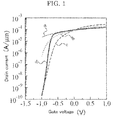
- FIG. 1 is a graph plotting characteristics of transistors in which the gate insulating film is made of materials having an invariable relative dielectric constant and a transistor in which the gate insulating film is made of a dielectric having a variable relative dielectric constant. As plotted in FIG. 1
- a curve c representing the current change rate of a case where the relative dielectric constant is constant at 25 reveal failures to obtain a steep current change rate of lower than 60 mV/decade in the subthreshold region at room temperature
- a curve d representing the current change rate of the case where the dielectric constant changes according to an electric field intensity at the gate electrode reveals a change of the relative dielectric constant characteristic in a manner to intersect the characteristics of the cases where the relative dielectric constant is 5, 10, and 25, i.e., a success in obtaining a steep current change rate of lower than 60 mV/decade in the subthreshold region at room temperature.
- the present invention is based on the finding described above, and solutions to the problems described above are as follows.
- the present invention can solve the various related problems described above and provide a field-effect transistor that is low power-consuming and capable of obtaining a steep current change rate of lower than 60 mV/decade in a subthreshold region at room temperature.
- FIG. 2 is a depictive diagram illustrating a cross-sectional structure of a field-effect transistor according to an embodiment of the present invention.
- a field-effect transistor 10 includes a support substrate 1, an insulating layer 2, a source region 3, a drain region 4, a channel region 5, an interfacial layer 6, a gate insulating film 7, and a gate electrode 8.
- the support substrate 1 is not particularly limited, and an arbitrary support substrate may be selected according to the purpose.
- the support substrate in a known SOI (Silicon on Insulator) substrate may be used.
- the insulating layer 2 is disposed over the support substrate 1.
- the insulating layer 2 is not particularly limited, and an arbitrary insulating layer may be selected according to the purpose.
- the embedded oxide film in the SOI substrate may be used.
- a semiconductor layer 9 in which the source region3, the drain region 4, and the channel region 5 are formed is disposed over the oxide film layer 2.
- the semiconductor layer 9 is not particularly limited, and an arbitrary semiconductor layer may be selected according to the purpose.
- the semiconductor layer in the SOI substrate may be used. That is, it is possible to constitute the support substrate 1, the insulating layer 2, and the semiconductor layer 9 by using the SOI substrate.
- a semiconductor material for forming the semiconductor layer 9 is not particularly limited, and a semiconductor material other than silicon may be selected where appropriate.
- germanium, tin, a mixed crystal of silicon and germanium, a mixed crystal of germanium and tin, and a group III-V compound such as In x Ga 1-x As (where x is greater than or equal to 0.53) and GaSb may be used.
- a thickness of the semiconductor layer 9 is not particularly limited, but is preferably from 6 nm through 10 nm from a viewpoint of obtaining a steep current change rate of lower than 60 mV/decade in the subthreshold region at room temperature.
- the source region 3 and the drain region 4 are formed by ion implantation of an impurity substance into the semiconductor layer 9.
- the impurity substance is not particularly limited so long as the impurity substance is a material that generates carriers.
- Examples of the impurity substance when the source region 3 and the drain region 4 are formed to have an N-type conductivity include P and As.
- Examples of the impurity substance when the source region 3 and the drain region 4 are formed to have a P-type conductivity include B.
- a method for ion implantation is not particularly limited, and may be carried out according to a known ion implantation method.
- the method may be carried out by performing ion implantation into the semiconductor layer 9 with a known ion implantation apparatus using a material gas such as a boron difluoride (BF 2 ) gas, a phosphine (PH 3 ) gas, and an arsine (AsH 3 ) gas or a solid of a material such as solid P and solid As as an ion source.
- a material gas such as a boron difluoride (BF 2 ) gas, a phosphine (PH 3 ) gas, and an arsine (AsH 3 ) gas or a solid of a material such as solid P and solid As as an ion source.
- a concentration of the impurity substance in the source region 3 and the drain region 4 is not particularly limited, but is preferably from 1 ⁇ 10 19 /cm 3 through 1 ⁇ 10 21 /cm 3 in order to suppress a parasitic resistance.
- the channel region 5 is disposed between the source region 3 and the drain region 4 and formed to have the same conductivity type as the source region 3 and the drain region 4 to form an accumulation-operation-type transistor.
- the channel region 5 is not particularly limited, and may be formed according to the same method as the method for forming the source region 3 and the drain region 4.
- the impurity concentration in the channel region 5 is preferably from 4 ⁇ 10 18 /cm 3 through 7 ⁇ 10 18 /cm 3 from a viewpoint of obtaining a steep current change rate of lower than 60 mV/decade in the subthreshold region at room temperature.
- the source region 3, the channel region5, and the drain region 4 that have either an N-type or P-type conductivity in common are formed in the semiconductor layer 9, which enables an accumulation-layer-type transistor operation. That is, when a predetermined gate voltage is set to the gate electrode 8, a field effect generated due to an electric potential difference between the gate electrode 8 and the channel region 5 causes the channel region 5 to be depleted to block a drain current between the source region 3 and the drain region 4 (OFF state).
- the depletion of the channel region 5 shrinks to promote an accumulation layer in which the same carriers as those in the source region 3 and the drain region 4 are accumulated to be formed in the channel region 5, which causes a drain current to flow between the source region 3 and the drain region 4 through the accumulation layer (ON state).
- transistors of the accumulation-operation type are typically normally-on types in which a current flows even when no gate voltage is applied.
- transistors preferable for use in low-power-consuming integrated circuits are normally-off types.
- the field-effect transistor 10 is an accumulation-operation-type transistor of a normally-off type.
- the field-effect transistor 10 operate as a normally-off type, by adjusting a metal material (work function) of the gate electrode 8 and a thickness of the channel region 5 (semiconductor layer 9) according to a known example to thereby set a threshold voltage defining ON-OFF operations to a predetermined value. That is, based on the setting of the threshold voltage, the field-effect transistor 10 switches off when the channel region 5 is depleted to offset an electric field that is generated due to an electric potential difference between the gate electrode 8 and the channel region 5 even when no gate voltage is applied, and switches on when the depletion shrinks upon application of a gate voltage in a positive direction to weaken the electric field.
- the gate insulating film 7 is disposed over the channel region 5 and made of a dielectric having a change gradient of a relative dielectric constant in which the relative dielectric constant changes to decrease according to the magnitude of the gate voltage applied to the gate electrode 8.
- a characteristic of the dielectric will be described with reference to FIG. 3.
- FIG. 3 is a graph plotting electric field intensity-dielectric constant characteristics of dielectrics.
- dielectrics include dielectrics that have a characteristic exemplified by a sign A in FIG. 3 , i.e., a relative dielectric constant that changes in response to changes in electric field intensity (here, such dielectrics will be referred to as nonlinearly responding dielectric), and dielectrics that have a characteristic exemplified by a sign B, i.e., a relative dielectric constant that does not change in response to changes in electric field intensity (here, such dielectrics will be referred to as linearly responding dielectric).
- the linearly responding dielectric include SiO 2 , which is widely used as a gate insulating film of field-effect transistors of the accumulation-operation type and field-effect transistors of an inversion-operation type.
- the field-effect transistor 10 uses the nonlinearly responding dielectric as a material for forming the gate insulating film 7 to utilize the change gradient of the relative dielectric constant in which the relative dielectric constant changes to decrease according to the magnitude of the gate voltage applied to the gate electrode 8 to obtain a steep current change rate of lower than 60 mV/decade in the subthreshold region at room temperature.
- the field-effect transistor 10 using the nonlinearly responding dielectric having the relative dielectric constant that changes according to the magnitude of the gate voltage is operated based on a setting of the gate voltage within a range in which the change gradient of the relative dielectric constant in which the relative dielectric constant changes to decrease is used wholly or partially.
- the relative dielectric constant of the nonlinearly responding dielectric having the characteristic exemplified by the sign A changes according to the electric field intensity.
- the field-effect transistor 10 utilizes the effect of the relative dielectric constant's changing to decrease in response to a change of the electric field intensity at the nonlinearly responding dielectric upon increase of the gate voltage in the operation range of the gate voltage.
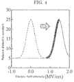
- FIG. 4 is a graph plotting an electric field intensity-dielectric constant characteristic of the nonlinearly responding dielectric.
- a characteristic that the nonlinearly responding dielectric should preferably have is a characteristic represented by a curve that is convex upward and has a local maximum value of the relative dielectric constant in a range of the electric field intensity that does not overlap the origin.
- the nonlinearly responding dielectric may be under an electric field having a high intensity due to a field effect attributed to the aforementioned electric potential difference even in an OFF state in which no gate voltage is applied to the gate electrode 8.
- the nonlinearly responding dielectric having a local maximum value of the relative dielectric constant in a range of the electric field intensity that does not overlap the origin.
- the change gradient of the relative dielectric constant be steep in the field-effect transistor 10 utilizing the change gradient of the relative dielectric constant.
- the nonlinearly responding dielectric have a change gradient of the relative dielectric constant in which when the gate voltage is modulated to a value higher by 0.5 V on an absolute value basis , the relative dielectric constant becomes lower than or equal to a 0.5-times multiple of the relative dielectric constant before modulation.
- the nonlinearly responding dielectric is not particularly limited, and it is preferable that the nonlinearly responding dielectric be constituted by any one of: a superlattice structure formed by laminating layers of a metal oxide having a perovskite-type crystalline structure, a metal oxide having a fluorite-type crystalline structure, and a metal oxide having the perovskite-type crystalline structure of a different kind; a superlattice structure formed by laminating layers of metal oxides having the fluorite-type crystalline structure of different kinds; and a superlattice structure formed by laminating layers of a metal oxide having the perovskite-type crystalline structure and a metal oxide having the fluorite-type crystalline structure, which are examples of dielectrics having the characteristic described above.
- Examples of the metal oxide having the perovskite-type crystalline structure include CaTiO 3 , SrTiO 3 , BaTiO 3 , CaZrO 3 , SrZrO 3 , BaZrO 3 , CaHfO 3 , SrHfO 3 , BaHfO 3 , PbTiO 3 , (Ba, Sr)TiO 3 , Pb(Zr, Ti)O 3 , SrBi 2 Ta 2 O 9 , SrBi 2 Nb 2 O 9 , and Sr 2 Bi 4 Ti 5 O 18 .
- Examples of the metal oxide having the fluorite-type crystalline structure include ZrO 2 , ZrO 2 in which Y is added in an amount of from 9 mol% through 13 mol%, HfO 2 , HfO 2 in which Y is added in an amount of from 9 mol% through 13 mol%, HfO 2 in which La is added in an amount of from 9 mol% through 13 mol%, and (Zr, Hf)O 2 .
- Examples of the superlattice structure include a laminated structure of SrTiO 3 and BaTiO 3 , a laminated structure of SrZrO 3 and BaZrO 3 , a laminated structure of SrHfO 3 and BaHfO 3 , a laminated structure of ZrO 2 and HfO 2 , a laminates structure of SrHfO 3 and HfO 2 , and a laminated structure of SrZrO 3 and ZrO 2 .
- the nonlinearly responding dielectric may be formed according to such known examples.
- a reported example of SrTiO 3 having the perovskite-type crystalline structure (Referential Document 1) and a reported example of the superlattice structure (Referential Document 2) are plotted d in FIG. 5A and FIG. 5B . These graphs both plot electric field dependency of the relative dielectric constant of the nonlinearly responding dielectric.
- a thickness of the gate insulating film 7 made of the nonlinearly responding dielectric is not particularly limited. However, from a viewpoint of obtaining a steep current change rate of lower than 60 mV/decade in the subthreshold region at room temperature, it is preferable that an effective oxide film thickness (EOT; Equivalent Oxide Thickness) of the gate insulating film 7 have a change rate (EOT max /EOT min ) of greater than or equal to 2 when the gate voltage is modulated by 0.5 V. EOT max represents EOT after the gate voltage is modulated, and EOT min represents EOT before the gate voltage is modulated.
- EOT max represents EOT after the gate voltage is modulated
- EOT min represents EOT before the gate voltage is modulated.
- the gate electrode 8 is disposed over the gate insulating film 7.
- a material for forming the gate electrode 8 is not particularly limited, and examples of the material include Al, Au, Pt, W, TaN, TiN, and silicide.
- a method for forming the gate electrode 8 is not particularly limited, and examples of the method include a sputtering method and a CVD (Chemical Vapor Deposition) method.
- a thickness of the gate electrode 8 is not particularly limited and may be from about 10 nm through 50 nm.
- the interfacial layer 6 is disposed between the channel region 5 and the gate insulating film 7.
- the interfacial layer 6 has a function for suppressing interdiffusion of the constituent atoms of the gate insulating film 7 and the channel region 5 between each other, and is disposed as needed depending on the construction of the gate insulating film 7 and the channel region 5.
- a material for forming the interfacial layer 6 is not particularly limited, and examples of the material include HfO 2 , ZrO 2, Al 2 O 3 , SiN, and InP.
- a method for forming the interfacial layer 6 is not particularly limited, and examples of the method include a sputtering method and a CVD method.
- a thickness of the interfacial layer 6 is smaller and preferably smaller than or equal to, for example, 5 nm.
- the EOT of the gate insulating film 7 is set to include an EOT of the interfacial layer 6.
- the gate voltage of the gate electrode 8 is set to 0 or a small value.
- the gate insulating film 7 is under an electric field having a high intensity due to an electric potential difference between the gate electrode 8 and the channel region 5 and in a state of having a high relative dielectric constant according to the characteristic of the nonlinearly responding dielectric plotted in FIG. 4 .
- a strong electric field that balances with the electric field at the gate insulating film 7 is also applied to the channel region 5 in this state, the channel region 5 is depleted to strongly block a drain current between the source region 3 and the drain region 4 (OFF state).
- a gate voltage higher than that in the OFF state is applied to the gate electrode 8.
- the electric field intensity at the gate insulating film 7 weakens to cause a decreasing change of the relative dielectric constant according to the characteristic of the nonlinearly responding dielectric.
- carriers are gradually accumulated in the depleted region in the channel region 5 to form an accumulation layer, which causes a drain current to flow between the source region 3 and the drain region 4 through the accumulation layer in the channel region 5 (ON state).
- the operation range of the gate voltage for ON/OFF switching can be defined by low voltages.
- a configuration of an inversion-operation-type field-effect transistor obtained by forming a gate insulating film with a ferroelectric having a dielectric constant that changes according to an electric field intensity is known to be used for a memory operation purpose.
- a steep current change rate of lower than 60 mV/decade is obtained when a field-effect transistor intended for use as a switching operation purpose is constituted based on the configuration of this inversion-operation-type field-effect transistor. The reason for this is not necessarily certain.
- the reason is inferred to be that in the case of the inversion layer operation, a saddle point at which the drain current becomes constant and the nonlinearly responding dielectric does not function as the gate insulating film is present in the subthreshold region, which inhibits steepening of the current change rate.
- the electric field intensity at the gate insulating film 7 weakens (1.0 MV/cm, see FIG. 4 ), the relative dielectric constant of the gate insulating film 7 decreases (relative dielectric constant: 5, see FIG. 4 ), and a steep rise of the drain current is realized (see the curve d in FIG. 1 ).
- the field-effect transistor of the present invention can also be applied as a so-called P-type transistor that is operated by changing the gate voltage in the negative direction. That is, also in this case, the relative dielectric constant of the gate insulating film 7 and the electric field intensity change in the same way as when the gate voltage is changed in the positive direction. Therefore, a field-effect transistor utilizing this characteristic can be obtained.
- the field-effect transistor 10 having the configuration represented by a SOI-type field-effect transistor obtained by disposing the gate insulating film 7 and the gate electrode 8 in this order over the channel region 5 in the semiconductor layer 9.
- the transistor configuration utilizing the characteristic of the nonlinearly responding dielectric of which the gate insulating film 7 is made is not limited to the SOI type.
- the field-effect transistor of the present invention may be constructed as known transistor configurations such as a bulk type that utilizes a flat surface of a crystalline substrate as a channel, a fin type in which one surface and another surface of a channel region are covered with a gate insulating film and a gate electrode that are formed in a squared-U shape, and a nanowire type in which the circumference of a cylindrical channel region is covered with a gate insulating film and a gate electrode.
- FIG. 6 is a depictive diagram illustrating a cross-sectional structure of the field-effect transistor 20, which is the target of the simulation test.
- the field-effect transistor 20 includes a SOI substrate obtained by laminating, in an order of reciting, an insulating layer 22 and a semiconductor layer 29 in which a source region 23, a drain region 24, and a channel region 25 are formed over a support substrate 21, a gate insulating film 27 disposed over the channel region 25, and a gate electrode 28 disposed over the gate insulating film 27.
- a thickness of a semiconductor layer 29 was 8 nm.
- An impurity introduced into the source region 23 and the drain region 24 by ion implantation was As, and the impurity concentration was 1 ⁇ 10 20 /cm 3 .
- An impurity introduced into the channel region 25 by ion implantation was As, and the impurity concentration was 5 ⁇ 10 18 /cm 3 .
- a relative dielectric constant of the gate insulating film 27 made of the nonlinearly responding dielectric was variable in a range of from 25 through 5.
- a work function of the gate electrode 28 was 5.0 eV.
- FIG. 7 is a graph plotting a gate voltage-drain current characteristic of the field-effect transistor 20.
- the reference sign 31 denotes the gate voltage-drain current characteristic of the field-effect transistor
- the reference sign 32 denotes a drain current rising characteristic in which the current change rate in the subthreshold region at room temperature was 60 mV/decade, which is considered to be the theoretical limit in existing field-effect transistors.
- the reference sign 33 denotes a gate voltage-relative dielectric constant characteristic of the field-effect transistor, and the characteristic has a change gradient in which the relative dielectric constant of the gate insulating film 27 changes to decrease as the gate voltage increases.
- the gate voltage-drain current characteristic of the field-effect transistor 20 exhibits a steeper rise of the drain current than that in the gate voltage-drain current characteristic of the field-effect transistor, with a current change rate in the subthreshold region at room temperature of 48 mV/decade.
- T represents a physical film thickness of the gate insulating film 27
- ⁇ represents the dielectric constant of the gate insulating film
- ⁇ SiO represents a dielectric constant of SiO 2 .
- a relative dielectric constant changing condition effective for obtaining a steep drain current rise was considered based on an EOT change rate (EOT max /EOT min ) of the EOT change plotted in the aforementioned FIG. 8 per 0.5 V modulation of the gate voltage.
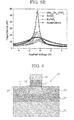
- FIG. 9 plots EOT change rate characteristics when the gate voltage is modulated by 0.5 V.
- the circle marks denote a case where the current change rate was lower than 60 mV/decade
- the cross marks denote a case where the current change rate was higher than or equal to 60 mV/decade.
- EOT max represents EOT after the gate voltage was modulated
- EOT min represents EOT before the gate voltage was modulated.
- FIG. 10 plots a result of calculation of the current change rate (Subthreshold swing) when the thickness of the channel region 25 was varied in the simulation test described above.
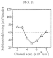
- FIG. 11 plots a result of calculation of the current change rate (Subthreshold swing) when the impurity concentration in the channel region 25 was varied.
- a film formation experiment was conducted in which a film of the nonlinearly responding dielectric having the same characteristic as that of the gate insulating film 27 used in the calculation of the simulation test was actually formed.
- a SrHfO 3 film having a perovskite-type crystalline structure was formed as the film of the nonlinearly responding dielectric.
- sputtering targeting SrO 2 and HfO 2 was performed on a Si substrate set in a vacuum chamber of a RF sputter system (MPS-6000-MLT available from Ulvac, Inc.) under control of the plasma power of the targets and a shutter opening/closing time, to form a SrHfO 3 film having an adjusted chemical composition.
- the Si substrate over which the SrHfO 3 film was formed was subjected to a heating treatment at 1,000°C for 10 seconds under a nitrogen gas atmosphere, to form a SrHfO 3 film having a perovskite-type crystalline structure.
- FIG. 12 plots a result of measurement of the crystalline structure of the SrHfO 3 film by an in-plane X-ray analyzer (a high-resolution X-ray thin film evaluator SUPERLAB available from Rigaku Corporation). As plotted in FIG. 12 , in the present film formation experiment, a single body film of SrHfO 3 having a perovskite-type crystalline structure could be formed over the Si substrate.
- the Si substrate over which the single body film of SrHfO 3 having a perovskite-type crystalline structure was formed was measured for a Sr atom depth distribution with a Rutherford backscattering analyzer (HRBS500 available from Kobe Steel, Ltd.).
- HRBS500 Rutherford backscattering analyzer
- a HfO 2 film having a thickness of 3 nm was once formed as an interfacial layer over a Si substrate, and then a SrHfO 3 film having a perovskite-type crystalline structure was formed over the HfO 2 film in the same manner as described above.
- the HfO 2 film was formed with a RF sputter system (MPS-6000-MLT available from Ulvac, Inc.).
- FIG. 13B The result of measurement of a Sr atom depth distribution when the interfacial layer was formed measured by the Rutherford backscattering analyzer is plotted in FIG. 13B .
- the solid line represents a Sr atom depth distribution after the heating treatment
- the dotted line represents a Sr atom depth distribution before the heating treatment.
Landscapes
- Thin Film Transistor (AREA)
- Insulated Gate Type Field-Effect Transistor (AREA)
- Chemical & Material Sciences (AREA)
- Electrodes Of Semiconductors (AREA)
- Engineering & Computer Science (AREA)
- Materials Engineering (AREA)
- Crystallography & Structural Chemistry (AREA)
- Physics & Mathematics (AREA)
- Optics & Photonics (AREA)
Abstract
Description
- The present invention relates to a field-effect transistor having a steep current change rate in a subthreshold region to suppress a gate voltage required to change a current value by one digit.
- With a view to suppressing power consumption of semiconductor integrated circuits, there is a need for suppressing power consumption of individual transistors, which are the constituting elements.
- As a method for achieving this object, research and development are pursued for suppressing a power required for ON-OFF switching operations of the transistors by providing a steep current change rate in a region (subthreshold region) lower than or equal to a threshold voltage that defines the switching operations. The current change rate in the subthreshold region is an index for a gate voltage (S factor) required for changing a current value by one digit. A lower current change rate enables a steeper switching operation.
- However, in a typical transistor configuration, the current change rate in the subthreshold region at room temperature is higher than or equal to 60 mV/decade theoretically Therefore, there is a problem that a steeper characteristic lower than this cannot be obtained (see, e.g., NPL 1).
- Hence, currently, development of a novel transistor having a steep characteristic represented by the current change rate of lower than 60 mV/decade is sought after based on a configuration different from typical transistors.
- As such a novel transistor, there is proposed, for example, a tunneling field-effect transistor utilizing quantum tunneling (NPL 2).
- However, the proposed tunneling field-effect transistor has a problem of requiring a high gate voltage for its operation in order to apply a high electric field to a tunnel junction to modulate bands and induce tunneling transportation of carriers, thus failing to realize low power consumption.
- Hence, currently, research and development of a novel transistor that is low power-consuming and aims to obtain a steep current change rate of lower than 60 mV/decade in the subthreshold region at room temperature are sought after from various aspects.
-
- NPL 1: Authored by Yuan Taur and Tak H. Ning, Fundamentals of MODERN VLSI DEVICES, Cambridge University Press 1998, p. 128.
- NPL 2: W.Y. Choi, et. al., Electron Device Letters 28 (2007), p. 743.
- The present invention aims to solve the various related problems described above and achieve an object described below. That is, the present invention has an object to provide a field-effect transistor that is low power-consuming and capable of obtaining a steep current change rate of lower than 60 mV/decade in a subthreshold region at room temperature.
- To solve the problems described above, the present inventors have conducted earnest studies and obtained the following finding.
- That is, the present inventors have found that an accumulation-operation-type field-effect transistor can be low power-consuming and obtain a steep current change rate of lower than 60 mV/decade in a subthreshold region at room temperature, if a gate insulating film is made of a dielectric having a change gradient of a relative dielectric constant in which the relative dielectric constant changes to decrease according to the magnitude of a gate voltage applied to a gate electrode.
- This finding will be described with reference to
FIG. 1. FIG. 1 is a graph plotting characteristics of transistors in which the gate insulating film is made of materials having an invariable relative dielectric constant and a transistor in which the gate insulating film is made of a dielectric having a variable relative dielectric constant. As plotted inFIG. 1 , a curve a representing a current change rate (a drain current-gate voltage characteristic) of a case where the relative dielectric constant is constant at 5, a curve b representing the current change rate of a case where the relative dielectric constant is constant at 10, and a curve c representing the current change rate of a case where the relative dielectric constant is constant at 25 reveal failures to obtain a steep current change rate of lower than 60 mV/decade in the subthreshold region at room temperature, whereas a curve d representing the current change rate of the case where the dielectric constant changes according to an electric field intensity at the gate electrode reveals a change of the relative dielectric constant characteristic in a manner to intersect the characteristics of the cases where the relative dielectric constant is 5, 10, and 25, i.e., a success in obtaining a steep current change rate of lower than 60 mV/decade in the subthreshold region at room temperature. - The present invention is based on the finding described above, and solutions to the problems described above are as follows.
- <1> A field-effect transistor of an accumulation-layer-operation type, including:
- a semiconductor layer in which a source region, a channel region, and a drain region that have either an N-type or P-type conductivity in common are formed; and
- a gate electrode disposed adjacent to the channel region via a gate insulating film,
- wherein the gate insulating film is made of a dielectric having a change gradient of a relative dielectric constant in which the relative dielectric constant changes to decrease according to a magnitude of a gate voltage applied to the gate electrode.
- <2> The field-effect transistor according to <1>,
wherein when an origin is set at an electric field intensity of 0 where the electric field intensity is an intensity of an electric field applied to the dielectric, the dielectric has a local maximum value of the relative dielectric constant in a range of the electric field intensity that does not overlap the origin. - <3> The field-effect transistor according to <1> or <2>,
wherein the dielectric has the change gradient of the relative dielectric constant in which when the gate voltage is modulated by 0.5 V, the relative dielectric constant becomes lower than or equal to a 0.5-times multiple of the relative dielectric constant before modulation. - <4> The field-effect transistor according to <1> to <3>,
wherein the dielectric is constituted by any one of: a superlattice structure formed by laminating layers of a metal oxide having a perovskite-type crystalline structure, a metal oxide having a fluorite-type crystalline structure, and a metal oxide having the perovskite-type crystalline structure of a different kind; a superlattice structure formed by laminating layers of metal oxides having the fluorite-type crystalline structure of different kinds; and a superlattice structure formed by laminating layers of a metal oxide having the perovskite-type crystalline structure and a metal oxide having the fluorite-type crystalline structure. - <5> The field-effect transistor according to any one of <1> to <4>,
wherein the semiconductor layer has a thickness of from 6 nm through 10 nm. - <6> The field-effect transistor according to any one of <1> to <5>,
wherein an impurity concentration in the channel region is from 4×10¹⁸/cm3 through 7×1018 cm3. - <7> The field-effect transistor according to any one of <1> to <6>, further including:
- an interfacial layer disposed between the channel region and the gate insulating film.
- <8> The field-effect transistor according to any one of <1> to <7>,
wherein a material of which the semiconductor layer is made is any one of silicon, germanium, tin, a mixed crystal of silicon and germanium, a mixed crystal of germanium and tin, and a group III-V compound. - <9> The field-effect transistor according to any one of <1> to <8>,
wherein the field-effect transistor has a transistor structure of any one of a bulk type, a SOI type, a fin type, and a nanowire type. - The present invention can solve the various related problems described above and provide a field-effect transistor that is low power-consuming and capable of obtaining a steep current change rate of lower than 60 mV/decade in a subthreshold region at room temperature.
-
-
FIG. 1 is a graph plotting characteristics of transistors in which a gate insulating film is made of materials having an invariable relative dielectric constant and a transistor in which a gate insulating film is made of a dielectric having a variable relative dielectric constant. -
FIG. 2 is a depictive diagram illustrating a cross-sectional structure of a field-effect transistor according to an embodiment of the present invention. -
FIG. 3 is a graph plotting electric field intensity-dielectric constant characteristics of dielectrics. -
FIG. 4 is a graph plotting an electric field intensity-dielectric constant characteristic of a nonlinearly responding dielectric. -
FIG. 5A is a graph plotting an example of electric field dependency of a relative dielectric constant of SrTiO3 having a perovskite-type crystalline structure. -
FIG. 5B is a graph plotting an example of electric field (voltage) dependency of a relative dielectric constant (capacitance) of a dielectric having a superlattice structure. -
FIG. 6 is a depictive diagram illustrating a cross-sectional structure of a field-effect transistor, which is a target of a simulation test. -
FIG. 7 is a graph plotting a gate voltage-drain current characteristic of a field-effect transistor. -
FIG. 8 is a graph plotting EOT change of a gate insulating film relative to a gate voltage. -
FIG. 9 is a graph plotting EOT change rate characteristics when a gate voltage is modulated by 0.5 V. -
FIG. 10 is a graph plotting a result of calculation of a current change rate (Subthreshold swing) when a thickness of a channel region is varied. -
FIG. 11 is a graph plotting a result of calculation of a current change rate (Subthreshold swing) when an impurity concentration in a channel region is varied. -
FIG. 12 is a graph plotting a result of measurement of a crystalline structure of a SrHfO3 film. -
FIG. 13A is a graph plotting a result of measurement of a Sr atom depth distribution in a Si substrate over which a single body film of SrHfO3 having a perovskite-type crystalline structure is formed. -
FIG. 13B is a graph plotting a result of measurement of a Sr atom depth distribution when an interfacial layer is formed. - A field-effect transistor of the present invention will be described with reference to mainly
FIG. 2. FIG. 2 is a depictive diagram illustrating a cross-sectional structure of a field-effect transistor according to an embodiment of the present invention. As illustrated inFIG. 2 , a field-effect transistor 10 includes asupport substrate 1, an insulatinglayer 2, asource region 3, adrain region 4, achannel region 5, aninterfacial layer 6, agate insulating film 7, and agate electrode 8. - The
support substrate 1 is not particularly limited, and an arbitrary support substrate may be selected according to the purpose. For example, the support substrate in a known SOI (Silicon on Insulator) substrate may be used. - The insulating
layer 2 is disposed over thesupport substrate 1. The insulatinglayer 2 is not particularly limited, and an arbitrary insulating layer may be selected according to the purpose. For example, the embedded oxide film in the SOI substrate may be used. - A
semiconductor layer 9 in which the source region3, thedrain region 4, and thechannel region 5 are formed is disposed over theoxide film layer 2. Thesemiconductor layer 9 is not particularly limited, and an arbitrary semiconductor layer may be selected according to the purpose. For example, the semiconductor layer in the SOI substrate may be used. That is, it is possible to constitute thesupport substrate 1, the insulatinglayer 2, and thesemiconductor layer 9 by using the SOI substrate. - Although the SOI substrate is raised as an example, a semiconductor material for forming the
semiconductor layer 9 is not particularly limited, and a semiconductor material other than silicon may be selected where appropriate. For example, germanium, tin, a mixed crystal of silicon and germanium, a mixed crystal of germanium and tin, and a group III-V compound such as InxGa1-xAs (where x is greater than or equal to 0.53) and GaSb may be used. - A thickness of the
semiconductor layer 9 is not particularly limited, but is preferably from 6 nm through 10 nm from a viewpoint of obtaining a steep current change rate of lower than 60 mV/decade in the subthreshold region at room temperature. - The
source region 3 and thedrain region 4 are formed by ion implantation of an impurity substance into thesemiconductor layer 9. The impurity substance is not particularly limited so long as the impurity substance is a material that generates carriers. Examples of the impurity substance when thesource region 3 and thedrain region 4 are formed to have an N-type conductivity include P and As. Examples of the impurity substance when thesource region 3 and thedrain region 4 are formed to have a P-type conductivity include B. A method for ion implantation is not particularly limited, and may be carried out according to a known ion implantation method. For example, the method may be carried out by performing ion implantation into thesemiconductor layer 9 with a known ion implantation apparatus using a material gas such as a boron difluoride (BF2) gas, a phosphine (PH3) gas, and an arsine (AsH3) gas or a solid of a material such as solid P and solid As as an ion source. - The
source region 3 and thedrain region 4 formed to have the same conductivity type. A concentration of the impurity substance in thesource region 3 and thedrain region 4 is not particularly limited, but is preferably from 1×10¹⁹ /cm3 through 1×10²¹/cm3 in order to suppress a parasitic resistance. - The
channel region 5 is disposed between thesource region 3 and thedrain region 4 and formed to have the same conductivity type as thesource region 3 and thedrain region 4 to form an accumulation-operation-type transistor. - The
channel region 5 is not particularly limited, and may be formed according to the same method as the method for forming thesource region 3 and thedrain region 4. However, the impurity concentration in thechannel region 5 is preferably from 4×10¹⁸/cm3 through 7×10¹⁸/cm3 from a viewpoint of obtaining a steep current change rate of lower than 60 mV/decade in the subthreshold region at room temperature. - As described above, the
source region 3, the channel region5, and thedrain region 4 that have either an N-type or P-type conductivity in common are formed in thesemiconductor layer 9, which enables an accumulation-layer-type transistor operation. That is, when a predetermined gate voltage is set to thegate electrode 8, a field effect generated due to an electric potential difference between thegate electrode 8 and thechannel region 5 causes thechannel region 5 to be depleted to block a drain current between thesource region 3 and the drain region 4 (OFF state). When a different gate voltage is applied to thegate electrode 8, the depletion of thechannel region 5 shrinks to promote an accumulation layer in which the same carriers as those in thesource region 3 and thedrain region 4 are accumulated to be formed in thechannel region 5, which causes a drain current to flow between thesource region 3 and thedrain region 4 through the accumulation layer (ON state). - Incidentally, transistors of the accumulation-operation type are typically normally-on types in which a current flows even when no gate voltage is applied. However, transistors preferable for use in low-power-consuming integrated circuits are normally-off types. Hence, the field-
effect transistor 10 is an accumulation-operation-type transistor of a normally-off type. - It is possible to make the field-
effect transistor 10 operate as a normally-off type, by adjusting a metal material (work function) of thegate electrode 8 and a thickness of the channel region 5 (semiconductor layer 9) according to a known example to thereby set a threshold voltage defining ON-OFF operations to a predetermined value. That is, based on the setting of the threshold voltage, the field-effect transistor 10 switches off when thechannel region 5 is depleted to offset an electric field that is generated due to an electric potential difference between thegate electrode 8 and thechannel region 5 even when no gate voltage is applied, and switches on when the depletion shrinks upon application of a gate voltage in a positive direction to weaken the electric field. - The
gate insulating film 7 is disposed over thechannel region 5 and made of a dielectric having a change gradient of a relative dielectric constant in which the relative dielectric constant changes to decrease according to the magnitude of the gate voltage applied to thegate electrode 8. A characteristic of the dielectric will be described with reference toFIG. 3. FIG. 3 is a graph plotting electric field intensity-dielectric constant characteristics of dielectrics. - Typically, dielectrics include dielectrics that have a characteristic exemplified by a sign A in
FIG. 3 , i.e., a relative dielectric constant that changes in response to changes in electric field intensity (here, such dielectrics will be referred to as nonlinearly responding dielectric), and dielectrics that have a characteristic exemplified by a sign B, i.e., a relative dielectric constant that does not change in response to changes in electric field intensity (here, such dielectrics will be referred to as linearly responding dielectric). Representative examples of the linearly responding dielectric include SiO2, which is widely used as a gate insulating film of field-effect transistors of the accumulation-operation type and field-effect transistors of an inversion-operation type. In contrast, the field-effect transistor 10 uses the nonlinearly responding dielectric as a material for forming thegate insulating film 7 to utilize the change gradient of the relative dielectric constant in which the relative dielectric constant changes to decrease according to the magnitude of the gate voltage applied to thegate electrode 8 to obtain a steep current change rate of lower than 60 mV/decade in the subthreshold region at room temperature. - The field-
effect transistor 10 using the nonlinearly responding dielectric having the relative dielectric constant that changes according to the magnitude of the gate voltage is operated based on a setting of the gate voltage within a range in which the change gradient of the relative dielectric constant in which the relative dielectric constant changes to decrease is used wholly or partially. - In regard to
FIG. 3 , the relative dielectric constant of the nonlinearly responding dielectric having the characteristic exemplified by the sign A changes according to the electric field intensity. The field-effect transistor 10 utilizes the effect of the relative dielectric constant's changing to decrease in response to a change of the electric field intensity at the nonlinearly responding dielectric upon increase of the gate voltage in the operation range of the gate voltage. - It is preferable that when an origin is set at an applied electric field intensity of 0, the nonlinearly responding dielectric have a local maximum value of the relative dielectric constant in a range of the electric field intensity that does not overlap the origin. This characteristic of the nonlinearly responding dielectric will be described with reference to
FIG. 4. FIG. 4 is a graph plotting an electric field intensity-dielectric constant characteristic of the nonlinearly responding dielectric. - As plotted in
FIG. 4 , a characteristic that the nonlinearly responding dielectric should preferably have is a characteristic represented by a curve that is convex upward and has a local maximum value of the relative dielectric constant in a range of the electric field intensity that does not overlap the origin. - In the accumulation-operation-type field-
effect transistor 10, the nonlinearly responding dielectric may be under an electric field having a high intensity due to a field effect attributed to the aforementioned electric potential difference even in an OFF state in which no gate voltage is applied to thegate electrode 8. Hence, it is preferable to use the nonlinearly responding dielectric having a local maximum value of the relative dielectric constant in a range of the electric field intensity that does not overlap the origin. - From a viewpoint of obtaining a steep current change rate of lower than 60 mV/decade in the subthreshold region at room temperature, it is preferable that the change gradient of the relative dielectric constant be steep in the field-
effect transistor 10 utilizing the change gradient of the relative dielectric constant. Specifically, it is preferable that the nonlinearly responding dielectric have a change gradient of the relative dielectric constant in which when the gate voltage is modulated to a value higher by 0.5 V on an absolute value basis , the relative dielectric constant becomes lower than or equal to a 0.5-times multiple of the relative dielectric constant before modulation. - The nonlinearly responding dielectric is not particularly limited, and it is preferable that the nonlinearly responding dielectric be constituted by any one of: a superlattice structure formed by laminating layers of a metal oxide having a perovskite-type crystalline structure, a metal oxide having a fluorite-type crystalline structure, and a metal oxide having the perovskite-type crystalline structure of a different kind; a superlattice structure formed by laminating layers of metal oxides having the fluorite-type crystalline structure of different kinds; and a superlattice structure formed by laminating layers of a metal oxide having the perovskite-type crystalline structure and a metal oxide having the fluorite-type crystalline structure, which are examples of dielectrics having the characteristic described above.
- Examples of the metal oxide having the perovskite-type crystalline structure include CaTiO3, SrTiO3, BaTiO3, CaZrO3, SrZrO3, BaZrO3, CaHfO3, SrHfO3, BaHfO3, PbTiO3, (Ba, Sr)TiO3, Pb(Zr, Ti)O3, SrBi2Ta2O9, SrBi2Nb2O9, and Sr2Bi4Ti5O18.
- Examples of the metal oxide having the fluorite-type crystalline structure include ZrO2, ZrO2 in which Y is added in an amount of from 9 mol% through 13 mol%, HfO2, HfO2 in which Y is added in an amount of from 9 mol% through 13 mol%, HfO2 in which La is added in an amount of from 9 mol% through 13 mol%, and (Zr, Hf)O2.
- Examples of the superlattice structure include a laminated structure of SrTiO3 and BaTiO3, a laminated structure of SrZrO3 and BaZrO3, a laminated structure of SrHfO3 and BaHfO3, a laminated structure of ZrO2 and HfO2, a laminates structure of SrHfO3 and HfO2, and a laminated structure of SrZrO3 and ZrO2.
- Various reports have been raised as examples of the nonlinearly responding dielectric. The nonlinearly responding dielectric may be formed according to such known examples. As specific examples of the known examples, a reported example of SrTiO3 having the perovskite-type crystalline structure (Referential Document 1) and a reported example of the superlattice structure (Referential Document 2) are plotted d in
FIG. 5A andFIG. 5B . These graphs both plot electric field dependency of the relative dielectric constant of the nonlinearly responding dielectric. - A thickness of the
gate insulating film 7 made of the nonlinearly responding dielectric is not particularly limited. However, from a viewpoint of obtaining a steep current change rate of lower than 60 mV/decade in the subthreshold region at room temperature, it is preferable that an effective oxide film thickness (EOT; Equivalent Oxide Thickness) of thegate insulating film 7 have a change rate (EOTmax/EOTmin) of greater than or equal to 2 when the gate voltage is modulated by 0.5 V. EOTmax represents EOT after the gate voltage is modulated, and EOTmin represents EOT before the gate voltage is modulated. - Referential Document 1: S. Komatsu et al., Jpn. J. Appl. Phys. vol. 37 (1998) p. 5651.
- Referential Document 2: J. Kim et al., Appl. Phys. Lett. vol. 80 (2002) p. 3581.
- The
gate electrode 8 is disposed over thegate insulating film 7. A material for forming thegate electrode 8 is not particularly limited, and examples of the material include Al, Au, Pt, W, TaN, TiN, and silicide. A method for forming thegate electrode 8 is not particularly limited, and examples of the method include a sputtering method and a CVD (Chemical Vapor Deposition) method. A thickness of thegate electrode 8 is not particularly limited and may be from about 10 nm through 50 nm. - The
interfacial layer 6 is disposed between thechannel region 5 and thegate insulating film 7. Theinterfacial layer 6 has a function for suppressing interdiffusion of the constituent atoms of thegate insulating film 7 and thechannel region 5 between each other, and is disposed as needed depending on the construction of thegate insulating film 7 and thechannel region 5. - A material for forming the
interfacial layer 6 is not particularly limited, and examples of the material include HfO2, ZrO2, Al2O3, SiN, and InP. A method for forming theinterfacial layer 6 is not particularly limited, and examples of the method include a sputtering method and a CVD method. - In disposing the
interfacial layer 6, it is more preferable if a thickness of theinterfacial layer 6 is smaller and preferably smaller than or equal to, for example, 5 nm. In disposing theinterfacial layer 6, the EOT of thegate insulating film 7 is set to include an EOT of theinterfacial layer 6. - An operation of the accumulation-operation-type field-
effect transistor 10 having the configuration described above will be described. - First, the gate voltage of the
gate electrode 8 is set to 0 or a small value. At the time, thegate insulating film 7 is under an electric field having a high intensity due to an electric potential difference between thegate electrode 8 and thechannel region 5 and in a state of having a high relative dielectric constant according to the characteristic of the nonlinearly responding dielectric plotted inFIG. 4 . When a strong electric field that balances with the electric field at thegate insulating film 7 is also applied to thechannel region 5 in this state, thechannel region 5 is depleted to strongly block a drain current between thesource region 3 and the drain region 4 (OFF state). - Next, a gate voltage higher than that in the OFF state is applied to the
gate electrode 8. At the time, as the gate voltage increases, the electric field intensity at thegate insulating film 7 weakens to cause a decreasing change of the relative dielectric constant according to the characteristic of the nonlinearly responding dielectric. In response to this decreasing change, carriers are gradually accumulated in the depleted region in thechannel region 5 to form an accumulation layer, which causes a drain current to flow between thesource region 3 and thedrain region 4 through the accumulation layer in the channel region 5 (ON state). - At the time, a steep current change rate during the shift from the OFF state to the ON state of lower than 60 mV/decade can be obtained in the subthreshold region at room temperature.
- Further, the operation range of the gate voltage for ON/OFF switching can be defined by low voltages.
- A configuration of an inversion-operation-type field-effect transistor obtained by forming a gate insulating film with a ferroelectric having a dielectric constant that changes according to an electric field intensity is known to be used for a memory operation purpose. However, there has been no report that a steep current change rate of lower than 60 mV/decade is obtained when a field-effect transistor intended for use as a switching operation purpose is constituted based on the configuration of this inversion-operation-type field-effect transistor. The reason for this is not necessarily certain. However, as a result of a computational study of the present inventors', the reason is inferred to be that in the case of the inversion layer operation, a saddle point at which the drain current becomes constant and the nonlinearly responding dielectric does not function as the gate insulating film is present in the subthreshold region, which inhibits steepening of the current change rate.
- This will be described by taking the characteristics plotted in
FIG. 1 andFIG. 4 for example. When the gate voltage is low (-0.1V, see the curve d inFIG. 1 ), the electric field intensity at thegate insulating film 7 is high (1.5 MV/cm, seeFIG. 4 ) and the relative dielectric constant of thegate insulating film 7 takes a local maximum value (relative dielectric constant: 25, seeFIG. 4 ). - As the gate voltage increases from this state (1.0 V, see the curve d in
FIG. 1 ), the electric field intensity at thegate insulating film 7 weakens (1.0 MV/cm, seeFIG. 4 ), the relative dielectric constant of thegate insulating film 7 decreases (relative dielectric constant: 5, seeFIG. 4 ), and a steep rise of the drain current is realized (see the curve d inFIG. 1 ). - In this example, a case of a so-called N-type transistor where the gate voltage is changed in the positive direction has been described. However, the field-effect transistor of the present invention can also be applied as a so-called P-type transistor that is operated by changing the gate voltage in the negative direction. That is, also in this case, the relative dielectric constant of the
gate insulating film 7 and the electric field intensity change in the same way as when the gate voltage is changed in the positive direction. Therefore, a field-effect transistor utilizing this characteristic can be obtained. - An embodiment of the present invention has been described by raising as an example, the field-
effect transistor 10 having the configuration represented by a SOI-type field-effect transistor obtained by disposing thegate insulating film 7 and thegate electrode 8 in this order over thechannel region 5 in thesemiconductor layer 9. However, the transistor configuration utilizing the characteristic of the nonlinearly responding dielectric of which thegate insulating film 7 is made is not limited to the SOI type. The field-effect transistor of the present invention may be constructed as known transistor configurations such as a bulk type that utilizes a flat surface of a crystalline substrate as a channel, a fin type in which one surface and another surface of a channel region are covered with a gate insulating film and a gate electrode that are formed in a squared-U shape, and a nanowire type in which the circumference of a cylindrical channel region is covered with a gate insulating film and a gate electrode. - A simulation test was conducted for confirming the operation of the field-effect transistor described above. The simulation test was conducted by assuming a field-
effect transistor 20 illustrated inFIG. 6. FIG. 6 is a depictive diagram illustrating a cross-sectional structure of the field-effect transistor 20, which is the target of the simulation test. - The field-
effect transistor 20 includes a SOI substrate obtained by laminating, in an order of reciting, an insulatinglayer 22 and asemiconductor layer 29 in which asource region 23, adrain region 24, and achannel region 25 are formed over asupport substrate 21, agate insulating film 27 disposed over thechannel region 25, and agate electrode 28 disposed over thegate insulating film 27. - Details of the members will be described. A thickness of a
semiconductor layer 29 was 8 nm. An impurity introduced into thesource region 23 and thedrain region 24 by ion implantation was As, and the impurity concentration was 1×10²⁰ /cm3. An impurity introduced into thechannel region 25 by ion implantation was As, and the impurity concentration was 5×10¹⁸ /cm3. A relative dielectric constant of thegate insulating film 27 made of the nonlinearly responding dielectric was variable in a range of from 25 through 5. A work function of thegate electrode 28 was 5.0 eV. - In the simulation test, a drain current when the gate voltage was applied to the
gate electrode 28 of the field-effect transistor 20 while a source electrode was maintained at 0 V and a drain electrode was maintained at 0.1 V was calculated. A simulator used for the calculation was HYENEXX ver. 5.5 developed by Selete, Inc. - The result of the simulation is plotted in
FIG. 7. FIG. 7 is a graph plotting a gate voltage-drain current characteristic of the field-effect transistor 20. InFIG. 7 , thereference sign 31 denotes the gate voltage-drain current characteristic of the field-effect transistor, and thereference sign 32 denotes a drain current rising characteristic in which the current change rate in the subthreshold region at room temperature was 60 mV/decade, which is considered to be the theoretical limit in existing field-effect transistors. Thereference sign 33 denotes a gate voltage-relative dielectric constant characteristic of the field-effect transistor, and the characteristic has a change gradient in which the relative dielectric constant of thegate insulating film 27 changes to decrease as the gate voltage increases. - As plotted in
FIG. 7 , the gate voltage-drain current characteristic of the field-effect transistor 20 exhibits a steeper rise of the drain current than that in the gate voltage-drain current characteristic of the field-effect transistor, with a current change rate in the subthreshold region at room temperature of 48 mV/decade. - The change of the relative dielectric constant of the
gate insulating film 27 relative to the gate voltage, which was used for the calculation of the simulation test, will be described. As indicted by a formula (1) below, there is a relationship that the EOT of thegate insulating film 27 made of the nonlinearly responding dielectric is the minimum when the relative dielectric constant is the maximum, whereas the EOT is the maximum when the relative dielectric constant is the minimum. The change of the EOT of thegate insulating film 27 relative to the gate voltage is plotted inFig. 8 . In the simulation test, the calculation was performed using this EOT change characteristic.
- In the formula (1) above, T represents a physical film thickness of the
gate insulating film 27, ε represents the dielectric constant of the gate insulating film, and ε SiO, represents a dielectric constant of SiO2. - As described above, a drain current rising characteristic that was steeper than the current change rate in the subthreshold region at room temperature of 60 mV/decade, which is the theoretical limit in existing field-effect transistors, was obtained in the simulation test.
- Further, the result of a consideration about conditions for obtaining a steep drain current rising characteristic will be described below.
- First, a case where the EOT changing characteristic was varied will be described. From a viewpoint of obtaining a steep drain current rise, it is necessary that the relative dielectric constant largely change when the gate voltage is modulated by 0.5 V.
- Here, a relative dielectric constant changing condition effective for obtaining a steep drain current rise was considered based on an EOT change rate (EOTmax/EOTmin) of the EOT change plotted in the aforementioned
FIG. 8 per 0.5 V modulation of the gate voltage. -
FIG. 9 plots EOT change rate characteristics when the gate voltage is modulated by 0.5 V. InFIG. 8 , the circle marks denote a case where the current change rate was lower than 60 mV/decade, and the cross marks denote a case where the current change rate was higher than or equal to 60 mV/decade. EOTmax represents EOT after the gate voltage was modulated, and EOTmin represents EOT before the gate voltage was modulated. - As plotted in
FIG. 9 , steep current rising characteristics in which the current change rate was lower than 60 mV/decade were obtained when the EOT change rate (EOTmax/EOTmin) per 0.5 V modulation of the gate voltage was greater than or equal to 2. This means that thegate insulating film 27 had a change gradient of the relative dielectric constant in which when the gate voltage was modulated by 0.5 V, the relative dielectric constant became lower than or equal to a 0.5-times multiple of the relative dielectric constant before the gate voltage was modulated. - Next, a relationship between the thickness of the
channel region 25 in thesemiconductor layer 29 and the current change rate will be described. -
FIG. 10 plots a result of calculation of the current change rate (Subthreshold swing) when the thickness of thechannel region 25 was varied in the simulation test described above. - As plotted in
FIG. 10 , it is seen that a steep current rising characteristic in which the current change rate was lower than 60 mV/decade was obtained when the thickness of thechannel region 25 was from 6 nm through 10 nm. - Next, a relationship between the impurity concentration in the
channel region 25 in thesemiconductor layer 29 and the current change rate will be described. -
FIG. 11 plots a result of calculation of the current change rate (Subthreshold swing) when the impurity concentration in thechannel region 25 was varied. - As plotted in
FIG. 11 , it is seen that a steep current rising characteristic in which the current change rate was lower than 60 mV/decade was obtained when the impurity concentration in thechannel region 25 was from 4×10¹⁸ /cm3 through 7×10¹⁸/cm3. - A film formation experiment was conducted in which a film of the nonlinearly responding dielectric having the same characteristic as that of the
gate insulating film 27 used in the calculation of the simulation test was actually formed. Here, a SrHfO3 film having a perovskite-type crystalline structure was formed as the film of the nonlinearly responding dielectric. - First, under an Ar gas atmosphere, sputtering targeting SrO2 and HfO2 was performed on a Si substrate set in a vacuum chamber of a RF sputter system (MPS-6000-MLT available from Ulvac, Inc.) under control of the plasma power of the targets and a shutter opening/closing time, to form a SrHfO3 film having an adjusted chemical composition. Next, the Si substrate over which the SrHfO3 film was formed was subjected to a heating treatment at 1,000°C for 10 seconds under a nitrogen gas atmosphere, to form a SrHfO3 film having a perovskite-type crystalline structure.
-
FIG. 12 plots a result of measurement of the crystalline structure of the SrHfO3 film by an in-plane X-ray analyzer (a high-resolution X-ray thin film evaluator SUPERLAB available from Rigaku Corporation). As plotted inFIG. 12 , in the present film formation experiment, a single body film of SrHfO3 having a perovskite-type crystalline structure could be formed over the Si substrate. - Here, the Si substrate over which the single body film of SrHfO3 having a perovskite-type crystalline structure was formed was measured for a Sr atom depth distribution with a Rutherford backscattering analyzer (HRBS500 available from Kobe Steel, Ltd.). The result of the measurement is plotted in
FIG. 13A . InFIG. 13A , the solid line represents a Sr atom depth distribution after the heating treatment, and the dotted line represents a Sr atom depth distribution before the heating treatment. - As plotted in
FIG. 13A , the position and width of the energy at and over which a signal intensity appeared before the heating treatment were different from those after the heating treatment. This suggests that some of the Sr atoms reacted with the Si substrate and diffused, to generate a dispersion in the depth distribution. - In view of this fact, a HfO2 film having a thickness of 3 nm was once formed as an interfacial layer over a Si substrate, and then a SrHfO3 film having a perovskite-type crystalline structure was formed over the HfO2 film in the same manner as described above. Here, the HfO2 film was formed with a RF sputter system (MPS-6000-MLT available from Ulvac, Inc.).
- The result of measurement of a Sr atom depth distribution when the interfacial layer was formed measured by the Rutherford backscattering analyzer is plotted in
FIG. 13B . InFIG. 13B , the solid line represents a Sr atom depth distribution after the heating treatment, and the dotted line represents a Sr atom depth distribution before the heating treatment. - As plotted in
FIG. 13B , when the interfacial layer was formed, the position and width of the energy at and over which a signal intensity appeared before the heating treatment were substantially the same as those after the heating treatment. - Hence, when the interfacial layer was formed, it was possible to suppress diffusion of the Sr atoms into the Si substrate.
-
- 1, 21 support substrate
- 2, 22 insulating layer
- 3, 23 source region
- 4, 24 drain region
- 5, 25 channel region
- 6 interfacial layer
- 7, 27 gate insulating film
- 8, 28 gate electrode
- 9, 29 semiconductor layer
- 10, 20 field-effect transistor
- 31, 32 gate voltage-drain current characteristic of field-effect transistor
- 33 gate voltage-relative dielectric constant characteristic of field-effect transistor
Claims (9)
- A field-effect transistor of an accumulation-layer-operation type, comprising:a semiconductor layer in which a source region, a channel region, and a drain region that have either an N-type or P-type conductivity in common are formed; anda gate electrode disposed adjacent to the channel region via a gate insulating film,wherein the gate insulating film is made of a dielectric having a change gradient of a relative dielectric constant in which the relative dielectric constant changes to decrease according to a magnitude of a gate voltage applied to the gate electrode.
- The field-effect transistor according to claim 1,
wherein when an origin is set at an electric field intensity of 0 where the electric field intensity is an intensity of an electric field applied to the dielectric, the dielectric has a local maximum value of the relative dielectric constant in a range of the electric field intensity that does not overlap the origin. - The field-effect transistor according to claim 1 or 2,
wherein the dielectric has the change gradient of the relative dielectric constant in which when the gate voltage is modulated by 0.5 V, the relative dielectric constant becomes lower than or equal to a 0.5-times multiple of the relative dielectric constant before modulation. - The field-effect transistor according to claims 1 to 3,
wherein the dielectric is constituted by any one of: a superlattice structure formed by laminating layers of a metal oxide having a perovskite-type crystalline structure, a metal oxide having a fluorite-type crystalline structure, and a metal oxide having the perovskite-type crystalline structure of a different kind; a superlattice structure formed by laminating layers of metal oxides having the fluorite-type crystalline structure of different kinds; and a superlattice structure formed by laminating layers of a metal oxide having the perovskite-type crystalline structure and a metal oxide having the fluorite-type crystalline structure. - The field-effect transistor according to any one of claims 1 to 4,
wherein the semiconductor layer has a thickness of from 6 nm through 10 nm. - The field-effect transistor according to any one of claims 1 to 5,
wherein an impurity concentration in the channel region is from 4×10¹⁸/cm3 through 7×1018 cm3. - The field-effect transistor according to any one of claims 1 to 6, further comprising:an interfacial layer disposed between the channel region and the gate insulating film.
- The field-effect transistor according to any one of claims 1 to 7,
wherein a material of which the semiconductor layer is made is any one of silicon, germanium, tin, a mixed crystal of silicon and germanium, a mixed crystal of germanium and tin, and a group III-V compound. - The field-effect transistor according to any one of claims 1 to 8,
wherein the field-effect transistor has a transistor structure of any one of a bulk type, a SOI type, a fin type, and a nanowire-type.
Applications Claiming Priority (2)
| Application Number | Priority Date | Filing Date | Title |
|---|---|---|---|
| JP2013218870 | 2013-10-22 | ||
| PCT/JP2014/071254 WO2015059986A1 (en) | 2013-10-22 | 2014-08-12 | Field-effect transistor |
Publications (3)
| Publication Number | Publication Date |
|---|---|
| EP3062351A1 true EP3062351A1 (en) | 2016-08-31 |
| EP3062351A4 EP3062351A4 (en) | 2017-05-10 |
| EP3062351B1 EP3062351B1 (en) | 2020-11-04 |
Family
ID=52992595
Family Applications (1)
| Application Number | Title | Priority Date | Filing Date |
|---|---|---|---|
| EP14854905.8A Not-in-force EP3062351B1 (en) | 2013-10-22 | 2014-08-12 | Field-effect transistor |
Country Status (5)
| Country | Link |
|---|---|
| US (1) | US9698235B2 (en) |
| EP (1) | EP3062351B1 (en) |
| JP (1) | JP6041281B2 (en) |
| TW (1) | TWI597844B (en) |
| WO (1) | WO2015059986A1 (en) |
Families Citing this family (8)
| Publication number | Priority date | Publication date | Assignee | Title |
|---|---|---|---|---|
| US10276663B2 (en) | 2016-07-18 | 2019-04-30 | United Microelectronics Corp. | Tunneling transistor and method of fabricating the same |
| JP7016177B2 (en) * | 2017-09-29 | 2022-02-04 | 国立研究開発法人産業技術総合研究所 | Semiconductor device |
| US11444171B2 (en) * | 2019-03-06 | 2022-09-13 | Intel Corporation | Self-aligned gate endcap (SAGE) architecture having gate or contact plugs |
| US11063131B2 (en) * | 2019-06-13 | 2021-07-13 | Intel Corporation | Ferroelectric or anti-ferroelectric trench capacitor with spacers for sidewall strain engineering |
| WO2022052045A1 (en) * | 2020-09-11 | 2022-03-17 | 北京大学深圳研究生院 | Negative-capacitance junction-less nanowire field effect transistor and manufacturing method therefor |
| US11581334B2 (en) * | 2021-02-05 | 2023-02-14 | Taiwan Semiconductor Manufacturing Company, Ltd. | Cocktail layer over gate dielectric layer of FET FeRAM |
| KR20230006964A (en) | 2021-07-05 | 2023-01-12 | 삼성전자주식회사 | Semiconductor device |
| CN118335797B (en) * | 2024-04-03 | 2025-08-19 | 苏州华太电子技术股份有限公司 | Semiconductor structure and semiconductor device |
Family Cites Families (6)
| Publication number | Priority date | Publication date | Assignee | Title |
|---|---|---|---|---|
| US5198994A (en) * | 1988-08-31 | 1993-03-30 | Kabushiki Kaisha Toshiba | Ferroelectric memory device |
| US6242771B1 (en) | 1998-01-02 | 2001-06-05 | Sharp Laboratories Of America, Inc. | Chemical vapor deposition of PB5GE3O11 thin film for ferroelectric applications |
| US6246076B1 (en) * | 1998-08-28 | 2001-06-12 | Cree, Inc. | Layered dielectric on silicon carbide semiconductor structures |
| WO2004008544A1 (en) * | 2002-07-16 | 2004-01-22 | Nec Corporation | Semiconductor device, production method and production device thereof |
| GB0427900D0 (en) | 2004-12-21 | 2005-01-19 | Koninkl Philips Electronics Nv | Semiconductor device with high dielectric constant gate insulator and method of manufacture |
| JP5329024B2 (en) * | 2006-06-27 | 2013-10-30 | 国立大学法人東北大学 | Semiconductor device |
-
2014
- 2014-08-12 US US15/031,110 patent/US9698235B2/en not_active Expired - Fee Related
- 2014-08-12 EP EP14854905.8A patent/EP3062351B1/en not_active Not-in-force
- 2014-08-12 WO PCT/JP2014/071254 patent/WO2015059986A1/en not_active Ceased
- 2014-08-12 JP JP2015543739A patent/JP6041281B2/en not_active Expired - Fee Related
- 2014-08-21 TW TW103128861A patent/TWI597844B/en not_active IP Right Cessation
Also Published As
| Publication number | Publication date |
|---|---|
| EP3062351B1 (en) | 2020-11-04 |
| WO2015059986A1 (en) | 2015-04-30 |
| JP6041281B2 (en) | 2016-12-07 |
| TWI597844B (en) | 2017-09-01 |
| US9698235B2 (en) | 2017-07-04 |
| US20160308019A1 (en) | 2016-10-20 |
| JPWO2015059986A1 (en) | 2017-03-09 |
| EP3062351A4 (en) | 2017-05-10 |
| TW201517273A (en) | 2015-05-01 |
Similar Documents
| Publication | Publication Date | Title |
|---|---|---|
| EP3062351B1 (en) | Field-effect transistor | |
| US20230268439A1 (en) | Electronic device including ferroelectric layer | |
| JP7471787B2 (en) | Electronic device and method for manufacturing same | |
| Afouxenidis et al. | ZnO-based thin film transistors employing aluminum titanate gate dielectrics deposited by spray pyrolysis at ambient air | |
| US11522082B2 (en) | Electronic device and method of manufacturing the same | |
| US20200035807A1 (en) | Semiconductor device and forming method thereof | |
| KR101552975B1 (en) | Oxide semiconductor and thin film transistor including the same | |
| US20210280720A1 (en) | Ferroelectric thin-film structure and electronic device including the same | |
| KR20140056210A (en) | Semiconductor device | |
| KR20210119199A (en) | Electronic device and method of manufacturing the same | |
| US11929402B2 (en) | Field-effect transistor and method for designing same | |
| Kim et al. | Effect of Al concentration on Al-doped ZnO channels fabricated by atomic-layer deposition for top-gate oxide thin-film transistor applications | |
| Kim et al. | Synergic Impacts of CF4 Plasma Treatment and Post-thermal Annealing on the Nonvolatile Memory Performance of Charge-Trap-Assisted Memory Thin-Film Transistors Using Al–HfO2 Charge Trap and In–Ga–Zn–O Active Channel Layers | |
| Fukushima et al. | Electrical characteristics of controlled-polarization-type ferroelectric-gate field-effect transistor | |
| KR20210117005A (en) | Semiconductor device and capacitor including hydrogen-incorporated oxide layer | |
| Ohmi et al. | Influence of XeCl excimer laser annealing on the ferroelectric nondoped HfO2 formation deposited on a Si (100) substrate | |
| Ruzgar et al. | Electrical performance of ZnO thin film transistors having different active layer thickness | |
| Tran et al. | Boron-Doped Aluminum Nitride Ferroelectric Field-Effect Transistors with ZnO Semiconductor Channel | |
| Kim et al. | Effects of Li doping on the negative bias stress stability of solution-processed ZnO thin film transistors | |
| Fujimura et al. | Novel Ferroelectric Gate Field-Effect Transistors (FeFETs); Controlled Polarization-Type FeFETs | |
| Prasar et al. | First Principles Study of Electric-Field-Driven Surface Polarization in Graphene/SrTiO₃ Heterostructures | |
| Lim et al. | Characteristics of a‐IZO TFTs with high‐κ HfSiOx gate insulator annealed in various conditions | |
| Samb et al. | Thinning the active layer of TFTs | |
| Shan et al. | TiOx-based thin-film transistors prepared by femtosecond laser pre-annealing | |
| Fujimura et al. | Novel Ferroelectric-Gate Field-Effect Thin Film Transistors (FeTFTs): Controlled Polarization-Type FeTFTs |
Legal Events
| Date | Code | Title | Description |
|---|---|---|---|
| PUAI | Public reference made under article 153(3) epc to a published international application that has entered the european phase |
Free format text: ORIGINAL CODE: 0009012 |
|
| 17P | Request for examination filed |
Effective date: 20160407 |
|
| AK | Designated contracting states |
Kind code of ref document: A1 Designated state(s): AL AT BE BG CH CY CZ DE DK EE ES FI FR GB GR HR HU IE IS IT LI LT LU LV MC MK MT NL NO PL PT RO RS SE SI SK SM TR |
|
| AX | Request for extension of the european patent |
Extension state: BA ME |
|
| RIC1 | Information provided on ipc code assigned before grant |
Ipc: H01L 29/786 20060101AFI20161011BHEP Ipc: H01L 21/336 20060101ALI20161011BHEP Ipc: H01L 21/316 20060101ALI20161011BHEP Ipc: H01L 29/78 20060101ALI20161011BHEP |
|
| RIN1 | Information on inventor provided before grant (corrected) |
Inventor name: OTA HIROYUKI Inventor name: MIGITA SHINJI Inventor name: FUKUDA KOICHI |
|
| DAX | Request for extension of the european patent (deleted) | ||
| A4 | Supplementary search report drawn up and despatched |
Effective date: 20170410 |
|
| RIC1 | Information provided on ipc code assigned before grant |
Ipc: H01L 29/51 20060101ALI20170404BHEP Ipc: H01L 21/316 20060101ALI20170404BHEP Ipc: H01L 29/786 20060101AFI20170404BHEP Ipc: H01L 21/336 20060101ALI20170404BHEP Ipc: H01L 29/78 20060101ALI20170404BHEP |
|
| STAA | Information on the status of an ep patent application or granted ep patent |
Free format text: STATUS: EXAMINATION IS IN PROGRESS |
|
| 17Q | First examination report despatched |
Effective date: 20190624 |
|
| GRAP | Despatch of communication of intention to grant a patent |
Free format text: ORIGINAL CODE: EPIDOSNIGR1 |
|
| STAA | Information on the status of an ep patent application or granted ep patent |
Free format text: STATUS: GRANT OF PATENT IS INTENDED |
|
| INTG | Intention to grant announced |
Effective date: 20200526 |
|
| GRAS | Grant fee paid |
Free format text: ORIGINAL CODE: EPIDOSNIGR3 |
|
| GRAA | (expected) grant |
Free format text: ORIGINAL CODE: 0009210 |
|
| STAA | Information on the status of an ep patent application or granted ep patent |
Free format text: STATUS: THE PATENT HAS BEEN GRANTED |
|
| REG | Reference to a national code |
Ref country code: DE Ref legal event code: R083 Ref document number: 602014072114 Country of ref document: DE |
|
| AK | Designated contracting states |
Kind code of ref document: B1 Designated state(s): AL AT BE BG CH CY CZ DE DK EE ES FI FR GB GR HR HU IE IS IT LI LT LU LV MC MK MT NL NO PL PT RO RS SE SI SK SM TR |
|
| REG | Reference to a national code |
Ref country code: GB Ref legal event code: FG4D |
|
| RIN2 | Information on inventor provided after grant (corrected) |
Inventor name: OTA, HIROYUKI Inventor name: FUKUDA ,KOICHI Inventor name: MIGITA, SHINJI |
|
| REG | Reference to a national code |
Ref country code: CH Ref legal event code: EP |
|
| REG | Reference to a national code |
Ref country code: AT Ref legal event code: REF Ref document number: 1331942 Country of ref document: AT Kind code of ref document: T Effective date: 20201115 |
|
| REG | Reference to a national code |
Ref country code: IE Ref legal event code: FG4D |
|
| REG | Reference to a national code |
Ref country code: DE Ref legal event code: R096 Ref document number: 602014072114 Country of ref document: DE |
|
| REG | Reference to a national code |
Ref country code: NL Ref legal event code: MP Effective date: 20201104 |
|
| REG | Reference to a national code |
Ref country code: AT Ref legal event code: MK05 Ref document number: 1331942 Country of ref document: AT Kind code of ref document: T Effective date: 20201104 |
|
| PG25 | Lapsed in a contracting state [announced via postgrant information from national office to epo] |
Ref country code: NO Free format text: LAPSE BECAUSE OF FAILURE TO SUBMIT A TRANSLATION OF THE DESCRIPTION OR TO PAY THE FEE WITHIN THE PRESCRIBED TIME-LIMIT Effective date: 20210204 Ref country code: PT Free format text: LAPSE BECAUSE OF FAILURE TO SUBMIT A TRANSLATION OF THE DESCRIPTION OR TO PAY THE FEE WITHIN THE PRESCRIBED TIME-LIMIT Effective date: 20210304 Ref country code: RS Free format text: LAPSE BECAUSE OF FAILURE TO SUBMIT A TRANSLATION OF THE DESCRIPTION OR TO PAY THE FEE WITHIN THE PRESCRIBED TIME-LIMIT Effective date: 20201104 Ref country code: FI Free format text: LAPSE BECAUSE OF FAILURE TO SUBMIT A TRANSLATION OF THE DESCRIPTION OR TO PAY THE FEE WITHIN THE PRESCRIBED TIME-LIMIT Effective date: 20201104 Ref country code: GR Free format text: LAPSE BECAUSE OF FAILURE TO SUBMIT A TRANSLATION OF THE DESCRIPTION OR TO PAY THE FEE WITHIN THE PRESCRIBED TIME-LIMIT Effective date: 20210205 |
|
| PG25 | Lapsed in a contracting state [announced via postgrant information from national office to epo] |
Ref country code: SE Free format text: LAPSE BECAUSE OF FAILURE TO SUBMIT A TRANSLATION OF THE DESCRIPTION OR TO PAY THE FEE WITHIN THE PRESCRIBED TIME-LIMIT Effective date: 20201104 Ref country code: IS Free format text: LAPSE BECAUSE OF FAILURE TO SUBMIT A TRANSLATION OF THE DESCRIPTION OR TO PAY THE FEE WITHIN THE PRESCRIBED TIME-LIMIT Effective date: 20210304 Ref country code: PL Free format text: LAPSE BECAUSE OF FAILURE TO SUBMIT A TRANSLATION OF THE DESCRIPTION OR TO PAY THE FEE WITHIN THE PRESCRIBED TIME-LIMIT Effective date: 20201104 Ref country code: LV Free format text: LAPSE BECAUSE OF FAILURE TO SUBMIT A TRANSLATION OF THE DESCRIPTION OR TO PAY THE FEE WITHIN THE PRESCRIBED TIME-LIMIT Effective date: 20201104 Ref country code: AT Free format text: LAPSE BECAUSE OF FAILURE TO SUBMIT A TRANSLATION OF THE DESCRIPTION OR TO PAY THE FEE WITHIN THE PRESCRIBED TIME-LIMIT Effective date: 20201104 Ref country code: ES Free format text: LAPSE BECAUSE OF FAILURE TO SUBMIT A TRANSLATION OF THE DESCRIPTION OR TO PAY THE FEE WITHIN THE PRESCRIBED TIME-LIMIT Effective date: 20201104 Ref country code: BG Free format text: LAPSE BECAUSE OF FAILURE TO SUBMIT A TRANSLATION OF THE DESCRIPTION OR TO PAY THE FEE WITHIN THE PRESCRIBED TIME-LIMIT Effective date: 20210204 |
|
| REG | Reference to a national code |
Ref country code: LT Ref legal event code: MG9D |
|
| PG25 | Lapsed in a contracting state [announced via postgrant information from national office to epo] |
Ref country code: HR Free format text: LAPSE BECAUSE OF FAILURE TO SUBMIT A TRANSLATION OF THE DESCRIPTION OR TO PAY THE FEE WITHIN THE PRESCRIBED TIME-LIMIT Effective date: 20201104 |
|
| PG25 | Lapsed in a contracting state [announced via postgrant information from national office to epo] |
Ref country code: SK Free format text: LAPSE BECAUSE OF FAILURE TO SUBMIT A TRANSLATION OF THE DESCRIPTION OR TO PAY THE FEE WITHIN THE PRESCRIBED TIME-LIMIT Effective date: 20201104 Ref country code: RO Free format text: LAPSE BECAUSE OF FAILURE TO SUBMIT A TRANSLATION OF THE DESCRIPTION OR TO PAY THE FEE WITHIN THE PRESCRIBED TIME-LIMIT Effective date: 20201104 Ref country code: LT Free format text: LAPSE BECAUSE OF FAILURE TO SUBMIT A TRANSLATION OF THE DESCRIPTION OR TO PAY THE FEE WITHIN THE PRESCRIBED TIME-LIMIT Effective date: 20201104 Ref country code: SM Free format text: LAPSE BECAUSE OF FAILURE TO SUBMIT A TRANSLATION OF THE DESCRIPTION OR TO PAY THE FEE WITHIN THE PRESCRIBED TIME-LIMIT Effective date: 20201104 Ref country code: EE Free format text: LAPSE BECAUSE OF FAILURE TO SUBMIT A TRANSLATION OF THE DESCRIPTION OR TO PAY THE FEE WITHIN THE PRESCRIBED TIME-LIMIT Effective date: 20201104 Ref country code: CZ Free format text: LAPSE BECAUSE OF FAILURE TO SUBMIT A TRANSLATION OF THE DESCRIPTION OR TO PAY THE FEE WITHIN THE PRESCRIBED TIME-LIMIT Effective date: 20201104 |
|
| REG | Reference to a national code |
Ref country code: DE Ref legal event code: R097 Ref document number: 602014072114 Country of ref document: DE |
|
| PG25 | Lapsed in a contracting state [announced via postgrant information from national office to epo] |
Ref country code: DK Free format text: LAPSE BECAUSE OF FAILURE TO SUBMIT A TRANSLATION OF THE DESCRIPTION OR TO PAY THE FEE WITHIN THE PRESCRIBED TIME-LIMIT Effective date: 20201104 |
|
| PLBE | No opposition filed within time limit |
Free format text: ORIGINAL CODE: 0009261 |
|
| STAA | Information on the status of an ep patent application or granted ep patent |
Free format text: STATUS: NO OPPOSITION FILED WITHIN TIME LIMIT |
|
| 26N | No opposition filed |
Effective date: 20210805 |
|
| PG25 | Lapsed in a contracting state [announced via postgrant information from national office to epo] |
Ref country code: IT Free format text: LAPSE BECAUSE OF FAILURE TO SUBMIT A TRANSLATION OF THE DESCRIPTION OR TO PAY THE FEE WITHIN THE PRESCRIBED TIME-LIMIT Effective date: 20201104 Ref country code: AL Free format text: LAPSE BECAUSE OF FAILURE TO SUBMIT A TRANSLATION OF THE DESCRIPTION OR TO PAY THE FEE WITHIN THE PRESCRIBED TIME-LIMIT Effective date: 20201104 Ref country code: NL Free format text: LAPSE BECAUSE OF FAILURE TO SUBMIT A TRANSLATION OF THE DESCRIPTION OR TO PAY THE FEE WITHIN THE PRESCRIBED TIME-LIMIT Effective date: 20201104 |
|
| PG25 | Lapsed in a contracting state [announced via postgrant information from national office to epo] |
Ref country code: SI Free format text: LAPSE BECAUSE OF FAILURE TO SUBMIT A TRANSLATION OF THE DESCRIPTION OR TO PAY THE FEE WITHIN THE PRESCRIBED TIME-LIMIT Effective date: 20201104 |
|
| REG | Reference to a national code |
Ref country code: CH Ref legal event code: PL |
|
| PG25 | Lapsed in a contracting state [announced via postgrant information from national office to epo] |
Ref country code: MC Free format text: LAPSE BECAUSE OF FAILURE TO SUBMIT A TRANSLATION OF THE DESCRIPTION OR TO PAY THE FEE WITHIN THE PRESCRIBED TIME-LIMIT Effective date: 20201104 |
|
| REG | Reference to a national code |
Ref country code: BE Ref legal event code: MM Effective date: 20210831 |
|
| GBPC | Gb: european patent ceased through non-payment of renewal fee |
Effective date: 20210812 |
|
| PG25 | Lapsed in a contracting state [announced via postgrant information from national office to epo] |
Ref country code: LI Free format text: LAPSE BECAUSE OF NON-PAYMENT OF DUE FEES Effective date: 20210831 Ref country code: CH Free format text: LAPSE BECAUSE OF NON-PAYMENT OF DUE FEES Effective date: 20210831 |
|
| PG25 | Lapsed in a contracting state [announced via postgrant information from national office to epo] |
Ref country code: IS Free format text: LAPSE BECAUSE OF FAILURE TO SUBMIT A TRANSLATION OF THE DESCRIPTION OR TO PAY THE FEE WITHIN THE PRESCRIBED TIME-LIMIT Effective date: 20210304 Ref country code: LU Free format text: LAPSE BECAUSE OF NON-PAYMENT OF DUE FEES Effective date: 20210812 |
|
| PG25 | Lapsed in a contracting state [announced via postgrant information from national office to epo] |
Ref country code: IE Free format text: LAPSE BECAUSE OF NON-PAYMENT OF DUE FEES Effective date: 20210812 Ref country code: GB Free format text: LAPSE BECAUSE OF NON-PAYMENT OF DUE FEES Effective date: 20210812 Ref country code: FR Free format text: LAPSE BECAUSE OF NON-PAYMENT OF DUE FEES Effective date: 20210831 Ref country code: BE Free format text: LAPSE BECAUSE OF NON-PAYMENT OF DUE FEES Effective date: 20210831 |
|
| PGFP | Annual fee paid to national office [announced via postgrant information from national office to epo] |
Ref country code: DE Payment date: 20220620 Year of fee payment: 9 |
|
| PG25 | Lapsed in a contracting state [announced via postgrant information from national office to epo] |
Ref country code: HU Free format text: LAPSE BECAUSE OF FAILURE TO SUBMIT A TRANSLATION OF THE DESCRIPTION OR TO PAY THE FEE WITHIN THE PRESCRIBED TIME-LIMIT; INVALID AB INITIO Effective date: 20140812 |
|
| PG25 | Lapsed in a contracting state [announced via postgrant information from national office to epo] |
Ref country code: CY Free format text: LAPSE BECAUSE OF FAILURE TO SUBMIT A TRANSLATION OF THE DESCRIPTION OR TO PAY THE FEE WITHIN THE PRESCRIBED TIME-LIMIT Effective date: 20201104 |
|
| REG | Reference to a national code |
Ref country code: DE Ref legal event code: R119 Ref document number: 602014072114 Country of ref document: DE |
|
| PG25 | Lapsed in a contracting state [announced via postgrant information from national office to epo] |
Ref country code: MK Free format text: LAPSE BECAUSE OF FAILURE TO SUBMIT A TRANSLATION OF THE DESCRIPTION OR TO PAY THE FEE WITHIN THE PRESCRIBED TIME-LIMIT Effective date: 20201104 |
|
| PG25 | Lapsed in a contracting state [announced via postgrant information from national office to epo] |
Ref country code: DE Free format text: LAPSE BECAUSE OF NON-PAYMENT OF DUE FEES Effective date: 20240301 |
|
| PG25 | Lapsed in a contracting state [announced via postgrant information from national office to epo] |
Ref country code: MT Free format text: LAPSE BECAUSE OF FAILURE TO SUBMIT A TRANSLATION OF THE DESCRIPTION OR TO PAY THE FEE WITHIN THE PRESCRIBED TIME-LIMIT Effective date: 20201104 |
|
| PG25 | Lapsed in a contracting state [announced via postgrant information from national office to epo] |
Ref country code: TR Free format text: LAPSE BECAUSE OF FAILURE TO SUBMIT A TRANSLATION OF THE DESCRIPTION OR TO PAY THE FEE WITHIN THE PRESCRIBED TIME-LIMIT Effective date: 20201104 |