EP3062126A1 - Pulse processing - Google Patents
Pulse processing Download PDFInfo
- Publication number
- EP3062126A1 EP3062126A1 EP16156848.0A EP16156848A EP3062126A1 EP 3062126 A1 EP3062126 A1 EP 3062126A1 EP 16156848 A EP16156848 A EP 16156848A EP 3062126 A1 EP3062126 A1 EP 3062126A1
- Authority
- EP
- European Patent Office
- Prior art keywords
- event
- signal
- samples
- detector
- noise
- Prior art date
- Legal status (The legal status is an assumption and is not a legal conclusion. Google has not performed a legal analysis and makes no representation as to the accuracy of the status listed.)
- Withdrawn
Links
- 238000012545 processing Methods 0.000 title claims description 5
- 238000000034 method Methods 0.000 claims abstract description 43
- XUIMIQQOPSSXEZ-UHFFFAOYSA-N Silicon Chemical compound [Si] XUIMIQQOPSSXEZ-UHFFFAOYSA-N 0.000 claims abstract description 7
- 238000005070 sampling Methods 0.000 claims abstract description 7
- 229910052710 silicon Inorganic materials 0.000 claims abstract description 7
- 239000010703 silicon Substances 0.000 claims abstract description 7
- 241001123248 Arma Species 0.000 claims description 9
- 238000001914 filtration Methods 0.000 claims description 9
- 239000004065 semiconductor Substances 0.000 claims description 6
- 230000010354 integration Effects 0.000 claims description 5
- 230000004044 response Effects 0.000 claims description 3
- 238000006243 chemical reaction Methods 0.000 claims 2
- 230000009471 action Effects 0.000 description 5
- 239000003990 capacitor Substances 0.000 description 5
- 238000001514 detection method Methods 0.000 description 5
- 239000011159 matrix material Substances 0.000 description 5
- 238000012549 training Methods 0.000 description 4
- 230000001419 dependent effect Effects 0.000 description 3
- 239000002245 particle Substances 0.000 description 3
- 238000012935 Averaging Methods 0.000 description 2
- 230000002596 correlated effect Effects 0.000 description 2
- 230000006870 function Effects 0.000 description 2
- 230000005855 radiation Effects 0.000 description 2
- 230000009466 transformation Effects 0.000 description 2
- 238000002441 X-ray diffraction Methods 0.000 description 1
- 238000002083 X-ray spectrum Methods 0.000 description 1
- 238000009825 accumulation Methods 0.000 description 1
- 238000013459 approach Methods 0.000 description 1
- 238000005311 autocorrelation function Methods 0.000 description 1
- 230000006399 behavior Effects 0.000 description 1
- 230000000875 corresponding effect Effects 0.000 description 1
- 230000007423 decrease Effects 0.000 description 1
- 230000004069 differentiation Effects 0.000 description 1
- 238000013213 extrapolation Methods 0.000 description 1
- 239000000463 material Substances 0.000 description 1
- 238000005259 measurement Methods 0.000 description 1
- 238000001465 metallisation Methods 0.000 description 1
- 230000008569 process Effects 0.000 description 1
- 238000005295 random walk Methods 0.000 description 1
- 238000005215 recombination Methods 0.000 description 1
- 230000006798 recombination Effects 0.000 description 1
- 238000007493 shaping process Methods 0.000 description 1
- 238000010922 spray-dried dispersion Methods 0.000 description 1
- 238000012731 temporal analysis Methods 0.000 description 1
- 230000002123 temporal effect Effects 0.000 description 1
- 238000000700 time series analysis Methods 0.000 description 1
- 238000012546 transfer Methods 0.000 description 1
Images


Classifications
-
- H—ELECTRICITY
- H01—ELECTRIC ELEMENTS
- H01J—ELECTRIC DISCHARGE TUBES OR DISCHARGE LAMPS
- H01J37/00—Discharge tubes with provision for introducing objects or material to be exposed to the discharge, e.g. for the purpose of examination or processing thereof
- H01J37/02—Details
- H01J37/244—Detectors; Associated components or circuits therefor
-
- G—PHYSICS
- G01—MEASURING; TESTING
- G01T—MEASUREMENT OF NUCLEAR OR X-RADIATION
- G01T1/00—Measuring X-radiation, gamma radiation, corpuscular radiation, or cosmic radiation
- G01T1/16—Measuring radiation intensity
- G01T1/17—Circuit arrangements not adapted to a particular type of detector
-
- H—ELECTRICITY
- H01—ELECTRIC ELEMENTS
- H01J—ELECTRIC DISCHARGE TUBES OR DISCHARGE LAMPS
- H01J37/00—Discharge tubes with provision for introducing objects or material to be exposed to the discharge, e.g. for the purpose of examination or processing thereof
- H01J37/26—Electron or ion microscopes; Electron or ion diffraction tubes
- H01J37/28—Electron or ion microscopes; Electron or ion diffraction tubes with scanning beams
-
- H—ELECTRICITY
- H01—ELECTRIC ELEMENTS
- H01J—ELECTRIC DISCHARGE TUBES OR DISCHARGE LAMPS
- H01J2237/00—Discharge tubes exposing object to beam, e.g. for analysis treatment, etching, imaging
- H01J2237/22—Treatment of data
Definitions
- the invention relates to a method for analyzing an analogue signal comprising randomly spaced events, the method comprising:
- the invention further relates to an apparatus equipped to perform the method.
- European patent application no. EP2653892A1 describes a method for analyzing the signal of a Silicon Drift Detector (SDD) for X-ray detection in a charged particle apparatus.
- the signal is analyzed to detect steps, estimating the level of the signal before each step and after each step and using these estimates estimating the step height by subtracting the two levels from each other.
- the level before each step is estimated by averaging (integrating) the signal over time: the longer the averaging, the lower the variance in the signal.
- the maximum integration time is limited to avoid noise contributions stemming from low-frequency noise, leakage, etc.
- steps are the result of the (analogue) integration of pulses by the FET amplifier.
- This US patent a method comprising converting the signal to a series of samples, detecting the presence of a step, estimate the signal level before the step and after the step by filtering the signal by using a switchable integrator, and estimating the step height by subtracting the two levels from each other.
- the integration time of the two integrators is selectable dependent on the time period between said pulse and the preceding and following pulses.
- an X-ray photon or an electron can be detected in, for example, a semiconductor device (assuming the photon or electron is sufficiently energetic).
- a semiconductor device for example a SDD
- Geiger-Müller device for example a Geiger-Müller
- Noise sources of a signal of a (FET) amplifier can be: series noise, parallel noise and 1/f at the amplifier input, and in the case of X-ray and electron detectors Fano noise due to the uncertainty of the number of electrons generated in an event (incoming photon or electron).
- the invention is based on the insight that the noise during the time interval that the event occurs can, at least partly, be estimated from samples following and/or preceding the event. By integrating the signal over the period that the event occurs and subtracting the noise from it, a more accurate estimate of the event height is made. In other words: the invention is based on the (inventive) use of the correlation in the noise.
- the signal may be sampled by a sample & hold device to be processed in a device using a bucket-brigade-delay-line, or by passing it through an analogue-digital converter for processing in the digital domain.
- the signal Before the signal is sampled, it may be filtered. By, for example, differentiating the signal, the dynamic range of the signal to be sampled is reduced; as a result, an improved signal representation can be achieved. By, for example, integrating, aliasing is avoided. Such manipulation (e.g. with an analogue filter) prior to sampling can be referred to as signal "shaping".
- the signal is converted to a series of samples, it is subjected to a sparsification operation that causes said event to be temporally compressed.
- a sparsification operation that causes said event to be temporally compressed.
- This aspect of this invention is, for example, illustrated in Figure 4 , in which a suitable linear (energy-proportional) filtering operation is depicted in block 402 - which may, for instance, reduce the temporal span of the event from a width of ca . 1000 sample windows to a width of the order of ca . 20 sample windows.
- sparsification is the antithesis of event "stretching", e.g .
- the event may, for example, be a pulse in the signal, or a step on the signal (e.g . a flank of a block), or an edge followed by a decay time. If it is known that the signal is a convoluted signal, the signal may be deconvoluted either before sampling (using for example electrical integrators and/or differentiators) or by passing the sampled signal through a filter.
- the noise prediction model may comprise: linear interpolation, extrapolation, autoregressive modeling (AR modeling), ARMA modeling, or a method based on Linear Optimum Gap Interpolation (LOGI).
- the number of samples may depend on the moment of time that a previous or following event occurs: when the period is small, only a small number of samples is used, while for long periods the number of samples may be limited to a maximum number.
- an apparatus is equipped with an X-ray or secondary electron detector and a programmable processor for processing the data of said detector, the processor programmed to perform any of the preceding methods.
- This aspect describes a charged particle apparatus, for example a Scanning Electron Microscope (SEM) or an apparatus using an X-ray source, equipped with, for example, a SDD and a processor for processing the signal produced by the detector.
- SEM Scanning Electron Microscope
- X-ray source equipped with, for example, a SDD and a processor for processing the signal produced by the detector.
- the charged particle apparatus in which a sample is irradiated is an apparatus where a focused beam of energetic electrons irradiates the sample, in response to which X-rays and/or secondary electrons are emitted by the sample to be detected by the detector.
- X-ray analysis of a sample can be done in a SEM using a beam energy of, for example, 10 keV or more.
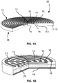
- Figure 1A schematically shows a SDD.
- a SDD is a silicon wafer (or part thereof) 10 , showing a volume of high purity, or at least showing little recombination sides, between a first side 11 and a second side 18 .
- Side 11 comprises the anode 16 and side 18 comprises the cathode 19. Electrodes of any electron/hole pairs generated in the volume between these two sides will drift to the anode and the holes to the cathode(s).
- Side 11 shows at a first side 11 a central electrode 12 forming the drain of a FET.
- An electrode 13 surrounding the central electrode forms the gate of the FET, and electrode 14 surrounding electrode 13 forms the source of the FET.
- the FET is shielded from the rest of the silicon wafer by a shield electrode 15 surrounding electrodes 12, 13 and 14, both laterally and 'inside' the wafer.
- the anode is connected to the gate of the FET (connection not shown in figure 1A ).
- a number of concentric electrodes 17-i Surrounding the anode a number of concentric electrodes 17-i are formed. The innermost of these concentric electrodes is connected to a voltage close to the anode voltage, the successive rings 17-i connected to voltages increasing from slightly above the anode voltage for the innermost of these electrodes to a voltage close to or equal to the cathode voltage for the outermost electrode.
- the ring electrodes 17-i cause a field inside the wafer that guides all the electrons from the electron/hole pairs to the anode, the anode being only a small structure and thus showing only a small capacitance with respect to the cathode. It is noted that, in working, a voltage difference is applied between the anode and the cathode. Hereby the capacitance of the anode with respect to the cathode is reduced. SDDs with an anode capacitance of 0.15 pF in working are commercially available.
- Figure 1B schematically shows a detail of the SDD shown in figure 1A .
- Figure 1B shows the part from the center until the anode.
- Side 18 is the side sensitive to radiation. Underneath this surface the sensitive volume 20 is shown.
- X-rays incident on the sensitive surface penetrate into the volume and generate in this volume a number of electron/hole pairs. The amount of electron/hole pairs depends on the energy of the photon. In normal operation the number of photons is such, that each event can be detected separately, and thus the number of electron/hole pairs per event, that is: per incident photon.
- Figure 2 schematically shows an electronic representation of a (part of a) SDD.
- the electronic representation shows the SDD used in a charge amplifier configuration.
- the parts within box 200 are part of the SDD wafer as shown in figure 1A and 1B , the other parts are external to the SDD wafer.
- the SDD comprises a cathode 201 and an anode 202, a FET 203 of which the gate is internally connected to the anode 202, a feedback capacitor 205 of which one side is connected to the anode 202, and a reset element in the form of diode 204 of which the cathode is connected to the anode 202.
- the SDD Connected to outputs of the SDD are its cathode, the source and drain of the FET, the side of the feedback capacitor not connected to the anode 202, and the anode of the reset diode.
- the external connections of the cathode 201 and the source of the FET are tied together to ground potential.
- the drain of the FET is connected to an amplifier 206.
- the output of the amplifier is connected to the feedback capacitor on the SDD and thus a charge amplifier is formed.
- Further reset logic 207 is connected to the output of the amplifier, which produces a pulse to the anode of the reset diode, as a result of which the SDD is reset.
- the detector can operate in so-called “continuous reset mode", in which the reset logic is not active, or not even present, and the drain/gate voltage of the FET generates a (voltage dependent) leakage current that compensates the induced (average) anode/cathode current
- the detector not shown, but necessary for operating the detector, are electronics for biasing the anode 202, the drain of the FET, and the concentric rings 17-i. It is noted that the voltages for the concentric rings can be derived from a resistive network integrated on the SDD between its anode and its cathode.
- the output of the amplifier is connected to further electronics and logic to determine the pulse height of the charge amplifier resulting from an incident photon.
- Figure 3 schematically shows the output signal of the SDD after the charge amplifier (206 in figure 2 ).
- the output signal typically a voltage
- steps are the result of a photon impinging on the diode.
- the height of the step varies, and is a measure for the energy of the photon.
- the noise on the signal between the steps with a peak-to-peak value 304. It is further shown that, when the signal exceeds a predetermined level, the charge amplifier is reset, resulting in a drop of the signal 305.
- FIG. 4 schematically shows the method according to the invention.
- the horizontal axis schematically shows the time axis
- the vertical axis schematically shows the amplitude of the signal.
- Box 400 shows the signal shown in figure 3 after filtering, in this case differentiating (high-pass filtered).
- the filtering lowers the dynamic range of the signal to slightly more than the dynamic range of one step (event), and thus lowers the constraint on the ADC sampling the signal.
- Box 402 shows sparsification of the (sampled) signal, resulting in a (temporally) compressed signal shown in box 404.
- This specific sparsification step - a filter operation that in this specific case compresses the signal temporally - results in an improved performance of the algorithm.
- Box 404 shows the compressed signal after the filtering action shown in box 402, the signal split in two streams: one stream going to box 406 and one to summing node 416.
- Box 410 shows the identical box as box 408 for convenience.
- Box 412 schematically shows the action of determining what data to use for the interpolation in the gap, find interpolated and/or extrapolated data using said data to use for the interpolation and a model, and then fill the gap with the thus found data.
- Box 414 shows an example of data retrieved by the action of box 412. This is thus an estimate of the noise contribution N(t) in the gap.
- Box 418 is the result of the subtraction, and represents an estimate of the pulse of box 404 minus the noise contribution shown in box 414.
- Box 420 schematically shows a filtering (integration) of the signal of box 418.
- Box 422 shows the resulting signal after the filtering of box 420. From this signal the step height can be derived.
- the method described here is based on a transformation of the input signal such that it can easily be split in a signal component (an x-ray detection component) and a stationary correlated noise component. This correlated noise component is subsequently used to improve the prediction of the energy content of the x-ray detection component.
- the key to and a novelty of the method described here is that the transformed signal is stationary. This in contrast with for example the earlier mentioned method described in EP2653892A1 pulse processor mentioned above.
- This allows us to "train" a fixed model (box 412) that is able to make a prediction, based on adjacent noise components, of the noise that is present in the x-ray detection components. Subtraction of the predicted noise component from the x-ray detection component improves the resolution of the x-ray spectrum.
- the model is trained based on system specific data, system imperfections that induce noise correlations are automatically compensated for.
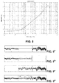
- Figure 5 schematically shows a Bode plot of an ARMA model, said model used to estimate the noise contribution in the gap.
- the ARMA model may be trained with the noise signal before the pulse occurred. Preferably it is trained on a-priori knowledge of the noise, most preferably off-line. It is noted that the training results (the model to be used) depend on noise properties of electronics, the dynamics of the signal (for example the width of the signal), etc. Therefore best results are obtained when a model is trained for each detector and using a signal as representative for a real signal as possible (or, better: with many samples as representative as possible).
- Figure 6 a -6 d schematically show how the signal can be interpolated.
- an estimate based on the data preceding the pulse (schematically shown in figure 6 b ) and an estimate based on data following the pulse (schematically shown in figure 6 c ) is determined, and using weight factors these two estimates are summed to form the estimate of the noise signal as shown in figure 6 d .
- ARMA modeling can thus result in a method where the model is constantly changed, and thus the model can trained for optimum performance.
- LOGI linear optimum gap interpolation
- LOGI uses a signal without events (steps), and defines a left part, a middle part and a right part.
- the middle part has a similar length (time or number of samples) as the part that is taken out in box 408 or fig. 6 a .
- the trick is now to find a solution that, using the left and the right parts, forms a reconstruction of the middle part that deviates as little as possible from the actual middle part. Training is best done using a large number of realistic samples.
- the (sampled) signal is denoted as a vector x 1..m , x m+1 .. k and x k+1 representing the left, middle and right interval (part/segment) respectively.
- ⁇ is the autocorrelation matrix of y
- Q is a ( m + n ) k matrix which relates each of the k unknown sample values to the available measurements contained in y.
- R n the autocorrelation function of x i
- the thus found estimators are defined (dependent) by the dynamics of the noise and the lengths of the known and unknown intervals.
Landscapes
- Physics & Mathematics (AREA)
- Health & Medical Sciences (AREA)
- Life Sciences & Earth Sciences (AREA)
- General Physics & Mathematics (AREA)
- High Energy & Nuclear Physics (AREA)
- Molecular Biology (AREA)
- Spectroscopy & Molecular Physics (AREA)
- Chemical & Material Sciences (AREA)
- Analytical Chemistry (AREA)
- Measurement Of Radiation (AREA)
Abstract
The invention relates to a method for analyzing an analogue signal (fig. 3, 400) comprising randomly spaced events (301, 302), the event having an event height, the method comprising:
• Converting the signal to a series of samples S(t), with t the moment of sampling, thereby forming a sampled, discrete time signal,
• Detecting the presence of an event, the event detected at t = T,
• Estimating the event height using a number of samples preceding the event and a number of samples following S(T),
the method further comprising:
• Using a model (412, fig. 5) to estimate a noise contribution N(t) for t = (T-Δ1) to t = (T+Δ2), the noise contribution derived from samples S(t) with t ≤ (T-Δ1) and/or samples S(t) with t ≥ (T+Δ2), with Δ1 and Δ2 predetermined or preset time periods, Δ1 having a value such that the event has a negligible contribution to samples taken before (T-Δ1) and Δ2 having a value such that the event has a negligible contribution to samples taken after (T+Δ2),
• Estimating the event height E by integrating the series of samples from (T-Δ1) to (T+Δ2) minus the noise contribution for said samples, 
• Converting the signal to a series of samples S(t), with t the moment of sampling, thereby forming a sampled, discrete time signal,
• Detecting the presence of an event, the event detected at t = T,
• Estimating the event height using a number of samples preceding the event and a number of samples following S(T),
the method further comprising:
• Using a model (412, fig. 5) to estimate a noise contribution N(t) for t = (T-Δ1) to t = (T+Δ2), the noise contribution derived from samples S(t) with t ≤ (T-Δ1) and/or samples S(t) with t ≥ (T+Δ2), with Δ1 and Δ2 predetermined or preset time periods, Δ1 having a value such that the event has a negligible contribution to samples taken before (T-Δ1) and Δ2 having a value such that the event has a negligible contribution to samples taken after (T+Δ2),
• Estimating the event height E by integrating the series of samples from (T-Δ1) to (T+Δ2) minus the noise contribution for said samples,
In an important aspect of the invention, the sampled signal is subjected to a sparsification operation that causes said event to be temporally compressed.
This method is particularly useful for X-ray detectors, such as Silicon Drift Detectors, used in a SEM. By estimating the noise contribution to the signal, the step height is estimated with improved accuracy. The invention further describes several methods to be used as a model.
Description
- The invention relates to a method for analyzing an analogue signal comprising randomly spaced events, the method comprising:
- converting the signal to a series of samples S(t), with t the moment of sampling, thereby forming a sampled, discrete time signal,
- detecting the presence of an event, the event detected at t = T,
- estimating the event height using a number of samples preceding the event and a number of samples following S(T).
- The invention further relates to an apparatus equipped to perform the method.
- When an X-ray photon or an electron hit a semiconductor detector, a number of electron-hole pairs are generated in the detector. By biasing the detector, either by an externally applied voltage or by a built-in internal field due to doping of the semiconductor material, the electrons are attracted to the anode or the holes are attracted to the cathode. This results in a pulse. This pulse can be detected, preferably after first amplifying the signal, for example with a FET amplifier. By now detecting the pulse height the energy of the X-ray photon or electron can be determined. As known to the skilled person the energy of an X-ray photon is an indication of the element that emitted said photon.
- European patent application no.
EP2653892A1 describes a method for analyzing the signal of a Silicon Drift Detector (SDD) for X-ray detection in a charged particle apparatus. The signal is analyzed to detect steps, estimating the level of the signal before each step and after each step and using these estimates estimating the step height by subtracting the two levels from each other. The level before each step is estimated by averaging (integrating) the signal over time: the longer the averaging, the lower the variance in the signal. However, the maximum integration time is limited to avoid noise contributions stemming from low-frequency noise, leakage, etc. - It is noted that the steps are the result of the (analogue) integration of pulses by the FET amplifier.
- Another such method is known from US patent no.
US 7,966,155B2 . - This US patent a method comprising converting the signal to a series of samples, detecting the presence of a step, estimate the signal level before the step and after the step by filtering the signal by using a switchable integrator, and estimating the step height by subtracting the two levels from each other. The integration time of the two integrators is selectable dependent on the time period between said pulse and the preceding and following pulses.
- It is known that an X-ray photon or an electron can be detected in, for example, a semiconductor device (assuming the photon or electron is sufficiently energetic). Both the method described in the EP patent application and in the US patent can be used to determine the energy of an X-ray photon detected in a semiconductor device (for example a SDD) or a Geiger-Müller device, or to detect the energy of an electron detected in a semiconductor detector.
- Both the method described in the EP patent application and in the US patent try to determine the signal levels before and after an event as good as possible. If the time between events is small, the variance of the estimates of the signal level between the events is high due to signal-to-noise problems. Noise sources of a signal of a (FET) amplifier can be: series noise, parallel noise and 1/f at the amplifier input, and in the case of X-ray and electron detectors Fano noise due to the uncertainty of the number of electrons generated in an event (incoming photon or electron).
- Both the method described in the EP patent application and in the US patent give a less reliable value for the event height when the time between events decreases. For both methods operating at high count rate is therefore coupled to less reliable values for the event height.
- There is a need for a method allowing more reliable estimation of the event height at a high count rate.
- To that end the method according to the invention is characterized in that
- a model is used to estimate a noise contribution N(t) for t = (T-Δ1) to t = (T+Δ2), the noise contribution derived from samples S(t) with t ≤ (T-Δ1) and/or samples S(t) with t ≥ (T+Δ2), with Δ1 and Δ2 predetermined or preset time periods, Δ1 having a value such that the event has a negligible contribution to samples taken before (T-Δ1) and Δ2 having a value such that the event has a negligible contribution to samples taken after (T+Δ2),
- the event height E is estimated by integrating the series of samples from (T-Δ1) to (T+Δ2) minus the noise contribution for said samples,

- The invention is based on the insight that the noise during the time interval that the event occurs can, at least partly, be estimated from samples following and/or preceding the event. By integrating the signal over the period that the event occurs and subtracting the noise from it, a more accurate estimate of the event height is made. In other words: the invention is based on the (inventive) use of the correlation in the noise.
- A non-exhaustive list of signal sources is:
- a silicon x-ray detector (such as a PIN diode or a SSD) for detecting X-rays,
- an electron detector for use in a particle-optical apparatus,
- an acoustic detector such as a microphone for detecting, for example, sonic 'booms'
- a hydrophone for detecting, for example, 'pings' from electronic devices such as the black boxes of airplanes,
- a seismic detector,
- a superconducting bolometer for detecting radiation,
- a scintillation detector.
- The signal may be sampled by a sample & hold device to be processed in a device using a bucket-brigade-delay-line, or by passing it through an analogue-digital converter for processing in the digital domain.
- Before the signal is sampled, it may be filtered. By, for example, differentiating the signal, the dynamic range of the signal to be sampled is reduced; as a result, an improved signal representation can be achieved. By, for example, integrating, aliasing is avoided. Such manipulation (e.g. with an analogue filter) prior to sampling can be referred to as signal "shaping".
- In a particularly advantageous embodiment of the invention, after the signal is converted to a series of samples, it is subjected to a sparsification operation that causes said event to be temporally compressed. By compressing the event in this manner, it will span/occupy fewer samples (sample windows), allowing a more accurate estimation of noise behavior within its boundaries. This aspect of this invention is, for example, illustrated in
Figure 4 , in which a suitable linear (energy-proportional) filtering operation is depicted in block 402 - which may, for instance, reduce the temporal span of the event from a width of ca. 1000 sample windows to a width of the order of ca. 20 sample windows. It should be noted that such sparsification is the antithesis of event "stretching", e.g. as performed inUS 5,307,299 , in which the event is converted into an extended step, with the attendant problem of "random walk" in the associated noise. It is also different to the approach inWO 2003/040757 A2 , for example, which processes the event "as is", without attempting to compress or stretch it. One way to achieve the inventive sparsification is to filter the incoming signal with a discrete-time transformation of the continuous-time transfer function:


block 404 ofFigure 4 , in which the original pulse event has been compressed into a form resembling a Dirac delta function. This is advantageous in that: - The number of samples to be estimated (within the pulse) is reduced;
- Concurrently, more samples become available for estimation purposes between subsequent pulses.
- The event may, for example, be a pulse in the signal, or a step on the signal (e.g. a flank of a block), or an edge followed by a decay time. If it is known that the signal is a convoluted signal, the signal may be deconvoluted either before sampling (using for example electrical integrators and/or differentiators) or by passing the sampled signal through a filter.
- The noise prediction model may comprise: linear interpolation, extrapolation, autoregressive modeling (AR modeling), ARMA modeling, or a method based on Linear Optimum Gap Interpolation (LOGI).
- The modeling may be a modeling using a fixed set of parameters (for example using fixed values for Δ1 and Δ2), or may use a variable set of parameters, for example using values for Δ1 and Δ2 that depend on the time of earlier noise (the signal before t = T).
- It is noted that the number of samples may depend on the moment of time that a previous or following event occurs: when the period is small, only a small number of samples is used, while for long periods the number of samples may be limited to a maximum number.
- In an aspect of the invention an apparatus is equipped with an X-ray or secondary electron detector and a programmable processor for processing the data of said detector, the processor programmed to perform any of the preceding methods.
- This aspect describes a charged particle apparatus, for example a Scanning Electron Microscope (SEM) or an apparatus using an X-ray source, equipped with, for example, a SDD and a processor for processing the signal produced by the detector.
- In an embodiment the charged particle apparatus in which a sample is irradiated is an apparatus where a focused beam of energetic electrons irradiates the sample, in response to which X-rays and/or secondary electrons are emitted by the sample to be detected by the detector.
- It is well-known that X-ray analysis of a sample can be done in a SEM using a beam energy of, for example, 10 keV or more.
- The invention is now elucidated using figures in which identical reference numerals refer to corresponding features.
- To that end:
-
figure 1A schematically shows a SDD; -
figure 1B schematically shows a detail offigure 1A ; -
figure 2 schematically shows an electrical scheme of a FET amplifier part of the SDD; -
figure 3 schematically shows the output signal of the SDD after the charge amplifier; -
figure 4 schematically shows a workflow according to the method; -
figure 5 schematically shows a Bode plot of an ARMA model; and -
figure 6 a-6d schematically show how the signal can be interpolated. -
Figure 1A schematically shows a SDD. - A SDD is a silicon wafer (or part thereof) 10, showing a volume of high purity, or at least showing little recombination sides, between a
first side 11 and asecond side 18.Side 11 comprises theanode 16 andside 18 comprises thecathode 19. Electrodes of any electron/hole pairs generated in the volume between these two sides will drift to the anode and the holes to the cathode(s).Side 11 shows at a first side 11 acentral electrode 12 forming the drain of a FET. Anelectrode 13 surrounding the central electrode forms the gate of the FET, andelectrode 14 surroundingelectrode 13 forms the source of the FET. The FET is shielded from the rest of the silicon wafer by ashield electrode 15 surroundingelectrodes figure 1A ). - Surrounding the anode a number of concentric electrodes 17-i are formed. The innermost of these concentric electrodes is connected to a voltage close to the anode voltage, the successive rings 17-i connected to voltages increasing from slightly above the anode voltage for the innermost of these electrodes to a voltage close to or equal to the cathode voltage for the outermost electrode.
The ring electrodes 17-i cause a field inside the wafer that guides all the electrons from the electron/hole pairs to the anode, the anode being only a small structure and thus showing only a small capacitance with respect to the cathode.
It is noted that, in working, a voltage difference is applied between the anode and the cathode. Hereby the capacitance of the anode with respect to the cathode is reduced. SDDs with an anode capacitance of 0.15 pF in working are commercially available. -
Figure 1B schematically shows a detail of the SDD shown infigure 1A .
Figure 1B shows the part from the center until the anode. Here the connection betweenanode 16 and the gate of the FET is schematically shown as ametallization 21Side 18 is the side sensitive to radiation. Underneath this surface thesensitive volume 20 is shown. X-rays incident on the sensitive surface penetrate into the volume and generate in this volume a number of electron/hole pairs. The amount of electron/hole pairs depends on the energy of the photon. In normal operation the number of photons is such, that each event can be detected separately, and thus the number of electron/hole pairs per event, that is: per incident photon.
Charge accumulates on the anode forcing the voltage of the anode to become more and more negative (with respect to the cathode) until a reset of the anode is caused by resetting the anode with, for example, a reset diode (not shown).
Alternatively leakage current from the drain of the FET to its gate can be used to compensate for the average charge accumulation. - It is noted that often a feedback capacitor is integrated on the SDD, connecting the anode to an output, but that this capacitor can also be placed outside the SDD.
-
Figure 2 schematically shows an electronic representation of a (part of a) SDD. - The electronic representation shows the SDD used in a charge amplifier configuration. The parts within
box 200 are part of the SDD wafer as shown infigure 1A and 1B , the other parts are external to the SDD wafer.
The SDD comprises acathode 201 and ananode 202, aFET 203 of which the gate is internally connected to theanode 202, afeedback capacitor 205 of which one side is connected to theanode 202, and a reset element in the form ofdiode 204 of which the cathode is connected to theanode 202. Connected to outputs of the SDD are its cathode, the source and drain of the FET, the side of the feedback capacitor not connected to theanode 202, and the anode of the reset diode. The external connections of thecathode 201 and the source of the FET are tied together to ground potential. The drain of the FET is connected to anamplifier 206. The output of the amplifier is connected to the feedback capacitor on the SDD and thus a charge amplifier is formed.Further reset logic 207 is connected to the output of the amplifier, which produces a pulse to the anode of the reset diode, as a result of which the SDD is reset. - It is mentioned that, when the FET is used as a source follower, and where the voltage between drain and gate Vdg varies, the detector can operate in so-called "continuous reset mode", in which the reset logic is not active, or not even present, and the drain/gate voltage of the FET generates a (voltage dependent) leakage current that compensates the induced (average) anode/cathode current
- Not shown, but necessary for operating the detector, are electronics for biasing the
anode 202, the drain of the FET, and the concentric rings 17-i. It is noted that the voltages for the concentric rings can be derived from a resistive network integrated on the SDD between its anode and its cathode. - It is noted that the output of the amplifier is connected to further electronics and logic to determine the pulse height of the charge amplifier resulting from an incident photon.
- In Application note AN-SDD-003: Amptek Silicon Drift Detectors (http://www.amptek.com/pdf/ansdd3.pdf), more specifically in figure 10 and associated text, the noise of this circuit is discussed.
-
Figure 3 schematically shows the output signal of the SDD after the charge amplifier (206 infigure 2 ). - The output signal, typically a voltage, shows a number of steps, for
example steps example interval 303. These steps are the result of a photon impinging on the diode. The height of the step varies, and is a measure for the energy of the photon. Clearly visible is the noise on the signal between the steps, with a peak-to-peak value 304. It is further shown that, when the signal exceeds a predetermined level, the charge amplifier is reset, resulting in a drop of thesignal 305. -
Figure 4 schematically shows the method according to the invention. - In the boxes showing horizontal and vertical axis, the horizontal axis schematically shows the time axis, the vertical axis schematically shows the amplitude of the signal.
-
Box 400 shows the signal shown infigure 3 after filtering, in this case differentiating (high-pass filtered). The filtering lowers the dynamic range of the signal to slightly more than the dynamic range of one step (event), and thus lowers the constraint on the ADC sampling the signal. -
Box 402 shows sparsification of the (sampled) signal, resulting in a (temporally) compressed signal shown inbox 404. This specific sparsification step - a filter operation that in this specific case compresses the signal temporally - results in an improved performance of the algorithm. -
Box 404 shows the compressed signal after the filtering action shown inbox 402, the signal split in two streams: one stream going to box 406 and one to summingnode 416. In this compressed signal the pulse is clearly detectable, detected at moment t = T. -
Box 406 schematically shows the action where part of the data surrounding the pulse, the data from t = (T-Δ1) to t = (T+Δ2), is deleted. -
Box 408 schematically shows the data stream after deleting the data from t = (T-Δ1) to t = (T+Δ2). It is noted that this data only comprises noise, as any signal to which the pulse significantly contributes is deleted (indicated by the scissors of box 406). -
Box 410 shows the identical box asbox 408 for convenience. -
Box 412 schematically shows the action of determining what data to use for the interpolation in the gap, find interpolated and/or extrapolated data using said data to use for the interpolation and a model, and then fill the gap with the thus found data. This box schematically shows the result of an interpolation action based on a model using data present in the data S(t) using samples sampled before t = (T-Δ1) and/or after t = (T+Δ2). -
Box 414 shows an example of data retrieved by the action ofbox 412. This is thus an estimate of the noise contribution N(t) in the gap. -
Box 416 shows that the noise contribution N(t) is subtracted from the signal S(t) for t = (T-Δ1) to t = (T+Δ2). -
Box 418 is the result of the subtraction, and represents an estimate of the pulse ofbox 404 minus the noise contribution shown inbox 414. -
Box 420 schematically shows a filtering (integration) of the signal ofbox 418. -
Box 422 shows the resulting signal after the filtering ofbox 420. From this signal the step height can be derived. - The method described here is based on a transformation of the input signal such that it can easily be split in a signal component (an x-ray detection component) and a stationary correlated noise component. This correlated noise component is subsequently used to improve the prediction of the energy content of the x-ray detection component.
- The key to and a novelty of the method described here is that the transformed signal is stationary. This in contrast with for example the earlier mentioned method described in
EP2653892A1 pulse processor mentioned above. This allows us to "train" a fixed model (box 412) that is able to make a prediction, based on adjacent noise components, of the noise that is present in the x-ray detection components. Subtraction of the predicted noise component from the x-ray detection component improves the resolution of the x-ray spectrum. We note that, because the model is trained based on system specific data, system imperfections that induce noise correlations are automatically compensated for. -
Figure 5 schematically shows a Bode plot of an ARMA model, said model used to estimate the noise contribution in the gap. The ARMA model may be trained with the noise signal before the pulse occurred. Preferably it is trained on a-priori knowledge of the noise, most preferably off-line. It is noted that the training results (the model to be used) depend on noise properties of electronics, the dynamics of the signal (for example the width of the signal), etc. Therefore best results are obtained when a model is trained for each detector and using a signal as representative for a real signal as possible (or, better: with many samples as representative as possible). -
Figure 6 a-6d schematically show how the signal can be interpolated. - Using this ARMA model and the signal surrounding the gap (shown in
figure 6 a), an estimate based on the data preceding the pulse (schematically shown infigure 6 b) and an estimate based on data following the pulse (schematically shown infigure 6 c) is determined, and using weight factors these two estimates are summed to form the estimate of the noise signal as shown infigure 6 d. - It is noted that the before mentioned ARMA modeling can thus result in a method where the model is constantly changed, and thus the model can trained for optimum performance.
- It is further noted that the before mentioned ARMA modeling is only one example of many implementation that can be used.
- Best results are obtained when the optimum model is used for the noise. This is best done by "training" the model until said optimum (or a solution close to that) is found. Inventors found a training method that was of special interest for this invention: the linear optimum gap interpolation (LOGI). LOGI uses a signal without events (steps), and defines a left part, a middle part and a right part. The middle part has a similar length (time or number of samples) as the part that is taken out in
box 408 orfig. 6 a. The trick is now to find a solution that, using the left and the right parts, forms a reconstruction of the middle part that deviates as little as possible from the actual middle part. Training is best done using a large number of realistic samples. - Mathematically this is expressed as follows:
- Assume the (sampled) signal is denoted as a vector x1..m, xm+1..k and xk+1 representing the left, middle and right interval (part/segment) respectively. Denoting vector y as the known (concatenated) intervals, and s the unknown interval, the optimum gap interpolator W in the least mean square sense is an (m + n) · k matrix given by minimizing

- Differentiation of this equation with respect to the elements of W and equating to zero, the solution to this problem satisfies:

- It can be seen that Σ is the autocorrelation matrix of y, and Q is a (m + n) k matrix which relates each of the k unknown sample values to the available measurements contained in y. With Rn the autocorrelation function of xi, the structure of the two matrices then expands to:


- The thus found estimators are defined (dependent) by the dynamics of the noise and the lengths of the known and unknown intervals.
- Using the matrix Σ for the left part of the formula, and the matrix Q for the right part, this reduces to

- The interpolation for pulse (event) j is given (predicted) by:

- It is noted that, although the memory requirements for LOGI are much higher than the requirements for ARMA modelling, the required memory can be dramatically reduced by sparsification of the data.
- It is further noted that other methods/models that can be used for the interpolation are described in handbooks such as:
- Box, G. et al.,"Time Series Analysis: Forecasting & Control", 4th edition, Wiley, ISBN. ISBN: 978-0-470-27284-8.
- Hyndman, R. et al., (2014). "Forecasting: principles and practice", OTexts (October 17, 2013) ISBN-10: 0987507109.
- We claim as follows:
Claims (13)
- A method for analyzing an analogue signal (fig. 3, 400) comprising randomly spaced events (301, 302), the event having an event height, the method comprising:• Converting the signal to a series of samples S(t), with t the moment of sampling, thereby forming a sampled, discrete time signal,• Detecting the presence of an event, the event detected at t = T,• Estimating the event height using a number of samples preceding the event and a number of samples following S(T),Characterized in that the method further comprises• Using a model (412, fig. 5) to estimate a noise contribution N(t) for t = (T-Δ1) to t = (T+Δ2), the noise contribution derived from samples S(t) with t ≤ (T-Δ1) and/or samples S(t) with t ≥ (T+Δ2), with Δ1 and Δ2 predetermined or preset time periods, Δ1 having a value such that the event has a negligible contribution to samples taken before (T-Δ1) and Δ2 having a value such that the event has a negligible contribution to samples taken after (T+Δ2),• Estimating the event height E by integrating the series of samples from (T-Δ1) to (T+Δ2) minus the noise contribution for said samples,

- The method of claim 1 in which the event is a step (301, 302) or a pulse (400).
- The method of claim 1 or 2 in which, the sampled signal is subjected to a sparsification operation that causes said event to be temporally compressed.
- The method of any of the preceding claims in which, before the signal is converted to a series of samples, the signal is filtered.
- The method of claim 4 in which the filtering of the analogue signal comprises differentiating and/or integrating.
- The method of any of the preceding claims in which the conversion of the signal comprises an analogue-to-digital conversion.
- The method of any of the preceding claims in which the model (412) to predict noise comprises interpolation using S(T-Δ1) and S(T+Δ2), interpolation using more than two points, autoregressive (AR) modeling, ARMA modeling using samples S(t) for t ≤ (T-Δ1) and/or t ≥ (T+Δ2), or Linear Optimum Gap Interpolation, or combinations thereof.
- The method of claim 7 in which the model (412) uses parameters, and the parameters are changed according to the signal preceding the moment of the pulse, t = T.
- The method of any of the preceding claims in which Δ1 is based on the time between the event and an earlier event and/or Δ2 is determined based on the time between the event and a following event and/or form of the event.
- The method of any of the preceding claims in which the randomly spaced events are steps resulting from the integration of randomly spaced pulses.
- The method of any of the preceding claims in which the signal is the signal of a semiconductor X-ray detector, a Silicon Drift Detector (fig 1A), an acoustic detector, a hydrophone, a scintillator detector or a superconducting bolometer.
- An apparatus equipped with an X-ray or secondary electron detector and a programmable processor for processing the data of said detector, the processor programmed to perform any of the preceding methods.
- The apparatus of claim 12 in which a sample is irradiated with a focused beam of energetic electrons, in response to which X-rays and/or secondary electrons are emitted by the sample to be detected by the detector.
Priority Applications (1)
| Application Number | Priority Date | Filing Date | Title |
|---|---|---|---|
| EP16156848.0A EP3062126A1 (en) | 2015-02-26 | 2016-02-23 | Pulse processing |
Applications Claiming Priority (2)
| Application Number | Priority Date | Filing Date | Title |
|---|---|---|---|
| EP15156716.1A EP3062125A1 (en) | 2015-02-26 | 2015-02-26 | Pulse processing |
| EP16156848.0A EP3062126A1 (en) | 2015-02-26 | 2016-02-23 | Pulse processing |
Publications (1)
| Publication Number | Publication Date |
|---|---|
| EP3062126A1 true EP3062126A1 (en) | 2016-08-31 |
Family
ID=52574085
Family Applications (2)
| Application Number | Title | Priority Date | Filing Date |
|---|---|---|---|
| EP15156716.1A Withdrawn EP3062125A1 (en) | 2015-02-26 | 2015-02-26 | Pulse processing |
| EP16156848.0A Withdrawn EP3062126A1 (en) | 2015-02-26 | 2016-02-23 | Pulse processing |
Family Applications Before (1)
| Application Number | Title | Priority Date | Filing Date |
|---|---|---|---|
| EP15156716.1A Withdrawn EP3062125A1 (en) | 2015-02-26 | 2015-02-26 | Pulse processing |
Country Status (4)
| Country | Link |
|---|---|
| US (2) | US10403470B2 (en) |
| EP (2) | EP3062125A1 (en) |
| JP (1) | JP6685764B2 (en) |
| CN (1) | CN105929436B (en) |
Cited By (1)
| Publication number | Priority date | Publication date | Assignee | Title |
|---|---|---|---|---|
| US11274965B2 (en) | 2020-02-10 | 2022-03-15 | International Business Machines Corporation | Noise model-based converter with signal steps based on uncertainty |
Families Citing this family (3)
| Publication number | Priority date | Publication date | Assignee | Title |
|---|---|---|---|---|
| US10122946B2 (en) | 2015-11-11 | 2018-11-06 | Fei Company | Method for detecting particulate radiation |
| EP4627607A2 (en) * | 2022-12-06 | 2025-10-08 | Guardion, Inc. | Charge sensor |
| CN116299629B (en) * | 2022-12-30 | 2026-06-02 | 合肥锐世数字科技有限公司 | Methods, apparatus, equipment and storage media for processing flicker pulses |
Citations (7)
| Publication number | Priority date | Publication date | Assignee | Title |
|---|---|---|---|---|
| US5307299A (en) | 1991-12-09 | 1994-04-26 | Forschungszentrum Julich Gmbh | Circuit arrangement for the digital processing of semiconductor detector signals |
| US5349193A (en) * | 1993-05-20 | 1994-09-20 | Princeton Gamma Tech, Inc. | Highly sensitive nuclear spectrometer apparatus and method |
| WO2003040757A2 (en) | 2001-10-16 | 2003-05-15 | Board Of Regents, The University Of Texas System | Method and apparatus to prevent signal pile-up |
| US20060029279A1 (en) * | 2004-08-09 | 2006-02-09 | Donoho David L | Method and apparatus for compressed sensing |
| US7966155B2 (en) | 2004-06-04 | 2011-06-21 | William K. Warburton | Method and apparatus for improving detection limits in x-ray and nuclear spectroscopy systems |
| EP2653892A2 (en) | 2012-04-19 | 2013-10-23 | Fei Company | Method for analyzing an EDS signal |
| US20140114596A1 (en) * | 2012-10-22 | 2014-04-24 | Mitsubishi Electric Corporation | Radiation measuring apparatus |
Family Cites Families (7)
| Publication number | Priority date | Publication date | Assignee | Title |
|---|---|---|---|---|
| JP3688160B2 (en) * | 1999-09-17 | 2005-08-24 | 株式会社日立製作所 | Scanning electron microscope |
| US7230239B2 (en) * | 2003-06-13 | 2007-06-12 | Hitachi High-Technologies Corporation | Apparatus for inspecting three dimensional shape of a specimen and method of watching an etching process using the same |
| FR2888644B1 (en) * | 2005-07-12 | 2007-09-14 | Commissariat Energie Atomique | IMPROVED TREATMENT OF A REPRESENTATIVE RADIATION SIGNAL |
| JP5455904B2 (en) * | 2007-08-03 | 2014-03-26 | パルセータ,エルエルシー | Pile-up detection method in energy dispersive radiation spectroscopic analysis system, pulse processor for executing the method, and energy dispersive radiation spectroscopic analysis system for detecting pile-up |
| US20100010780A1 (en) * | 2008-07-10 | 2010-01-14 | The Hong Kong Polytechnic University | Method for signal denoising using continuous wavelet transform |
| JP5595054B2 (en) * | 2010-01-29 | 2014-09-24 | 株式会社日立ハイテクサイエンス | Electron microscope and sample analysis method |
| EP2958130A1 (en) * | 2014-06-18 | 2015-12-23 | Fei Company | Mathematical image assembly in a scanning-type microscope |
-
2015
- 2015-02-26 EP EP15156716.1A patent/EP3062125A1/en not_active Withdrawn
-
2016
- 2016-02-23 EP EP16156848.0A patent/EP3062126A1/en not_active Withdrawn
- 2016-02-23 JP JP2016031718A patent/JP6685764B2/en active Active
- 2016-02-25 US US15/053,898 patent/US10403470B2/en active Active
- 2016-02-26 CN CN201610106051.1A patent/CN105929436B/en active Active
-
2019
- 2019-07-25 US US16/522,308 patent/US10692691B2/en active Active
Patent Citations (7)
| Publication number | Priority date | Publication date | Assignee | Title |
|---|---|---|---|---|
| US5307299A (en) | 1991-12-09 | 1994-04-26 | Forschungszentrum Julich Gmbh | Circuit arrangement for the digital processing of semiconductor detector signals |
| US5349193A (en) * | 1993-05-20 | 1994-09-20 | Princeton Gamma Tech, Inc. | Highly sensitive nuclear spectrometer apparatus and method |
| WO2003040757A2 (en) | 2001-10-16 | 2003-05-15 | Board Of Regents, The University Of Texas System | Method and apparatus to prevent signal pile-up |
| US7966155B2 (en) | 2004-06-04 | 2011-06-21 | William K. Warburton | Method and apparatus for improving detection limits in x-ray and nuclear spectroscopy systems |
| US20060029279A1 (en) * | 2004-08-09 | 2006-02-09 | Donoho David L | Method and apparatus for compressed sensing |
| EP2653892A2 (en) | 2012-04-19 | 2013-10-23 | Fei Company | Method for analyzing an EDS signal |
| US20140114596A1 (en) * | 2012-10-22 | 2014-04-24 | Mitsubishi Electric Corporation | Radiation measuring apparatus |
Non-Patent Citations (3)
| Title |
|---|
| BOX, G. ET AL.: "Time Series Analysis: Forecasting & Control", WILEY |
| HYNDMAN, R. ET AL.: "OTexts", 2014, article "Forecasting: principles and practice" |
| MICHAEL PAQUETTE ET AL: "Comparison of sampling strategies and sparsifying transforms to improve compressed sensing diffusion spectrum imaging", MAGNETIC RESONANCE IN MEDICINE., vol. 73, no. 1, 1 January 2015 (2015-01-01), US, pages 401 - 416, XP055281817, ISSN: 0740-3194, DOI: 10.1002/mrm.25093 * |
Cited By (1)
| Publication number | Priority date | Publication date | Assignee | Title |
|---|---|---|---|---|
| US11274965B2 (en) | 2020-02-10 | 2022-03-15 | International Business Machines Corporation | Noise model-based converter with signal steps based on uncertainty |
Also Published As
| Publication number | Publication date |
|---|---|
| US20160254119A1 (en) | 2016-09-01 |
| US10692691B2 (en) | 2020-06-23 |
| CN105929436A (en) | 2016-09-07 |
| US20190362932A1 (en) | 2019-11-28 |
| CN105929436B (en) | 2020-06-09 |
| JP2016161574A (en) | 2016-09-05 |
| EP3062125A1 (en) | 2016-08-31 |
| JP6685764B2 (en) | 2020-04-22 |
| US10403470B2 (en) | 2019-09-03 |
Similar Documents
| Publication | Publication Date | Title |
|---|---|---|
| US10692691B2 (en) | Pulse processing | |
| CN103376456B (en) | Method for analyzing EDS signals | |
| JP5815532B2 (en) | Device for processing signals supplied by radiation detectors | |
| JP2014529723A (en) | Method and apparatus for identifying pulses in detector output data | |
| JP7041079B2 (en) | Improved photon counting in spectral radiation detectors | |
| JP2013513788A (en) | Method and device for recognizing materials using transmission functions | |
| US9689994B2 (en) | Method for correcting the stacking phenomenon applied to X-ray spectrums acquired using a spectrometric sensor | |
| US10641909B2 (en) | Method for processing a pulse generated by a detector of ionizing radiation | |
| US20160363545A1 (en) | Method for measuring the effective atomic number of a material | |
| Pullia et al. | Time-domain simulation of electronic noises | |
| JP2011002371A (en) | Seismic intensity estimation method and device | |
| JP2014085171A (en) | Radiation measurement instrument | |
| JP7685998B2 (en) | Compensation for polarization effects in photon-counting detectors. | |
| WO2015186202A1 (en) | Scanning electron microscope device | |
| US7345285B2 (en) | Spectra acquisition system with threshold adaptation integrator | |
| Murray et al. | A low power, high count rate radiation detection chip using a current subtraction technique | |
| Elter et al. | Performance of Higher Order Campbell methods, Part II: calibration and experimental application | |
| Moline et al. | Auto-adaptive trigger and pulse extraction for digital processing in nuclear instrumentation | |
| Gilard et al. | Statistical analysis of random telegraph signal maximum transition amplitudes in an irradiated CMOS image sensor | |
| Tanguay et al. | Extension of cascaded systems analysis to single-photon-counting x-ray detectors | |
| CN113031045A (en) | Method for determining the offset of a pixel of a pixelated detector influencing ionizing radiation | |
| JPH0619455B2 (en) | Radiation measuring device | |
| Sopczak et al. | Measurements of charge transfer inefficiency in a CCD with high-speed column parallel readout | |
| US20130147648A1 (en) | Asynchronous digitisation of transient signals from radiation detectors | |
| Souza et al. | Performance study for a set of BLUE based Filters applied to amplitude estimation using as a reference the single photoelectron signal of the ν-Angra Experiment |
Legal Events
| Date | Code | Title | Description |
|---|---|---|---|
| PUAI | Public reference made under article 153(3) epc to a published international application that has entered the european phase |
Free format text: ORIGINAL CODE: 0009012 |
|
| AK | Designated contracting states |
Kind code of ref document: A1 Designated state(s): AL AT BE BG CH CY CZ DE DK EE ES FI FR GB GR HR HU IE IS IT LI LT LU LV MC MK MT NL NO PL PT RO RS SE SI SK SM TR |
|
| AX | Request for extension of the european patent |
Extension state: BA ME |
|
| STAA | Information on the status of an ep patent application or granted ep patent |
Free format text: STATUS: THE APPLICATION IS DEEMED TO BE WITHDRAWN |
|
| 18D | Application deemed to be withdrawn |
Effective date: 20170301 |