EP3059681A1 - Signal count reduction between semiconductor dies assembled in wafer-level package - Google Patents
Signal count reduction between semiconductor dies assembled in wafer-level package Download PDFInfo
- Publication number
- EP3059681A1 EP3059681A1 EP16155812.7A EP16155812A EP3059681A1 EP 3059681 A1 EP3059681 A1 EP 3059681A1 EP 16155812 A EP16155812 A EP 16155812A EP 3059681 A1 EP3059681 A1 EP 3059681A1
- Authority
- EP
- European Patent Office
- Prior art keywords
- signal
- semiconductor die
- wafer
- assembled
- level package
- Prior art date
- Legal status (The legal status is an assumption and is not a legal conclusion. Google has not performed a legal analysis and makes no representation as to the accuracy of the status listed.)
- Withdrawn
Links
Images





Classifications
-
- G—PHYSICS
- G06—COMPUTING OR CALCULATING; COUNTING
- G06F—ELECTRIC DIGITAL DATA PROCESSING
- G06F13/00—Interconnection of, or transfer of information or other signals between, memories, input/output devices or central processing units
- G06F13/38—Information transfer, e.g. on bus
- G06F13/40—Bus structure
- G06F13/4063—Device-to-bus coupling
- G06F13/4068—Electrical coupling
-
- H—ELECTRICITY
- H10—SEMICONDUCTOR DEVICES; ELECTRIC SOLID-STATE DEVICES NOT OTHERWISE PROVIDED FOR
- H10D—INORGANIC ELECTRIC SEMICONDUCTOR DEVICES
- H10D89/00—Aspects of integrated devices not covered by groups H10D84/00 - H10D88/00
- H10D89/10—Integrated device layouts
-
- G—PHYSICS
- G06—COMPUTING OR CALCULATING; COUNTING
- G06F—ELECTRIC DIGITAL DATA PROCESSING
- G06F13/00—Interconnection of, or transfer of information or other signals between, memories, input/output devices or central processing units
- G06F13/14—Handling requests for interconnection or transfer
- G06F13/36—Handling requests for interconnection or transfer for access to common bus or bus system
- G06F13/362—Handling requests for interconnection or transfer for access to common bus or bus system with centralised access control
- G06F13/3625—Handling requests for interconnection or transfer for access to common bus or bus system with centralised access control using a time dependent access
-
- G—PHYSICS
- G06—COMPUTING OR CALCULATING; COUNTING
- G06F—ELECTRIC DIGITAL DATA PROCESSING
- G06F13/00—Interconnection of, or transfer of information or other signals between, memories, input/output devices or central processing units
- G06F13/14—Handling requests for interconnection or transfer
- G06F13/36—Handling requests for interconnection or transfer for access to common bus or bus system
- G06F13/362—Handling requests for interconnection or transfer for access to common bus or bus system with centralised access control
- G06F13/364—Handling requests for interconnection or transfer for access to common bus or bus system with centralised access control using independent requests or grants, e.g. using separated request and grant lines
-
- G—PHYSICS
- G06—COMPUTING OR CALCULATING; COUNTING
- G06F—ELECTRIC DIGITAL DATA PROCESSING
- G06F13/00—Interconnection of, or transfer of information or other signals between, memories, input/output devices or central processing units
- G06F13/38—Information transfer, e.g. on bus
- G06F13/42—Bus transfer protocol, e.g. handshake; Synchronisation
- G06F13/4282—Bus transfer protocol, e.g. handshake; Synchronisation on a serial bus, e.g. I2C bus, SPI bus
-
- H—ELECTRICITY
- H10—SEMICONDUCTOR DEVICES; ELECTRIC SOLID-STATE DEVICES NOT OTHERWISE PROVIDED FOR
- H10W—GENERIC PACKAGES, INTERCONNECTIONS, CONNECTORS OR OTHER CONSTRUCTIONAL DETAILS OF DEVICES COVERED BY CLASS H10
- H10W70/00—Package substrates; Interposers; Redistribution layers [RDL]
- H10W70/60—Insulating or insulated package substrates; Interposers; Redistribution layers
-
- H—ELECTRICITY
- H10—SEMICONDUCTOR DEVICES; ELECTRIC SOLID-STATE DEVICES NOT OTHERWISE PROVIDED FOR
- H10W—GENERIC PACKAGES, INTERCONNECTIONS, CONNECTORS OR OTHER CONSTRUCTIONAL DETAILS OF DEVICES COVERED BY CLASS H10
- H10W72/00—Interconnections or connectors in packages
- H10W72/90—Bond pads, in general
- H10W72/941—Dispositions of bond pads
- H10W72/9413—Dispositions of bond pads on encapsulations
-
- H—ELECTRICITY
- H10—SEMICONDUCTOR DEVICES; ELECTRIC SOLID-STATE DEVICES NOT OTHERWISE PROVIDED FOR
- H10W—GENERIC PACKAGES, INTERCONNECTIONS, CONNECTORS OR OTHER CONSTRUCTIONAL DETAILS OF DEVICES COVERED BY CLASS H10
- H10W90/00—Package configurations
- H10W90/10—Configurations of laterally-adjacent chips
Definitions
- the present invention relates to a signal count reduction technique applied to a wafer-level package having multiple semiconductor dies assembled therein.
- the fabrication of large-sized dies on a wafer will suffer from low yield and high cost.
- the yield of one large die is lower than the yield of multiple small dies. More specifically, assuming that distribution of defects on a wafer is the same, a die yield of one large-sized die fabricated on the wafer is lower than a die yield of multiple small-sized dies which have the same area fabricated on the same wafer.
- splitting one large die into multiple smaller dies may bring some overhead. For example, a large number of signals will be introduced to achieve communications between different small-sized dies.
- the present invention aims at providing a signal count reduction technique applied to a wafer-level package having multiple semiconductor dies assembled therein.
- the claimed semiconductor die assembled in a wafer-level package includes a processing circuit, a multiplexer, and a transmit interface.
- the processing circuit is arranged to generate a plurality of signal outputs.
- the multiplexer is arranged to multiplex the signal outputs into a multiplexed signal.
- the transmit interface is arranged to transmit the multiplexed signal to another semiconductor die assembled in the wafer-level package.
- Another claimed semiconductor die assembled in a wafer-level package includes a processing circuit, an arbiter, and a transmit interface.
- the processing circuit has a plurality of processing modules arranged to generate a plurality of signal outputs, respectively.
- the arbiter is arranged to perform arbitration upon transmission requests issued from the processing modules and generate an arbitrated signal according to one of the signal outputs.
- the transmit interface is arranged to transmit the arbitrated signal to another semiconductor die assembled in the wafer-level package.
- Another claimed semiconductor die assembled in a wafer-level package includes a processing circuit, an encoder, and a transmit interface.
- the processing circuit is arranged to generate a first signal output in a first signal waveform.
- the encoder is arranged to encode the first signal output to generate a second signal output in a second signal waveform, wherein the second signal waveform is different from the first signal waveform.
- the transmit interface is arranged to transmit the second signal output to another semiconductor die assembled in the wafer-level package.
- Another claimed semiconductor die assembled in a wafer-level package includes a receive interface, a demultiplexer, and a processing circuit.
- the receive interface is arranged to receive a multiplexed signal generated from another semiconductor die assembled in the wafer-level package.
- the demultiplexer is arranged to demultiplex the multiplexed signal into a plurality of signal inputs.
- the processing circuit is arranged to receive the signal inputs from the demultiplexer.
- Another claimed semiconductor die assembled in a wafer-level package includes a receive interface, a processing circuit, and a dispatcher.
- the receive interface is arranged to receive an arbitrated signal generated from another semiconductor die assembled in the wafer-level package.
- the processing circuit has at least one processing module.
- the dispatcher is arranged to dispatch the arbitrated signal to the at least one processing module.
- Another claimed semiconductor die assembled in a wafer-level package includes a receive interface, a decoder, and a processing circuit.
- the receive interface is arranged to receive a second signal output in a second signal waveform from another semiconductor die assembled in the wafer-level package.
- the decoder is arranged to decode the second signal input to generate a first signal input in a first signal waveform, wherein the second signal waveform is different from the first signal waveform.
- the processing circuit is arranged to receive the first signal input.
- Wafer-level packaging is the technology of packaging semiconductor dies, which is different from a typical packaging method of slicing a wafer into individual semiconductor dies and then packaging the individual semiconductor dies.
- the wafer-level package mentioned above is therefore fabricated based on wafer-level process. That is, multiple semiconductor dies (e.g., homogeneous dies or heterogeneous dies) assembled in the same wafer-level package and connection paths/transmission buses/communication channels and so on routed between the semiconductor dies are fabricated with wafer-level process.
- connection paths, communication buses, or communication channels could be implemented by metal layer (such as RDL metal layer, Re-Distribution Layer, a metal layer on a die that makes the I/O pads of an integrated circuit available in other locations) rather than bonding wire of typical package.
- metal layer such as RDL metal layer, Re-Distribution Layer, a metal layer on a die that makes the I/O pads of an integrated circuit available in other locations
- the wafer-level package may be an integrated fan-out (InFO) package or a chip on wafer on substrate (CoWoS) package. Take InFO packages as examples for the following wafer-level packages, but not for a limitation.
- the wafer-level package used for the proposed ideas may be an InFO package or a CoWoS package, "InFO package” and “CoWoS package” may be interchangeable.
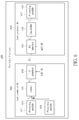
- FIG. 1 is a diagram illustrating multiple semiconductor dies assembled in the same package according to a first embodiment of the present invention.
- a wafer-level package 100 has two semiconductor dies 102 and 104 assembled therein.
- the semiconductor dies 102 and 104 are homogeneous dies (i.e., identical dies) or heterogeneous dies (i.e., distinct dies), and/or the semiconductor dies 102 and 104 are assembled in the wafer-level package 100 to perform a network switch function.
- this is for illustrative purposes only, and is not meant to be a limitation of the present invention. Any wafer-level package using the proposed signal count reduction technique falls within the scope of the present invention.
- the semiconductor die 102 has a processing circuit 112, a multiplexer (MUX) 114, and a transmit (TX) interface 116.
- the processing circuit 112 has a single processing module (e.g., a master engine) 113 arranged to generate a plurality of signal outputs (e.g., A and B) at an engine clock eng_ck.
- a time domain multiplexing technique is employed for signal count reduction between semiconductor dies 102 and 104.
- the multiplexer 114 is arranged to multiplex the signal outputs (e.g., A and B) into a multiplexed signal (e.g., C).
- the transmit interface 116 is arranged to transmit the multiplexed signal (e.g., C) to the semiconductor die 104 at an interface clock info_ck, where the clock frequency F2 of the interface clock info_ck is higher than the clock frequency F1 of the engine clock eng_ck.
- FIG. 2 is a timing diagram illustrating a time domain multiplexing technique employed for signal count reduction between semiconductor dies 102 and 104 according to an embodiment of the present invention.
- the signal outputs A and B are simultaneously sampled at a rising edge of the engine clock eng_ck, where a sample value of the signal output A is '0', and a sample value of the signal output B is '0'.
- the sample values of the signal outputs A and B are sequentially transmitted during two consecutive clock periods P1 and P2 of the interface clock info_ck.
- the signal outputs A and B are simultaneously sampled at a rising edge of the engine clock eng_ck, where a sample value of the signal output A is '1', and a sample value of the signal output B is '0'.
- the sample values of the signal outputs A and B are sequentially transmitted during two consecutive clock periods P3 and P4 of the interface clock info_ck. Since the following time domain multiplexing technique can be deduced by analogy, further description is omitted here for brevity.
- the semiconductor die 104 has a processing circuit 122, a demultiplexer (DEMUX) 124, and a receive (RX) interface 126.
- the receive interface 126 is arranged to receive the multiplexed signal C (which is generated from signal multiplexing performed on the semiconductor die 102) according to the interface clock info_ck.
- the demultiplexer 124 at the RX side is arranged to perform an inverse operation of the signal multiplexing performed by the multiplexer 114 at the TX side. That is, the demultiplexer 124 is arranged to demultiplex a multiplexed signal (e.g., C) into a plurality of signal inputs (e.g., A' and B').
- the signal inputs (e.g., A' and B') correspondingly recovered at the RX side should be identical to the signal outputs (e.g., A and B) correspondingly generated at the TX side and keep relative timing relationship.
- the processing circuit 122 has a single processing module (e.g., a slave engine) 123 arranged to receive and process the signal inputs A' and B' at the engine clock eng_ck. Since a person skilled in the art can readily understand details of signal demultiplexing after reading paragraphs directed to signal multiplexing illustrated in FIG. 2 , further description is omitted here for brevity.
- FIG. 3 is a diagram illustrating multiple semiconductor dies assembled in the same package according to a second embodiment of the present invention.
- a wafer-level package 300 has two semiconductor dies 302 and 304 assembled therein.
- the wafer-level package 300 may be an integrated fan-out (InFO) package, and/or the semiconductor dies 302 and 304 are arranged to perform a network switch function.
- InFO integrated fan-out
- this is for illustrative purposes only, and is not meant to be a limitation of the present invention. Any wafer-level package using the proposed signal count reduction technique falls within the scope of the present invention.
- the semiconductor die 302 has a processing circuit 31 2, a multiplexer (MUX) 316, and a transmit (TX) interface 31 8.
- the processing circuit 312 has multiple processing modules (e.g., master engines) 31 3 and 314 operating at the engine clock eng_ck and arranged to generate a plurality of signal outputs A and B, respectively.
- a function guaranteed time domain multiplexing technique is employed for signal count reduction between semiconductor dies 302 and 304.
- the processing modules 313 and 314 are arranged to generate the signal outputs A and B, correspondingly (e.g., alternately).
- the processing modules e.g., 313 and 314.
- the rest of the processing modules e.g., 313 and 314) are operated in an execution state; in addition, the processing modules (e.g., 313 and 314) alternately enter the communication state in a pre-defined order.
- the processing module 313 is operated in the communication state
- the processing module 314 is operated in the execution state; and when the processing module 313 is operated in the execution state, the processing module 314 is operated in the communication state.
- the processing module 313 is operated in the communication state to generate the signal output A to the multiplexer 316
- the processing module 314 is operated in the execution state without generating the signal output B to the multiplexer 31 6; and while the processing module 313 is operated in the execution state without generating the signal output A to the multiplexer 316, the processing module 314 is operated in the communication state to generate the signal output B to the multiplexer 316.
- the multiplexer 316 is arranged to multiplex the signal outputs (e.g., A and B) into a multiplexed signal (e.g., C).
- the transmit interface 318 is arranged to transmit the multiplexed signal (e.g., C) to the semiconductor die 304 at an interface clock info_ck.
- the clock frequency F2 of the interface clock info_ck may be equal to or different from the clock frequency F1 of the engine clock eng_ck, depending upon actual design considerations.
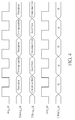
- FIG. 4 is a timing diagram illustrating a function guaranteed time domain multiplexing technique employed for signal count reduction between semiconductor dies 302 and 304 of FIG. 3 according to an embodiment of the present invention.
- the engine clock eng_ck and the interface clock info_ck have the same clock frequency.
- a first module X e.g., processing module 313 enters the execution state and the communication state, alternately.
- a second module Y e.g., processing module 314) enters the communication state and the execution state, alternately.
- the first module X and the second module Y do not operate in the communication state during the same engine clock period.
- the multiplexed signal C carries the signal output B and the signal output A, alternately.
- the semiconductor die 304 has a processing circuit 322, a demultiplexer (DEMUX) 326, and a receive (RX) interface 328.
- the receive interface 328 is arranged to receive the multiplexed signal C (which is generated from signal multiplexing performed on the semiconductor die 302) according to the interface clock info_ck.
- the demultiplexer 326 at the RX side is arranged to perform an inverse operation of the signal multiplexing performed by the multiplexer 316 at the TX side. That is, the demultiplexer 326 is arranged to demultiplex a multiplexed signal (e.g., C) into a plurality of signal inputs (e.g., A' and B').
- the signal inputs (e.g., A' and B') correspondingly recovered at the RX side should be identical to the signal outputs (e.g., A and B) correspondingly generated at the TX side and keep relative timing relationship.
- the processing circuit 322 has multiple processing modules (e.g., slave engines) 323 and 324 arranged to receive and process the signal inputs A' and B' at the engine clock eng_ck.
- the demultiplexer 326 correspondingly (e.g., alternately) generates the signal inputs (e.g., A' and B') recovered at the RX side to the counterpart RX-side processing modules (e.g., 323 and 324) in the same pre-defined order. Since a person skilled in the art can readily understand details of signal demultiplexing after reading paragraphs directed to signal multiplexing illustrated in FIG. 4 , further description is omitted here for brevity.
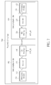
- FIG. 5 is a diagram illustrating multiple semiconductor dies assembled in the same package according to a third embodiment of the present invention.
- a wafer-level package 500 has two semiconductor dies 502 and 504 assembled therein.
- the wafer-level package 500 is an integrated fan-out (InFO) package, and/or the semiconductor dies 502 and 504 are arranged to perform a network switch function.
- InFO integrated fan-out
- this is for illustrative purposes only, and is not meant to be a limitation of the present invention. Any wafer-level package using the proposed signal count reduction technique falls within the scope of the present invention.
- the semiconductor die 502 has a processing circuit 512, an arbiter 516, and a transmit (TX) interface 518.
- the processing circuit 512 has multiple processing modules (e.g., master engines) 51 3 and 514 arranged to generate a plurality of signal outputs A and B, respectively.
- the processing modules 513 and 514 can be active at the same time and thus can issue transmission requests at the same time.
- the arbiter 516 is arranged to perform arbitration upon transmission requests (e.g., write requests) issued from the processing modules 513 and 514 and generate an arbitrated signal C according to one of the signal outputs A and B.
- the arbiter 51 6 when the processing module 51 3 is granted to access the transmission bus between semiconductor dies 502 and 504, the arbiter 51 6 generates the signal output A to the TX interface 51 8, and instructs the processing module 514 to wait for availability of the transmission bus between semiconductor dies 502 and 504.
- the arbiter 516 when the processing module 514 is granted to access the transmission bus between semiconductor dies 502 and 504, the arbiter 516 generates the signal output B to the TX interface 518, and instructs the processing module 513 to wait for availability of the transmission bus between semiconductor dies 502 and 504.
- the arbiter 516 performs flow control upon the processing modules 513 and 514, such that only one of the processing modules 513 and 514 can be allowed to send its signal output through the arbiter 516 at a time.
- the arbiter 516 is further arranged to generate identification information ID that indicates which of the processing modules 513 and 514 issues a transmission request granted by the arbiter 516. For example, when the processing module 513 is granted to access the transmission bus between semiconductor dies 502 and 504, the arbiter 516 sets and outputs the identification information ID of the processing module 513. For another example, when the processing module 514 is granted to access the transmission bus between semiconductor dies 502 and 504, the arbiter 516 sets and outputs the identification information ID of the processing module 514. After the arbitrated signal C and the associated identification information ID are generated from the arbiter 516, the transmit interface 518 is arranged to transmit the arbitrated signal C and the associated identification information ID to the semiconductor die 504 at an interface clock info_ck.
- the semiconductor die 504 has a processing circuit 522, a dispatcher 526, and a receive (RX) interface 528.
- the receive interface 528 is arranged to receive the arbitrated signal C (which is generated from transmission arbitration performed on the semiconductor die 502) and the associated identification information ID according to the interface clock info_ck.
- the processing circuit 522 has multiple processing modules 523 and 524 for processing messages generated from the multiple processing modules 513 and 514 respectively.
- the processing modules 523 at the RX side is arranged to receive a signal input A' derived from the signal output A generated from the processing module 513 at the TX side
- the processing modules 524 at the RX side is arranged to receive a signal input B' derived from the signal output B generated from the processing module 514 at the TX side.
- the signal input A' recovered at the RX side should be identical to the signal input A generated at the TX side
- the signal input B' recovered at the RX side should be identical to the signal input B generated at the TX side.
- the dispatcher 526 at the RX side is arranged to dispatch the arbitrated signal C to one of the processing modules 523 and 524. More specifically, the dispatcher 526 refers to the identification information ID to determine a destination processing module among the processing modules 523 and 524, and dispatches the arbitrated signal C as a signal input to the destination processing module.
- the identification information ID may be an additional signal for a transmission bus between the semiconductor dies 502 and 504.
- the identification information ID is already supported by an adopted bus protocol.
- the master source e.g., master engine side
- AWID write address ID
- ARID read address ID
- FIG. 6 is a diagram illustrating multiple semiconductor dies assembled in the same package according to a fourth embodiment of the present invention.
- a wafer-level package 600 has two semiconductor dies 602 and 604 assembled therein.
- the wafer-level package 600 is an integrated fan-out (InFO) package, and/or the semiconductor dies 602 and 604 are arranged to perform a network switch function.
- InFO integrated fan-out
- this is for illustrative purposes only, and is not meant to be a limitation of the present invention. Any wafer-level package using the proposed signal count reduction technique falls within the scope of the present invention.
- the semiconductor die 604 has a processing circuit 622 (which includes a single processing module 623), a dispatcher 626, and a receive (RX) interface 628.
- the processing module 623 can be seen as one destination processing module located at the RX side for processing messages generated from more than one processing module at the TX side.
- the semiconductor die 602 has a processing circuit 612 (which has multiple processing modules 61 3 and 614), an arbiter 61 6, and a transmit (TX) interface 618.
- the major difference between the semiconductor dies 502 and 602 is that the arbiter 616 performs arbitration upon transmission requests issued from processing modules 613 and 614 to generate an arbitrated signal C to the transmit interface 618 without associated identification information ID.
- the reason is that the processing module 622 doesn't need to know the transmission request is generated from which one of the processing module 613 and 614.
- the signal outputs A and B generated from the processing modules 613 and 614 are all sent to the same destination processing module (i.e., processing module 623), there is no need to generate the identification information to indicate a source of the arbitrated signal C, and the dispatcher 626 dispatches the arbitrated signal C to the processing module 623 only.
- FIG. 7 is a diagram illustrating multiple semiconductor dies assembled in the same package according to a fifth embodiment of the present invention.
- a wafer-level package 700 has two semiconductor dies 702 and 704 assembled therein.
- the wafer-level package 700 is an integrated fan-out (InFO) package, and/or the semiconductor dies 702 and 704 are arranged to perform a network switch function.
- InFO integrated fan-out
- this is for illustrative purposes only, and is not meant to be a limitation of the present invention. Any wafer-level package using the proposed signal count reduction technique falls within the scope of the present invention.
- the semiconductor die 702 has a processing circuit 712, an encoder 714, and a transmit (TX) interface 71 6.
- the processing circuit 712 has one processing module (e.g., master engine) 713 arranged to generate a first signal output A in a first signal waveform.
- the first signal output A is a less changed signal that has a logic high level lasting for at least two clock cycles or has a logic low level lasting for at least two clock cycles.
- the less changed signal is a status signal such as an interrupt signal.
- this is for illustrative purposes only, and is not meant to be a limitation of the present invention. Therefore, the first signal output A seldom toggles due to its inherent characteristics.
- a toggle information delivery technique is employed for signal update frequency reduction between semiconductor dies 702 and 704.
- the encoder 714 is arranged to perform toggle information encoding for encoding the first signal output A to generate a second signal output B in a second signal waveform, wherein the second signal waveform is different from the first signal waveform.
- the encoder 714 generates the second signal output B according to toggle information of the first signal output A, such that the toggle information is sent to the semiconductor die 704 via the transmit interface 716.
- the semiconductor die 704 has a processing circuit 722, a decoder 724, and a receive (RX) interface 726.
- the receive interface 726 is arranged to receive a second signal input B' in a second signal waveform from the semiconductor die 702.
- the second signal input B' received at the RX side is identical to the second signal output B generated at the TX side.
- the decoder 724 at the RX side is arranged to perform an inverse operation of toggle information encoding performed by the encoder 714 at the TX side. That is, the decoder 724 is arranged to decode the second signal input B' to generate a first signal input A' in a first signal waveform different from the second signal waveform.
- the status signal (e.g., interrupt signal) is restored by toggle information delivered over the transmission bus (e.g., InFO bus) between semiconductor dies 702 and 704.
- the first signal input A' recovered at the RX side is identical to the first signal output A generated at the TX side.
- the processing module 723 receives the first signal input A' and operates in response to the received first signal input A'.
- FIG. 8 is a timing diagram illustrating a toggle information delivery technique employed for signal update frequency reduction between semiconductor dies 702 and 704 according to an embodiment of the present invention.
- One signal output generated from a TX-side module X (e.g., processing module 71 3) toggles at time points T1 and T4. Only the toggle information Togglex of the signal output generated from the TX-side module X is transmitted. That is, when a signal toggle event (e.g., 1-to-0 signal level transition, or 0-to-1 signal level transition) occurs, the associated toggle information Toggle x is transmitted. However, when the signal level remains unchanged, no signal transmission is needed to carry the constant signal level.
- a signal toggle event e.g., 1-to-0 signal level transition, or 0-to-1 signal level transition
- the bandwidth occupation of the transmission bus (e.g., InFO bus) between semiconductor dies 702 and 704 can be reduced due to that fact that only the toggle information Togglex of the signal output generated from the TX-side module X is transmitted.
- the signal update frequency can be reduced, the available bandwidth of the transmission bus (e.g., InFO bus) between semiconductor dies 702 and 704 can be increased correspondingly.
- the toggle information Toggle x' received at the RX side is decoded to restore a signal input that is transmitted to an RX-side module X' (e.g., processing module 723).
- FIG. 9 is a diagram illustrating an example of delivering a 32-bit interrupt signal from one semiconductor die to another semiconductor die.
- the interrupt signal IRQ ⁇ 31:0> generated by one semiconductor die at the TX side is a status signal that seldom toggles.
- the aforementioned toggle information delivery technique can be used to carry the toggle information via a transmission bus (e.g., InFO bus) between two semiconductor dies assembled in the same wafer-level package (e.g., InFO package).
- a transmission bus e.g., InFO bus
- ToggleID 5'b1_0000.
- ToggleID 5'b0_0001.
- the toggle information (i.e., ToggleID) is transmitted from the semiconductor die at the TX side to another semiconductor die at the RX side.
- the semiconductor die at the RX side can refer to the received ToggleID to restore an interrupt signal IRQ' ⁇ 31:0>.
- toggle information delivery technique employed by the chip design shown in FIG. 7 may be incorporated into the aforementioned chip designs shown in FIGs. 1 , 3 , 5 and 6 . That is, a wafer-level package may be configured to employ the proposed signal count reduction technique as well as the proposed ideas of signal update frequency reduction. This also falls within the scope of the present invention.
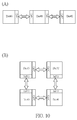
- FIG. 10 is a diagram illustrating different wafer-level package designs according to an embodiment of the present invention.
- the sub-diagram (A) of FIG. 10 shows a wafer-level package (e.g., InFO package) having three semiconductor dies Die#0, Die#1, Die#2 assembled therein.
- the sub-diagram (B) of FIG. 10 shows a wafer-level package (e.g., InFO package) having four semiconductor dies Die#0, Die#1, Die#2, Die#3 assembled therein.
- the proposed signal count reduction technique is employed by the wafer-level packages shown in FIG. 10
- the reduction of die area can be achieved (e.g., required side length for configuring signals between dies can be reduced based on the fewer signal count).
- the proposed signal update frequency reduction technique is employed by the wafer-level packages shown in FIG. 10
- the bandwidth utilization can be improved. To put it simply, any wafer-level package with two or more semiconductor dies using proposed signal count reduction technique and/or proposed signal update frequency reduction technique falls within the scope of the present invention.
Landscapes
- Engineering & Computer Science (AREA)
- Theoretical Computer Science (AREA)
- General Engineering & Computer Science (AREA)
- Physics & Mathematics (AREA)
- General Physics & Mathematics (AREA)
- Computer Hardware Design (AREA)
- Semiconductor Integrated Circuits (AREA)
Abstract
Description
- The present invention relates to a signal count reduction technique applied to a wafer-level package having multiple semiconductor dies assembled therein.
- When a chip function of a target chip is achieved using a large-sized die, the fabrication of large-sized dies on a wafer will suffer from low yield and high cost. Given the same die area, the yield of one large die is lower than the yield of multiple small dies. More specifically, assuming that distribution of defects on a wafer is the same, a die yield of one large-sized die fabricated on the wafer is lower than a die yield of multiple small-sized dies which have the same area fabricated on the same wafer. However, splitting one large die into multiple smaller dies may bring some overhead. For example, a large number of signals will be introduced to achieve communications between different small-sized dies. As a result, an extra area will be needed by signal trace routing when more signals are needed to be transmitted between small-sized dies. Consequently, the production cost of using small-sized dies to implement the full function of a large-sized die is increased due to the extra area needed by signal traces routed between small-sized dies. Thus, there is a need for an innovative design which can achieve signal count reduction between dies.
- This in mind, the present invention aims at providing a signal count reduction technique applied to a wafer-level package having multiple semiconductor dies assembled therein.
- This is achieved by wafer-level packages according to
claims 1, 4, 6, 8, 11 and 13. The dependent claims pertain to corresponding further developments and improvements. - As will be seen more clearly from the detailed description following below, the claimed semiconductor die assembled in a wafer-level package includes a processing circuit, a multiplexer, and a transmit interface. The processing circuit is arranged to generate a plurality of signal outputs. The multiplexer is arranged to multiplex the signal outputs into a multiplexed signal. The transmit interface is arranged to transmit the multiplexed signal to another semiconductor die assembled in the wafer-level package.
- Another claimed semiconductor die assembled in a wafer-level package includes a processing circuit, an arbiter, and a transmit interface. The processing circuit has a plurality of processing modules arranged to generate a plurality of signal outputs, respectively. The arbiter is arranged to perform arbitration upon transmission requests issued from the processing modules and generate an arbitrated signal according to one of the signal outputs. The transmit interface is arranged to transmit the arbitrated signal to another semiconductor die assembled in the wafer-level package.
- Another claimed semiconductor die assembled in a wafer-level package includes a processing circuit, an encoder, and a transmit interface. The processing circuit is arranged to generate a first signal output in a first signal waveform. The encoder is arranged to encode the first signal output to generate a second signal output in a second signal waveform, wherein the second signal waveform is different from the first signal waveform. The transmit interface is arranged to transmit the second signal output to another semiconductor die assembled in the wafer-level package.
- Another claimed semiconductor die assembled in a wafer-level package includes a receive interface, a demultiplexer, and a processing circuit. The receive interface is arranged to receive a multiplexed signal generated from another semiconductor die assembled in the wafer-level package. The demultiplexer is arranged to demultiplex the multiplexed signal into a plurality of signal inputs. The processing circuit is arranged to receive the signal inputs from the demultiplexer.
- Another claimed semiconductor die assembled in a wafer-level package includes a receive interface, a processing circuit, and a dispatcher. The receive interface is arranged to receive an arbitrated signal generated from another semiconductor die assembled in the wafer-level package. The processing circuit has at least one processing module. The dispatcher is arranged to dispatch the arbitrated signal to the at least one processing module.
- Another claimed semiconductor die assembled in a wafer-level package includes a receive interface, a decoder, and a processing circuit. The receive interface is arranged to receive a second signal output in a second signal waveform from another semiconductor die assembled in the wafer-level package. The decoder is arranged to decode the second signal input to generate a first signal input in a first signal waveform, wherein the second signal waveform is different from the first signal waveform. The processing circuit is arranged to receive the first signal input.
- In the following, the invention is further illustrated by way of example, taking reference to the accompanying drawings. Thereof
-
FIG. 1 is a diagram illustrating multiple semiconductor dies assembled in the same package according to a first embodiment of the present invention, -
FIG. 2 is a timing diagram illustrating a time domain multiplexing technique employed for signal count reduction between semiconductor dies according to an embodiment of the present invention, -
FIG. 3 is a diagram illustrating multiple semiconductor dies assembled in the same package according to a second embodiment of the present invention, -
FIG. 4 is a timing diagram illustrating a function guaranteed time domain multiplexing technique employed for signal count reduction between semiconductor dies according to an embodiment of the present invention, -
FIG. 5 is a diagram illustrating multiple semiconductor dies assembled in the same package according to a third embodiment of the present invention, -
FIG. 6 is a diagram illustrating multiple semiconductor dies assembled in the same package according to a fourth embodiment of the present invention, -
FIG. 7 is a diagram illustrating multiple semiconductor dies assembled in the same package according to a fifth embodiment of the present invention, -
FIG. 8 is a timing diagram illustrating a toggle information delivery technique employed for signal update frequency reduction between semiconductor dies according to an embodiment of the present invention, -
FIG. 9 is a diagram illustrating an example of delivering a 32-bit interrupt signal from one semiconductor die to another semiconductor die, and -
FIG. 10 is a diagram illustrating different wafer-level package designs according to an embodiment of the present invention. - Certain terms are used throughout the following description and claims, which refer to particular components. As one skilled in the art will appreciate, electronic equipment manufacturers may refer to a component by different names. This document does not intend to distinguish between components that differ in name but not in function. In the following description and in the claims, the terms "include" and "comprise" are used in an open-ended fashion, and thus should be interpreted to mean "include, but not limited to ...". Also, the term "couple" is intended to mean either an indirect or direct electrical connection. Accordingly, if one device is coupled to another device, that connection may be through a direct electrical connection, or through an indirect electrical connection via other devices and connections.
- Wafer-level packaging is the technology of packaging semiconductor dies, which is different from a typical packaging method of slicing a wafer into individual semiconductor dies and then packaging the individual semiconductor dies. The wafer-level package mentioned above is therefore fabricated based on wafer-level process. That is, multiple semiconductor dies (e.g., homogeneous dies or heterogeneous dies) assembled in the same wafer-level package and connection paths/transmission buses/communication channels and so on routed between the semiconductor dies are fabricated with wafer-level process. Hence, connection paths, communication buses, or communication channels could be implemented by metal layer (such as RDL metal layer, Re-Distribution Layer, a metal layer on a die that makes the I/O pads of an integrated circuit available in other locations) rather than bonding wire of typical package.
- The wafer-level package may be an integrated fan-out (InFO) package or a chip on wafer on substrate (CoWoS) package. Take InFO packages as examples for the following wafer-level packages, but not for a limitation. The wafer-level package used for the proposed ideas may be an InFO package or a CoWoS package, "InFO package" and "CoWoS package" may be interchangeable.
-
FIG. 1 is a diagram illustrating multiple semiconductor dies assembled in the same package according to a first embodiment of the present invention. In this embodiment, a wafer-level package 100 has two semiconductor dies 102 and 104 assembled therein. The semiconductor dies 102 and 104 are homogeneous dies (i.e., identical dies) or heterogeneous dies (i.e., distinct dies), and/or the semiconductor dies 102 and 104 are assembled in the wafer-level package 100 to perform a network switch function. However, this is for illustrative purposes only, and is not meant to be a limitation of the present invention. Any wafer-level package using the proposed signal count reduction technique falls within the scope of the present invention. - The semiconductor die 102 has a
processing circuit 112, a multiplexer (MUX) 114, and a transmit (TX)interface 116. In this embodiment, theprocessing circuit 112 has a single processing module (e.g., a master engine) 113 arranged to generate a plurality of signal outputs (e.g., A and B) at an engine clock eng_ck. In this embodiment, a time domain multiplexing technique is employed for signal count reduction between semiconductor dies 102 and 104. Hence, themultiplexer 114 is arranged to multiplex the signal outputs (e.g., A and B) into a multiplexed signal (e.g., C). The transmitinterface 116 is arranged to transmit the multiplexed signal (e.g., C) to the semiconductor die 104 at an interface clock info_ck, where the clock frequency F2 of the interface clock info_ck is higher than the clock frequency F1 of the engine clock eng_ck. - The engine clock eng_ck can run at any clock frequency F1, and the data compression rate depends on the ratio between clock frequencies F1 and F2 of in-phase (e.g., multiple frequency)/synchronous (e.g., same frequency) engine clock eng_ck and interface clock info_ck. For example, if the clock frequency ratio of engine clock eng_ck and interface clock info_ck is 2:3 (i.e., F1 :F2=2:3), consecutive 2T messages transmitted on the basis of the engine clock eng_ck can be carried on consecutive 3T messages transmitted on the basis of the interface clock info_ck, where the signal count can be reduced to 2/3.
-
FIG. 2 is a timing diagram illustrating a time domain multiplexing technique employed for signal count reduction between semiconductor dies 102 and 104 according to an embodiment of the present invention. Assume that the clock frequency ratio of engine clock eng_ck and interface clock info_ck is 1:2 (i.e., F1:F2=1:2). Hence, there are two interface clock periods within one engine clock period. At the time point T1, the signal outputs A and B are simultaneously sampled at a rising edge of the engine clock eng_ck, where a sample value of the signal output A is '0', and a sample value of the signal output B is '0'. The sample values of the signal outputs A and B are sequentially transmitted during two consecutive clock periods P1 and P2 of the interface clock info_ck. Similarly, at the time point T2, the signal outputs A and B are simultaneously sampled at a rising edge of the engine clock eng_ck, where a sample value of the signal output A is '1', and a sample value of the signal output B is '0'. The sample values of the signal outputs A and B are sequentially transmitted during two consecutive clock periods P3 and P4 of the interface clock info_ck. Since the following time domain multiplexing technique can be deduced by analogy, further description is omitted here for brevity. - With regard to the semiconductor die 104, it has a
processing circuit 122, a demultiplexer (DEMUX) 124, and a receive (RX)interface 126. The receiveinterface 126 is arranged to receive the multiplexed signal C (which is generated from signal multiplexing performed on the semiconductor die 102) according to the interface clock info_ck. Thedemultiplexer 124 at the RX side is arranged to perform an inverse operation of the signal multiplexing performed by themultiplexer 114 at the TX side. That is, thedemultiplexer 124 is arranged to demultiplex a multiplexed signal (e.g., C) into a plurality of signal inputs (e.g., A' and B'). - Ideally, the signal inputs (e.g., A' and B') correspondingly recovered at the RX side should be identical to the signal outputs (e.g., A and B) correspondingly generated at the TX side and keep relative timing relationship. The
processing circuit 122 has a single processing module (e.g., a slave engine) 123 arranged to receive and process the signal inputs A' and B' at the engine clock eng_ck. Since a person skilled in the art can readily understand details of signal demultiplexing after reading paragraphs directed to signal multiplexing illustrated inFIG. 2 , further description is omitted here for brevity. -
FIG. 3 is a diagram illustrating multiple semiconductor dies assembled in the same package according to a second embodiment of the present invention. In this embodiment, a wafer-level package 300 has two semiconductor dies 302 and 304 assembled therein. For example, the wafer-level package 300 may be an integrated fan-out (InFO) package, and/or the semiconductor dies 302 and 304 are arranged to perform a network switch function. However, this is for illustrative purposes only, and is not meant to be a limitation of the present invention. Any wafer-level package using the proposed signal count reduction technique falls within the scope of the present invention. - In this embodiment, the semiconductor die 302 has a
processing circuit 31 2, a multiplexer (MUX) 316, and a transmit (TX)interface 31 8. Theprocessing circuit 312 has multiple processing modules (e.g., master engines) 31 3 and 314 operating at the engine clock eng_ck and arranged to generate a plurality of signal outputs A and B, respectively. In addition, a function guaranteed time domain multiplexing technique is employed for signal count reduction between semiconductor dies 302 and 304. Hence, theprocessing modules - For example, when one of the processing modules (e.g., 313 and 314) is operated in a communication state to generate a corresponding signal output, the rest of the processing modules (e.g., 313 and 314) are operated in an execution state; in addition, the processing modules (e.g., 313 and 314) alternately enter the communication state in a pre-defined order. Concerning the embodiment shown in
FIG. 3 , when theprocessing module 313 is operated in the communication state, theprocessing module 314 is operated in the execution state; and when theprocessing module 313 is operated in the execution state, theprocessing module 314 is operated in the communication state. Therefore, while theprocessing module 313 is operated in the communication state to generate the signal output A to themultiplexer 316, theprocessing module 314 is operated in the execution state without generating the signal output B to themultiplexer 31 6; and while theprocessing module 313 is operated in the execution state without generating the signal output A to themultiplexer 316, theprocessing module 314 is operated in the communication state to generate the signal output B to themultiplexer 316. - The
multiplexer 316 is arranged to multiplex the signal outputs (e.g., A and B) into a multiplexed signal (e.g., C). The transmitinterface 318 is arranged to transmit the multiplexed signal (e.g., C) to the semiconductor die 304 at an interface clock info_ck. It should be noted that the clock frequency F2 of the interface clock info_ck may be equal to or different from the clock frequency F1 of the engine clock eng_ck, depending upon actual design considerations. -
FIG. 4 is a timing diagram illustrating a function guaranteed time domain multiplexing technique employed for signal count reduction between semiconductor dies 302 and 304 ofFIG. 3 according to an embodiment of the present invention. Assume that the engine clock eng_ck and the interface clock info_ck have the same clock frequency. A first module X (e.g., processing module 313) enters the execution state and the communication state, alternately. A second module Y (e.g., processing module 314) enters the communication state and the execution state, alternately. Hence, the first module X and the second module Y do not operate in the communication state during the same engine clock period. In this way, the multiplexed signal C carries the signal output B and the signal output A, alternately. - Concerning the semiconductor die 304, it has a
processing circuit 322, a demultiplexer (DEMUX) 326, and a receive (RX)interface 328. The receiveinterface 328 is arranged to receive the multiplexed signal C (which is generated from signal multiplexing performed on the semiconductor die 302) according to the interface clock info_ck. Thedemultiplexer 326 at the RX side is arranged to perform an inverse operation of the signal multiplexing performed by themultiplexer 316 at the TX side. That is, thedemultiplexer 326 is arranged to demultiplex a multiplexed signal (e.g., C) into a plurality of signal inputs (e.g., A' and B'). - Ideally, the signal inputs (e.g., A' and B') correspondingly recovered at the RX side should be identical to the signal outputs (e.g., A and B) correspondingly generated at the TX side and keep relative timing relationship. The
processing circuit 322 has multiple processing modules (e.g., slave engines) 323 and 324 arranged to receive and process the signal inputs A' and B' at the engine clock eng_ck. Since the TX-side processing modules (e.g., 313 and 314) alternately enter the communication state in a pre-defined order, thedemultiplexer 326 correspondingly (e.g., alternately) generates the signal inputs (e.g., A' and B') recovered at the RX side to the counterpart RX-side processing modules (e.g., 323 and 324) in the same pre-defined order. Since a person skilled in the art can readily understand details of signal demultiplexing after reading paragraphs directed to signal multiplexing illustrated inFIG. 4 , further description is omitted here for brevity. -
FIG. 5 is a diagram illustrating multiple semiconductor dies assembled in the same package according to a third embodiment of the present invention. In this embodiment, a wafer-level package 500 has two semiconductor dies 502 and 504 assembled therein. For example, the wafer-level package 500 is an integrated fan-out (InFO) package, and/or the semiconductor dies 502 and 504 are arranged to perform a network switch function. However, this is for illustrative purposes only, and is not meant to be a limitation of the present invention. Any wafer-level package using the proposed signal count reduction technique falls within the scope of the present invention. - In this embodiment, the semiconductor die 502 has a
processing circuit 512, anarbiter 516, and a transmit (TX)interface 518. Theprocessing circuit 512 has multiple processing modules (e.g., master engines) 51 3 and 514 arranged to generate a plurality of signal outputs A and B, respectively. In this embodiment, theprocessing modules arbiter 516 is arranged to perform arbitration upon transmission requests (e.g., write requests) issued from theprocessing modules - For example, when the processing module 51 3 is granted to access the transmission bus between semiconductor dies 502 and 504, the arbiter 51 6 generates the signal output A to the TX interface 51 8, and instructs the
processing module 514 to wait for availability of the transmission bus between semiconductor dies 502 and 504. For another example, when theprocessing module 514 is granted to access the transmission bus between semiconductor dies 502 and 504, thearbiter 516 generates the signal output B to theTX interface 518, and instructs theprocessing module 513 to wait for availability of the transmission bus between semiconductor dies 502 and 504. To put it simply, thearbiter 516 performs flow control upon theprocessing modules processing modules arbiter 516 at a time. - Moreover, the
arbiter 516 is further arranged to generate identification information ID that indicates which of theprocessing modules arbiter 516. For example, when theprocessing module 513 is granted to access the transmission bus between semiconductor dies 502 and 504, thearbiter 516 sets and outputs the identification information ID of theprocessing module 513. For another example, when theprocessing module 514 is granted to access the transmission bus between semiconductor dies 502 and 504, thearbiter 516 sets and outputs the identification information ID of theprocessing module 514. After the arbitrated signal C and the associated identification information ID are generated from thearbiter 516, the transmitinterface 518 is arranged to transmit the arbitrated signal C and the associated identification information ID to the semiconductor die 504 at an interface clock info_ck. - With regard to the semiconductor die 504, it has a
processing circuit 522, adispatcher 526, and a receive (RX)interface 528. The receiveinterface 528 is arranged to receive the arbitrated signal C (which is generated from transmission arbitration performed on the semiconductor die 502) and the associated identification information ID according to the interface clock info_ck. Theprocessing circuit 522 hasmultiple processing modules multiple processing modules - For example, the
processing modules 523 at the RX side is arranged to receive a signal input A' derived from the signal output A generated from theprocessing module 513 at the TX side, and theprocessing modules 524 at the RX side is arranged to receive a signal input B' derived from the signal output B generated from theprocessing module 514 at the TX side. Ideally, the signal input A' recovered at the RX side should be identical to the signal input A generated at the TX side, and the signal input B' recovered at the RX side should be identical to the signal input B generated at the TX side. - The
dispatcher 526 at the RX side is arranged to dispatch the arbitrated signal C to one of theprocessing modules dispatcher 526 refers to the identification information ID to determine a destination processing module among the processingmodules - In one implementation, the identification information ID may be an additional signal for a transmission bus between the semiconductor dies 502 and 504. However, this is for illustrative purposes only, and is not meant to be a limitation of the present invention. In an alternative design, the identification information ID is already supported by an adopted bus protocol. For example, when an Advanced extensible Interface (AXI) bus protocol is employed, the master source (e.g., master engine side) can be identified by AWID (write address ID)/ARID (read address ID) specified in the AXI bus protocol.
-
FIG. 6 is a diagram illustrating multiple semiconductor dies assembled in the same package according to a fourth embodiment of the present invention. In this embodiment, a wafer-level package 600 has two semiconductor dies 602 and 604 assembled therein. For example, the wafer-level package 600 is an integrated fan-out (InFO) package, and/or the semiconductor dies 602 and 604 are arranged to perform a network switch function. However, this is for illustrative purposes only, and is not meant to be a limitation of the present invention. Any wafer-level package using the proposed signal count reduction technique falls within the scope of the present invention. - The semiconductor die 604 has a processing circuit 622 (which includes a single processing module 623), a
dispatcher 626, and a receive (RX)interface 628. In this embodiment, theprocessing module 623 can be seen as one destination processing module located at the RX side for processing messages generated from more than one processing module at the TX side. - Like the semiconductor die 502 shown in
FIG. 5 , the semiconductor die 602 has a processing circuit 612 (which has multiple processing modules 61 3 and 614), an arbiter 61 6, and a transmit (TX)interface 618. The major difference between the semiconductor dies 502 and 602 is that thearbiter 616 performs arbitration upon transmission requests issued from processingmodules interface 618 without associated identification information ID. The reason is that theprocessing module 622 doesn't need to know the transmission request is generated from which one of theprocessing module processing modules dispatcher 626 dispatches the arbitrated signal C to theprocessing module 623 only. -
FIG. 7 is a diagram illustrating multiple semiconductor dies assembled in the same package according to a fifth embodiment of the present invention. In this embodiment, a wafer-level package 700 has two semiconductor dies 702 and 704 assembled therein. For example, the wafer-level package 700 is an integrated fan-out (InFO) package, and/or the semiconductor dies 702 and 704 are arranged to perform a network switch function. However, this is for illustrative purposes only, and is not meant to be a limitation of the present invention. Any wafer-level package using the proposed signal count reduction technique falls within the scope of the present invention. - The semiconductor die 702 has a
processing circuit 712, anencoder 714, and a transmit (TX) interface 71 6. Theprocessing circuit 712 has one processing module (e.g., master engine) 713 arranged to generate a first signal output A in a first signal waveform. For example, the first signal output A is a less changed signal that has a logic high level lasting for at least two clock cycles or has a logic low level lasting for at least two clock cycles. In the following, it is assumed that the less changed signal is a status signal such as an interrupt signal. However, this is for illustrative purposes only, and is not meant to be a limitation of the present invention. Therefore, the first signal output A seldom toggles due to its inherent characteristics. In this embodiment, a toggle information delivery technique is employed for signal update frequency reduction between semiconductor dies 702 and 704. Theencoder 714 is arranged to perform toggle information encoding for encoding the first signal output A to generate a second signal output B in a second signal waveform, wherein the second signal waveform is different from the first signal waveform. For example, theencoder 714 generates the second signal output B according to toggle information of the first signal output A, such that the toggle information is sent to the semiconductor die 704 via the transmitinterface 716. - With regard to the semiconductor die 704, it has a
processing circuit 722, adecoder 724, and a receive (RX)interface 726. The receiveinterface 726 is arranged to receive a second signal input B' in a second signal waveform from the semiconductor die 702. Ideally, the second signal input B' received at the RX side is identical to the second signal output B generated at the TX side. Thedecoder 724 at the RX side is arranged to perform an inverse operation of toggle information encoding performed by theencoder 714 at the TX side. That is, thedecoder 724 is arranged to decode the second signal input B' to generate a first signal input A' in a first signal waveform different from the second signal waveform. - For example, the status signal (e.g., interrupt signal) is restored by toggle information delivered over the transmission bus (e.g., InFO bus) between semiconductor dies 702 and 704. Ideally, the first signal input A' recovered at the RX side is identical to the first signal output A generated at the TX side. After the first signal input A' is recovered by the
decoder 724, theprocessing module 723 receives the first signal input A' and operates in response to the received first signal input A'. -
FIG. 8 is a timing diagram illustrating a toggle information delivery technique employed for signal update frequency reduction between semiconductor dies 702 and 704 according to an embodiment of the present invention. One signal output generated from a TX-side module X (e.g., processing module 71 3) toggles at time points T1 and T4. Only the toggle information Togglex of the signal output generated from the TX-side module X is transmitted. That is, when a signal toggle event (e.g., 1-to-0 signal level transition, or 0-to-1 signal level transition) occurs, the associated toggle information Togglex is transmitted. However, when the signal level remains unchanged, no signal transmission is needed to carry the constant signal level. In this way, the bandwidth occupation of the transmission bus (e.g., InFO bus) between semiconductor dies 702 and 704 can be reduced due to that fact that only the toggle information Togglex of the signal output generated from the TX-side module X is transmitted. Besides, since the signal update frequency can be reduced, the available bandwidth of the transmission bus (e.g., InFO bus) between semiconductor dies 702 and 704 can be increased correspondingly. Further, the toggle information Togglex' received at the RX side is decoded to restore a signal input that is transmitted to an RX-side module X' (e.g., processing module 723). -
FIG. 9 is a diagram illustrating an example of delivering a 32-bit interrupt signal from one semiconductor die to another semiconductor die. The interrupt signal IRQ<31:0> generated by one semiconductor die at the TX side is a status signal that seldom toggles. The aforementioned toggle information delivery technique can be used to carry the toggle information via a transmission bus (e.g., InFO bus) between two semiconductor dies assembled in the same wafer-level package (e.g., InFO package). When the MSB (most significant bit) interrupt toggles, ToggleID = 5'b1_0000. When the LSB (least significant bit) interrupt toggles, ToggleID = 5'b0_0001. In addition, when the interrupt signal IRQ<31:0> has 2 bits changed, a two-phase ToggleID change is generated correspondingly as illustrated by "5'b0_0001" and "5'b1_0000". The toggle information (i.e., ToggleID) is transmitted from the semiconductor die at the TX side to another semiconductor die at the RX side. The semiconductor die at the RX side can refer to the received ToggleID to restore an interrupt signal IRQ'<31:0>. - It should be noted that the toggle information delivery technique employed by the chip design shown in
FIG. 7 may be incorporated into the aforementioned chip designs shown inFIGs. 1 ,3 ,5 and6 . That is, a wafer-level package may be configured to employ the proposed signal count reduction technique as well as the proposed ideas of signal update frequency reduction. This also falls within the scope of the present invention. - In above exemplary embodiments, the wafer-level package is shown having two semiconductor dies using proposed signal count reduction technique and/or proposed signal update frequency reduction technique. However, these are for illustrative purposes only, and are not meant to be limitations of the present invention.
FIG. 10 is a diagram illustrating different wafer-level package designs according to an embodiment of the present invention. The sub-diagram (A) ofFIG. 10 shows a wafer-level package (e.g., InFO package) having three semiconductor diesDie# 0,Die# 1,Die# 2 assembled therein. The sub-diagram (B) ofFIG. 10 shows a wafer-level package (e.g., InFO package) having four semiconductor diesDie# 0,Die# 1,Die# 2,Die# 3 assembled therein. When the proposed signal count reduction technique is employed by the wafer-level packages shown inFIG. 10 , the reduction of die area can be achieved (e.g., required side length for configuring signals between dies can be reduced based on the fewer signal count). When the proposed signal update frequency reduction technique is employed by the wafer-level packages shown inFIG. 10 , the bandwidth utilization can be improved. To put it simply, any wafer-level package with two or more semiconductor dies using proposed signal count reduction technique and/or proposed signal update frequency reduction technique falls within the scope of the present invention.
Claims (15)
- A semiconductor die (102, 302) assembled in a wafer-level package (100, 300), comprising:a processing circuit (112, 312), arranged to generate a plurality of signal outputs;a multiplexer (114, 31 6), arranged to multiple the signal outputs into a multiplexed signal; anda transmit interface (116, 318), arranged to transmit the multiplexed signal to another semiconductor die (104, 304) assembled in the wafer-level package (100, 300).
- The semiconductor die (102) of claim 1, wherein the processing circuit (112) comprises:a single processing module (113), arranged to generate all of the signal outputs.
- The semiconductor die (302) of claim 1, wherein the processing circuit (31 2) comprises:a plurality of processing modules (313, 314), arranged to generate the signal outputs, alternately.
- A semiconductor die (502, 602) assembled in a wafer-level package (500, 600), comprising:a processing circuit (51 2, 61 2), comprising:a plurality of processing modules (513, 514, 613, 614), arranged to generate a plurality of signal outputs, respectively;an arbiter (516, 616), arranged to perform arbitration upon transmission requests issued from the processing modules (51 3, 514, 613, 614) and generate an arbitrated signal according to one of the signal outputs; anda transmit interface (518, 618), arranged to transmit the arbitrated signal to another semiconductor die (504, 604) assembled in the wafer-level package (500, 600).
- The semiconductor die (502) of claim 4, wherein the arbiter (516) is further arranged to generate identification information that indicates which of the processing modules (513, 514) issues a transmission request granted by the arbiter (51 6); and the transmit interface (518) is further arranged to transmit the identification information to the another semiconductor die (504).
- A semiconductor die (702) assembled in a wafer-level package (700), comprising:a processing circuit (71 2), arranged to generate a first signal output in a first signal waveform;an encoder (714), arranged to encode the first signal output to generate a second signal output in a second signal waveform, wherein the second signal waveform is different from the first signal waveform; anda transmit interface (716), arranged to transmit the second signal output to another semiconductor die (704) assembled in the wafer-level package (700).
- The semiconductor die (702) of claim 6, wherein the first signal output is a less changed signal that has a logic high level lasting for at least two clock cycles or has a logic low level lasting for at least two clock cycles; and/or wherein the encoder (714) generates the second signal output according to toggle information of the first signal output.
- A semiconductor die (104, 304) assembled in a wafer-level package (100, 300), comprising:a receive interface (126, 328), arranged to receive a multiplexed signal generated from another semiconductor die (102, 302) assembled in the wafer-level package (100, 300);a demultiplexer (124, 326), arranged to demultiplex the multiplexed signal into a plurality of signal inputs; anda processing circuit (1 22, 322), arranged to receive the signal inputs from the demultiplexer (124, 326).
- The semiconductor die (104) of claim 8, wherein the processing circuit (1 22) comprises:a single processing module (123), arranged to receive all of the signal inputs.
- The semiconductor die (304) of claim 8, wherein the processing circuit (322) comprises:a plurality of processing modules (323, 324), arranged to receive the signal inputs, alternately.
- A semiconductor die (504, 604) assembled in a wafer-level package (500, 600), comprising:a receive interface (528, 628), arranged to receive an arbitrated signal generated from another semiconductor die (502, 602) assembled in the wafer-level package (500, 600);a processing circuit (522, 622), comprising:at least one processing module (523, 524, 623); anda dispatcher (526, 626), arranged to dispatch the arbitrated signal to the at least one processing module (523, 524, 623).
- The semiconductor die (504) of claim 11, wherein the processing circuit (522) comprises a plurality of processing modules (523, 524) arranged to receive a plurality of signal inputs, respectively; and the dispatcher (526) is arranged to dispatch the arbitrated signal as a signal input to a destination processing module of the processing modules (523, 524); and/or wherein the receive interface (528) is further arranged to receive identification information that indicates a source of the arbitrated signal, and the dispatcher (526) is further arranged to dispatch the arbitrated signal according to the identification information.
- A semiconductor die (704) assembled in a wafer-level package (700), comprising:a receive interface (704), arranged to receive a second signal input in a second signal waveform from another semiconductor die (702) assembled in the wafer-level package (700);a decoder (724), arranged to decode the second signal input to generate a first signal input in a first signal waveform, wherein the second signal waveform is different from the first signal waveform; anda processing circuit (722), arranged to receive the first signal input.
- The semiconductor die (704) of claim 13, wherein the first signal input is a less changed signal that has a logic high level lasting for at least two clock cycles or has a logic low level lasting for at least two clock cycles; and/or wherein the decoder (724) generates the first signal input according to toggle information of the second signal input.
- The semiconductor die (102, 104, 302, 304, 502, 504, 602, 604, 702, 704) of claim 1, 4, 6, 8, 11 or 13, wherein the wafer-level package (100, 300, 500, 600, 700) is an integrated fan-out package.
Applications Claiming Priority (3)
| Application Number | Priority Date | Filing Date | Title |
|---|---|---|---|
| US201562117086P | 2015-02-17 | 2015-02-17 | |
| US201562198650P | 2015-07-29 | 2015-07-29 | |
| US15/009,819 US10152445B2 (en) | 2015-02-17 | 2016-01-28 | Signal count reduction between semiconductor dies assembled in wafer-level package |
Publications (1)
| Publication Number | Publication Date |
|---|---|
| EP3059681A1 true EP3059681A1 (en) | 2016-08-24 |
Family
ID=55442646
Family Applications (1)
| Application Number | Title | Priority Date | Filing Date |
|---|---|---|---|
| EP16155812.7A Withdrawn EP3059681A1 (en) | 2015-02-17 | 2016-02-16 | Signal count reduction between semiconductor dies assembled in wafer-level package |
Country Status (3)
| Country | Link |
|---|---|
| US (1) | US10152445B2 (en) |
| EP (1) | EP3059681A1 (en) |
| CN (1) | CN105895630A (en) |
Families Citing this family (8)
| Publication number | Priority date | Publication date | Assignee | Title |
|---|---|---|---|---|
| JP7177699B2 (en) * | 2016-09-20 | 2022-11-24 | 株式会社カネカ | glass building materials |
| CN111143252B (en) * | 2019-11-27 | 2022-06-21 | 网络通信与安全紫金山实验室 | Mimicry control port multiplexing method |
| US11487683B2 (en) * | 2020-04-15 | 2022-11-01 | AyDeeKay LLC | Seamlessly integrated microcontroller chip |
| US11742295B2 (en) | 2020-12-28 | 2023-08-29 | Global Unichip Corporation | Interface of integrated circuit die and method for arranging interface thereof |
| US11063596B1 (en) | 2021-01-07 | 2021-07-13 | Global Unichip Corporation | Frame decoding circuit and method for performing frame decoding |
| US11474554B2 (en) | 2021-01-12 | 2022-10-18 | Global Unichip Corporation | Circuit for providing clock to de-serializer in communication physical layer |
| US11336427B1 (en) | 2021-02-25 | 2022-05-17 | Global Unichip Corporation | Circuit of communication interface between two dies and method to manage communication interface |
| CN120179599A (en) * | 2025-05-21 | 2025-06-20 | 北京芯素科技有限公司 | A SerDes interconnection structure and method between bare chips |
Citations (4)
| Publication number | Priority date | Publication date | Assignee | Title |
|---|---|---|---|---|
| EP0866404A2 (en) * | 1997-03-20 | 1998-09-23 | Sun Microsystems, Inc. | Unbalanced multiplexer and arbiter combination |
| US20050083217A1 (en) * | 2003-10-16 | 2005-04-21 | Kim Hong-Beom | Method for transmitting and receiving signals in semiconductor device and semiconductor device thereof |
| US20090103345A1 (en) * | 2007-10-23 | 2009-04-23 | Mclaren Moray | Three-dimensional memory module architectures |
| US20100211336A1 (en) * | 2009-02-19 | 2010-08-19 | Advanced Micro Devices, Inc. | Data processing interface device |
Family Cites Families (21)
| Publication number | Priority date | Publication date | Assignee | Title |
|---|---|---|---|---|
| US4912633A (en) | 1988-10-24 | 1990-03-27 | Ncr Corporation | Hierarchical multiple bus computer architecture |
| JPH08500687A (en) | 1992-08-10 | 1996-01-23 | モノリシック・システム・テクノロジー・インコーポレイテッド | Fault-tolerant high speed bus devices and interfaces for wafer scale integration |
| US6845184B1 (en) * | 1998-10-09 | 2005-01-18 | Fujitsu Limited | Multi-layer opto-electronic substrates with electrical and optical interconnections and methods for making |
| US6317804B1 (en) * | 1998-11-30 | 2001-11-13 | Philips Semiconductors Inc. | Concurrent serial interconnect for integrating functional blocks in an integrated circuit device |
| US6990097B2 (en) * | 2001-06-01 | 2006-01-24 | 4198638 Canada Inc. | Cell-based switch fabric with inter-cell control for regulating packet flow |
| US7145903B2 (en) | 2001-09-06 | 2006-12-05 | Meshnetworks, Inc. | Multi-master bus architecture for system-on-chip designs |
| EP1436870A2 (en) * | 2001-10-09 | 2004-07-14 | Infinera Corporation | TRANSMITTER PHOTONIC INTEGRATED CIRCUITS (TxPIC) AND OPTICAL TRANSPORT NETWORKS EMPLOYING TxPICs |
| US7911952B1 (en) | 2002-07-12 | 2011-03-22 | Mips Technologies, Inc. | Interface with credit-based flow control and sustained bus signals |
| US9171585B2 (en) | 2005-06-24 | 2015-10-27 | Google Inc. | Configurable memory circuit system and method |
| US7657682B2 (en) | 2007-09-14 | 2010-02-02 | Freescale Semiconductor, Inc. | Bus interconnect with flow control |
| US8205111B2 (en) | 2009-01-02 | 2012-06-19 | Intel Corporation | Communicating via an in-die interconnect |
| CN202758883U (en) * | 2009-05-26 | 2013-02-27 | 拉姆伯斯公司 | Stacked semiconductor device assembly |
| IT1398937B1 (en) * | 2010-02-17 | 2013-03-28 | St Microelectronics Srl | METHOD FOR PERFORMING ELECTRICAL TESTING OF ELECTRONIC DEVICES |
| US8966208B2 (en) | 2010-02-25 | 2015-02-24 | Conversant Ip Management Inc. | Semiconductor memory device with plural memory die and controller die |
| US9124383B1 (en) * | 2010-09-23 | 2015-09-01 | Ciena Corporation | High capacity fiber-optic integrated transmission and switching systems |
| US9432298B1 (en) * | 2011-12-09 | 2016-08-30 | P4tents1, LLC | System, method, and computer program product for improving memory systems |
| US8842945B2 (en) * | 2011-08-09 | 2014-09-23 | Soitec | Methods of forming three dimensionally integrated semiconductor systems including photoactive devices and semiconductor-on-insulator substrates |
| US8822275B2 (en) * | 2012-04-30 | 2014-09-02 | Hewlett-Packard Development Company, L.P. | Composite wafer including a molded wafer and a second wafer |
| US9009400B2 (en) * | 2012-10-16 | 2015-04-14 | Rambus Inc. | Semiconductor memory systems with on-die data buffering |
| US9417285B2 (en) * | 2013-12-27 | 2016-08-16 | Taiwan Semiconductor Manufacturing Co., Ltd. | Integrated fan-out package-on-package testing |
| US9287208B1 (en) | 2014-10-27 | 2016-03-15 | Intel Corporation | Architecture for on-die interconnect |
-
2016
- 2016-01-28 US US15/009,819 patent/US10152445B2/en active Active
- 2016-02-16 EP EP16155812.7A patent/EP3059681A1/en not_active Withdrawn
- 2016-02-16 CN CN201610086851.1A patent/CN105895630A/en not_active Withdrawn
Patent Citations (4)
| Publication number | Priority date | Publication date | Assignee | Title |
|---|---|---|---|---|
| EP0866404A2 (en) * | 1997-03-20 | 1998-09-23 | Sun Microsystems, Inc. | Unbalanced multiplexer and arbiter combination |
| US20050083217A1 (en) * | 2003-10-16 | 2005-04-21 | Kim Hong-Beom | Method for transmitting and receiving signals in semiconductor device and semiconductor device thereof |
| US20090103345A1 (en) * | 2007-10-23 | 2009-04-23 | Mclaren Moray | Three-dimensional memory module architectures |
| US20100211336A1 (en) * | 2009-02-19 | 2010-08-19 | Advanced Micro Devices, Inc. | Data processing interface device |
Also Published As
| Publication number | Publication date |
|---|---|
| CN105895630A (en) | 2016-08-24 |
| US10152445B2 (en) | 2018-12-11 |
| US20160239452A1 (en) | 2016-08-18 |
Similar Documents
| Publication | Publication Date | Title |
|---|---|---|
| US10152445B2 (en) | Signal count reduction between semiconductor dies assembled in wafer-level package | |
| US7657676B2 (en) | Integrated circuit device and signal transmission system | |
| US6381293B1 (en) | Apparatus and method for serial data communication between plurality of chips in a chip set | |
| EP2599248B1 (en) | Scalable interconnect modules with flexible channel bonding | |
| US5963609A (en) | Apparatus and method for serial data communication between plurality of chips in a chip set | |
| US6977981B2 (en) | Method and apparatus for reducing power requirements in a multi gigabit parallel to serial converter | |
| US11669472B2 (en) | Frequency translation circuitry for an interconnection in an active interposer of a semiconductor package | |
| US10261928B2 (en) | Wafer-level package having one die with its clock source shared by multiple dies and associated clock generating method | |
| US10397142B2 (en) | Multi-chip structure having flexible input/output chips | |
| KR20190077902A (en) | Device including digital interface with mixture of synchronous and asynchronous communication, digital processing system including the same, and method of digital processing performed by the same | |
| EP2854355A1 (en) | Central alignment circuitry for high-speed serial receiver circuits | |
| CN107622032B (en) | A three-wire expansion method and circuit of I2C bus | |
| CN103814367A (en) | Communications assembly comprising multi-channel logic communication via physical transmission path, for serial interchip data transmission | |
| CN102349058A (en) | Data processing interface device | |
| JP2009525625A (en) | Equipment and deskew for multiple lanes of serial interconnect | |
| US8441298B1 (en) | Analog bus sharing using transmission gates | |
| US10511397B2 (en) | Virtual general purpose input/output (GPIO) (VGI) over a time division multiplex (TDM) bus | |
| US9871020B1 (en) | Through silicon via sharing in a 3D integrated circuit | |
| US10536174B1 (en) | Interface for efficient usage of communication circuitry | |
| JP2009265024A (en) | Semiconductor device | |
| US6904062B1 (en) | Method and apparatus for efficient and flexible routing between multiple high bit-width endpoints | |
| WO2002041576A2 (en) | Serial compressed bus interface having a reduced pin count | |
| JP2025112869A (en) | Semiconductor Devices | |
| GB2497314A (en) | Independent blocks to control independent busses or a single combined bus | |
| CN120017606A (en) | Data transmission controller, method, electronic device and computer storage medium |
Legal Events
| Date | Code | Title | Description |
|---|---|---|---|
| PUAI | Public reference made under article 153(3) epc to a published international application that has entered the european phase |
Free format text: ORIGINAL CODE: 0009012 |
|
| AK | Designated contracting states |
Kind code of ref document: A1 Designated state(s): AL AT BE BG CH CY CZ DE DK EE ES FI FR GB GR HR HU IE IS IT LI LT LU LV MC MK MT NL NO PL PT RO RS SE SI SK SM TR |
|
| AX | Request for extension of the european patent |
Extension state: BA ME |
|
| 17P | Request for examination filed |
Effective date: 20170217 |
|
| RBV | Designated contracting states (corrected) |
Designated state(s): AL AT BE BG CH CY CZ DE DK EE ES FI FR GB GR HR HU IE IS IT LI LT LU LV MC MK MT NL NO PL PT RO RS SE SI SK SM TR |
|
| 17Q | First examination report despatched |
Effective date: 20190408 |
|
| STAA | Information on the status of an ep patent application or granted ep patent |
Free format text: STATUS: THE APPLICATION HAS BEEN WITHDRAWN |
|
| 18W | Application withdrawn |
Effective date: 20190813 |