EP3057176A1 - Antenna module and mobile terminal - Google Patents
Antenna module and mobile terminal Download PDFInfo
- Publication number
- EP3057176A1 EP3057176A1 EP16155344.1A EP16155344A EP3057176A1 EP 3057176 A1 EP3057176 A1 EP 3057176A1 EP 16155344 A EP16155344 A EP 16155344A EP 3057176 A1 EP3057176 A1 EP 3057176A1
- Authority
- EP
- European Patent Office
- Prior art keywords
- antenna
- mobile terminal
- section
- metal frame
- point
- Prior art date
- Legal status (The legal status is an assumption and is not a legal conclusion. Google has not performed a legal analysis and makes no representation as to the accuracy of the status listed.)
- Granted
Links
Images

Classifications
-
- H—ELECTRICITY
- H01—ELECTRIC ELEMENTS
- H01Q—ANTENNAS, i.e. RADIO AERIALS
- H01Q1/00—Details of, or arrangements associated with, antennas
-
- H—ELECTRICITY
- H01—ELECTRIC ELEMENTS
- H01Q—ANTENNAS, i.e. RADIO AERIALS
- H01Q1/00—Details of, or arrangements associated with, antennas
- H01Q1/12—Supports; Mounting means
- H01Q1/22—Supports; Mounting means by structural association with other equipment or articles
- H01Q1/24—Supports; Mounting means by structural association with other equipment or articles with receiving set
- H01Q1/241—Supports; Mounting means by structural association with other equipment or articles with receiving set used in mobile communications, e.g. GSM
- H01Q1/242—Supports; Mounting means by structural association with other equipment or articles with receiving set used in mobile communications, e.g. GSM specially adapted for hand-held use
- H01Q1/243—Supports; Mounting means by structural association with other equipment or articles with receiving set used in mobile communications, e.g. GSM specially adapted for hand-held use with built-in antennas
-
- H—ELECTRICITY
- H01—ELECTRIC ELEMENTS
- H01Q—ANTENNAS, i.e. RADIO AERIALS
- H01Q1/00—Details of, or arrangements associated with, antennas
- H01Q1/12—Supports; Mounting means
- H01Q1/22—Supports; Mounting means by structural association with other equipment or articles
- H01Q1/2258—Supports; Mounting means by structural association with other equipment or articles used with computer equipment
-
- H—ELECTRICITY
- H01—ELECTRIC ELEMENTS
- H01Q—ANTENNAS, i.e. RADIO AERIALS
- H01Q1/00—Details of, or arrangements associated with, antennas
- H01Q1/12—Supports; Mounting means
- H01Q1/22—Supports; Mounting means by structural association with other equipment or articles
- H01Q1/2258—Supports; Mounting means by structural association with other equipment or articles used with computer equipment
- H01Q1/2266—Supports; Mounting means by structural association with other equipment or articles used with computer equipment disposed inside the computer
-
- H—ELECTRICITY
- H01—ELECTRIC ELEMENTS
- H01Q—ANTENNAS, i.e. RADIO AERIALS
- H01Q1/00—Details of, or arrangements associated with, antennas
- H01Q1/52—Means for reducing coupling between antennas; Means for reducing coupling between an antenna and another structure
- H01Q1/521—Means for reducing coupling between antennas; Means for reducing coupling between an antenna and another structure reducing the coupling between adjacent antennas
-
- H—ELECTRICITY
- H01—ELECTRIC ELEMENTS
- H01Q—ANTENNAS, i.e. RADIO AERIALS
- H01Q21/00—Antenna arrays or systems
- H01Q21/28—Combinations of substantially independent non-interacting antenna units or systems
-
- H—ELECTRICITY
- H01—ELECTRIC ELEMENTS
- H01Q—ANTENNAS, i.e. RADIO AERIALS
- H01Q5/00—Arrangements for simultaneous operation of antennas on two or more different wavebands, e.g. dual-band or multi-band arrangements
- H01Q5/50—Feeding or matching arrangements for broad-band or multi-band operation
Definitions
- the present invention generally relates to field of communication technology, and more particularly, to an antenna module and a mobile terminal.
- CA Carrier Aggregation
- the embodiments of the present invention provide an antenna module and a mobile terminal for improving receiving performance of the antennas of the mobile terminal.
- an antenna module configured to be applied in a metal terminal
- the antenna module includes: a first antenna and a second antenna; a first ground point of the first antenna is electrically connected to a first section of a metal frame of the mobile terminal via a first connection point, and a first feed point of the first antenna is electrically connected to the first section of the metal frame via a second connection point; and the second antenna is electrically connected to a second section of the metal frame of the mobile terminal via a third connection point, a slot is opened between the second section of the metal frame and the first section of the metal frame, and the second section of the metal frame is electrically connected to a ground point of the mobile terminal via a first contact point.
- the first contact point may be electrically connected to the ground point of the mobile terminal via a metal casing of an audio socket of the terminal mobile.
- a discharge capacitor is connected between the first contact point and the metal casing.
- the second section of the metal frame may also be electrically connected with the metal casing via a second contact point, and the second contact point is provided at one outer side of the audio socket.
- the second section of the metal frame may also be electrically connected with the metal casing via a third contact point, and the third contact point is provided at another outer side of the audio socket.
- the ground point of the mobile terminal may be a ground point of a PCB board on the mobile terminal.
- the first antenna may be a diversity antenna
- the second antenna may be a wifi antenna
- a mobile terminal including:
- the second section of the metal frame is electrically connected to the ground point of the mobile terminal via the first contact point, thus may tune a resonance frequency of the second antenna, and may reduce cross-talk generated by the second antenna to the first antenna, thereby ensuring the isolation between the first and second antennas.
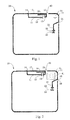
- Fig. 1 is a structural schematic diagram illustrating an antenna module, according to an exemplary embodiment.
- the antenna module may be applied in a mobile terminal, such as a smart mobile phone, and a tablet computer. As shown in Fig. 1 , the antenna module includes a first antenna 11 and a second antenna 21.
- a first ground point 12 of the first antenna 11 is electrically connected to a first section 17 of a metal frame of a mobile terminal via a first connection point 14, a first feed point 13 of the first antenna 11 is electrically connected to the first section 17 of the metal frame via a second connection point 15, and the first feed point 13, the first section 17 of the metal frame, and the first ground point 14 form a first loop.
- the first antenna 11 may radiate more radiation energy to outside via the first loop.
- the second antenna 21 is electrically connected to a second section 27 of the metal frame of the mobile terminal 10 via a third connection point 24, a slot 40 is opened between the second section 27 of the metal frame and the first section 17 of the metal frame, the second section 27 of the metal frame is electrically connected to a ground point of the mobile terminal 10 via a first contact point 31, a second feed point 23 of the second antenna 21 forms a second loop with the second section 27 of the metal frame and the ground point on the mobile terminal 10, and the second feed point 23 and a second ground point 22 of the second antenna 21 forms a third loop.
- the second antenna 21 may radiate more radiation energy to outside at two frequencies via the second and third loops respectively.
- the second section 27 of the metal frame is electrically connected to the ground point of the mobile terminal 10 via the first contact point 31, thus the second section 27 of the metal frame may tune a resonance frequency of the second antenna 21, and may reduce cross-talk to the first antenna 11 by the second antenna 21, thereby ensuring an isolation between the first antenna 11 and the second antenna 21.
- the first contact point may be electrically connected to the ground point of the mobile terminal via a metal casing of an audio socket of the terminal mobile.
- a discharge capacitor may be connected between the first contact point and the metal casing.
- the second section of the metal frame may also be electrically connected with the metal casing via a second contact point, and the second contact point is provided at an outside of the audio socket.
- the second section of the metal frame may also be electrically connected with the metal casing via a third contact point, and the third contact point is provided at another outside of the audio socket.
- the ground point of the mobile terminal may be a ground point of a PCB board on the mobile terminal.
- the first antenna may be a diversity antenna
- the second antenna may be a wifi antenna
- the antenna module provided by embodiments of the present invention may reduce cross-talk between the first and second antennas, and ensure an isolation between the first and second antennas.
- Fig. 2 is a structural schematic diagram illustrating an antenna module, according to a first exemplary embodiment.
- the first antenna 11 may be a LTE MIMO diversity antenna (short for diversity antenna below), and the frequency scope of the diversity antenna is 700MHz ⁇ 2700MHz.
- the second antenna 21 shown at the right side of Fig. 3 may be a wifi antenna, and a distance between the diversity antenna and the wifi antenna is a width of a slot 40 therebetween.
- the width of the slot is 1mm.
- the wifi antenna adopts a dual-loop antenna
- the second feed point 23 is below the second antenna 21
- a metal broken ring 20 at the right side is used as a main radiator
- the LTE MIMO diversity antenna adopts a structure of a single loop added with a parasitic element 16.
- Fig. 2 is only illustrative, and does not tend to restrict the present invention, and the present invention may also be applied to other antennas on the mobile terminal 10.
- the second section 27 of the metal frame is electrically connected to a ground point of PCB board 41 on the mobile terminal 10 via the first contact point 31.
- a discharge capacitor (not shown in the drawings) is connected between the first contact point 31 and the PCB board 41.
- an inductor (not shown in the drawings) may be connected between the first contact point 31 and the PCB board 41. The discharge capacitor and the inductor may tune the second antenna 21 to a specific resonance frequency, thus the audio socket 51, the PCB board 41 and the like, after being integrated, may be adaptable to antennas having different resonance frequencies.
- Fig. 3 is a structural schematic diagram illustrating an antenna module, according to a second exemplary embodiment.
- the ground point of the mobile terminal 10 may be a ground point of the PCB board 41 on the mobile terminal 10
- the second section 27 of the metal frame is electrically connected to the ground point of the PCB board 41 via a metal casing (not shown in the drawings) of an audio socket 51 of the mobile terminal 10.
- the audio socket 51 is above an area of the second antenna 21.
- the audio socket 51 by designing the audio socket 51 to be a metal casing and is grounded via the PCB board 41, unnecessary interference to the first antenna 11 and the second antenna 21 by high-order mode of inherent resonance inside the audio socket 51 may be avoided, unnecessary frequency offset of the antenna of the first antenna 11 and the second antenna 21 are avoided, and thus the antenna performance is improved.
- the second section 27 of the metal frame may be provided with a second touch point 32 and a third touch point 33, and both the second touch point 32 and the third touch point 33 are electrically connected to the metal casing of the audio socket 51.
- the second touch point 32 on the second section 27 of the metal frame, an interference to the first antenna 11 and the second antenna 21 by self-resonance of the audio socket 51 may be weakened, and by providing the third touch point 33 on the second section 27 of the metal frame, the isolation between the first antenna 11 and the second antenna 21 may be further enhanced, and a frequency offset phenomenon of the first antenna 11 and the second antenna 21 may be avoided after inserting the audio socket 51 into the mobile terminal 10.
- both the second touch point 32 and the third touch point 33 are electrically connected to the metal casing of the audio socket 51, and the audio socket 51 makes the metal casing to be grounded, which weakens the interference to the first antenna 11 and the second antenna 21 by self-resonance of the audio socket 51, and enhances the isolation between the wifi antenna and the diversity antenna.
- Fig. 4A is a schematic diagram illustrating a test result of a first antenna, according to an exemplary embodiment. As shown in Fig. 4A , an abscissa axis represents a frequency, and a vertical axis represents a cross-talk induced to the first antenna 11 by the second antenna 21, the unit thereof is decibel (dB).
- dB decibel
- the first antenna 11 is a diversity antenna, at a position in which a symbol " ⁇ " is labeled as 1, a frequency corresponding to the abscissa axis is 2.4GHZ, and a value corresponding to the vertical axis is -16.205dB; at a position in which a symbol " ⁇ " is labeled as 2, a frequency corresponding to the abscissa axis is 2.5GHZ, and a value corresponding to the vertical axis is -9.3160dB; at a position in which a symbol " ⁇ ” is labeled as 3, a frequency corresponding to the abscissa axis is 5.15GHZ, and a value corresponding to the vertical axis is -10.371dB; and at a position in which a symbol " ⁇ " is labeled as 4, a frequency corresponding to the abscissa axis is 5.8GHZ, and a value corresponding to the vertical axis is -25.938dB.
- the loss of the diversity antenna reaches the minimum at a point (between label 1 and label 2) of a first resonance frequency (about 2.4GHz) of the diversity antenna, and the loss value is lower than -16dB.
- the diversity antenna may also reaches a relative small loss at a point (corresponding to a vicinity of label 4) of a second resonance frequency (about 5.8GHz) of the diversity antenna, and the loss value is lower than a value of -25.938dB corresponding to the label 4. From above, the present invention may greatly reduce the cross-talk to the diversity antenna by the wifi antenna, thereby the diversity antenna may radiate more radiation energy to outside via the first loop.
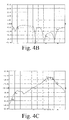
- Fig. 4B is a schematic diagram illustrating a test result of a second antenna, according to an exemplary embodiment. As shown in Fig. 4B , an abscissa axis represents a frequency, and a vertical axis represents a cross-talk induced to the second antenna 21 by the first antenna 11, the unit thereof is decibel (dB).
- dB decibel
- the second antenna 21 is a diversity antenna, at a position in which a symbol " ⁇ " is labeled as 5, a frequency corresponding to the abscissa axis is 770MHZ, and a value corresponding to the vertical axis is -4.7798dB; at a position in which a symbol " ⁇ " is labeled as 6, a frequency corresponding to the abscissa axis is 960MHZ, and a value corresponding to the vertical axis is -3.6482dB; at a position in which a symbol " ⁇ ” is labeled as 7, a frequency corresponding to the abscissa axis is 1.7082GHZ, and a value corresponding to the vertical axis is -25.202dB; at a position in which a symbol " ⁇ ” is labeled as 8, a frequency corresponding to the abscissa axis is 2.17GHZ, and a value corresponding to the vertical axis is -15.382dB; at
- the wifi antenna reaches the minimum loss at a point (corresponding to a position of label 7) of a third resonance frequency (about 1.7082GHz) of the wifi antenna, and the loss value reaches -25dB.
- the wifi antenna may also reaches a relative small loss at a point (corresponding to a position before label 8) of a fourth resonance frequency (lower than the frequency of 2.17GHz corresponding to the label 8) of the wifi antenna. From above, the present invention may greatly reduce the cross-talk to the wifi antenna by the diversity antenna, thereby the wifi antenna may radiate more radiation energy to outside via the second and third loops.
- Fig. 4C is a schematic diagram illustrating a test result of an insolation between the first antenna and the second antenna, according to an exemplary embodiment.
- an abscissa axis represents a frequency
- a vertical axis represents an isolation between the first antenna 11 and second antenna 21, the unit thereof is decibel (dB).
- the isolation between the diversity antenna and the wifi antenna is always below -15dB. From above, the present invention may greatly reduce the isolation between the first antenna and the second antenna.
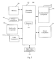
- Fig. 5 is a block diagram illustrating a mobile terminal, according to an exemplary embodiment.
- the device 500 may be a mobile phone, a computer, a digital broadcast terminal, a messaging device, a gaming console, a tablet, a medical device, exercise equipment, a personal digital assistant, and the like.
- the device 500 may include one or more of the following components: a processing component 502, a memory 504, a power component 506, a multimedia component 508, an audio component 510, an input/output (I/O) interface 512, a sensor component 514, and a communication component 516.
- the processing component 502 typically controls overall operations of the device 500, such as the operations associated with display, telephone calls, data communications, camera operations, and recording operations.
- the processing component 502 may include one or more processors 520 to execute instructions to perform all or part of the steps in the above described methods.
- the processing component 502 may include one or more modules which facilitate the interaction between the processing component 502 and other components.
- the processing component 502 may include a multimedia module to facilitate the interaction between the multimedia component 508 and the processing component 502.
- the memory 504 is configured to store various types of data to support the operation of the device 500. Examples of such data include instructions for any applications or methods operated on the device 500, contact data, phonebook data, messages, pictures, video, etc.
- the memory 504 may be implemented using any type of volatile or non-volatile memory devices, or a combination thereof, such as a static random access memory (SRAM), an electrically erasable programmable read-only memory (EEPROM), an erasable programmable read-only memory (EPROM), a programmable read-only memory (PROM), a read-only memory (ROM), a magnetic memory, a flash memory, a magnetic or optical disk.
- SRAM static random access memory
- EEPROM electrically erasable programmable read-only memory
- EPROM erasable programmable read-only memory
- PROM programmable read-only memory
- ROM read-only memory
- magnetic memory a magnetic memory
- flash memory a flash memory
- magnetic or optical disk a magnetic or optical
- the power component 506 provides power to various components of the device 500.
- the power component 506 may include a power management system, one or more power sources, and any other components associated with the generation, management, and distribution of power in the device 500.
- the multimedia component 508 includes a screen providing an output interface between the device 500 and the user.
- the screen may include a liquid crystal display (LCD) and a touch panel (TP). If the screen includes the touch panel, the screen may be implemented as a touch screen to receive input signals from the user.
- the touch panel includes one or more touch sensors to sense touches, swipes, and gestures on the touch panel. The touch sensors may not only sense a boundary of a touch or swipe action, but also sense a period of time and a pressure associated with the touch or swipe action.
- the multimedia component 508 includes a front camera and/or a rear camera. The front camera and the rear camera may receive an external multimedia datum while the device 500 is in an operation mode, such as a photographing mode or a video mode. Each of the front camera and the rear camera may be a fixed optical lens system or have focus and optical zoom capability.
- the audio component 510 is configured to output and/or input audio signals.
- the audio component 510 includes a microphone ("MIC") configured to receive an external audio signal when the device 500 is in an operation mode, such as a call mode, a recording mode, and a voice recognition mode.
- the received audio signal may be further stored in the memory 504 or transmitted via the communication component 516.
- the audio component 510 further includes a speaker to output audio signals.
- the I/O interface 512 provides an interface between the processing component 502 and peripheral interface modules, such as a keyboard, a click wheel, buttons, and the like.
- the buttons may include, but are not limited to, a home button, a volume button, a starting button, and a locking button.
- the sensor component 514 includes one or more sensors to provide status assessments of various aspects of the device 500. For instance, the sensor component 514 may detect an open/closed status of the device 500, relative positioning of components, e.g., the display and the keypad, of the device 500, a change in position of the device 500 or a component of the device 500, a presence or absence of user contact with the device 500, an orientation or an acceleration/deceleration of the device 500, and a change in temperature of the device 500.
- the sensor component 514 may include a proximity sensor configured to detect the presence of nearby objects without any physical contact.
- the sensor component 514 may also include a light sensor, such as a CMOS or CCD image sensor, for use in imaging applications.
- the sensor component 514 may also include an accelerometer sensor, a gyroscope sensor, a magnetic sensor, a pressure sensor, or a temperature sensor.
- the communication component 516 is configured to facilitate communication, wired or wirelessly, between the device 500 and other devices.
- the device 500 can access a wireless network based on a communication standard, such as WiFi, 2G, or 3G, or a combination thereof.
- the communication component 516 receives a broadcast signal or broadcast associated information from an external broadcast management system via a broadcast channel.
- the communication component 516 further includes a near field communication (NFC) module to facilitate short-range communications.
- the NFC module may be implemented based on a radio frequency identification (RFID) technology, an infrared data association (IrDA) technology, an ultra-wideband (UWB) technology, a Bluetooth (BT) technology, and other technologies.
- RFID radio frequency identification
- IrDA infrared data association
- UWB ultra-wideband
- BT Bluetooth
- the device 500 may be implemented with one or more application specific integrated circuits (ASICs), digital signal processors (DSPs), digital signal processing devices (DSPDs), programmable logic devices (PLDs), field programmable gate arrays (FPGAs), controllers, micro-controllers, microprocessors, or other electronic components, for performing the above described methods.
- ASICs application specific integrated circuits
- DSPs digital signal processors
- DSPDs digital signal processing devices
- PLDs programmable logic devices
- FPGAs field programmable gate arrays
- controllers micro-controllers, microprocessors, or other electronic components, for performing the above described methods.
Landscapes
- Engineering & Computer Science (AREA)
- Computer Hardware Design (AREA)
- Computer Networks & Wireless Communication (AREA)
- General Engineering & Computer Science (AREA)
- Support Of Aerials (AREA)
- Details Of Aerials (AREA)
- Telephone Set Structure (AREA)
- Microelectronics & Electronic Packaging (AREA)
Abstract
Description
- The present invention generally relates to field of communication technology, and more particularly, to an antenna module and a mobile terminal.
- With the development of Carrier Aggregation (CA) technology, it is possible to design more antennas in a mobile phone, and more antennas may enable the mobile phone to receive different kinds of wireless signals. In a typical layout of a metal frame antenna covering a Long Term Evolution (LTE) frequency band, a LTE Multiple-Input Multiple-Output (short for MIMO) diversity antenna and a wifi antenna are generally integrated in the same mobile terminal, and if a distance between the two antennas is relatively short, a serious coupling will occur between the two antennas, which affects a receiving performance of the antenna.
- In order to solve the problems in the related art, the embodiments of the present invention provide an antenna module and a mobile terminal for improving receiving performance of the antennas of the mobile terminal.
- According to a first aspect of embodiments of the present invention, there is provided an antenna module configured to be applied in a metal terminal, the antenna module includes: a first antenna and a second antenna;
a first ground point of the first antenna is electrically connected to a first section of a metal frame of the mobile terminal via a first connection point, and a first feed point of the first antenna is electrically connected to the first section of the metal frame via a second connection point; and
the second antenna is electrically connected to a second section of the metal frame of the mobile terminal via a third connection point, a slot is opened between the second section of the metal frame and the first section of the metal frame, and the second section of the metal frame is electrically connected to a ground point of the mobile terminal via a first contact point. - In one embodiment, the first contact point may be electrically connected to the ground point of the mobile terminal via a metal casing of an audio socket of the terminal mobile.
- In one embodiment, a discharge capacitor is connected between the first contact point and the metal casing.
- In one embodiment, the second section of the metal frame may also be electrically connected with the metal casing via a second contact point, and the second contact point is provided at one outer side of the audio socket.
- In one embodiment, the second section of the metal frame may also be electrically connected with the metal casing via a third contact point, and the third contact point is provided at another outer side of the audio socket.
- In one embodiment, the ground point of the mobile terminal may be a ground point of a PCB board on the mobile terminal.
- In one embodiment, the first antenna may be a diversity antenna, and the second antenna may be a wifi antenna.
- According to a second aspect of embodiments of the present invention, there is provided a mobile terminal, including:
- a processor; and
- a memory for storing instructions executable by the processor;
- wherein the mobile terminal further includes an antenna module which is configured as:
- a first antenna and a second antenna;
- a first ground point of the first antenna is electrically connected to a first section of a metal frame of the mobile terminal via a first connection point, and a first feed point of the first antenna is electrically connected to the first section of the metal frame via a second connection point; and
- the second antenna is electrically connected to a second section of the metal frame of the mobile terminal via a third connection point, a slot is opened between the second section of the metal frame and the first section of the metal frame, and the second section of the metal frame is electrically connected to a ground point of the mobile terminal.
- The technical solutions provided by embodiments of the present invention may have the following beneficial effects: the second section of the metal frame is electrically connected to the ground point of the mobile terminal via the first contact point, thus may tune a resonance frequency of the second antenna, and may reduce cross-talk generated by the second antenna to the first antenna, thereby ensuring the isolation between the first and second antennas.
- It is to be understood that both the foregoing general description and the following detailed description are exemplary and explanatory only and are not restrictive of the invention, as claimed.
- The accompanying drawings, which are incorporated in and constitute a part of this specification, illustrate embodiments consistent with the invention and, together with the description, serve to explain the principles of the invention.
-
Fig. 1 is a structural schematic diagram illustrating an antenna module, according to an exemplary embodiment. -
Fig. 2 is a structural schematic diagram illustrating an antenna module, according to a first exemplary embodiment. -
Fig. 3 is a structural schematic diagram illustrating an antenna module, according to a second exemplary embodiment. -
Fig. 4A is a schematic diagram illustrating a test result of a first antenna, according to an exemplary embodiment. -
Fig. 4B is a schematic diagram illustrating a test result of a second antenna, according to an exemplary embodiment. -
Fig. 4C is a schematic diagram illustrating a test result of an insolation between the first antenna and the second antenna, according to an exemplary embodiment. -
Fig. 5 is a block diagram illustrating a mobile terminal, according to an exemplary embodiment. - Reference will now be made in detail to exemplary embodiments, examples of which are illustrated in the accompanying drawings. The following description refers to the accompanying drawings in which the same numbers in different drawings represent the same or similar elements unless otherwise represented. The implementations set forth in the following description of exemplary embodiments do not represent all implementations consistent with the invention. Instead, they are merely examples of apparatuses and methods consistent with aspects related to the invention as recited in the appended claims.
-
Fig. 1 is a structural schematic diagram illustrating an antenna module, according to an exemplary embodiment. The antenna module may be applied in a mobile terminal, such as a smart mobile phone, and a tablet computer. As shown inFig. 1 , the antenna module includes afirst antenna 11 and asecond antenna 21. - A
first ground point 12 of thefirst antenna 11 is electrically connected to afirst section 17 of a metal frame of a mobile terminal via afirst connection point 14, afirst feed point 13 of thefirst antenna 11 is electrically connected to thefirst section 17 of the metal frame via asecond connection point 15, and thefirst feed point 13, thefirst section 17 of the metal frame, and thefirst ground point 14 form a first loop. Thefirst antenna 11 may radiate more radiation energy to outside via the first loop. - The
second antenna 21 is electrically connected to asecond section 27 of the metal frame of themobile terminal 10 via athird connection point 24, aslot 40 is opened between thesecond section 27 of the metal frame and thefirst section 17 of the metal frame, thesecond section 27 of the metal frame is electrically connected to a ground point of themobile terminal 10 via afirst contact point 31, asecond feed point 23 of thesecond antenna 21 forms a second loop with thesecond section 27 of the metal frame and the ground point on themobile terminal 10, and thesecond feed point 23 and asecond ground point 22 of thesecond antenna 21 forms a third loop. Thesecond antenna 21 may radiate more radiation energy to outside at two frequencies via the second and third loops respectively. - In the present embodiment, the
second section 27 of the metal frame is electrically connected to the ground point of themobile terminal 10 via thefirst contact point 31, thus thesecond section 27 of the metal frame may tune a resonance frequency of thesecond antenna 21, and may reduce cross-talk to thefirst antenna 11 by thesecond antenna 21, thereby ensuring an isolation between thefirst antenna 11 and thesecond antenna 21. - In one embodiment, the first contact point may be electrically connected to the ground point of the mobile terminal via a metal casing of an audio socket of the terminal mobile.
- In one embodiment, a discharge capacitor may be connected between the first contact point and the metal casing.
- In one embodiment, the second section of the metal frame may also be electrically connected with the metal casing via a second contact point, and the second contact point is provided at an outside of the audio socket.
- In one embodiment, the second section of the metal frame may also be electrically connected with the metal casing via a third contact point, and the third contact point is provided at another outside of the audio socket.
- In one embodiment, the ground point of the mobile terminal may be a ground point of a PCB board on the mobile terminal.
- In one embodiment, the first antenna may be a diversity antenna, and the second antenna may be a wifi antenna.
- So far the antenna module provided by embodiments of the present invention may reduce cross-talk between the first and second antennas, and ensure an isolation between the first and second antennas.
- Hereinafter, the technical solutions provided by embodiments of the present invention will be illustrated by specific embodiments.
-
Fig. 2 is a structural schematic diagram illustrating an antenna module, according to a first exemplary embodiment. On the basis of the embodiment shown in the aboveFig. 1 , as shown inFig. 2 , thefirst antenna 11 may be a LTE MIMO diversity antenna (short for diversity antenna below), and the frequency scope of the diversity antenna is 700MHz∼2700MHz. Thesecond antenna 21 shown at the right side ofFig. 3 may be a wifi antenna, and a distance between the diversity antenna and the wifi antenna is a width of aslot 40 therebetween. For example, the width of the slot is 1mm. The wifi antenna adopts a dual-loop antenna, thesecond feed point 23 is below thesecond antenna 21, a metalbroken ring 20 at the right side is used as a main radiator, and the LTE MIMO diversity antenna adopts a structure of a single loop added with aparasitic element 16. The person skilled in the art may understand thatFig. 2 is only illustrative, and does not tend to restrict the present invention, and the present invention may also be applied to other antennas on themobile terminal 10. - As shown in
Fig. 2 , thesecond section 27 of the metal frame is electrically connected to a ground point ofPCB board 41 on themobile terminal 10 via thefirst contact point 31. In an embodiment, a discharge capacitor (not shown in the drawings) is connected between thefirst contact point 31 and thePCB board 41. Alternatively, an inductor (not shown in the drawings) may be connected between thefirst contact point 31 and thePCB board 41. The discharge capacitor and the inductor may tune thesecond antenna 21 to a specific resonance frequency, thus theaudio socket 51, thePCB board 41 and the like, after being integrated, may be adaptable to antennas having different resonance frequencies. -
Fig. 3 is a structural schematic diagram illustrating an antenna module, according to a second exemplary embodiment. On the basis of the embodiment shown in the aboveFig. 1 or Fig. 2 , as shown inFig. 3 , in an embodiment, the ground point of themobile terminal 10 may be a ground point of thePCB board 41 on themobile terminal 10, thesecond section 27 of the metal frame is electrically connected to the ground point of thePCB board 41 via a metal casing (not shown in the drawings) of anaudio socket 51 of themobile terminal 10. In an embodiment, theaudio socket 51 is above an area of thesecond antenna 21. - In an embodiment, by designing the
audio socket 51 to be a metal casing and is grounded via thePCB board 41, unnecessary interference to thefirst antenna 11 and thesecond antenna 21 by high-order mode of inherent resonance inside theaudio socket 51 may be avoided, unnecessary frequency offset of the antenna of thefirst antenna 11 and thesecond antenna 21 are avoided, and thus the antenna performance is improved. - In an embodiment, the
second section 27 of the metal frame may be provided with asecond touch point 32 and athird touch point 33, and both thesecond touch point 32 and thethird touch point 33 are electrically connected to the metal casing of theaudio socket 51. By providing thesecond touch point 32 on thesecond section 27 of the metal frame, an interference to thefirst antenna 11 and thesecond antenna 21 by self-resonance of theaudio socket 51 may be weakened, and by providing thethird touch point 33 on thesecond section 27 of the metal frame, the isolation between thefirst antenna 11 and thesecond antenna 21 may be further enhanced, and a frequency offset phenomenon of thefirst antenna 11 and thesecond antenna 21 may be avoided after inserting theaudio socket 51 into themobile terminal 10. - In the present embodiment, both the
second touch point 32 and thethird touch point 33 are electrically connected to the metal casing of theaudio socket 51, and theaudio socket 51 makes the metal casing to be grounded, which weakens the interference to thefirst antenna 11 and thesecond antenna 21 by self-resonance of theaudio socket 51, and enhances the isolation between the wifi antenna and the diversity antenna. - In order to explain the advantageous technical effects of embodiments of the present invention more clearly, hereinafter, advantageous technical effects of embodiments of the present invention will be explained in detail by combining
Figs. 4A-4C . -
Fig. 4A is a schematic diagram illustrating a test result of a first antenna, according to an exemplary embodiment. As shown inFig. 4A , an abscissa axis represents a frequency, and a vertical axis represents a cross-talk induced to thefirst antenna 11 by thesecond antenna 21, the unit thereof is decibel (dB). When thefirst antenna 11 is a diversity antenna, at a position in which a symbol "Δ" is labeled as 1, a frequency corresponding to the abscissa axis is 2.4GHZ, and a value corresponding to the vertical axis is -16.205dB; at a position in which a symbol "Δ" is labeled as 2, a frequency corresponding to the abscissa axis is 2.5GHZ, and a value corresponding to the vertical axis is -9.3160dB; at a position in which a symbol "Δ" is labeled as 3, a frequency corresponding to the abscissa axis is 5.15GHZ, and a value corresponding to the vertical axis is -10.371dB; and at a position in which a symbol "Δ" is labeled as 4, a frequency corresponding to the abscissa axis is 5.8GHZ, and a value corresponding to the vertical axis is -25.938dB. The loss of the diversity antenna reaches the minimum at a point (betweenlabel 1 and label 2) of a first resonance frequency (about 2.4GHz) of the diversity antenna, and the loss value is lower than -16dB. The diversity antenna may also reaches a relative small loss at a point (corresponding to a vicinity of label 4) of a second resonance frequency (about 5.8GHz) of the diversity antenna, and the loss value is lower than a value of -25.938dB corresponding to the label 4. From above, the present invention may greatly reduce the cross-talk to the diversity antenna by the wifi antenna, thereby the diversity antenna may radiate more radiation energy to outside via the first loop. -
Fig. 4B is a schematic diagram illustrating a test result of a second antenna, according to an exemplary embodiment. As shown inFig. 4B , an abscissa axis represents a frequency, and a vertical axis represents a cross-talk induced to thesecond antenna 21 by thefirst antenna 11, the unit thereof is decibel (dB). When thesecond antenna 21 is a diversity antenna, at a position in which a symbol "Δ" is labeled as 5, a frequency corresponding to the abscissa axis is 770MHZ, and a value corresponding to the vertical axis is -4.7798dB; at a position in which a symbol "Δ" is labeled as 6, a frequency corresponding to the abscissa axis is 960MHZ, and a value corresponding to the vertical axis is -3.6482dB; at a position in which a symbol "Δ" is labeled as 7, a frequency corresponding to the abscissa axis is 1.7082GHZ, and a value corresponding to the vertical axis is -25.202dB; at a position in which a symbol "Δ" is labeled as 8, a frequency corresponding to the abscissa axis is 2.17GHZ, and a value corresponding to the vertical axis is -15.382dB; at a position in which a symbol "Δ" is labeled as 9, a frequency corresponding to the abscissa axis is 2.69GHZ, and a value corresponding to the vertical axis is -8.2518dB. - The wifi antenna reaches the minimum loss at a point (corresponding to a position of label 7) of a third resonance frequency (about 1.7082GHz) of the wifi antenna, and the loss value reaches -25dB. The wifi antenna may also reaches a relative small loss at a point (corresponding to a position before label 8) of a fourth resonance frequency (lower than the frequency of 2.17GHz corresponding to the label 8) of the wifi antenna. From above, the present invention may greatly reduce the cross-talk to the wifi antenna by the diversity antenna, thereby the wifi antenna may radiate more radiation energy to outside via the second and third loops.
-
Fig. 4C is a schematic diagram illustrating a test result of an insolation between the first antenna and the second antenna, according to an exemplary embodiment. As shown inFig. 4C , an abscissa axis represents a frequency, and a vertical axis represents an isolation between thefirst antenna 11 andsecond antenna 21, the unit thereof is decibel (dB). At a position in which a symbol "Δ" is labeled as 10, a frequency corresponding to the abscissa axis is 820MHZ, and a value corresponding to the vertical axis is -42.355dB; at a position in which a symbol "Δ" is labeled as 11, a frequency corresponding to the abscissa axis is 960MHZ, and a value corresponding to the vertical axis is -34.734dB; at a position in which a symbol "Δ" is labeled as 12, a frequency corresponding to the abscissa axis is 1.71GHZ, and a value corresponding to the vertical axis is -28.973dB; at a position in which a symbol "Δ" is labeled as 13, a frequency corresponding to the abscissa axis is 2.17GHZ, and a value corresponding to the vertical axis is -19.948dB; at a position in which a symbol "Δ" is labeled as 14, a frequency corresponding to the abscissa axis is 2.3GHZ, and a value corresponding to the vertical axis is -17.633dB; at a position in which a symbol "Δ" is labeled as 15, a frequency corresponding to the abscissa axis is 2.4GHZ, and a value corresponding to the vertical axis is -17.447dB; at a position in which a symbol "Δ" is labeled as 16, a frequency corresponding to the abscissa axis is 2.49GHZ, and a value corresponding to the vertical axis is -18.125dB; and at a position in which a symbol "Δ" is labeled as 17, a frequency corresponding to the abscissa axis is 2.69GHZ, and a value corresponding to the vertical axis is -25.398dB. - From above, within the frequency band of 700-2.69GHz, the isolation between the diversity antenna and the wifi antenna is always below -15dB. From above, the present invention may greatly reduce the isolation between the first antenna and the second antenna.
-
Fig. 5 is a block diagram illustrating a mobile terminal, according to an exemplary embodiment. For example, thedevice 500 may be a mobile phone, a computer, a digital broadcast terminal, a messaging device, a gaming console, a tablet, a medical device, exercise equipment, a personal digital assistant, and the like. - Referring to
Fig. 5 , thedevice 500 may include one or more of the following components: aprocessing component 502, amemory 504, apower component 506, amultimedia component 508, anaudio component 510, an input/output (I/O)interface 512, asensor component 514, and acommunication component 516. - The
processing component 502 typically controls overall operations of thedevice 500, such as the operations associated with display, telephone calls, data communications, camera operations, and recording operations. Theprocessing component 502 may include one ormore processors 520 to execute instructions to perform all or part of the steps in the above described methods. Moreover, theprocessing component 502 may include one or more modules which facilitate the interaction between theprocessing component 502 and other components. For instance, theprocessing component 502 may include a multimedia module to facilitate the interaction between themultimedia component 508 and theprocessing component 502. - The
memory 504 is configured to store various types of data to support the operation of thedevice 500. Examples of such data include instructions for any applications or methods operated on thedevice 500, contact data, phonebook data, messages, pictures, video, etc. Thememory 504 may be implemented using any type of volatile or non-volatile memory devices, or a combination thereof, such as a static random access memory (SRAM), an electrically erasable programmable read-only memory (EEPROM), an erasable programmable read-only memory (EPROM), a programmable read-only memory (PROM), a read-only memory (ROM), a magnetic memory, a flash memory, a magnetic or optical disk. - The
power component 506 provides power to various components of thedevice 500. Thepower component 506 may include a power management system, one or more power sources, and any other components associated with the generation, management, and distribution of power in thedevice 500. - The
multimedia component 508 includes a screen providing an output interface between thedevice 500 and the user. In some embodiments, the screen may include a liquid crystal display (LCD) and a touch panel (TP). If the screen includes the touch panel, the screen may be implemented as a touch screen to receive input signals from the user. The touch panel includes one or more touch sensors to sense touches, swipes, and gestures on the touch panel. The touch sensors may not only sense a boundary of a touch or swipe action, but also sense a period of time and a pressure associated with the touch or swipe action. In some embodiments, themultimedia component 508 includes a front camera and/or a rear camera. The front camera and the rear camera may receive an external multimedia datum while thedevice 500 is in an operation mode, such as a photographing mode or a video mode. Each of the front camera and the rear camera may be a fixed optical lens system or have focus and optical zoom capability. - The
audio component 510 is configured to output and/or input audio signals. For example, theaudio component 510 includes a microphone ("MIC") configured to receive an external audio signal when thedevice 500 is in an operation mode, such as a call mode, a recording mode, and a voice recognition mode. The received audio signal may be further stored in thememory 504 or transmitted via thecommunication component 516. In some embodiments, theaudio component 510 further includes a speaker to output audio signals. - The I/
O interface 512 provides an interface between theprocessing component 502 and peripheral interface modules, such as a keyboard, a click wheel, buttons, and the like. The buttons may include, but are not limited to, a home button, a volume button, a starting button, and a locking button. - The
sensor component 514 includes one or more sensors to provide status assessments of various aspects of thedevice 500. For instance, thesensor component 514 may detect an open/closed status of thedevice 500, relative positioning of components, e.g., the display and the keypad, of thedevice 500, a change in position of thedevice 500 or a component of thedevice 500, a presence or absence of user contact with thedevice 500, an orientation or an acceleration/deceleration of thedevice 500, and a change in temperature of thedevice 500. Thesensor component 514 may include a proximity sensor configured to detect the presence of nearby objects without any physical contact. Thesensor component 514 may also include a light sensor, such as a CMOS or CCD image sensor, for use in imaging applications. In some embodiments, thesensor component 514 may also include an accelerometer sensor, a gyroscope sensor, a magnetic sensor, a pressure sensor, or a temperature sensor. - The
communication component 516 is configured to facilitate communication, wired or wirelessly, between thedevice 500 and other devices. Thedevice 500 can access a wireless network based on a communication standard, such as WiFi, 2G, or 3G, or a combination thereof. In one exemplary embodiment, thecommunication component 516 receives a broadcast signal or broadcast associated information from an external broadcast management system via a broadcast channel. In one exemplary embodiment, thecommunication component 516 further includes a near field communication (NFC) module to facilitate short-range communications. For example, the NFC module may be implemented based on a radio frequency identification (RFID) technology, an infrared data association (IrDA) technology, an ultra-wideband (UWB) technology, a Bluetooth (BT) technology, and other technologies. - In exemplary embodiments, the
device 500 may be implemented with one or more application specific integrated circuits (ASICs), digital signal processors (DSPs), digital signal processing devices (DSPDs), programmable logic devices (PLDs), field programmable gate arrays (FPGAs), controllers, micro-controllers, microprocessors, or other electronic components, for performing the above described methods.
Claims (8)
- An antenna module configured to be applied in a mobile terminal (10), characterized in that, the antenna module comprises: a first antenna (11) and a second antenna (21);
a first ground point (12) of the first antenna (11) is electrically connected to a first section (17) of a metal frame of the mobile terminal (10) via a first connection point (14), and a first feed point (13) of the first antenna (11) is electrically connected to the first section (17) of the metal frame via a second connection point (15); and
the second antenna (21) is electrically connected to a second section (27) of the metal frame of the mobile terminal (10) via a third connection point (24), a slot (40) is opened between the second section (27) of the metal frame and the first section (17) of the metal frame, and the second section (27) of the metal frame is electrically connected to a ground point of the mobile terminal (10) via a first contact point (31). - The antenna module of claim 1, characterized in that, the first contact point (17) is electrically connected to the ground point of the mobile terminal (10) via a metal casing of an audio socket of the terminal mobile (10).
- The antenna module of claim 2, characterized in that, a discharge capacitor is connected between the first contact point (17) and the metal casing.
- The antenna module of claim 2, characterized in that, the second section (27) of the metal frame is also electrically connected with the metal casing via a second contact point, and the second contact point is provided at one outer side of the audio socket.
- The antenna module of claim 2, characterized in that, the second section (27) of the metal frame is also electrically connected with the metal casing via a third contact point, and the third contact point is provided at another outer side of the audio socket.
- The antenna module of claim 2, characterized in that, the ground point of the mobile terminal (10) is a ground point of a PCB board on the mobile terminal (10).
- The antenna module of claim 1, characterized in that, the first antenna (11) is a diversity antenna, and the second antenna (12) is a wifi antenna.
- A mobile terminal (10), characterized in that, the mobile terminal (10) comprises:a processor (520); anda memory (504) for storing instructions executable by the processor (520);wherein the mobile terminal (10) further comprises an antenna module which is configured as:a first antenna (11) and a second antenna (12);a first ground point (12) of the first antenna (11) is electrically connected to a first section (17) of a metal frame of the mobile terminal (10) via a first connection point (14), and a first feed point (13) of the first antenna (11) is electrically connected to the first section (17) of the metal frame via a second connection point (15); andthe second antenna (21) is electrically connected to a second section (27) of the metal frame of the mobile terminal (10) via a third connection point (24), a slot (40) is opened between the second section (27) of the metal frame and the first section (17) of the metal frame, and the second section (27) of the metal frame is electrically connected to a ground point of the mobile terminal (10).
Applications Claiming Priority (1)
| Application Number | Priority Date | Filing Date | Title |
|---|---|---|---|
| CN201510073377.4A CN104577334B (en) | 2015-02-11 | 2015-02-11 | Anneta module and mobile terminal |
Publications (2)
| Publication Number | Publication Date |
|---|---|
| EP3057176A1 true EP3057176A1 (en) | 2016-08-17 |
| EP3057176B1 EP3057176B1 (en) | 2021-07-21 |
Family
ID=53092870
Family Applications (1)
| Application Number | Title | Priority Date | Filing Date |
|---|---|---|---|
| EP16155344.1A Active EP3057176B1 (en) | 2015-02-11 | 2016-02-11 | Antenna module and mobile terminal |
Country Status (8)
| Country | Link |
|---|---|
| US (1) | US10186755B2 (en) |
| EP (1) | EP3057176B1 (en) |
| JP (1) | JP6208384B2 (en) |
| KR (1) | KR101786756B1 (en) |
| CN (1) | CN104577334B (en) |
| MX (1) | MX358803B (en) |
| RU (1) | RU2627942C2 (en) |
| WO (1) | WO2016127668A1 (en) |
Cited By (6)
| Publication number | Priority date | Publication date | Assignee | Title |
|---|---|---|---|---|
| EP3179554A1 (en) * | 2015-12-03 | 2017-06-14 | Xiaomi Inc. | Terminal casing and terminal |
| EP3203577A3 (en) * | 2016-01-11 | 2017-11-01 | Samsung Electronics Co., Ltd | Electronic device including metal housing antenna |
| WO2019068331A1 (en) * | 2017-10-05 | 2019-04-11 | Huawei Technologies Co., Ltd. | Antenna system for a wireless communication device |
| EP3506422A1 (en) * | 2017-12-29 | 2019-07-03 | Guangdong Oppo Mobile Telecommunications Corp., Ltd | Antenna assembly and electronic apparatus |
| EP3383004A4 (en) * | 2015-11-27 | 2019-07-31 | LG Electronics Inc. -1- | MOBILE TERMINAL |
| US10498013B2 (en) | 2015-08-07 | 2019-12-03 | Microsoft Technology Licensing, Llc | Antenna arrangement for an electronic device |
Families Citing this family (50)
| Publication number | Priority date | Publication date | Assignee | Title |
|---|---|---|---|---|
| US10622702B2 (en) * | 2014-12-26 | 2020-04-14 | Byd Company Limited | Mobile terminal and antenna of mobile terminal |
| CN104577334B (en) | 2015-02-11 | 2017-07-21 | 小米科技有限责任公司 | Anneta module and mobile terminal |
| KR102352490B1 (en) | 2015-06-11 | 2022-01-18 | 삼성전자주식회사 | Antenna and electronic device comprising the same |
| CN105826680B (en) * | 2015-06-30 | 2019-07-26 | 维沃移动通信有限公司 | A kind of antenna system and electric terminal |
| CN105140623B (en) * | 2015-07-23 | 2018-03-27 | 广东欧珀移动通信有限公司 | Antenna system and communication terminal using the antenna system |
| US10224606B2 (en) * | 2015-07-30 | 2019-03-05 | Samsung Electro-Mechanics Co., Ltd. | Electronic device with multi-band antenna for supporting carrier aggregation using non-segmented conductive border member |
| CN106486757B (en) * | 2015-08-26 | 2021-01-15 | 小米科技有限责任公司 | Antenna, mobile terminal back cover and mobile terminal |
| CN105428792A (en) * | 2015-11-12 | 2016-03-23 | 深圳市天鼎微波科技有限公司 | Complete metal frame antenna |
| US10498038B2 (en) | 2015-11-27 | 2019-12-03 | Lg Electronics Inc. | Mobile terminal |
| CN107851884B (en) * | 2015-12-03 | 2020-06-02 | 华为技术有限公司 | Metal Frame Antennas and Terminal Equipment |
| CN108736144B (en) * | 2015-12-09 | 2020-09-18 | Oppo广东移动通信有限公司 | mobile terminal |
| CN105514604B (en) * | 2015-12-09 | 2018-09-11 | 广东欧珀移动通信有限公司 | Mobile terminal |
| CN105657091B (en) * | 2015-12-25 | 2019-03-08 | 宇龙计算机通信科技(深圳)有限公司 | A kind of mobile terminal based on no breakpoint metal center and metal back cover |
| CN105514577A (en) * | 2016-01-26 | 2016-04-20 | 广东欧珀移动通信有限公司 | A broadband multi-frequency mobile phone antenna and mobile terminal |
| CN107026671B (en) * | 2016-02-01 | 2020-03-17 | 北京小米移动软件有限公司 | Isolation control circuit and method and mobile terminal |
| CN107204512B (en) | 2016-03-16 | 2019-12-06 | 北京小米移动软件有限公司 | Antenna of mobile terminal and mobile terminal |
| CN107240765B (en) | 2016-03-29 | 2019-12-13 | 北京小米移动软件有限公司 | A WIFI antenna |
| CN107240760B (en) * | 2016-03-29 | 2019-11-15 | 北京小米移动软件有限公司 | An all-metal mobile phone antenna |
| CN105870593B (en) * | 2016-04-11 | 2019-02-26 | 上海安费诺永亿通讯电子有限公司 | A kind of high-isolation carrier wave polymerization antenna and electronic equipment |
| CN105958201B (en) * | 2016-04-27 | 2019-12-24 | 上海安费诺永亿通讯电子有限公司 | Metal frame cell-phone antenna |
| US11283154B2 (en) * | 2016-05-28 | 2022-03-22 | Huawei Device Co., Ltd. | Communications terminal |
| CN105977614B (en) * | 2016-05-30 | 2020-02-07 | 北京小米移动软件有限公司 | Communication antenna, control method and device of communication antenna and terminal |
| KR102534531B1 (en) * | 2016-07-29 | 2023-05-19 | 삼성전자주식회사 | Electronic device including multiple antennas |
| CN106058436A (en) * | 2016-08-04 | 2016-10-26 | 北京小米移动软件有限公司 | Antenna module and electronic equipment |
| CN106207491A (en) * | 2016-08-24 | 2016-12-07 | 北京小米移动软件有限公司 | device for WIFI MIMO |
| CN106410400B (en) * | 2016-10-18 | 2023-09-26 | 上海德门电子科技有限公司 | Communication equipment with metal shell and NFC structure thereof |
| US11011837B2 (en) | 2016-11-17 | 2021-05-18 | Huawei Technologies Co., Ltd. | Communications terminal |
| CN106654558B (en) * | 2016-12-19 | 2019-11-29 | 北京小米移动软件有限公司 | Mobile terminal antenna and its control method and device |
| CN113839208B (en) * | 2016-12-21 | 2024-10-22 | 宏达国际电子股份有限公司 | Mobile device |
| CN113067122B (en) * | 2017-01-26 | 2023-12-19 | Lg电子株式会社 | mobile terminal |
| KR102615122B1 (en) | 2017-02-24 | 2023-12-18 | 삼성전자주식회사 | Electronic device comprising antenna |
| AU2017405558B2 (en) * | 2017-03-20 | 2020-12-03 | Huawei Technologies Co., Ltd. | Antenna of mobile terminal and mobile terminal |
| CN106887678A (en) * | 2017-03-28 | 2017-06-23 | 维沃移动通信有限公司 | A kind of mobile terminal antenna and mobile terminal |
| CN107994318B (en) * | 2017-11-23 | 2020-06-02 | 北京小米移动软件有限公司 | Antenna module and electronic equipment |
| CN110034402B (en) * | 2018-01-11 | 2021-11-23 | 深圳富泰宏精密工业有限公司 | Antenna structure and wireless communication device with same |
| CN108271326B (en) * | 2018-01-16 | 2020-08-04 | Oppo广东移动通信有限公司 | Middle frame and electronic equipment |
| CN111213283B (en) * | 2018-05-15 | 2021-06-29 | 华为技术有限公司 | An antenna system and terminal equipment |
| CN108832297B (en) * | 2018-06-22 | 2021-05-07 | 维沃移动通信有限公司 | Antenna working method and mobile terminal |
| CN109103570B (en) * | 2018-08-03 | 2020-08-21 | 瑞声精密制造科技(常州)有限公司 | Loop antenna system and mobile terminal |
| CN109659693B (en) * | 2018-12-12 | 2021-08-24 | 维沃移动通信有限公司 | An antenna structure and communication terminal |
| KR102606428B1 (en) | 2019-02-19 | 2023-11-29 | 삼성전자주식회사 | A plurality of antennas and electronic device including the same |
| CN111668604B (en) * | 2019-03-08 | 2022-07-12 | Oppo广东移动通信有限公司 | Antenna components and electronic equipment |
| CN110247160B (en) * | 2019-04-30 | 2021-10-29 | 荣耀终端有限公司 | An antenna assembly and mobile terminal |
| CN112448140B (en) | 2019-08-30 | 2022-03-01 | 北京小米移动软件有限公司 | Antenna module and terminal |
| CN110890622B (en) * | 2019-09-23 | 2021-07-02 | 捷开通讯(深圳)有限公司 | Antenna device |
| TWI713254B (en) * | 2019-11-25 | 2020-12-11 | 和碩聯合科技股份有限公司 | Antenna module |
| CN113036433B (en) * | 2019-12-09 | 2022-08-19 | 北京小米移动软件有限公司 | Antenna structure and electronic device |
| CN116995414A (en) | 2020-05-27 | 2023-11-03 | 华为技术有限公司 | Electronic equipment |
| CN111816985B (en) * | 2020-06-10 | 2022-04-26 | 昆山睿翔讯通通信技术有限公司 | Antenna system suitable for mobile terminal in metal middle frame form and mobile terminal |
| EP4241335A4 (en) * | 2020-11-06 | 2024-07-10 | Dejero Labs Inc. | SYSTEM AND METHOD FOR MOUNTING ANTENNAS |
Citations (5)
| Publication number | Priority date | Publication date | Assignee | Title |
|---|---|---|---|---|
| US20090009401A1 (en) * | 2007-07-04 | 2009-01-08 | Kabushiki Kaisha Toshiba | Antenna device having no less than two antenna elements |
| US20090027286A1 (en) * | 2007-07-27 | 2009-01-29 | Kabushiki Kaisha Toshiba | Antenna apparatus and wireless device |
| EP2498336A2 (en) * | 2011-03-07 | 2012-09-12 | Apple Inc. | Tunable Antenna System with Receiver Diversity |
| US20130076580A1 (en) * | 2011-09-28 | 2013-03-28 | Shuai Zhang | Multi-Band Wireless Terminals With A Hybrid Antenna Along An End Portion, And Related Multi-Band Antenna Systems |
| EP2709209A1 (en) * | 2012-09-14 | 2014-03-19 | Acer Incorporated | Communication device and antenna system with high isolation |
Family Cites Families (75)
| Publication number | Priority date | Publication date | Assignee | Title |
|---|---|---|---|---|
| US20040257283A1 (en) * | 2003-06-19 | 2004-12-23 | International Business Machines Corporation | Antennas integrated with metallic display covers of computing devices |
| US7623079B2 (en) * | 2004-06-30 | 2009-11-24 | Denso Corporation | Vehicle antenna, monitor display device having vehicle antenna, an method of forming vehicle antenna |
| JP2006041826A (en) * | 2004-07-26 | 2006-02-09 | Matsushita Electric Ind Co Ltd | Mobile phone equipment |
| US7271769B2 (en) * | 2004-09-22 | 2007-09-18 | Lenovo (Singapore) Pte Ltd. | Antennas encapsulated within plastic display covers of computing devices |
| EP1843432B1 (en) * | 2005-01-27 | 2015-08-12 | Murata Manufacturing Co., Ltd. | Antenna and wireless communication device |
| JP4904895B2 (en) * | 2006-04-12 | 2012-03-28 | ソニー株式会社 | Antenna device |
| US8094859B2 (en) * | 2006-12-14 | 2012-01-10 | Sharp Kabushiki Kaisha | Dipole antenna device, earphone antenna device, and wireless communication terminal device connected to the device |
| JP4762126B2 (en) * | 2006-12-20 | 2011-08-31 | 株式会社東芝 | Electronics |
| JPWO2009022387A1 (en) | 2007-08-10 | 2010-11-11 | パナソニック株式会社 | Portable radio |
| US7551142B1 (en) * | 2007-12-13 | 2009-06-23 | Apple Inc. | Hybrid antennas with directly fed antenna slots for handheld electronic devices |
| JP2010041071A (en) | 2008-07-31 | 2010-02-18 | Toshiba Corp | Antenna device |
| US8656579B2 (en) * | 2008-08-29 | 2014-02-25 | Motorola Mobility Llc | Method of forming a housing with integral antenna |
| JP2010147636A (en) | 2008-12-17 | 2010-07-01 | Toshiba Corp | Antenna device and radio apparatus |
| CN102005640B (en) * | 2009-08-28 | 2015-04-15 | 深圳富泰宏精密工业有限公司 | Wireless communication device |
| US9252494B2 (en) * | 2009-11-13 | 2016-02-02 | Hitachi Metals, Ltd. | Frequency-variable antenna circuit, antenna device constituting it, and wireless communications apparatus comprising it |
| US8872706B2 (en) * | 2010-11-05 | 2014-10-28 | Apple Inc. | Antenna system with receiver diversity and tunable matching circuit |
| US8947302B2 (en) * | 2010-11-05 | 2015-02-03 | Apple Inc. | Antenna system with antenna swapping and antenna tuning |
| KR101801186B1 (en) | 2011-02-25 | 2017-11-24 | 엘지전자 주식회사 | Mobile terminal |
| KR101831644B1 (en) * | 2011-03-02 | 2018-02-23 | 삼성전자 주식회사 | Earphone having the touch input unit and a portable terminal using the same |
| KR101759994B1 (en) * | 2011-03-16 | 2017-07-20 | 엘지전자 주식회사 | Mobile terminal |
| KR101334812B1 (en) * | 2011-04-14 | 2013-11-28 | 삼성전자주식회사 | Antenna device for portable terminal |
| US9088069B2 (en) * | 2011-09-21 | 2015-07-21 | Sony Corporation | Wireless communication apparatus |
| KR101318877B1 (en) * | 2011-10-14 | 2013-10-17 | 삼성전자주식회사 | Portable terminal |
| US9160058B2 (en) * | 2011-11-28 | 2015-10-13 | Htc Corporation | Portable communication device |
| JP5861455B2 (en) * | 2011-12-28 | 2016-02-16 | ソニー株式会社 | Antenna device |
| US9059520B2 (en) * | 2012-01-31 | 2015-06-16 | Sony Corporation | Wireless communication device and communication terminal apparatus |
| CN102593578B (en) | 2012-03-12 | 2015-01-07 | 广东欧珀移动通信有限公司 | Coupling feed-in type antenna device for mobile phone |
| US8907853B2 (en) * | 2012-07-26 | 2014-12-09 | Sony Corporation | Wireless electronic devices with multiple curved antennas along an end portion, and related antenna systems |
| CN102800931A (en) | 2012-08-23 | 2012-11-28 | 广东欧珀移动通信有限公司 | Mobile communication terminal antenna device |
| KR102013588B1 (en) * | 2012-09-19 | 2019-08-23 | 엘지전자 주식회사 | Mobile terminal |
| TWI539656B (en) | 2012-10-19 | 2016-06-21 | 宏碁股份有限公司 | Mobile communication device |
| US9287612B2 (en) * | 2012-11-16 | 2016-03-15 | Sony Mobile Communications Ab | Transparent antennas for wireless terminals |
| CN103022689A (en) * | 2012-12-24 | 2013-04-03 | 上海安费诺永亿通讯电子有限公司 | Wide frequency antenna capable of serving as metal shell of mobile terminal |
| CN103067763B (en) * | 2012-12-25 | 2015-10-28 | 广东远峰电子科技有限公司 | TV box for improving wireless signal transmission efficiency |
| US9331397B2 (en) * | 2013-03-18 | 2016-05-03 | Apple Inc. | Tunable antenna with slot-based parasitic element |
| KR102002874B1 (en) * | 2013-03-28 | 2019-07-24 | 삼성전자주식회사 | Antenna device for portable terminal |
| KR101467196B1 (en) * | 2013-03-29 | 2014-12-01 | 주식회사 팬택 | Terminal including multiband antenna using conductive border |
| CN103296385B (en) * | 2013-05-29 | 2016-05-11 | 上海安费诺永亿通讯电子有限公司 | A kind of adjustable frequency antenna system |
| CN103326124B (en) | 2013-05-29 | 2015-04-01 | 上海安费诺永亿通讯电子有限公司 | Adjustable multi-band antenna system |
| TWI617085B (en) | 2013-05-31 | 2018-03-01 | 群邁通訊股份有限公司 | Antenna structure and wireless communication device using same |
| CN103346397B (en) | 2013-06-21 | 2016-01-13 | 上海安费诺永亿通讯电子有限公司 | Be applicable to the frequency antenna system with metal frame architecture mobile terminal |
| JP6184778B2 (en) * | 2013-07-08 | 2017-08-23 | シャープ株式会社 | Antenna element and antenna device |
| GB2516304A (en) * | 2013-07-19 | 2015-01-21 | Nokia Corp | Apparatus and methods for wireless communication |
| CN103390793A (en) * | 2013-07-29 | 2013-11-13 | 苏州维特比信息技术有限公司 | Mobile terminal using metal frame antenna |
| CN203536554U (en) * | 2013-09-16 | 2014-04-09 | 中兴通讯股份有限公司 | Metal frame antenna |
| US9711841B2 (en) * | 2013-09-20 | 2017-07-18 | Sony Corporation | Apparatus for tuning multi-band frame antenna |
| CN103606742B (en) * | 2013-10-18 | 2016-06-08 | 上海安费诺永亿通讯电子有限公司 | A kind of composite antenna for handset terminal |
| CN103607484B (en) * | 2013-11-05 | 2017-02-01 | 华为终端有限公司 | Wireless communication terminal |
| US20150123871A1 (en) * | 2013-11-06 | 2015-05-07 | Acer Incorporated | Mobile device and antenna structure with conductive frame |
| CN203589193U (en) | 2013-11-14 | 2014-05-07 | 深圳市威尔创通讯科技有限公司 | Wideband multitape coupled antenna structure based on mobile phone metal frame |
| CN104659483A (en) * | 2013-11-22 | 2015-05-27 | 英业达科技有限公司 | Electronic device |
| US9197270B2 (en) * | 2013-11-27 | 2015-11-24 | Sony Corporation | Double ring antenna with integrated non-cellular antennas |
| CN203850424U (en) * | 2014-03-31 | 2014-09-24 | 小米科技有限责任公司 | Loop antenna system with gaps participating in radiation |
| CN104064866B (en) * | 2014-05-26 | 2018-08-17 | 普尔思(苏州)无线通讯产品有限公司 | Applied to the antenna structure of mobile phole simultaneously with becket and all-metal rear shell |
| CN105226371B (en) * | 2014-05-26 | 2019-02-26 | 比亚迪股份有限公司 | Antenna system for electronic equipment and electronic equipment with the same |
| CN204144448U (en) * | 2014-08-04 | 2015-02-04 | 瑞声精密制造科技(常州)有限公司 | Mobile terminal device and antenna modules thereof |
| AU2015304148A1 (en) * | 2014-08-18 | 2017-02-02 | Samsung Electronics Co., Ltd. | Antenna of electronic device |
| KR102226173B1 (en) * | 2014-09-02 | 2021-03-10 | 삼성전자주식회사 | Antenna using exterior metal frame and electronic device therewith |
| US9647332B2 (en) * | 2014-09-03 | 2017-05-09 | Apple Inc. | Electronic device antenna with interference mitigation circuitry |
| US9537219B2 (en) * | 2014-09-29 | 2017-01-03 | Apple Inc. | Electronic device with passive antenna retuning circuitry |
| KR102242262B1 (en) * | 2014-10-24 | 2021-04-20 | 삼성전자주식회사 | Antenna for Using Coupling and Device thereof |
| KR20160069923A (en) * | 2014-12-09 | 2016-06-17 | 엘지전자 주식회사 | Antenna module and mobile terminal using the same |
| KR102176367B1 (en) * | 2015-01-05 | 2020-11-09 | 엘지전자 주식회사 | Antenna module and mobile terminal having the same |
| US9780452B2 (en) * | 2015-01-05 | 2017-10-03 | Sony Corporation | Communication terminal |
| KR102288451B1 (en) * | 2015-02-02 | 2021-08-10 | 삼성전자주식회사 | Antenna and electronic device therewith |
| CN104577334B (en) * | 2015-02-11 | 2017-07-21 | 小米科技有限责任公司 | Anneta module and mobile terminal |
| CN106450658A (en) * | 2015-08-07 | 2017-02-22 | 微软技术许可有限责任公司 | Antenna device for electronic equipment |
| KR102306080B1 (en) * | 2015-08-13 | 2021-09-30 | 삼성전자주식회사 | Antenna and electronic device including the antenna |
| KR102408870B1 (en) * | 2015-08-13 | 2022-06-15 | 삼성전자주식회사 | Antenna and electronic device having it |
| KR102447383B1 (en) * | 2015-08-13 | 2022-09-27 | 삼성전자주식회사 | Antenna device and electronic device comprising same |
| US10498038B2 (en) * | 2015-11-27 | 2019-12-03 | Lg Electronics Inc. | Mobile terminal |
| KR102476765B1 (en) * | 2015-12-15 | 2022-12-13 | 삼성전자주식회사 | Electronic Device with Antenna |
| KR102466002B1 (en) * | 2016-04-19 | 2022-11-11 | 삼성전자주식회사 | Electronic device including antenna |
| KR102578502B1 (en) * | 2016-08-01 | 2023-09-15 | 삼성전자주식회사 | Electronic device comprising antenna |
| US10211518B2 (en) * | 2016-12-07 | 2019-02-19 | Guangdong Oppo Mobile Telecommunications Corp., Ltd. | Mobile terminal |
-
2015
- 2015-02-11 CN CN201510073377.4A patent/CN104577334B/en active Active
- 2015-10-30 RU RU2016100189A patent/RU2627942C2/en active
- 2015-10-30 MX MX2016000250A patent/MX358803B/en active IP Right Grant
- 2015-10-30 JP JP2016574329A patent/JP6208384B2/en not_active Expired - Fee Related
- 2015-10-30 KR KR1020157036385A patent/KR101786756B1/en not_active Expired - Fee Related
- 2015-10-30 WO PCT/CN2015/093295 patent/WO2016127668A1/en not_active Ceased
-
2016
- 2016-02-08 US US15/018,114 patent/US10186755B2/en active Active
- 2016-02-11 EP EP16155344.1A patent/EP3057176B1/en active Active
Patent Citations (5)
| Publication number | Priority date | Publication date | Assignee | Title |
|---|---|---|---|---|
| US20090009401A1 (en) * | 2007-07-04 | 2009-01-08 | Kabushiki Kaisha Toshiba | Antenna device having no less than two antenna elements |
| US20090027286A1 (en) * | 2007-07-27 | 2009-01-29 | Kabushiki Kaisha Toshiba | Antenna apparatus and wireless device |
| EP2498336A2 (en) * | 2011-03-07 | 2012-09-12 | Apple Inc. | Tunable Antenna System with Receiver Diversity |
| US20130076580A1 (en) * | 2011-09-28 | 2013-03-28 | Shuai Zhang | Multi-Band Wireless Terminals With A Hybrid Antenna Along An End Portion, And Related Multi-Band Antenna Systems |
| EP2709209A1 (en) * | 2012-09-14 | 2014-03-19 | Acer Incorporated | Communication device and antenna system with high isolation |
Cited By (12)
| Publication number | Priority date | Publication date | Assignee | Title |
|---|---|---|---|---|
| US10498013B2 (en) | 2015-08-07 | 2019-12-03 | Microsoft Technology Licensing, Llc | Antenna arrangement for an electronic device |
| EP3383004A4 (en) * | 2015-11-27 | 2019-07-31 | LG Electronics Inc. -1- | MOBILE TERMINAL |
| EP3383003A4 (en) * | 2015-11-27 | 2019-07-31 | LG Electronics Inc. -1- | MOBILE TERMINAL |
| EP3996204A1 (en) * | 2015-11-27 | 2022-05-11 | LG Electronics Inc. | Mobile terminal |
| EP3179554A1 (en) * | 2015-12-03 | 2017-06-14 | Xiaomi Inc. | Terminal casing and terminal |
| US10522901B2 (en) | 2015-12-03 | 2019-12-31 | Xiaomi Inc. | Terminal casing and terminal |
| EP3203577A3 (en) * | 2016-01-11 | 2017-11-01 | Samsung Electronics Co., Ltd | Electronic device including metal housing antenna |
| US10283846B2 (en) | 2016-01-11 | 2019-05-07 | Samsung Electronics Co., Ltd. | Electronic device including metal housing antenna |
| WO2019068331A1 (en) * | 2017-10-05 | 2019-04-11 | Huawei Technologies Co., Ltd. | Antenna system for a wireless communication device |
| US11223106B2 (en) | 2017-10-05 | 2022-01-11 | Huawei Technologies Co., Ltd. | Antenna system for a wireless communication device |
| EP3506422A1 (en) * | 2017-12-29 | 2019-07-03 | Guangdong Oppo Mobile Telecommunications Corp., Ltd | Antenna assembly and electronic apparatus |
| US10903576B2 (en) | 2017-12-29 | 2021-01-26 | Guangdong Oppo Mobile Telecommunications Corp., Ltd. | Antenna assembly and electronic apparatus |
Also Published As
| Publication number | Publication date |
|---|---|
| US20160233574A1 (en) | 2016-08-11 |
| KR20160108809A (en) | 2016-09-20 |
| MX2016000250A (en) | 2017-03-20 |
| CN104577334A (en) | 2015-04-29 |
| RU2627942C2 (en) | 2017-08-14 |
| KR101786756B1 (en) | 2017-10-18 |
| EP3057176B1 (en) | 2021-07-21 |
| WO2016127668A1 (en) | 2016-08-18 |
| JP2017513423A (en) | 2017-05-25 |
| JP6208384B2 (en) | 2017-10-04 |
| US10186755B2 (en) | 2019-01-22 |
| MX358803B (en) | 2018-08-29 |
| CN104577334B (en) | 2017-07-21 |
| RU2016100189A (en) | 2017-07-13 |
Similar Documents
| Publication | Publication Date | Title |
|---|---|---|
| EP3057176B1 (en) | Antenna module and mobile terminal | |
| US10177443B2 (en) | Communication antenna, method for controlling the same and terminal | |
| CN107454214B (en) | Antenna structure of terminal device, control method, device and storage medium | |
| US20200328501A1 (en) | Mobile terminal | |
| CN105052042A (en) | Mobile terminal | |
| EP3930096B1 (en) | Antenna module and terminal device | |
| EP3200274B1 (en) | Antenna of mobile terminal | |
| US11984643B2 (en) | Electronic device | |
| CN107645056A (en) | Terminal antenna and terminal | |
| EP3220479B1 (en) | An antenna of a mobile terminal and a mobile terminal | |
| EP3799201B1 (en) | Terminal device | |
| US10490884B2 (en) | Metal cover and electronic device | |
| US11309633B2 (en) | Antenna device and mobile terminal | |
| CN108598683A (en) | Antenna module and terminal | |
| CN107546472A (en) | Multiband aerial and mobile terminal | |
| CN107369923B (en) | Antenna assembly and terminal | |
| EP3761444B1 (en) | Terminal device | |
| CN107026671B (en) | Isolation control circuit and method and mobile terminal | |
| CN116937190A (en) | Antenna device used in mobile terminal and control method thereof | |
| CN118137110A (en) | Antenna assembly and electronic equipment | |
| CN108574134A (en) | Antennas for terminal equipment and terminal equipment |
Legal Events
| Date | Code | Title | Description |
|---|---|---|---|
| PUAI | Public reference made under article 153(3) epc to a published international application that has entered the european phase |
Free format text: ORIGINAL CODE: 0009012 |
|
| AK | Designated contracting states |
Kind code of ref document: A1 Designated state(s): AL AT BE BG CH CY CZ DE DK EE ES FI FR GB GR HR HU IE IS IT LI LT LU LV MC MK MT NL NO PL PT RO RS SE SI SK SM TR |
|
| AX | Request for extension of the european patent |
Extension state: BA ME |
|
| STAA | Information on the status of an ep patent application or granted ep patent |
Free format text: STATUS: REQUEST FOR EXAMINATION WAS MADE |
|
| 17P | Request for examination filed |
Effective date: 20170125 |
|
| RBV | Designated contracting states (corrected) |
Designated state(s): AL AT BE BG CH CY CZ DE DK EE ES FI FR GB GR HR HU IE IS IT LI LT LU LV MC MK MT NL NO PL PT RO RS SE SI SK SM TR |
|
| STAA | Information on the status of an ep patent application or granted ep patent |
Free format text: STATUS: EXAMINATION IS IN PROGRESS |
|
| 17Q | First examination report despatched |
Effective date: 20200602 |
|
| GRAP | Despatch of communication of intention to grant a patent |
Free format text: ORIGINAL CODE: EPIDOSNIGR1 |
|
| STAA | Information on the status of an ep patent application or granted ep patent |
Free format text: STATUS: GRANT OF PATENT IS INTENDED |
|
| INTG | Intention to grant announced |
Effective date: 20210209 |
|
| RIN1 | Information on inventor provided before grant (corrected) |
Inventor name: XIONG, XIAOFENG Inventor name: WANG, LINCHUAN Inventor name: XUE, ZONGLIN |
|
| GRAS | Grant fee paid |
Free format text: ORIGINAL CODE: EPIDOSNIGR3 |
|
| GRAA | (expected) grant |
Free format text: ORIGINAL CODE: 0009210 |
|
| STAA | Information on the status of an ep patent application or granted ep patent |
Free format text: STATUS: THE PATENT HAS BEEN GRANTED |
|
| AK | Designated contracting states |
Kind code of ref document: B1 Designated state(s): AL AT BE BG CH CY CZ DE DK EE ES FI FR GB GR HR HU IE IS IT LI LT LU LV MC MK MT NL NO PL PT RO RS SE SI SK SM TR |
|
| REG | Reference to a national code |
Ref country code: GB Ref legal event code: FG4D |
|
| REG | Reference to a national code |
Ref country code: CH Ref legal event code: EP |
|
| REG | Reference to a national code |
Ref country code: DE Ref legal event code: R096 Ref document number: 602016060823 Country of ref document: DE |
|
| REG | Reference to a national code |
Ref country code: AT Ref legal event code: REF Ref document number: 1413454 Country of ref document: AT Kind code of ref document: T Effective date: 20210815 |
|
| REG | Reference to a national code |
Ref country code: IE Ref legal event code: FG4D |
|
| REG | Reference to a national code |
Ref country code: LT Ref legal event code: MG9D |
|
| REG | Reference to a national code |
Ref country code: NL Ref legal event code: MP Effective date: 20210721 |
|
| REG | Reference to a national code |
Ref country code: AT Ref legal event code: MK05 Ref document number: 1413454 Country of ref document: AT Kind code of ref document: T Effective date: 20210721 |
|
| PG25 | Lapsed in a contracting state [announced via postgrant information from national office to epo] |
Ref country code: PT Free format text: LAPSE BECAUSE OF FAILURE TO SUBMIT A TRANSLATION OF THE DESCRIPTION OR TO PAY THE FEE WITHIN THE PRESCRIBED TIME-LIMIT Effective date: 20211122 Ref country code: NL Free format text: LAPSE BECAUSE OF FAILURE TO SUBMIT A TRANSLATION OF THE DESCRIPTION OR TO PAY THE FEE WITHIN THE PRESCRIBED TIME-LIMIT Effective date: 20210721 Ref country code: NO Free format text: LAPSE BECAUSE OF FAILURE TO SUBMIT A TRANSLATION OF THE DESCRIPTION OR TO PAY THE FEE WITHIN THE PRESCRIBED TIME-LIMIT Effective date: 20211021 Ref country code: FI Free format text: LAPSE BECAUSE OF FAILURE TO SUBMIT A TRANSLATION OF THE DESCRIPTION OR TO PAY THE FEE WITHIN THE PRESCRIBED TIME-LIMIT Effective date: 20210721 Ref country code: ES Free format text: LAPSE BECAUSE OF FAILURE TO SUBMIT A TRANSLATION OF THE DESCRIPTION OR TO PAY THE FEE WITHIN THE PRESCRIBED TIME-LIMIT Effective date: 20210721 Ref country code: LT Free format text: LAPSE BECAUSE OF FAILURE TO SUBMIT A TRANSLATION OF THE DESCRIPTION OR TO PAY THE FEE WITHIN THE PRESCRIBED TIME-LIMIT Effective date: 20210721 Ref country code: BG Free format text: LAPSE BECAUSE OF FAILURE TO SUBMIT A TRANSLATION OF THE DESCRIPTION OR TO PAY THE FEE WITHIN THE PRESCRIBED TIME-LIMIT Effective date: 20211021 Ref country code: AT Free format text: LAPSE BECAUSE OF FAILURE TO SUBMIT A TRANSLATION OF THE DESCRIPTION OR TO PAY THE FEE WITHIN THE PRESCRIBED TIME-LIMIT Effective date: 20210721 Ref country code: RS Free format text: LAPSE BECAUSE OF FAILURE TO SUBMIT A TRANSLATION OF THE DESCRIPTION OR TO PAY THE FEE WITHIN THE PRESCRIBED TIME-LIMIT Effective date: 20210721 Ref country code: SE Free format text: LAPSE BECAUSE OF FAILURE TO SUBMIT A TRANSLATION OF THE DESCRIPTION OR TO PAY THE FEE WITHIN THE PRESCRIBED TIME-LIMIT Effective date: 20210721 Ref country code: HR Free format text: LAPSE BECAUSE OF FAILURE TO SUBMIT A TRANSLATION OF THE DESCRIPTION OR TO PAY THE FEE WITHIN THE PRESCRIBED TIME-LIMIT Effective date: 20210721 |
|
| PG25 | Lapsed in a contracting state [announced via postgrant information from national office to epo] |
Ref country code: PL Free format text: LAPSE BECAUSE OF FAILURE TO SUBMIT A TRANSLATION OF THE DESCRIPTION OR TO PAY THE FEE WITHIN THE PRESCRIBED TIME-LIMIT Effective date: 20210721 Ref country code: LV Free format text: LAPSE BECAUSE OF FAILURE TO SUBMIT A TRANSLATION OF THE DESCRIPTION OR TO PAY THE FEE WITHIN THE PRESCRIBED TIME-LIMIT Effective date: 20210721 Ref country code: GR Free format text: LAPSE BECAUSE OF FAILURE TO SUBMIT A TRANSLATION OF THE DESCRIPTION OR TO PAY THE FEE WITHIN THE PRESCRIBED TIME-LIMIT Effective date: 20211022 |
|
| REG | Reference to a national code |
Ref country code: DE Ref legal event code: R097 Ref document number: 602016060823 Country of ref document: DE |
|
| PG25 | Lapsed in a contracting state [announced via postgrant information from national office to epo] |
Ref country code: DK Free format text: LAPSE BECAUSE OF FAILURE TO SUBMIT A TRANSLATION OF THE DESCRIPTION OR TO PAY THE FEE WITHIN THE PRESCRIBED TIME-LIMIT Effective date: 20210721 |
|
| PLBE | No opposition filed within time limit |
Free format text: ORIGINAL CODE: 0009261 |
|
| STAA | Information on the status of an ep patent application or granted ep patent |
Free format text: STATUS: NO OPPOSITION FILED WITHIN TIME LIMIT |
|
| PG25 | Lapsed in a contracting state [announced via postgrant information from national office to epo] |
Ref country code: SM Free format text: LAPSE BECAUSE OF FAILURE TO SUBMIT A TRANSLATION OF THE DESCRIPTION OR TO PAY THE FEE WITHIN THE PRESCRIBED TIME-LIMIT Effective date: 20210721 Ref country code: SK Free format text: LAPSE BECAUSE OF FAILURE TO SUBMIT A TRANSLATION OF THE DESCRIPTION OR TO PAY THE FEE WITHIN THE PRESCRIBED TIME-LIMIT Effective date: 20210721 Ref country code: RO Free format text: LAPSE BECAUSE OF FAILURE TO SUBMIT A TRANSLATION OF THE DESCRIPTION OR TO PAY THE FEE WITHIN THE PRESCRIBED TIME-LIMIT Effective date: 20210721 Ref country code: EE Free format text: LAPSE BECAUSE OF FAILURE TO SUBMIT A TRANSLATION OF THE DESCRIPTION OR TO PAY THE FEE WITHIN THE PRESCRIBED TIME-LIMIT Effective date: 20210721 Ref country code: CZ Free format text: LAPSE BECAUSE OF FAILURE TO SUBMIT A TRANSLATION OF THE DESCRIPTION OR TO PAY THE FEE WITHIN THE PRESCRIBED TIME-LIMIT Effective date: 20210721 Ref country code: AL Free format text: LAPSE BECAUSE OF FAILURE TO SUBMIT A TRANSLATION OF THE DESCRIPTION OR TO PAY THE FEE WITHIN THE PRESCRIBED TIME-LIMIT Effective date: 20210721 |
|
| 26N | No opposition filed |
Effective date: 20220422 |
|
| PG25 | Lapsed in a contracting state [announced via postgrant information from national office to epo] |
Ref country code: IT Free format text: LAPSE BECAUSE OF FAILURE TO SUBMIT A TRANSLATION OF THE DESCRIPTION OR TO PAY THE FEE WITHIN THE PRESCRIBED TIME-LIMIT Effective date: 20210721 |
|
| PG25 | Lapsed in a contracting state [announced via postgrant information from national office to epo] |
Ref country code: MC Free format text: LAPSE BECAUSE OF FAILURE TO SUBMIT A TRANSLATION OF THE DESCRIPTION OR TO PAY THE FEE WITHIN THE PRESCRIBED TIME-LIMIT Effective date: 20210721 |
|
| REG | Reference to a national code |
Ref country code: CH Ref legal event code: PL |
|
| REG | Reference to a national code |
Ref country code: BE Ref legal event code: MM Effective date: 20220228 |
|
| PG25 | Lapsed in a contracting state [announced via postgrant information from national office to epo] |
Ref country code: LU Free format text: LAPSE BECAUSE OF NON-PAYMENT OF DUE FEES Effective date: 20220211 |
|
| PG25 | Lapsed in a contracting state [announced via postgrant information from national office to epo] |
Ref country code: LI Free format text: LAPSE BECAUSE OF NON-PAYMENT OF DUE FEES Effective date: 20220228 Ref country code: IE Free format text: LAPSE BECAUSE OF NON-PAYMENT OF DUE FEES Effective date: 20220211 Ref country code: CH Free format text: LAPSE BECAUSE OF NON-PAYMENT OF DUE FEES Effective date: 20220228 |
|
| PG25 | Lapsed in a contracting state [announced via postgrant information from national office to epo] |
Ref country code: BE Free format text: LAPSE BECAUSE OF NON-PAYMENT OF DUE FEES Effective date: 20220228 |
|
| REG | Reference to a national code |
Ref country code: DE Ref legal event code: R082 Ref document number: 602016060823 Country of ref document: DE Representative=s name: CBDL PATENTANWAELTE GBR, DE Ref country code: DE Ref legal event code: R082 Ref document number: 602016060823 Country of ref document: DE Representative=s name: CBDL PATENTANWAELTE EGBR, DE |
|
| P01 | Opt-out of the competence of the unified patent court (upc) registered |
Effective date: 20230523 |
|
| PG25 | Lapsed in a contracting state [announced via postgrant information from national office to epo] |
Ref country code: HU Free format text: LAPSE BECAUSE OF FAILURE TO SUBMIT A TRANSLATION OF THE DESCRIPTION OR TO PAY THE FEE WITHIN THE PRESCRIBED TIME-LIMIT; INVALID AB INITIO Effective date: 20160211 |
|
| PG25 | Lapsed in a contracting state [announced via postgrant information from national office to epo] |
Ref country code: MK Free format text: LAPSE BECAUSE OF FAILURE TO SUBMIT A TRANSLATION OF THE DESCRIPTION OR TO PAY THE FEE WITHIN THE PRESCRIBED TIME-LIMIT Effective date: 20210721 Ref country code: CY Free format text: LAPSE BECAUSE OF FAILURE TO SUBMIT A TRANSLATION OF THE DESCRIPTION OR TO PAY THE FEE WITHIN THE PRESCRIBED TIME-LIMIT Effective date: 20210721 |
|
| PGFP | Annual fee paid to national office [announced via postgrant information from national office to epo] |
Ref country code: DE Payment date: 20240219 Year of fee payment: 9 Ref country code: GB Payment date: 20240219 Year of fee payment: 9 |
|
| PGFP | Annual fee paid to national office [announced via postgrant information from national office to epo] |
Ref country code: FR Payment date: 20240221 Year of fee payment: 9 |
|
| PG25 | Lapsed in a contracting state [announced via postgrant information from national office to epo] |
Ref country code: MT Free format text: LAPSE BECAUSE OF FAILURE TO SUBMIT A TRANSLATION OF THE DESCRIPTION OR TO PAY THE FEE WITHIN THE PRESCRIBED TIME-LIMIT Effective date: 20210721 |
|
| REG | Reference to a national code |
Ref country code: DE Ref legal event code: R119 Ref document number: 602016060823 Country of ref document: DE |
|
| GBPC | Gb: european patent ceased through non-payment of renewal fee |
Effective date: 20250211 |
|
| PG25 | Lapsed in a contracting state [announced via postgrant information from national office to epo] |
Ref country code: TR Free format text: LAPSE BECAUSE OF FAILURE TO SUBMIT A TRANSLATION OF THE DESCRIPTION OR TO PAY THE FEE WITHIN THE PRESCRIBED TIME-LIMIT Effective date: 20210721 |
|
| PG25 | Lapsed in a contracting state [announced via postgrant information from national office to epo] |
Ref country code: DE Free format text: LAPSE BECAUSE OF NON-PAYMENT OF DUE FEES Effective date: 20250902 |
|
| PG25 | Lapsed in a contracting state [announced via postgrant information from national office to epo] |
Ref country code: GB Free format text: LAPSE BECAUSE OF NON-PAYMENT OF DUE FEES Effective date: 20250211 |
|
| PG25 | Lapsed in a contracting state [announced via postgrant information from national office to epo] |
Ref country code: FR Free format text: LAPSE BECAUSE OF NON-PAYMENT OF DUE FEES Effective date: 20250228 |