EP3057145A1 - Semiconductor light emitting device and method for forming phosphor layer - Google Patents
Semiconductor light emitting device and method for forming phosphor layer Download PDFInfo
- Publication number
- EP3057145A1 EP3057145A1 EP15182529.6A EP15182529A EP3057145A1 EP 3057145 A1 EP3057145 A1 EP 3057145A1 EP 15182529 A EP15182529 A EP 15182529A EP 3057145 A1 EP3057145 A1 EP 3057145A1
- Authority
- EP
- European Patent Office
- Prior art keywords
- layer
- phosphor
- light emitting
- particles
- inorganic particles
- Prior art date
- Legal status (The legal status is an assumption and is not a legal conclusion. Google has not performed a legal analysis and makes no representation as to the accuracy of the status listed.)
- Granted
Links
- OAICVXFJPJFONN-UHFFFAOYSA-N Phosphorus Chemical compound [P] OAICVXFJPJFONN-UHFFFAOYSA-N 0.000 title abstract description 152
- 239000004065 semiconductor Substances 0.000 title abstract description 121
- 238000000034 method Methods 0.000 title description 16
- 239000002245 particle Substances 0.000 abstract description 81
- 239000010954 inorganic particle Substances 0.000 abstract description 42
- 230000002776 aggregation Effects 0.000 abstract description 2
- 238000004220 aggregation Methods 0.000 abstract description 2
- 239000010410 layer Substances 0.000 description 526
- 229920005989 resin Polymers 0.000 description 80
- 239000011347 resin Substances 0.000 description 80
- 229910052751 metal Inorganic materials 0.000 description 73
- 239000002184 metal Substances 0.000 description 71
- 239000000758 substrate Substances 0.000 description 51
- 239000000463 material Substances 0.000 description 18
- 229910000679 solder Inorganic materials 0.000 description 14
- VYPSYNLAJGMNEJ-UHFFFAOYSA-N Silicium dioxide Chemical compound O=[Si]=O VYPSYNLAJGMNEJ-UHFFFAOYSA-N 0.000 description 11
- 239000000443 aerosol Substances 0.000 description 10
- 238000000151 deposition Methods 0.000 description 9
- 230000004888 barrier function Effects 0.000 description 8
- 238000005253 cladding Methods 0.000 description 8
- 230000017525 heat dissipation Effects 0.000 description 8
- 230000003287 optical effect Effects 0.000 description 7
- 229910052814 silicon oxide Inorganic materials 0.000 description 7
- 229910052782 aluminium Inorganic materials 0.000 description 6
- 239000011230 binding agent Substances 0.000 description 6
- 230000008021 deposition Effects 0.000 description 6
- 238000009826 distribution Methods 0.000 description 5
- 239000011521 glass Substances 0.000 description 5
- 150000004767 nitrides Chemical class 0.000 description 5
- IJGRMHOSHXDMSA-UHFFFAOYSA-N Atomic nitrogen Chemical compound N#N IJGRMHOSHXDMSA-UHFFFAOYSA-N 0.000 description 4
- RYGMFSIKBFXOCR-UHFFFAOYSA-N Copper Chemical compound [Cu] RYGMFSIKBFXOCR-UHFFFAOYSA-N 0.000 description 4
- PXHVJJICTQNCMI-UHFFFAOYSA-N Nickel Chemical compound [Ni] PXHVJJICTQNCMI-UHFFFAOYSA-N 0.000 description 4
- XLOMVQKBTHCTTD-UHFFFAOYSA-N Zinc monoxide Chemical compound [Zn]=O XLOMVQKBTHCTTD-UHFFFAOYSA-N 0.000 description 4
- XAGFODPZIPBFFR-UHFFFAOYSA-N aluminium Chemical compound [Al] XAGFODPZIPBFFR-UHFFFAOYSA-N 0.000 description 4
- 238000000149 argon plasma sintering Methods 0.000 description 4
- 239000011575 calcium Substances 0.000 description 4
- 229910052802 copper Inorganic materials 0.000 description 4
- 239000010949 copper Substances 0.000 description 4
- 238000000605 extraction Methods 0.000 description 4
- 229910052710 silicon Inorganic materials 0.000 description 4
- 239000002904 solvent Substances 0.000 description 4
- 239000000126 substance Substances 0.000 description 4
- BQCADISMDOOEFD-UHFFFAOYSA-N Silver Chemical compound [Ag] BQCADISMDOOEFD-UHFFFAOYSA-N 0.000 description 3
- 229910052791 calcium Inorganic materials 0.000 description 3
- 239000012159 carrier gas Substances 0.000 description 3
- 238000006243 chemical reaction Methods 0.000 description 3
- 239000002131 composite material Substances 0.000 description 3
- 239000000945 filler Substances 0.000 description 3
- 239000011572 manganese Substances 0.000 description 3
- 239000000203 mixture Substances 0.000 description 3
- 229910052709 silver Inorganic materials 0.000 description 3
- 239000004332 silver Substances 0.000 description 3
- 229910052712 strontium Inorganic materials 0.000 description 3
- XKRFYHLGVUSROY-UHFFFAOYSA-N Argon Chemical compound [Ar] XKRFYHLGVUSROY-UHFFFAOYSA-N 0.000 description 2
- 229910052581 Si3N4 Inorganic materials 0.000 description 2
- XUIMIQQOPSSXEZ-UHFFFAOYSA-N Silicon Chemical compound [Si] XUIMIQQOPSSXEZ-UHFFFAOYSA-N 0.000 description 2
- -1 Y3Al5O12 Chemical compound 0.000 description 2
- 239000002585 base Substances 0.000 description 2
- 230000015556 catabolic process Effects 0.000 description 2
- 239000003795 chemical substances by application Substances 0.000 description 2
- 238000005229 chemical vapour deposition Methods 0.000 description 2
- 238000006731 degradation reaction Methods 0.000 description 2
- 230000000694 effects Effects 0.000 description 2
- 230000005284 excitation Effects 0.000 description 2
- 239000007789 gas Substances 0.000 description 2
- PCHJSUWPFVWCPO-UHFFFAOYSA-N gold Chemical compound [Au] PCHJSUWPFVWCPO-UHFFFAOYSA-N 0.000 description 2
- 229910052737 gold Inorganic materials 0.000 description 2
- 239000010931 gold Substances 0.000 description 2
- 229910052909 inorganic silicate Inorganic materials 0.000 description 2
- 239000011810 insulating material Substances 0.000 description 2
- 239000011777 magnesium Substances 0.000 description 2
- 230000005012 migration Effects 0.000 description 2
- 238000013508 migration Methods 0.000 description 2
- 229910052759 nickel Inorganic materials 0.000 description 2
- 229910052757 nitrogen Inorganic materials 0.000 description 2
- TWNQGVIAIRXVLR-UHFFFAOYSA-N oxo(oxoalumanyloxy)alumane Chemical compound O=[Al]O[Al]=O TWNQGVIAIRXVLR-UHFFFAOYSA-N 0.000 description 2
- HEHINIICWNIGNO-UHFFFAOYSA-N oxosilicon;titanium Chemical compound [Ti].[Si]=O HEHINIICWNIGNO-UHFFFAOYSA-N 0.000 description 2
- 230000002093 peripheral effect Effects 0.000 description 2
- 238000007747 plating Methods 0.000 description 2
- 239000010703 silicon Substances 0.000 description 2
- HBMJWWWQQXIZIP-UHFFFAOYSA-N silicon carbide Chemical compound [Si+]#[C-] HBMJWWWQQXIZIP-UHFFFAOYSA-N 0.000 description 2
- HQVNEWCFYHHQES-UHFFFAOYSA-N silicon nitride Chemical compound N12[Si]34N5[Si]62N3[Si]51N64 HQVNEWCFYHHQES-UHFFFAOYSA-N 0.000 description 2
- 238000005245 sintering Methods 0.000 description 2
- 239000011787 zinc oxide Substances 0.000 description 2
- 239000005132 Calcium sulfide based phosphorescent agent Substances 0.000 description 1
- PWHULOQIROXLJO-UHFFFAOYSA-N Manganese Chemical compound [Mn] PWHULOQIROXLJO-UHFFFAOYSA-N 0.000 description 1
- 239000005084 Strontium aluminate Substances 0.000 description 1
- UCKMPCXJQFINFW-UHFFFAOYSA-N Sulphide Chemical compound [S-2] UCKMPCXJQFINFW-UHFFFAOYSA-N 0.000 description 1
- 239000006096 absorbing agent Substances 0.000 description 1
- 238000010521 absorption reaction Methods 0.000 description 1
- 239000012790 adhesive layer Substances 0.000 description 1
- 229920006223 adhesive resin Polymers 0.000 description 1
- 239000003513 alkali Substances 0.000 description 1
- 230000004075 alteration Effects 0.000 description 1
- 150000004645 aluminates Chemical class 0.000 description 1
- 229910052786 argon Inorganic materials 0.000 description 1
- 229910052785 arsenic Inorganic materials 0.000 description 1
- RQNWIZPPADIBDY-UHFFFAOYSA-N arsenic atom Chemical compound [As] RQNWIZPPADIBDY-UHFFFAOYSA-N 0.000 description 1
- 239000012298 atmosphere Substances 0.000 description 1
- 229910052788 barium Inorganic materials 0.000 description 1
- 230000015572 biosynthetic process Effects 0.000 description 1
- 230000000903 blocking effect Effects 0.000 description 1
- VYZCLCPZAJLOBI-UHFFFAOYSA-N calcium magnesium chloro(trioxido)silane Chemical compound [Mg+2].[Ca+2].[O-][Si]([O-])([O-])Cl VYZCLCPZAJLOBI-UHFFFAOYSA-N 0.000 description 1
- 239000011248 coating agent Substances 0.000 description 1
- 238000000576 coating method Methods 0.000 description 1
- 150000001875 compounds Chemical class 0.000 description 1
- 238000011109 contamination Methods 0.000 description 1
- 239000013078 crystal Substances 0.000 description 1
- 238000000354 decomposition reaction Methods 0.000 description 1
- 238000009792 diffusion process Methods 0.000 description 1
- AJNVQOSZGJRYEI-UHFFFAOYSA-N digallium;oxygen(2-) Chemical compound [O-2].[O-2].[O-2].[Ga+3].[Ga+3] AJNVQOSZGJRYEI-UHFFFAOYSA-N 0.000 description 1
- 239000003822 epoxy resin Substances 0.000 description 1
- 229910001195 gallium oxide Inorganic materials 0.000 description 1
- 229910021478 group 5 element Inorganic materials 0.000 description 1
- 150000004820 halides Chemical class 0.000 description 1
- 230000020169 heat generation Effects 0.000 description 1
- 239000001307 helium Substances 0.000 description 1
- 229910052734 helium Inorganic materials 0.000 description 1
- SWQJXJOGLNCZEY-UHFFFAOYSA-N helium atom Chemical compound [He] SWQJXJOGLNCZEY-UHFFFAOYSA-N 0.000 description 1
- 229910052748 manganese Inorganic materials 0.000 description 1
- 230000004048 modification Effects 0.000 description 1
- 238000012986 modification Methods 0.000 description 1
- 229910052698 phosphorus Inorganic materials 0.000 description 1
- 239000011574 phosphorus Substances 0.000 description 1
- 229920000647 polyepoxide Polymers 0.000 description 1
- 230000008569 process Effects 0.000 description 1
- 238000002310 reflectometry Methods 0.000 description 1
- 239000010980 sapphire Substances 0.000 description 1
- 229910052594 sapphire Inorganic materials 0.000 description 1
- 229910010271 silicon carbide Inorganic materials 0.000 description 1
- 239000000377 silicon dioxide Substances 0.000 description 1
- 229920002050 silicone resin Polymers 0.000 description 1
- 239000002002 slurry Substances 0.000 description 1
- 239000007787 solid Substances 0.000 description 1
- 238000004528 spin coating Methods 0.000 description 1
- 238000003892 spreading Methods 0.000 description 1
- 230000007480 spreading Effects 0.000 description 1
- 238000004544 sputter deposition Methods 0.000 description 1
- 229910052917 strontium silicate Inorganic materials 0.000 description 1
- QSQXISIULMTHLV-UHFFFAOYSA-N strontium;dioxido(oxo)silane Chemical compound [Sr+2].[O-][Si]([O-])=O QSQXISIULMTHLV-UHFFFAOYSA-N 0.000 description 1
- 238000006467 substitution reaction Methods 0.000 description 1
- XTQHKBHJIVJGKJ-UHFFFAOYSA-N sulfur monoxide Chemical compound S=O XTQHKBHJIVJGKJ-UHFFFAOYSA-N 0.000 description 1
- 239000002470 thermal conductor Substances 0.000 description 1
- 238000002834 transmittance Methods 0.000 description 1
- 238000001039 wet etching Methods 0.000 description 1
- 238000009736 wetting Methods 0.000 description 1
- 229910019901 yttrium aluminum garnet Inorganic materials 0.000 description 1
Images


Classifications
-
- H—ELECTRICITY
- H10—SEMICONDUCTOR DEVICES; ELECTRIC SOLID-STATE DEVICES NOT OTHERWISE PROVIDED FOR
- H10H—INORGANIC LIGHT-EMITTING SEMICONDUCTOR DEVICES HAVING POTENTIAL BARRIERS
- H10H20/00—Individual inorganic light-emitting semiconductor devices having potential barriers, e.g. light-emitting diodes [LED]
- H10H20/80—Constructional details
- H10H20/85—Packages
- H10H20/851—Wavelength conversion means
- H10H20/8511—Wavelength conversion means characterised by their material, e.g. binder
- H10H20/8512—Wavelength conversion materials
-
- H—ELECTRICITY
- H10—SEMICONDUCTOR DEVICES; ELECTRIC SOLID-STATE DEVICES NOT OTHERWISE PROVIDED FOR
- H10H—INORGANIC LIGHT-EMITTING SEMICONDUCTOR DEVICES HAVING POTENTIAL BARRIERS
- H10H20/00—Individual inorganic light-emitting semiconductor devices having potential barriers, e.g. light-emitting diodes [LED]
- H10H20/01—Manufacture or treatment
- H10H20/011—Manufacture or treatment of bodies, e.g. forming semiconductor layers
- H10H20/013—Manufacture or treatment of bodies, e.g. forming semiconductor layers having light-emitting regions comprising only Group III-V materials
- H10H20/0133—Manufacture or treatment of bodies, e.g. forming semiconductor layers having light-emitting regions comprising only Group III-V materials with a substrate not being Group III-V materials
- H10H20/01335—Manufacture or treatment of bodies, e.g. forming semiconductor layers having light-emitting regions comprising only Group III-V materials with a substrate not being Group III-V materials the light-emitting regions comprising nitride materials
-
- H—ELECTRICITY
- H10—SEMICONDUCTOR DEVICES; ELECTRIC SOLID-STATE DEVICES NOT OTHERWISE PROVIDED FOR
- H10H—INORGANIC LIGHT-EMITTING SEMICONDUCTOR DEVICES HAVING POTENTIAL BARRIERS
- H10H20/00—Individual inorganic light-emitting semiconductor devices having potential barriers, e.g. light-emitting diodes [LED]
- H10H20/01—Manufacture or treatment
- H10H20/011—Manufacture or treatment of bodies, e.g. forming semiconductor layers
- H10H20/018—Bonding of wafers
-
- H—ELECTRICITY
- H10—SEMICONDUCTOR DEVICES; ELECTRIC SOLID-STATE DEVICES NOT OTHERWISE PROVIDED FOR
- H10H—INORGANIC LIGHT-EMITTING SEMICONDUCTOR DEVICES HAVING POTENTIAL BARRIERS
- H10H20/00—Individual inorganic light-emitting semiconductor devices having potential barriers, e.g. light-emitting diodes [LED]
- H10H20/80—Constructional details
- H10H20/81—Bodies
- H10H20/811—Bodies having quantum effect structures or superlattices, e.g. tunnel junctions
- H10H20/812—Bodies having quantum effect structures or superlattices, e.g. tunnel junctions within the light-emitting regions, e.g. having quantum confinement structures
-
- H—ELECTRICITY
- H10—SEMICONDUCTOR DEVICES; ELECTRIC SOLID-STATE DEVICES NOT OTHERWISE PROVIDED FOR
- H10H—INORGANIC LIGHT-EMITTING SEMICONDUCTOR DEVICES HAVING POTENTIAL BARRIERS
- H10H20/00—Individual inorganic light-emitting semiconductor devices having potential barriers, e.g. light-emitting diodes [LED]
- H10H20/80—Constructional details
- H10H20/81—Bodies
- H10H20/822—Materials of the light-emitting regions
- H10H20/824—Materials of the light-emitting regions comprising only Group III-V materials, e.g. GaP
- H10H20/825—Materials of the light-emitting regions comprising only Group III-V materials, e.g. GaP containing nitrogen, e.g. GaN
-
- H—ELECTRICITY
- H10—SEMICONDUCTOR DEVICES; ELECTRIC SOLID-STATE DEVICES NOT OTHERWISE PROVIDED FOR
- H10H—INORGANIC LIGHT-EMITTING SEMICONDUCTOR DEVICES HAVING POTENTIAL BARRIERS
- H10H20/00—Individual inorganic light-emitting semiconductor devices having potential barriers, e.g. light-emitting diodes [LED]
- H10H20/80—Constructional details
- H10H20/85—Packages
- H10H20/851—Wavelength conversion means
- H10H20/8511—Wavelength conversion means characterised by their material, e.g. binder
-
- H—ELECTRICITY
- H10—SEMICONDUCTOR DEVICES; ELECTRIC SOLID-STATE DEVICES NOT OTHERWISE PROVIDED FOR
- H10H—INORGANIC LIGHT-EMITTING SEMICONDUCTOR DEVICES HAVING POTENTIAL BARRIERS
- H10H20/00—Individual inorganic light-emitting semiconductor devices having potential barriers, e.g. light-emitting diodes [LED]
- H10H20/80—Constructional details
- H10H20/85—Packages
- H10H20/852—Encapsulations
- H10H20/854—Encapsulations characterised by their material, e.g. epoxy or silicone resins
-
- H—ELECTRICITY
- H10—SEMICONDUCTOR DEVICES; ELECTRIC SOLID-STATE DEVICES NOT OTHERWISE PROVIDED FOR
- H10H—INORGANIC LIGHT-EMITTING SEMICONDUCTOR DEVICES HAVING POTENTIAL BARRIERS
- H10H20/00—Individual inorganic light-emitting semiconductor devices having potential barriers, e.g. light-emitting diodes [LED]
- H10H20/01—Manufacture or treatment
- H10H20/036—Manufacture or treatment of packages
- H10H20/0361—Manufacture or treatment of packages of wavelength conversion means
-
- H—ELECTRICITY
- H10—SEMICONDUCTOR DEVICES; ELECTRIC SOLID-STATE DEVICES NOT OTHERWISE PROVIDED FOR
- H10H—INORGANIC LIGHT-EMITTING SEMICONDUCTOR DEVICES HAVING POTENTIAL BARRIERS
- H10H20/00—Individual inorganic light-emitting semiconductor devices having potential barriers, e.g. light-emitting diodes [LED]
- H10H20/01—Manufacture or treatment
- H10H20/036—Manufacture or treatment of packages
- H10H20/0362—Manufacture or treatment of packages of encapsulations
-
- H—ELECTRICITY
- H10—SEMICONDUCTOR DEVICES; ELECTRIC SOLID-STATE DEVICES NOT OTHERWISE PROVIDED FOR
- H10H—INORGANIC LIGHT-EMITTING SEMICONDUCTOR DEVICES HAVING POTENTIAL BARRIERS
- H10H20/00—Individual inorganic light-emitting semiconductor devices having potential barriers, e.g. light-emitting diodes [LED]
- H10H20/80—Constructional details
- H10H20/84—Coatings, e.g. passivation layers or antireflective coatings
-
- H—ELECTRICITY
- H10—SEMICONDUCTOR DEVICES; ELECTRIC SOLID-STATE DEVICES NOT OTHERWISE PROVIDED FOR
- H10H—INORGANIC LIGHT-EMITTING SEMICONDUCTOR DEVICES HAVING POTENTIAL BARRIERS
- H10H20/00—Individual inorganic light-emitting semiconductor devices having potential barriers, e.g. light-emitting diodes [LED]
- H10H20/80—Constructional details
- H10H20/85—Packages
- H10H20/851—Wavelength conversion means
- H10H20/8514—Wavelength conversion means characterised by their shape, e.g. plate or foil
Definitions
- Embodiments described herein relate generally to a semiconductor light emitting device and a method for forming a phosphor layer.
- a semiconductor light emitting device includes a light emitting element and a phosphor layer provided on the light emitting element.
- the phosphor layer includes a plurality of phosphor particles and a plurality of inorganic particles having smaller sizes than the phosphor particles. The phosphor particles are bound together with aggregation of the inorganic particles and the phosphor particles.
- FIG. 2 is a schematic sectional view of a semiconductor light emitting device 101 of a first embodiment.
- the semiconductor light emitting device 101 includes a light emitting element 4, a support body 100, and a phosphor layer 30.
- the light emitting element 4 is provided between the support body 100 and the phosphor layer 30.
- the light emitting element 4 includes a semiconductor layer 15 containing nitride semiconductor.
- the "nitride semiconductor” contains group III-V compound semiconductors of B x In y Al z Ga 1-x-y-z N (0 ⁇ x ⁇ 1, 0 ⁇ y ⁇ 1, 0 ⁇ z ⁇ 1, 0 ⁇ x+y+z ⁇ 1).
- the "nitride semiconductor” may be a mixed crystal containing other group V elements such as phosphorus (P) and arsenic (As) in addition to N (nitrogen).
- the "nitride semiconductor” may contain various elements added to control various material properties such as conductivity type, and various unintended elements.
- the semiconductor layer 15 includes a first layer 11 including an n-type cladding layer, a second layer 12 including a p-type cladding layer, and a light emitting layer (active layer) 13 provided between the first layer 11 and the second layer 12.
- the n-type cladding layer is, for example, an n-type GaN layer.
- the n-type cladding layer supplies electrons to the light emitting layer 13 under forward bias to the p-n junction.
- the p-type cladding layer is, for example, a p-type GaN layer.
- the p-type cladding layer supplies holes to the light emitting layer 13 under forward bias to the p-n junction.
- the light emitting layer 13 has, for example, a multiple quantum well (MQW) structure in which a plurality of well layers and a plurality of barrier layers are alternately stacked.
- the well layer has lower bandgap energy than the n-type cladding layer and the p-type cladding layer.
- the well layer is interposed between the barrier layers in the stacking direction.
- the barrier layer has higher bandgap energy than the well layer.
- the well layer contains, for example, InGaN.
- the barrier layer contains, for example, GaN.
- the barrier layer does not substantially contain In. Alternatively, the barrier layer may contain In. In the case where the barrier layer contains In, the In composition ratio in the barrier layer is lower than the In composition ratio in the well layer.
- the range of the peak wavelength of light emitted from the light emitting layer 13 is, for example, 360 nm or more and 650 nm or less.
- the phosphor layer 30 is provided on the first surface 15a side of the semiconductor layer 15 via a transparent inorganic film 19.
- the semiconductor layer 15 is epitaxially grown on a monocrystalline substrate (hereinafter simply referred to as substrate) such as a silicon substrate, sapphire substrate, silicon carbide substrate, and gallium oxide substrate.
- substrate a monocrystalline substrate
- the first layer 11, the light emitting layer 13, and the second layer 12 are sequentially formed on the substrate.
- the substrate used for formation (growth) of the semiconductor layer 15 is removed from the semiconductor layer 15.
- Fine asperities are formed at the first surface 15a of the first layer 11 exposed by the removal of the substrate.
- an asperity surface is formed by wet etching with an alkali-based solution. This asperity surface reduces the reflective component traveling back into the semiconductor layer 15. This can improve the efficiency of light extraction from the semiconductor layer 15 to the transparent inorganic film 19 side.
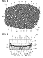
- FIG. 1 is an enlarged schematic sectional view of part of the phosphor layer 30.
- the phosphor layer 30 includes a plurality of phosphor particles 31 and a plurality of inorganic particles 32.
- the phosphor particle 31 is excited by emission light (excitation light) of the light emitting layer 13 and emits light of a wavelength different from the wavelength of the excitation light.
- emission light excitation light
- Light of white color or incandescent color is artificially obtained as mixed light of the light of the light emitting layer 13 and the light of the phosphor particles 31.
- the size of the inorganic particle 32 is smaller than the size of the phosphor particle 31.
- the size of a particle refers to the average particle diameter of a plurality of particles, or the peak particle diameter in the particle diameter distribution.
- a plurality of fine inorganic particles 32 are aggregated among the phosphor particles 31 and bind together the phosphor particles 31.
- One phosphor particle 31 is surrounded with the inorganic particles 32.
- the phosphor particles 31 and the inorganic particles 32 are aggregated and brought into contact with each other without the intermediary of resin. Thus, the phosphor particles 31 are bound together.
- the inorganic particles 32 are aggregated and brought into contact with each other without the intermediary of resin. Thus, the inorganic particles 32 are bound together.
- the phosphor layer 30 of the embodiment is not a sintered body in which the phosphor particles 31 are bound by resin or inorganic binder. Instead, as described later, the phosphor layer 30 is an aggregate of the phosphor particles 31 and the inorganic particles 32. The aggregate is formed by aerosol deposition technique or volatilization of a solvent. The phosphor layer 30 includes no resin. The layer of the aggregate of the phosphor particles 31 and the inorganic particles 32 is formed.
- Voids 33 are formed among the inorganic particles 32, and between the inorganic particles 32 and the phosphor particles 31.
- the inorganic particles 32 functioning as binder for binding together the phosphor particles 31 is not a sintered body. Thus, a grain boundary exists among the inorganic particles 32.
- the inorganic particle 32 is transmissive to emission light of the light emitting layer 13 and emission light of the phosphor particles 31.
- the term "transmissive” is not limited to a transmittance of 100%, but also includes the case of partially absorbing light.
- the inorganic particle 32 has a higher thermal conductivity than resin and silicon oxide.
- the thermal conductivity of the inorganic particle 32 is 20 W/m ⁇ K or more.
- the inorganic particle 32 can be composed primarily of aluminum oxide (Al 2 O 3 ), silicon nitride (Si 3 N 4 ), or silicon carbide (SiC).
- the phosphor particle 31 emitting light generates heat by the amount of wavelength conversion loss (Stokes loss).
- the resin may deteriorate or decompose by the heat of the phosphor particles 31. Heat resistance of resin may become a problem particularly in high-power light emitting elements.
- the phosphor layer 30 does not use resin as binder. This can improve the heat resistance of the phosphor layer 30. Furthermore, heat of the phosphor particles 31 can be dissipated to the outside of the phosphor layer 30 by the inorganic particles 32 having high thermal conductivity. For instance, heat of the phosphor particles 31 is dissipated to the mounting substrate through the light emitting element 4 and the metal pillars 23, 24 of the support body 100 shown in FIG. 2 .
- the phosphor layer 30 is not laminated with the light emitting element 4 via a resin adhesive (resin film). There is no resin in the heat dissipation path between the phosphor layer 30 and the light emitting element 4. This enhances the heat dissipation capability of the phosphor layer 30. Furthermore, there is no problem of resin degradation due to heat of the phosphor layer 30.
- the inorganic particles 32 having higher Young's modulus than resin are used as binder. This can reduce the coefficient of thermal expansion of the phosphor layer 30. Thus, the stress applied from the phosphor layer 30 to the semiconductor layer 15 can be relaxed. This enhances the reliability of the semiconductor layer 15.
- the embodiment can provide a semiconductor light emitting device being superior in heat dissipation capability of the phosphor layer 30 and having high reliability.
- the phosphor particle 31 can be made of e.g. an oxide-based phosphor such as Y 3 Al 5 O 12 , Ba 2 SiO 4 :Eu 2+ , and SrBaSiO 4 :Eu 2+ , a sulfide-based phosphor such as ZnS:(Cu + ,Al 3+ ), SrS:Eu 2+ , CaS:Eu 2+ , and SrGa 2 S 4 :Eu 2+ , an oxysulfide-based phosphor such as Y 2 O 2 S:Eu 3+ , a halide-based phosphor such as M 5 (PO 4 ) 3 Cl:Eu 2+ (M being Sr, Ca, Ba, or Mg), or an aluminate-based phosphor such as BaMgAl 10 O 17 :(Eu 2+ ,Mn 2+ ) and SrAl 2 O 4 :Eu 2+ .
- the phosphor particle 31 can be made of e.g. calcium magnesium chlorosilicate doped with Eu represented by the chemical formula Ca 8-x Eu x Mg 1-y Mn y (SiO 4 ) 4 Cl 2 (0 ⁇ x ⁇ 8, 0 ⁇ y ⁇ 1).
- the ratio y of manganese (Mn) is preferably 0 ⁇ y ⁇ 0.2.
- the phosphor particle 31 can be made of e.g. a strontium silicate-based phosphor represented by the chemical formula (Sr 1-x-y Ba y Eu x ) 3 (Si 1-z Ge z ) 5 (0 ⁇ x ⁇ 0.1, 0 ⁇ y ⁇ 1, 0 ⁇ z ⁇ 0.1).
- the phosphor particle 31 can be made of e.g. a sialon-based phosphor represented by the chemical formula (M 1-x ,R x ) a1 AlSi b1 O c1 N d1 .
- M is at least one metallic element except Si and Al, and preferably at least one of Ca and Sr.
- R is an emission center element, and preferably Eu.
- the values x, a1, b1, c1, and d1 satisfy the following relations. 0 ⁇ x ⁇ 1 , 0.6 ⁇ a 1 ⁇ 0.95 , 2 ⁇ b 1 ⁇ 3.9 , 0.25 ⁇ c 1 ⁇ 0.45 , 4 ⁇ d 1 ⁇ 5.7 ,
- the phosphor particle 31 can be made of e.g. a sialon-based phosphor represented by the chemical formula (M 1-x ,R x ) a2 AlSi b2 O c2 N d2 .
- M is at least one metallic element except Si and Al, and preferably at least one of Ca and Sr.
- R is an emission center element, and preferably Eu.
- the values x, a2, b2, c2, and d2 satisfy the following relations. 0 ⁇ x ⁇ 1 , 0.93 ⁇ a 2 ⁇ 1.3 , 4.0 ⁇ b 2 ⁇ 5.8 , 0.6 ⁇ c 2 ⁇ 1 , 6 ⁇ d 2 ⁇ 11
- the phosphor particle 31 is not limited to being made of a single phosphor material, but may be made of a mixture of a plurality of kinds of phosphor materials, including phosphor materials other than the aforementioned phosphor materials.
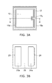
- FIG. 3A is a schematic plan view showing an example of the planar layout of some components in the semiconductor light emitting device 101.
- FIG. 2 corresponds to A-A' cross section in FIG. 3A .
- FIG. 3B is a schematic plan view of the mounting surface (the lower surface in FIG. 2 ) of the semiconductor light emitting device 101.
- the semiconductor layer 15 includes a first layer 11, a second layer 12, and a light emitting layer 13 provided between the first layer 11 and the second layer 12.
- the first layer 11 has a first surface (asperity surface) 15a.
- the semiconductor layer 15 includes a portion 15d and a portion 15e.
- the portion 15d includes a stacked film of the light emitting layer 13 and the second layer 12.
- the portion 15e does not include the light emitting layer 13 and the second layer 12.
- the portion 15d is a portion of the semiconductor layer 15 in which the light emitting layer 13 is stacked.
- the portion 15e is a portion of the semiconductor layer 15 in which the light emitting layer 13 is not stacked.
- a p-side electrode 16 is provided on the surface of the second layer 12 of the portion 15d including the light emitting layer 13.
- An n-side electrode 17 is provided on the surface of the first layer 11 of the portion 15e not including the light emitting layer 13.
- the p-side electrode 16 and the n-side electrode 17 are provided on the opposite side from the first surface 15a.
- the portion 15e not including the light emitting layer 13 surrounds the portion 15d including the light emitting layer 13.
- the n-side electrode 17 surrounds the p-side electrode 16.
- the area of the portion 15d including the light emitting layer 13 is larger than the area of the portion 15e not including the light emitting layer 13.
- the area of the p-side electrode 16 provided on the surface of the portion 15d including the light emitting layer 13 is larger than the area of the n-side electrode 17 provided on the surface of the portion 15e not including the light emitting layer 13.
- the n-side electrode 17 includes e.g. four linear parts. Among them, one linear part includes a contact part 17c projected in the width direction of the linear part. A via 22a of the n-side wiring layer 22 is connected to the surface of the contact part 17c as shown in FIG. 2 .
- a support body 100 is provided on the opposite side of the semiconductor layer 15 from the first surface 15a.
- the light emitting element 4 including the semiconductor layer 15, the p-side electrode 16, and the n-side electrode 17 is supported by the support body 100.
- the aforementioned phosphor layer 30 is provided on the first surface 15a side of the semiconductor layer 15.
- a transparent inorganic film 19 is provided between the first surface 15a of the semiconductor layer 15 and the phosphor layer 30.
- the transparent inorganic film 19 enhances adhesiveness between the semiconductor layer 15 and the phosphor layer 30.
- the opposite side (second surface side) of the semiconductor layer 15 from the first surface 15a, the p-side electrode 16, and the n-side electrode 17 are covered with an insulating film 18.
- the insulating film 18 is e.g. an inorganic insulating film such as silicon oxide film.
- the insulating film 18 is provided also on the side surface of the light emitting layer 13 and the side surface of the second layer 12.
- the insulating film 18 covers the side surface of the light emitting layer 13 and the side surface of the second layer 12.
- the insulating film 18 is provided also on the side surface 15c of the first layer 11 continued from the first surface 15a.
- the insulating film 18 covers the side surface 15c.
- a p-side wiring layer 21 and an n-side wiring layer 22 are provided on the insulating film 18 and separated from each other.
- a plurality of first openings communicating with the p-side electrode 16 and a second opening communicating with the contact part 17c of the n-side electrode 17 are formed in the insulating film 18.
- the first openings may be one larger opening.
- the p-side wiring layer 21 is provided on the insulating film 18 and inside the first opening.
- the p-side wiring layer 21 is electrically connected to the p-side electrode 16 through a via 21a provided in the first opening.
- the n-side wiring layer 22 is provided on the insulating film 18 and inside the second opening.
- the n-side wiring layer 22 is electrically connected to the contact part 17c of the n-side electrode 17 through a via 22a provided in the second opening.
- the p-side wiring layer 21 and the n-side wiring layer 22 occupy a large proportion of the second surface side of the semiconductor layer 15 and spread on the insulating film 18.
- the p-side wiring layer 21 is connected to the p-side electrode 16 through a plurality of vias 21a.
- a reflective film 51 covers the side surface 15c of the semiconductor layer 15 via the insulating film 18.
- the reflective film 51 is not in contact with the side surface 15c.
- the reflective film 51 is not electrically connected to the semiconductor layer 15.
- the reflective film 51 is separated from the p-side wiring layer 21 and the n-side wiring layer 22.
- the reflective film 51 is a metal film reflective to emission light of the light emitting layer 13 and emission light of the phosphor 31.
- the reflective film 51, the p-side wiring layer 21, and the n-side wiring layer 22 are simultaneously formed on a common metal film by e.g. plating technique.
- the reflective film 51, the p-side wiring layer 21, and the n-side wiring layer 22 include e.g. a copper film.
- the copper film is formed by plating technique on the metal film formed on the insulating film 18.
- the metal film underlying the p-side wiring layer 21 and the n-side wiring layer 22 includes e.g. an aluminum film.
- the aluminum film has high reflectance to emission light of the light emitting layer 13.
- the aluminum film is formed over a large proportion of the second surface side of the semiconductor layer 15. This can increase the amount of light directed to the phosphor layer 30 side.
- a p-side metal pillar 23 is provided on the surface of the p-side wiring layer 21 on the opposite side from the semiconductor layer 15.
- a p-side wiring section 41 includes the p-side wiring layer 21 and the p-side metal pillar 23.
- An n-side metal pillar 24 is provided on the surface of the n-side wiring layer 22 on the opposite side from the semiconductor layer 15.
- An n-side wiring section 43 includes the n-side wiring layer 22 and the n-side metal pillar 24.
- a resin layer 25 is provided as an insulating layer between the p-side wiring section 41 and the n-side wiring section 43.
- the resin layer 25 is provided on the side surface of the p-side wiring section 41 and the side surface of the n-side wiring section 43.
- the resin layer 25 is provided between the p-side metal pillar 23 and the n-side metal pillar 24 so as to be in contact with the side surface of the p-side metal pillar 23 and the side surface of the n-side metal pillar 24.
- the resin layer 25 is filled between the p-side metal pillar 23 and the n-side metal pillar 24.
- the resin layer 25 is provided between the p-side wiring layer 21 and the n-side wiring layer 22, between the p-side wiring layer 21 and the reflective film 51, and between the n-side wiring layer 22 and the reflective film 51.
- the resin layer 25 is provided around the p-side metal pillar 23 and around the n-side metal pillar 24.
- the resin layer 25 covers the side surface of the p-side metal pillar 23 and the side surface of the n-side metal pillar 24.
- the resin layer 25 is provided also in the region (chip outer peripheral part) adjacent to the side surface 15c of the semiconductor layer 15.
- the resin layer 25 covers the reflective film 51.
- the end part (surface) of the p-side metal pillar 23 on the opposite side from the p-side wiring layer 21 is exposed from the resin layer 25.
- the end part functions as a p-side external terminal 23a connectable to an external circuit of e.g. the mounting substrate.
- the end part (surface) of the n-side metal pillar 24 on the opposite side from the n-side wiring layer 22 is exposed from the resin layer 25.
- the end part functions as an n-side external terminal 24a connectable to an external circuit of e.g. the mounting substrate.
- the p-side external terminal 23a and the n-side external terminal 24a are bonded to pads of the mounting substrate through e.g. solder or a conductive bonding material.
- the p-side external terminal 23a and the n-side external terminal 24a are juxtaposed and spaced from each other in the same surface (lower surface) of the resin layer 25.
- the p-side external terminal 23a is formed in e.g. a rectangular shape.
- the n-side external terminal 24a is formed in a rectangular shape of the same size as the rectangle of the p-side external terminal 23a except that two corners are chamfered. This enables determination of the polarity of the external terminals.
- the n-side external terminal 24a may be shaped like a rectangle
- the p-side external terminal 23a may be shaped like a rectangle with chamfered corners.
- the spacing between the p-side external terminal 23a and the n-side external terminal 24a is wider than the spacing between the p-side wiring layer 21 and the n-side wiring layer 22 on the insulating film 18.
- the spacing between the p-side external terminal 23a and the n-side external terminal 24a is made larger than the spread of solder at the time of mounting. This can prevent short circuit between the p-side external terminal 23a and the n-side external terminal 24a through solder.
- the spacing between the p-side wiring layer 21 and the n-side wiring layer 22 can be narrowed to the process limit. This can expand the area of the p-side wiring layer 21, and the contact area between the p-side wiring layer 21 and the p-side metal pillar 23. Thus, heat dissipation of the light emitting layer 13 can be facilitated.
- the area of the p-side wiring layer 21 in contact with the p-side electrode 16 through a plurality of vias 21a is larger than the area of the n-side wiring layer 22 in contact with the n-side electrode 17 through the via 22a.
- the distribution of current flowing in the light emitting layer 13 can be made uniform.
- the area of the n-side wiring layer 22 spread on the insulating film 18 can be made larger than the area of the n-side electrode 17.
- the area of the n-side metal pillar 24 provided on the n-side wiring layer 22 (the area of the n-side external terminal 24a) can be made larger than that of the n-side electrode 17. This can reduce the area of the n-side electrode 17 while ensuring the area of the n-side external terminal 24a sufficient for mounting with high reliability. That is, optical output can be improved by reducing the area of the portion 15e of the semiconductor layer 15 not including the light emitting layer 13 and expanding the area of the portion 15d including the light emitting layer 13.
- the first layer 11 is electrically connected to the n-side metal pillar 24 through the n-side electrode 17 and the n-side wiring layer 22.
- the second layer 12 is electrically connected to the p-side metal pillar 23 through the p-side electrode 16 and the p-side wiring layer 21.
- the thickness of the p-side metal pillar 23 (the thickness in the direction connecting the p-side wiring layer 21 and the p-side external terminal 23a) is thicker than the thickness of the p-side wiring layer 21.
- the thickness of the n-side metal pillar 24 (the thickness in the direction connecting the n-side wiring layer 22 and the n-side external terminal 24a) is thicker than the thickness of the n-side wiring layer 22.
- Each thickness of the p-side metal pillar 23, the n-side metal pillar 24, and the resin layer 25 is thicker than that of the semiconductor layer 15.
- the aspect ratio (ratio of thickness to planar size) of the metal pillar 23, 24 may be 1 or more, or smaller than 1. That is, the metal pillar 23, 24 may be thicker or thinner than the planar size thereof.
- the thickness of the support body 100 including the p-side wiring layer 21, the n-side wiring layer 22, the p-side metal pillar 23, the n-side metal pillar 24, and the resin layer 25 is thicker than the thickness of the light emitting element (LED chip) 4 including the semiconductor layer 15, the p-side electrode 16, and the n-side electrode 17.
- the semiconductor layer 15 is formed on the substrate by epitaxial growth technique.
- the substrate is removed after the support body 100 is formed.
- the semiconductor layer 15 does not include the substrate on the first surface 15a side.
- the semiconductor layer 15 is supported not by a rigid plate-like substrate, but by the support body 100 made of a composite of the metal pillars 23, 24 and the resin layer 25.
- the material of the p-side wiring section 41 and the n-side wiring section 43 can be e.g. copper, gold, nickel, or silver. Among them, copper can achieve good thermal conductivity, high migration resistance, and good adhesiveness to insulating material.
- the resin layer 25 reinforces the p-side metal pillar 23 and the n-side metal pillar 24.
- the resin layer 25 is preferably made of a material having a thermal expansion rate equal or close to that of the semiconductor layer 15.
- Such a resin layer 25 can be made of a composite material in which e.g. silica filler is mixed in a resin primarily containing epoxy resin, a resin primarily containing silicone resin, or a resin primarily containing fluororesin.
- the base resin of the resin layer 25 may include e.g. a light-absorbing agent, a light-reflecting agent, or a light-scattering agent.
- the resin layer 25 can have light blocking capability or reflectivity to light of the light emitting layer 13. This can suppress light leakage from the side surface and the mounting surface side of the support body 100.
- the semiconductor layer 15 is subjected to stress due to e.g. solder for bonding the p-side external terminal 23a and the n-side external terminal 24a to the pads of the mounting substrate.
- the p-side metal pillar 23, the n-side metal pillar 24, and the resin layer 25 absorb and relax the stress.
- the resin layer 25 softer than the semiconductor layer 15 is used as part of the support body 100. This can enhance the stress relaxation effect.
- the reflective film 51 is separated from the p-side wiring section 41 and the n-side wiring section 43.
- the stress applied to the p-side metal pillar 23 and the n-side metal pillar 24 at the time of mounting is not transmitted to the reflective film 51.
- This can suppress peeling of the reflective film 51.
- this can suppress stress applied to the side surface 15c side of the semiconductor layer 15.
- the phosphor layer 30 is not formed on the second surface side of the semiconductor layer 15, around the metal pillars 23, 24, and on the side surface of the support body 100.
- the side surface of the phosphor layer 30 is aligned with the side surface of the support body 100 (the side surface of the resin layer 25).
- the side surface of the phosphor layer 30 and the side surface of the support body 100 (the side surface of the resin layer 25) are continuous on the same plane.
- the semiconductor light emitting device 101 shown in FIG. 2 is a semiconductor light emitting device of the chip-size package structure having a very small size.
- the semiconductor light emitting device 101 is superior in heat dissipation capability in spite of its small size.
- an LED chip is mounted on the mounting substrate via e.g. bumps. Then, a phosphor layer is formed so as to entirely cover the chip. Alternatively, resin is underfilled between the bumps.
- the resin layer 25 different from the phosphor layer 30 is provided around the p-side metal pillar 23 and around the n-side metal pillar 24 before mounting. This can provide the mounting surface side with characteristics suitable for stress relaxation. Furthermore, the resin layer 25 already provided on the mounting surface side dispenses with underfilling after mounting.
- the phosphor layer 30 designed preferentially for light extraction efficiency, color conversion efficiency, and light distribution characteristics is provided on the first surface 15a side.
- Layers designed preferentially for stress relaxation at the time of mounting and characteristics for a support body replacing the substrate are provided on the mounting surface side.
- the resin layer 25 can be filled with a filler such as silica particles at high density.
- the hardness of the resin layer 25 can be adjusted to a level suitable for a support body.
- Light emitted from the light emitting layer 13 to the first surface 15a side is incident on the phosphor layer 30. Part of the light excites the phosphor particles 31. For instance, white light is artificially obtained as mixed light of the light of the light emitting layer 13 and the light of the phosphor particles 31.
- part of the light fails to be incident on the phosphor layer 30 and leaks outside from the side surface of the substrate. That is, light of a strong color of the light emitting layer 13 leaks from the side surface of the substrate. This may cause color breakup or color unevenness such as a phenomenon in which a ring of blue light appears on the outer edge side of the phosphor layer 30 as viewed from above the upper surface.
- the embodiment there is no substrate between the first surface 15a and the phosphor layer 30. This can prevent color breakup or color unevenness caused by leakage of light of a strong color of the light emitting layer 13 from the substrate side surface.
- the reflective film 51 is provided on the side surface 15c of the first layer 11 via the insulating film 18. Light directed from the light emitting layer 13 toward the side surface 15c of the first layer 11 is reflected by the reflective film 51, and does not leak outside. This can prevent color breakup or color unevenness caused by light leakage from the side surface side of the semiconductor light emitting device 101 in combination with the absence of a substrate on the first surface 15a side.
- the insulating film 18 is provided between the reflective film 51 and the side surface 15c of the first layer 11.
- the insulating film 18 prevents diffusion of the metal contained in the reflective film 51 to the first layer 11. This can prevent metal contamination of e.g. GaN contained in the first layer 11. Thus, degradation of the first layer 11 can be prevented.
- the phosphor layer 30 can be formed by e.g. aerosol deposition technique.
- FIG. 8 is a schematic view of an example of an aerosol deposition apparatus.
- a support body 100 including metal pillars 23, 24 and a resin layer 25 is formed in the wafer state including a plurality of light emitting elements 4. Then, the substrate used for growth of the semiconductor layer 15 is removed. After the substrate is removed, the wafer 209 is set in a deposition chamber 207. The wafer 209 is held by a stage 212 provided outside the deposition chamber 207. The deposition chamber 207 is connected to a vacuum pump 211 through an exhaust pipe 210 and filled with a reduced-pressure atmosphere having a lower pressure than the aerosol chamber 203.
- Phosphor particles 31 and inorganic particles 32 are mixed into source particles 204.
- the source particles 204 are set in the aerosol chamber 203.
- a carrier gas such as helium, argon, and nitrogen is supplied from a high-pressure gas cylinder 201 through a gas supply pipe 202 into the aerosol chamber 203.
- the source particles 204 and the carrier gas are stirred and mixed into an aerosol by the aerosol generator 205.
- the aerosolized source particles 204 are transported with the carrier gas in a transport pipe 206.
- the source particles 204 are sprayed toward the wafer 209 from a nozzle 208 set in the deposition chamber 207.
- the aerosolized source particles 204 are sprayed toward the first surface 15a of the semiconductor layer 15 or the transparent inorganic film 19 formed on the first surface 15a in the wafer 209.
- the kinetic energy of the aerosolized source particles 204 is converted to the energy for binding particles on the wafer 209 and the energy for attaching the particles to the wafer.
- an aggregate of a plurality of phosphor particles 31 and a plurality of inorganic particles 32 is formed like a layer on the first surface 15a.
- the embodiment is not limited to the case where phosphor particles 31 and inorganic particles 32 are mixed and sprayed to the wafer 209. Phosphor particles 31 and inorganic particles 32 may be separately sprayed to form an aggregate on the wafer 209.
- the aerosol deposition technique can bombard and attach source particles to the wafer in the solid state at normal temperature.
- An alternative method for forming the phosphor layer 30 is to utilize volatilization of a solvent.
- a plurality of phosphor particles 31 and a plurality of inorganic particles 32 are dispersed in a low-viscosity solvent to form a solution (slurry).
- the solution is supplied onto the wafer by e.g. spin coating technique, printing technique, or dispensing technique. Then, the solvent is volatilized to form an aggregate of a plurality of phosphor particles 31 and a plurality of inorganic particles 32 on the wafer.
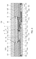
- FIG. 4 is a schematic sectional view of a semiconductor light emitting device 102 of a second embodiment.
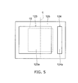
- FIG. 5 is a schematic plan view of the mounting surface side of the semiconductor light emitting device 102.
- FIG. 5 corresponds to a bottom view of FIG. 4 .
- the semiconductor light emitting device 102 includes a chip-size light emitting element (LED chip) 5 formed in the wafer level, an insulating member 127 provided around the light emitting element 5, and metal layers 171, 172 provided on the mounting surface side.
- LED chip chip-size light emitting element
- the light emitting element 5 includes electrodes 7, 8, first wiring layers (on-chip wiring layers) 116, 117, optical layers 30, 133, and a semiconductor layer 15 provided between the first wiring layer 116, 117 and the optical layer 30, 133.
- FIG. 6 is an enlarged schematic sectional view of the semiconductor layer 15.
- the semiconductor layer 15 includes a first layer 11, a second layer 12, and a light emitting layer 13 provided between the first layer 11 and the second layer 12.
- the semiconductor layer 15 includes a first portion 15d and a second portion 15e.
- the first portion 15d includes a stacked film of the second layer 12 and the light emitting layer 13.
- the second portion 15e has a second surface 11a of the first layer 11 not covered with the light emitting layer 13 and the second layer 12.
- the second portion 15e is formed like an island surrounded with the first portion 15d. Furthermore, the second portion 15e is formed so as to continuously surround the first portion 15d on the outer peripheral side of the first portion 15d.
- the area of the first portion 15d including the light emitting layer 13 is larger than the area of the second portion 15e not including the light emitting layer 13.
- a first surface (asperity surface) 15a is formed on the opposite side of the first layer 11 from the second surface 11a.
- the first surface 15a is not covered with the light emitting layer 13 and the second layer 12.
- the semiconductor layer 15 has a side surface 15c continued to the first surface 15a.
- the n-side electrode 8 shown in FIG. 4 is provided on the second surface 11a of the first layer 11.
- the p-side electrode 7 shown in FIG. 4 is provided on the surface of the second layer 12.
- the p-side electrode 7 and the n-side electrode 8 are formed within the region (chip region) overlapping the semiconductor layer 15.
- the area of the p-side electrode 7 is larger than the area of the n-side electrode 8.
- the contact area between the p-side electrode 7 and the second layer 12 is larger than the contact area between the n-side electrode 8 and the first layer 11.
- An insulating film 114 is provided on the surface of the semiconductor layer 15 other than the first surface 15a.
- the insulating film 114 is an inorganic film such as silicon oxide film.
- a p-side opening communicating with the p-side electrode 7 and an n-side opening communicating with the n-side electrode 8 are formed in the insulating film 114. For instance, two n-side openings are formed and spaced from each other. The surface of the p-side electrode 7 between the two n-side openings is covered with the insulating film 114.
- the side surface 15c of the first layer 11, the side surface of the second layer 12, and the side surface of the light emitting layer 13 are covered with the insulating film 114.
- a first p-side wiring layer 116 and a first n-side wiring layer 117 are provided on the opposite side of the semiconductor layer 15 from the first surface 15a.
- the first p-side wiring layer 116 is formed within the region (chip region) overlapping the semiconductor layer 15.
- the first p-side wiring layer 116 is provided also in the p-side opening and in contact with the p-side electrode 7.
- the first p-side wiring layer 116 is connected to the p-side electrode 7 through a contact part formed integrally therewith in the p-side opening.
- the first p-side wiring layer 116 is not in contact with the first layer 11.
- the first n-side wiring layer 117 is formed within the region (chip region) overlapping the semiconductor layer 15.
- the first n-side wiring layer 117 is provided also in the n-side opening and in contact with the n-side electrode 8.
- the first n-side wiring layer 117 is connected to the n-side electrode 8 through a contact part 117a formed integrally therewith in the n-side opening.
- the first n-side wiring layer 117 is formed in e.g. a line pattern extending in the direction connecting two island-shaped n-side electrodes 8.
- the insulating film 114 is provided between the p-side electrode 7 and the portion of the first n-side wiring layer 117 between the two n-side electrodes 8, and between the second layer 12 and the portion of the first n-side wiring layer 117 between the two n-side electrodes 8.
- the first n-side wiring layer 117 is not in contact with the p-side electrode 7 and the second layer 12.
- the p-side electrode 7 is provided between the second layer 12 and the first p-side wiring layer 116.
- the p-side electrode 7 includes a silver (Ag) film having high reflectance to light emitted by the light emitting layer 13 and the phosphor particles 31.
- the n-side electrode 8 is provided between the first layer 11 and the contact part 117a of the first n-side wiring layer 117.
- the n-side electrode 8 includes an aluminum (Al) film having high reflectance to light emitted by the light emitting layer 13 and the phosphor particles 31.
- An insulating film 118 is provided on the surface of the first p-side wiring layer 116 and the first n-side wiring layer 117.
- the insulating film 118 is provided also between first p-side wiring layer 116 and the first n-side wiring layer 117.
- the insulating film 118 is e.g. an inorganic film such as silicon oxide film.
- a p-side opening and an n-side opening are formed in the insulating film 118.
- the p-side opening exposes part (p-side pad 116b) of the first p-side wiring layer 116.
- the n-side opening exposes part (n-side pad 117b) of the first n-side wiring layer 117.
- the area of the p-side pad 116b is larger than the area of the n-side pad 117b.
- the area of the n-side pad 117b is larger than the contact area between the first n-side wiring layer 117 and the n-side electrode 8.
- a phosphor layer 30 is provided on the first surface 15a side of the semiconductor layer 15. Furthermore, a transparent layer (first transparent layer) 133 is provided on the phosphor layer 30. As described above, the phosphor layer 30 is an aggregate of a plurality of phosphor particles 31 and a plurality of inorganic particles 32.
- a transparent inorganic film 19 is provided between the first surface 15a and the phosphor layer 30.
- the transparent inorganic film 19 and the phosphor layer 30 are provided also on the insulating film 114 in the off-chip region.
- the transparent layer 133 on the phosphor layer 30 is made of transparent glass or transparent resin not including phosphor particles.
- the transparent layer 133 may be caused to function as a light-scattering layer.
- the transparent layer 133 includes a plurality of particles of a scattering material (such as silicon oxide titanium compound, and zinc oxide), and a binding material (e.g., transparent resin or transparent glass).
- the scattering material scatters emission light of the light emitting layer 13.
- the binding material is transmissive to emission light of the light emitting layer 13.
- An insulating member 127 is provided in the off-chip region outside the side surface of the semiconductor layer 15.
- the insulating member 127 is thicker than the semiconductor layer 15.
- the insulating member 127 covers the side surface of the semiconductor layer 15 via the insulating film 114.
- the insulating member 127 is provided also outside the side surface of the optical layers (phosphor layer 30 and transparent layer 133).
- the insulating member 127 covers the side surface of the optical layers.
- the insulating member 127 is provided around the light emitting element 5 including the semiconductor layer 15, the electrodes 7, 8, the first wiring layers (on-chip wiring layers) 116, 117, and the phosphor layer 30.
- the insulating member 127 supports the light emitting element 5.
- the upper surface 127a of the insulating member 127 and the upper surface of the transparent layer 133 form a flat surface.
- An insulating film 126 is provided on the back surface of the insulating member 127.
- a second p-side wiring layer 121 is provided on the first p-side pad 116b of the first p-side wiring layer 116.
- the second p-side wiring layer 121 is in contact with the first p-side pad 116b of the first p-side wiring layer 116 and extends to the off-chip region.
- the portion of the second p-side wiring layer 121 extending to the off-chip region is supported by the insulating member 127 via the insulating film 126.
- Part of the second p-side wiring layer 121 extends also to the region overlapping the first n-side wiring layer 117 via the insulating film 118.
- a second n-side wiring layer 122 is provided on the first n-side pad 117b of the first n-side wiring layer 117.
- the second n-side wiring layer 122 is in contact with the first n-side pad 117b of the first n-side wiring layer 117 and extends to the off-chip region.
- the portion of the second n-side wiring layer 122 extending to the off-chip region is supported by the insulating member 127 via the insulating film 126.
- An insulating film 119 is provided on the surface of the second p-side wiring layer 121 and the second n-side wiring layer 122.
- the insulating film 119 is an inorganic film such as silicon oxide film.
- a p-side opening and an n-side opening are formed in the insulating film 119.
- the p-side opening exposes the second p-side pad 121a of the second p-side wiring layer 121.
- the n-side opening exposes the second n-side pad 122a of the second n-side wiring layer 122.
- a p-side external connection electrode 123 is provided on the second p-side pad 121a of the second p-side wiring layer 121.
- the p-side external connection electrode 123 is in contact with the second p-side pad 121a of the second p-side wiring layer 121 and provided on the second p-side wiring layer 121.
- Part of the p-side external connection electrode 123 is provided also on the region overlapping the first n-side wiring layer 117 via the insulating films 118, 119, and the region overlapping the second n-side wiring layer 122 via the insulating film 119.
- the p-side external connection electrode 123 spreads in the chip region overlapping the semiconductor layer 15, and the off-chip region.
- the p-side external connection electrode 123 is thicker than the first p-side wiring layer 116 and thicker than the second p-side wiring layer 121.
- An n-side external connection electrode 124 is provided on the second n-side pad 122a of the second n-side wiring layer 122.
- the n-side external connection electrode 124 is placed in the off-chip region and in contact with the second n-side pad 122a of the second n-side wiring layer 122.
- the n-side external connection electrode 124 is thicker than the first n-side wiring layer 117 and thicker than the second n-side wiring layer 122.
- a resin layer (insulating layer) 125 is provided between the p-side external connection electrode 123 and the n-side external connection electrode 124.
- the resin layer 125 is in contact with the side surface of the p-side external connection electrode 123 and the side surface of the n-side external connection electrode 124.
- the resin layer 125 is filled between the p-side external connection electrode 123 and the n-side external connection electrode 124.
- the resin layer 125 is provided around the p-side external connection electrode 123 and around the n-side external connection electrode 124.
- the resin layer 125 covers the side surface of the p-side external connection electrode 123 and the side surface of the n-side external connection electrode 124.
- the resin layer 125 enhances the mechanical strength of the p-side external connection electrode 123 and the n-side external connection electrode 124.
- the resin layer 125 functions as a solder resist for preventing wetting and spreading of solder at the time of mounting.
- the lower surface of the p-side external connection electrode 123 is exposed from the resin layer 125 and functions as a p-side mounting surface (p-side external terminal) 123a connectable to an external circuit of e.g. the mounting substrate.
- the lower surface of the n-side external connection electrode 124 is exposed from the resin layer 125 and functions as an n-side mounting surface (n-side external terminal) 124a connectable to an external circuit of e.g. the mounting substrate.
- the p-side mounting surface 123a and the n-side mounting surface 124a are bonded to a land pattern of the mounting substrate through e.g. solder or a conductive bonding material.
- the p-side mounting surface 123a and the n-side mounting surface 124a are preferably projected from the surface of the resin layer 125. This stabilizes the solder shape of the connection part at the time of mounting. Thus, the reliability of mounting can be improved.
- FIG. 5 shows an example of the planar layout of the p-side mounting surface 123a and the n-side mounting surface 124a.
- the p-side mounting surface 123a and the n-side mounting surface 124a are placed asymmetrically with respect to the center line c bisecting the planar region of the semiconductor layer 15.
- the p-side mounting surface 123a is larger than the n-side mounting surface 124a.
- the spacing between the p-side mounting surface 123a and the n-side mounting surface 124a is set so that solder does not bridge the gap between the p-side mounting surface 123a and the n-side mounting surface 124a at the time of mounting.
- the n-side electrode contact surface (the second surface 11a of the first layer 11) in the semiconductor layer 15 is relocated in a larger region including the off-chip region by the first n-side wiring layer 117 and the second n-side wiring layer 122.
- This can reduce the area of the n-side electrode surface in the semiconductor layer 15 while ensuring the area of the n-side mounting surface 124a sufficient for mounting with high reliability.
- the area of the portion 15e not including the light emitting layer 13 in the semiconductor layer 15 can be reduced, and the area of the portion 15d including the light emitting layer 13 can be expanded. This can improve the optical output.
- a p-side metal layer 171 and an n-side metal layer 172 are provided on the mounting surface side.
- the p-side metal layer 171 includes the first p-side wiring layer 116, the second p-side wiring layer 121, and the p-side external connection electrode 123.
- the n-side metal layer 172 includes the first n-side wiring layer 117, the second n-side wiring layer 122, and the n-side external connection electrode 124.
- the semiconductor layer 15 is supported on the support body made of a composite of the metal layers 171, 172 and the resin layer 125.
- the semiconductor layer 15 is supported from the side surface side by the insulating member 127.
- the insulating member 127 is e.g. a resin layer thicker than the semiconductor layer 15.
- the material of the metal layers 171, 172 can be e.g. copper, gold, nickel, or silver. Among them, copper can achieve good thermal conductivity, high migration resistance, and good adhesiveness to insulating material.
- the semiconductor layer 15 is subjected to stress due to e.g. solder for bonding the p-side mounting surface 123a and the n-side mounting surface 124a to the lands of the mounting substrate.
- the p-side external connection electrode 123, the n-side external connection electrode 124, and the resin layer 125 may be formed with a suitable thickness (height). Then, the p-side external connection electrode 123, the n-side external connection electrode 124, and the resin layer 125 can absorb and relax the aforementioned stress.
- the resin layer 125 softer than the semiconductor layer 15 is used as part of the support body on the mounting surface side. This can enhance the stress relaxation effect.
- the metal layers 171, 172 are composed primarily of e.g. copper having high thermal conductivity. Thus, a high thermal conductor spreads in a large area on the region overlapping the light emitting layer 13. Heat generated in the light emitting layer 13 is dissipated to the mounting substrate by a short path formed below the chip through the metal layers 171, 172.
- the p-side mounting surface 123a of the p-side metal layer 171 connected to the stacked portion 15d including the light emitting layer 13 overlaps most of the planar region of the semiconductor layer 15 in plan view shown in FIG. 5 .
- heat can be dissipated with high efficiency to the mounting substrate through the p-side metal layer 171.
- the p-side mounting surface 123a is extended also to the off-chip region. This can enlarge the planar size of the solder bonded to the p-side mounting surface 123a. Thus, heat dissipation to the mounting substrate through the solder can be improved.
- the second n-side wiring layer 122 extends to the off-chip region.
- the n-side mounting surface 124a can be placed in the off-chip region without the constraint of the p-side mounting surface 123a laid out over a large proportion of the region overlapping the chip.
- the area of the n-side mounting surface 124a can be made larger than that in the case where the n-side mounting surface 124a is laid out only within the chip region.
- the planar size of the solder bonded to the n-side mounting surface 124a can be made larger to improve heat dissipation to the mounting substrate through the solder.
- Light emitted from the light emitting layer 13 to the first surface 15a side is incident on the phosphor layer 30 through the transparent inorganic film 19. Part of the light excites the phosphor 31. For instance, white light is obtained as mixed light of the light of the light emitting layer 13 and the light of the phosphor particles 31.
- Light emitted from the light emitting layer 13 to the mounting surface side is reflected by the p-side electrode 7 and the n-side electrode 8 and directed toward the phosphor layer 30 thereabove.
- a transparent layer (first transparent layer) 133 is provided on the phosphor layer 30.
- a transparent layer (second transparent layer) 134 is provided on the transparent layer 133 and on the insulating member 127 in the off-chip region.
- the transparent layer 134 is made of transparent glass or transparent resin.
- an adhesive layer made of transparent resin may be inserted.
- the transparent layer 134 may include a plurality of particles of a scattering material (such as silicon oxide titanium compound, and zinc oxide), and a binding material (e.g., transparent resin or transparent glass).
- the scattering material scatters emission light of the light emitting layer 13.
- the binding material is transmissive to emission light of the light emitting layer 13.
- the transparent layer 134 functions as a light scattering layer.
- the planar size of the transparent layer 134 functioning as a light scattering layer is larger than the planar size of the phosphor layer 30 and the planar size of the transparent layer 133. That is, the planar size of the transparent layer 134 is larger than the planar size of the light emitting element 5. This can expand the range of light emitted outside from the semiconductor light emitting device 102 and enables wide-angle light distribution characteristics.
- the surface of at least the portion of the insulating member 127 close to the side surface of the semiconductor layer 15 is reflective to emission light of the light emitting layer 13.
- the portion of the insulating member 127 close to the side surface of the phosphor layer 30 and close to the side surface of the transparent layer 133 is reflective to emission light of the light emitting layer 13 and emission light of the phosphor particles 31.
- the insulating member 127 near the boundary with the transparent layer 134 is reflective to emission light of the light emitting layer 13 and emission light of the phosphor particles 31.
- the insulating member 127 is a resin layer having a reflectance of 50% or more to emission light of the light emitting layer 13 and emission light of the phosphor particles 31.
- emission light from the side surface of the light emitting element 5 and light scattered by the transparent layer 134 and directed to the insulating member 127 side can be reflected by the insulating member 127. This can prevent absorption loss of light in the insulating member 127 to enhance the efficiency of light extraction to the outside through the transparent layer 134.
- the phosphor layer 30 is not formed on the side surface of the semiconductor layer 15 and on the mounting surface side. That is, the phosphor layer 30 is not formed uselessly on the chip side surface side and the mounting surface side from which light is not extracted outside. This can reduce the cost.
- the resin layer 125 different from the phosphor layer 30 is provided around the p-side external connection electrode 123 and around the n-side external connection electrode 124. This can provide the mounting surface side with characteristics suitable for stress relaxation. Furthermore, the resin layer 125 already provided on the mounting surface side dispenses with underfilling after mounting the semiconductor light emitting device 102 on the mounting substrate.
- the phosphor layer 30 designed preferentially for light extraction efficiency, color conversion efficiency, and light distribution characteristics is provided on the first surface 15a side of the semiconductor layer 15.
- Layers designed preferentially for stress relaxation at the time of mounting and characteristics for a support body replacing the substrate are provided on the mounting surface side.
- the resin layer 125 has a structure in which a base resin is filled with filler such as silica particles at high density. Thus, the hardness of the resin layer 125 is adjusted to a level suitable for a support body.
- the semiconductor layer 15, the electrodes 7, 8, the on-chip wiring layers 116, 117, and the phosphor layer 30 are collectively formed in the wafer level. This realizes a chip-size light emitting element 5 at low cost. Furthermore, the external terminals (mounting surfaces) 123a, 124a can be extended to the off-chip region to improve heat dissipation capability. Thus, a semiconductor light emitting device 102 with high reliability can be provided at low cost.
- FIG. 7 is a schematic sectional view of a semiconductor light emitting device 103 of a third embodiment.
- the semiconductor light emitting device 103 includes a support substrate 10, a phosphor layer 30, and a semiconductor layer 15 provided between the support substrate 10 and the phosphor layer 30.
- the semiconductor layer 15 includes a first layer 11, a second layer 12, and a light emitting layer 13 provided between the first layer 11 and the second layer 12.
- the first layer 11 has a first surface (asperity surface) 15a.
- the support substrate 10 is provided on the opposite side of the semiconductor layer 15 from the first surface 15a via a metal layer (bonding metal) 63.
- a metal layer (back metal) 64 is provided on the surface of the support substrate 10 on the opposite side from the surface provided with the metal layer 63.
- the phosphor layer 30 is provided on the first surface 15a side of the semiconductor layer 15. As described above, the phosphor layer 30 is an aggregate of a plurality of phosphor particles 31 and a plurality of inorganic particles 32.
- a transparent inorganic film 19 is provided between the first surface 15a of the semiconductor layer 15 and the phosphor layer 30.
- a p-side electrode 61 is provided between the semiconductor layer 15 and the metal layer 63.
- the p-side electrode 61 is in contact with the second layer 12.
- Part of the p-side electrode 61 extends outside from the side surface of the semiconductor layer 15.
- a p-side pad 62 is provided on the extending part.
- the second layer 12 is electrically connected to the p-side pad 62 through the p-side electrode 61.
- An insulating film 65 is provided between the p-side electrode 61 and the metal layer 63.
- the p-side electrode 61 is insulated from the metal layer 63.
- a plurality of n-side electrodes 63a are provided on the metal layer 63 integrally with the metal layer 63.
- the n-side electrode 63a penetrates through the p-side electrode 61, the second layer 12, and the light emitting layer 13 to the first layer 11.
- the n-side electrode 63a is electrically connected to the first layer 11.
- An insulating film 65 is provided between the n-side electrode 63a and the light emitting layer 13, between the n-side electrode 63a and the second layer 12, and between the n-side electrode 63a and the p-side electrode 61.
- the semiconductor layer 15 is grown on the aforementioned monocrystalline substrate. After forming e.g. the p-side electrode 61 and the n-side electrodes 63a, the semiconductor layer 15 is laminated with the support substrate 10 via the metal layer 63.
- the support substrate 10 is conductive.
- the support substrate 10 is e.g. a silicon substrate.
- the first layer 11 is electrically connected to the metal layer (back surface electrode) 64 through the n-side electrode 63a, the metal layer 63, and the support substrate 10.
- the monocrystalline substrate is removed.
- the surface of the first layer 11 is exposed.
- the transparent inorganic film 19 is formed.
- the phosphor layer 30 is formed on the transparent inorganic film 19.
- a transparent inorganic film 34 covering the surface of the phosphor layer 30, i.e., the surface of the phosphor particles 31 and the surface of the inorganic particles 32, may be provided.
- a silicon oxide film is formed by sputtering technique, CVD (chemical vapor deposition) technique, or coating technique.
- the transparent inorganic film 34 protects the surface of the phosphor layer 30 and reinforces the binding between the particles.
- the gap between the inorganic particles 32, and the gap between the inorganic particles 32 and the phosphor particles 31, inside the surface of the phosphor particles 31 and the surface of the inorganic particles 32 can be impregnated with part of the transparent inorganic film 34.
- a silicon oxide film having low thermal conductivity may be formed as a transparent inorganic film 34. This can cause the transparent inorganic film 34 to function as a heat-insulating layer.
- the transparent inorganic film 34 may be formed between the phosphor layer 30 and the transparent resin layer 133 in the semiconductor light emitting device 102 shown in FIG. 4 . This can suppress alteration and decomposition of the transparent resin layer 133 by heat of the phosphor particles 31.
- a transparent resin 35 may be provided in the gap between the inorganic particles 32, and the gap between the inorganic particles 32 and the phosphor particles 31.
- the phosphor particles 31 and the inorganic particles 32 are not dispersed in the resin serving as a binder.
- an aggregate of phosphor particles 31 and inorganic particles 32 is formed by the aforementioned method. Then, the gap between the particles is impregnated with the transparent resin 35.
Landscapes
- Led Device Packages (AREA)
- Luminescent Compositions (AREA)
Abstract
Description
- Embodiments described herein relate generally to a semiconductor light emitting device and a method for forming a phosphor layer.
- In recent years, a semiconductor light emitting device realizing a white light source with a light emitting element of nitride semiconductor and a phosphor layer is widely used. In such a semiconductor light emitting device, particularly in the high-power type, there has been an increasing demand for countermeasures against heat generation not only in the light emitting element but also in the phosphor layer.
-
-
FIG. 1 is an enlarged schematic sectional view of part of a phosphor layer of an embodiment; -
FIG. 2 is a schematic sectional view of a semiconductor light emitting device of the embodiment; -
FIGS. 3A and 3B are schematic plan views showing the semiconductor light emitting device of the embodiment; -
FIG. 4 is a schematic sectional view of a semiconductor light emitting device of the embodiment; -
FIG. 5 is a schematic plan view of the semiconductor light emitting device of the embodiment; -
FIG. 6 is a schematic sectional view of a semiconductor layer of the embodiment; -
FIG. 7 is a schematic sectional view of a semiconductor light emitting device of the embodiment; -
FIG. 8 is a schematic view of an apparatus for forming the phosphor layer of the embodiment; -
FIG. 9 is an enlarged schematic sectional view of part of a phosphor layer of the embodiment; and -
FIG. 10 is an enlarged schematic sectional view of part of a phosphor layer of the embodiment. - According to one embodiment, a semiconductor light emitting device includes a light emitting element and a phosphor layer provided on the light emitting element. The phosphor layer includes a plurality of phosphor particles and a plurality of inorganic particles having smaller sizes than the phosphor particles. The phosphor particles are bound together with aggregation of the inorganic particles and the phosphor particles.
- Embodiments will now be described with reference to the drawings. In the drawings, like components are labeled with like reference numerals.
-
FIG. 2 is a schematic sectional view of a semiconductorlight emitting device 101 of a first embodiment. - The semiconductor
light emitting device 101 includes alight emitting element 4, asupport body 100, and aphosphor layer 30. Thelight emitting element 4 is provided between thesupport body 100 and thephosphor layer 30. - The
light emitting element 4 includes asemiconductor layer 15 containing nitride semiconductor. In this specification, the "nitride semiconductor" contains group III-V compound semiconductors of BxInyAlzGa1-x-y-zN (0≤x≤1, 0≤y≤1, 0≤z≤1, 0≤x+y+z≤1). The "nitride semiconductor" may be a mixed crystal containing other group V elements such as phosphorus (P) and arsenic (As) in addition to N (nitrogen). Furthermore, the "nitride semiconductor" may contain various elements added to control various material properties such as conductivity type, and various unintended elements. - The
semiconductor layer 15 includes afirst layer 11 including an n-type cladding layer, asecond layer 12 including a p-type cladding layer, and a light emitting layer (active layer) 13 provided between thefirst layer 11 and thesecond layer 12. - The n-type cladding layer is, for example, an n-type GaN layer. The n-type cladding layer supplies electrons to the
light emitting layer 13 under forward bias to the p-n junction. The p-type cladding layer is, for example, a p-type GaN layer. The p-type cladding layer supplies holes to thelight emitting layer 13 under forward bias to the p-n junction. - The
light emitting layer 13 has, for example, a multiple quantum well (MQW) structure in which a plurality of well layers and a plurality of barrier layers are alternately stacked. The well layer has lower bandgap energy than the n-type cladding layer and the p-type cladding layer. The well layer is interposed between the barrier layers in the stacking direction. The barrier layer has higher bandgap energy than the well layer. The well layer contains, for example, InGaN. The barrier layer contains, for example, GaN. The barrier layer does not substantially contain In. Alternatively, the barrier layer may contain In. In the case where the barrier layer contains In, the In composition ratio in the barrier layer is lower than the In composition ratio in the well layer. The range of the peak wavelength of light emitted from thelight emitting layer 13 is, for example, 360 nm or more and 650 nm or less. - The
phosphor layer 30 is provided on thefirst surface 15a side of thesemiconductor layer 15 via a transparentinorganic film 19. - The
semiconductor layer 15 is epitaxially grown on a monocrystalline substrate (hereinafter simply referred to as substrate) such as a silicon substrate, sapphire substrate, silicon carbide substrate, and gallium oxide substrate. Thefirst layer 11, thelight emitting layer 13, and thesecond layer 12 are sequentially formed on the substrate. The substrate used for formation (growth) of thesemiconductor layer 15 is removed from thesemiconductor layer 15. - Fine asperities are formed at the
first surface 15a of thefirst layer 11 exposed by the removal of the substrate. For example, an asperity surface is formed by wet etching with an alkali-based solution. This asperity surface reduces the reflective component traveling back into thesemiconductor layer 15. This can improve the efficiency of light extraction from thesemiconductor layer 15 to the transparentinorganic film 19 side. -
FIG. 1 is an enlarged schematic sectional view of part of thephosphor layer 30. - The
phosphor layer 30 includes a plurality ofphosphor particles 31 and a plurality ofinorganic particles 32. Thephosphor particle 31 is excited by emission light (excitation light) of thelight emitting layer 13 and emits light of a wavelength different from the wavelength of the excitation light. Light of white color or incandescent color is artificially obtained as mixed light of the light of thelight emitting layer 13 and the light of thephosphor particles 31. - The size of the
inorganic particle 32 is smaller than the size of thephosphor particle 31. Here, the size of a particle refers to the average particle diameter of a plurality of particles, or the peak particle diameter in the particle diameter distribution. - A plurality of fine
inorganic particles 32 are aggregated among thephosphor particles 31 and bind together thephosphor particles 31. Onephosphor particle 31 is surrounded with theinorganic particles 32. Thephosphor particles 31 and theinorganic particles 32 are aggregated and brought into contact with each other without the intermediary of resin. Thus, thephosphor particles 31 are bound together. Theinorganic particles 32 are aggregated and brought into contact with each other without the intermediary of resin. Thus, theinorganic particles 32 are bound together. - The
phosphor layer 30 of the embodiment is not a sintered body in which thephosphor particles 31 are bound by resin or inorganic binder. Instead, as described later, thephosphor layer 30 is an aggregate of thephosphor particles 31 and theinorganic particles 32. The aggregate is formed by aerosol deposition technique or volatilization of a solvent. Thephosphor layer 30 includes no resin. The layer of the aggregate of thephosphor particles 31 and theinorganic particles 32 is formed. -
Voids 33 are formed among theinorganic particles 32, and between theinorganic particles 32 and thephosphor particles 31. Theinorganic particles 32 functioning as binder for binding together thephosphor particles 31 is not a sintered body. Thus, a grain boundary exists among theinorganic particles 32. - The
inorganic particle 32 is transmissive to emission light of thelight emitting layer 13 and emission light of thephosphor particles 31. Here, the term "transmissive" is not limited to a transmittance of 100%, but also includes the case of partially absorbing light. - The
inorganic particle 32 has a higher thermal conductivity than resin and silicon oxide. The thermal conductivity of theinorganic particle 32 is 20 W/m·K or more. For example, theinorganic particle 32 can be composed primarily of aluminum oxide (Al2O3), silicon nitride (Si3N4), or silicon carbide (SiC). - The
phosphor particle 31 emitting light generates heat by the amount of wavelength conversion loss (Stokes loss). Here, in a structure in whichphosphor particles 31 are dispersed in binder resin, the resin may deteriorate or decompose by the heat of thephosphor particles 31. Heat resistance of resin may become a problem particularly in high-power light emitting elements. - According to the embodiment, the
phosphor layer 30 does not use resin as binder. This can improve the heat resistance of thephosphor layer 30. Furthermore, heat of thephosphor particles 31 can be dissipated to the outside of thephosphor layer 30 by theinorganic particles 32 having high thermal conductivity. For instance, heat of thephosphor particles 31 is dissipated to the mounting substrate through thelight emitting element 4 and themetal pillars support body 100 shown inFIG. 2 . - According to the embodiment, there is no high temperature treatment for sintering the
phosphor layer 30 on thelight emitting element 4. This can improve the reliability of thelight emitting element 4. Furthermore, thephosphor layer 30 is not laminated with thelight emitting element 4 via a resin adhesive (resin film). There is no resin in the heat dissipation path between thephosphor layer 30 and thelight emitting element 4. This enhances the heat dissipation capability of thephosphor layer 30. Furthermore, there is no problem of resin degradation due to heat of thephosphor layer 30. - Furthermore, the
inorganic particles 32 having higher Young's modulus than resin are used as binder. This can reduce the coefficient of thermal expansion of thephosphor layer 30. Thus, the stress applied from thephosphor layer 30 to thesemiconductor layer 15 can be relaxed. This enhances the reliability of thesemiconductor layer 15. - As described above, the embodiment can provide a semiconductor light emitting device being superior in heat dissipation capability of the
phosphor layer 30 and having high reliability. - In the embodiment, the
phosphor particle 31 can be made of e.g. an oxide-based phosphor such as Y3Al5O12, Ba2SiO4:Eu2+, and SrBaSiO4:Eu2+, a sulfide-based phosphor such as ZnS:(Cu+,Al3+), SrS:Eu2+, CaS:Eu2+, and SrGa2S4:Eu2+, an oxysulfide-based phosphor such as Y2O2S:Eu3+, a halide-based phosphor such as M5(PO4)3Cl:Eu2+ (M being Sr, Ca, Ba, or Mg), or an aluminate-based phosphor such as BaMgAl10O17:(Eu2+,Mn2+) and SrAl2O4:Eu2+. - Alternatively, the
phosphor particle 31 can be made of e.g. calcium magnesium chlorosilicate doped with Eu represented by the chemical formula Ca8-xEuxMg1-yMny(SiO4)4Cl2 (0<x≤8, 0≤y≤1). The ratio y of manganese (Mn) is preferably 0≤y≤0.2. - Alternatively, the
phosphor particle 31 can be made of e.g. a strontium silicate-based phosphor represented by the chemical formula (Sr1-x-yBayEux)3(Si1-zGez)5 (0<x≤0.1, 0≤y≤1, 0≤z≤0.1). - Alternatively, the
phosphor particle 31 can be made of e.g. a sialon-based phosphor represented by the chemical formula (M1-x,Rx)a1AlSib1Oc1Nd1. Here, M is at least one metallic element except Si and Al, and preferably at least one of Ca and Sr. R is an emission center element, and preferably Eu. The values x, a1, b1, c1, and d1 satisfy the following relations.


- Alternatively, the
phosphor particle 31 can be made of e.g. a sialon-based phosphor represented by the chemical formula (M1-x,Rx)a2AlSib2Oc2Nd2. Here, M is at least one metallic element except Si and Al, and preferably at least one of Ca and Sr. R is an emission center element, and preferably Eu. The values x, a2, b2, c2, and d2 satisfy the following relations.


- It is understood that the
phosphor particle 31 is not limited to being made of a single phosphor material, but may be made of a mixture of a plurality of kinds of phosphor materials, including phosphor materials other than the aforementioned phosphor materials. - Next, other components of the semiconductor
light emitting device 101 are described with reference again toFIG. 2 . -
FIG. 3A is a schematic plan view showing an example of the planar layout of some components in the semiconductorlight emitting device 101.FIG. 2 corresponds to A-A' cross section inFIG. 3A . -
FIG. 3B is a schematic plan view of the mounting surface (the lower surface inFIG. 2 ) of the semiconductorlight emitting device 101. - As described above, the
semiconductor layer 15 includes afirst layer 11, asecond layer 12, and alight emitting layer 13 provided between thefirst layer 11 and thesecond layer 12. Thefirst layer 11 has a first surface (asperity surface) 15a. - The
semiconductor layer 15 includes aportion 15d and aportion 15e. Theportion 15d includes a stacked film of thelight emitting layer 13 and thesecond layer 12. Theportion 15e does not include thelight emitting layer 13 and thesecond layer 12. Theportion 15d is a portion of thesemiconductor layer 15 in which thelight emitting layer 13 is stacked. Theportion 15e is a portion of thesemiconductor layer 15 in which thelight emitting layer 13 is not stacked. - A p-
side electrode 16 is provided on the surface of thesecond layer 12 of theportion 15d including thelight emitting layer 13. An n-side electrode 17 is provided on the surface of thefirst layer 11 of theportion 15e not including thelight emitting layer 13. The p-side electrode 16 and the n-side electrode 17 are provided on the opposite side from thefirst surface 15a. - In the example shown in
FIG. 3A , theportion 15e not including thelight emitting layer 13 surrounds theportion 15d including thelight emitting layer 13. The n-side electrode 17 surrounds the p-side electrode 16. - The area of the
portion 15d including thelight emitting layer 13 is larger than the area of theportion 15e not including thelight emitting layer 13. The area of the p-side electrode 16 provided on the surface of theportion 15d including thelight emitting layer 13 is larger than the area of the n-side electrode 17 provided on the surface of theportion 15e not including thelight emitting layer 13. Thus, a large light emitting surface is obtained. This can increase the optical output. - As shown in
FIG. 3A , the n-side electrode 17 includes e.g. four linear parts. Among them, one linear part includes acontact part 17c projected in the width direction of the linear part. A via 22a of the n-side wiring layer 22 is connected to the surface of thecontact part 17c as shown inFIG. 2 . - A
support body 100 is provided on the opposite side of thesemiconductor layer 15 from thefirst surface 15a. Thelight emitting element 4 including thesemiconductor layer 15, the p-side electrode 16, and the n-side electrode 17 is supported by thesupport body 100. - The
aforementioned phosphor layer 30 is provided on thefirst surface 15a side of thesemiconductor layer 15. A transparentinorganic film 19 is provided between thefirst surface 15a of thesemiconductor layer 15 and thephosphor layer 30. The transparentinorganic film 19 enhances adhesiveness between thesemiconductor layer 15 and thephosphor layer 30. - The opposite side (second surface side) of the
semiconductor layer 15 from thefirst surface 15a, the p-side electrode 16, and the n-side electrode 17 are covered with an insulatingfilm 18. The insulatingfilm 18 is e.g. an inorganic insulating film such as silicon oxide film. The insulatingfilm 18 is provided also on the side surface of thelight emitting layer 13 and the side surface of thesecond layer 12. The insulatingfilm 18 covers the side surface of thelight emitting layer 13 and the side surface of thesecond layer 12. The insulatingfilm 18 is provided also on theside surface 15c of thefirst layer 11 continued from thefirst surface 15a. The insulatingfilm 18 covers theside surface 15c. - A p-
side wiring layer 21 and an n-side wiring layer 22 are provided on the insulatingfilm 18 and separated from each other. A plurality of first openings communicating with the p-side electrode 16 and a second opening communicating with thecontact part 17c of the n-side electrode 17 are formed in the insulatingfilm 18. Alternatively, the first openings may be one larger opening. - The p-
side wiring layer 21 is provided on the insulatingfilm 18 and inside the first opening. The p-side wiring layer 21 is electrically connected to the p-side electrode 16 through a via 21a provided in the first opening. - The n-
side wiring layer 22 is provided on the insulatingfilm 18 and inside the second opening. The n-side wiring layer 22 is electrically connected to thecontact part 17c of the n-side electrode 17 through a via 22a provided in the second opening. - The p-
side wiring layer 21 and the n-side wiring layer 22 occupy a large proportion of the second surface side of thesemiconductor layer 15 and spread on the insulatingfilm 18. The p-side wiring layer 21 is connected to the p-side electrode 16 through a plurality ofvias 21a. - A
reflective film 51 covers theside surface 15c of thesemiconductor layer 15 via the insulatingfilm 18. Thereflective film 51 is not in contact with theside surface 15c. Thereflective film 51 is not electrically connected to thesemiconductor layer 15. Thereflective film 51 is separated from the p-side wiring layer 21 and the n-side wiring layer 22. Thereflective film 51 is a metal film reflective to emission light of thelight emitting layer 13 and emission light of thephosphor 31. - The
reflective film 51, the p-side wiring layer 21, and the n-side wiring layer 22 are simultaneously formed on a common metal film by e.g. plating technique. Thereflective film 51, the p-side wiring layer 21, and the n-side wiring layer 22 include e.g. a copper film. The copper film is formed by plating technique on the metal film formed on the insulatingfilm 18. - The metal film underlying the p-
side wiring layer 21 and the n-side wiring layer 22 includes e.g. an aluminum film. The aluminum film has high reflectance to emission light of thelight emitting layer 13. The aluminum film is formed over a large proportion of the second surface side of thesemiconductor layer 15. This can increase the amount of light directed to thephosphor layer 30 side. - A p-
side metal pillar 23 is provided on the surface of the p-side wiring layer 21 on the opposite side from thesemiconductor layer 15. A p-side wiring section 41 includes the p-side wiring layer 21 and the p-side metal pillar 23. - An n-
side metal pillar 24 is provided on the surface of the n-side wiring layer 22 on the opposite side from thesemiconductor layer 15. An n-side wiring section 43 includes the n-side wiring layer 22 and the n-side metal pillar 24. - A
resin layer 25 is provided as an insulating layer between the p-side wiring section 41 and the n-side wiring section 43. Theresin layer 25 is provided on the side surface of the p-side wiring section 41 and the side surface of the n-side wiring section 43. - The
resin layer 25 is provided between the p-side metal pillar 23 and the n-side metal pillar 24 so as to be in contact with the side surface of the p-side metal pillar 23 and the side surface of the n-side metal pillar 24. Theresin layer 25 is filled between the p-side metal pillar 23 and the n-side metal pillar 24. - The
resin layer 25 is provided between the p-side wiring layer 21 and the n-side wiring layer 22, between the p-side wiring layer 21 and thereflective film 51, and between the n-side wiring layer 22 and thereflective film 51. Theresin layer 25 is provided around the p-side metal pillar 23 and around the n-side metal pillar 24. Theresin layer 25 covers the side surface of the p-side metal pillar 23 and the side surface of the n-side metal pillar 24. - The
resin layer 25 is provided also in the region (chip outer peripheral part) adjacent to theside surface 15c of thesemiconductor layer 15. Theresin layer 25 covers thereflective film 51. - The end part (surface) of the p-
side metal pillar 23 on the opposite side from the p-side wiring layer 21 is exposed from theresin layer 25. The end part functions as a p-sideexternal terminal 23a connectable to an external circuit of e.g. the mounting substrate. The end part (surface) of the n-side metal pillar 24 on the opposite side from the n-side wiring layer 22 is exposed from theresin layer 25. The end part functions as an n-sideexternal terminal 24a connectable to an external circuit of e.g. the mounting substrate. The p-sideexternal terminal 23a and the n-sideexternal terminal 24a are bonded to pads of the mounting substrate through e.g. solder or a conductive bonding material. - As shown in
FIG. 3B , the p-sideexternal terminal 23a and the n-sideexternal terminal 24a are juxtaposed and spaced from each other in the same surface (lower surface) of theresin layer 25. The p-sideexternal terminal 23a is formed in e.g. a rectangular shape. The n-sideexternal terminal 24a is formed in a rectangular shape of the same size as the rectangle of the p-sideexternal terminal 23a except that two corners are chamfered. This enables determination of the polarity of the external terminals. Alternatively, the n-sideexternal terminal 24a may be shaped like a rectangle, and the p-sideexternal terminal 23a may be shaped like a rectangle with chamfered corners. - The spacing between the p-side
external terminal 23a and the n-sideexternal terminal 24a is wider than the spacing between the p-side wiring layer 21 and the n-side wiring layer 22 on the insulatingfilm 18. The spacing between the p-sideexternal terminal 23a and the n-sideexternal terminal 24a is made larger than the spread of solder at the time of mounting. This can prevent short circuit between the p-sideexternal terminal 23a and the n-sideexternal terminal 24a through solder. - In contrast, the spacing between the p-
side wiring layer 21 and the n-side wiring layer 22 can be narrowed to the process limit. This can expand the area of the p-side wiring layer 21, and the contact area between the p-side wiring layer 21 and the p-side metal pillar 23. Thus, heat dissipation of thelight emitting layer 13 can be facilitated. - The area of the p-
side wiring layer 21 in contact with the p-side electrode 16 through a plurality ofvias 21a is larger than the area of the n-side wiring layer 22 in contact with the n-side electrode 17 through the via 22a. Thus, the distribution of current flowing in thelight emitting layer 13 can be made uniform. - The area of the n-
side wiring layer 22 spread on the insulatingfilm 18 can be made larger than the area of the n-side electrode 17. The area of the n-side metal pillar 24 provided on the n-side wiring layer 22 (the area of the n-side external terminal 24a) can be made larger than that of the n-side electrode 17. This can reduce the area of the n-side electrode 17 while ensuring the area of the n-sideexternal terminal 24a sufficient for mounting with high reliability. That is, optical output can be improved by reducing the area of theportion 15e of thesemiconductor layer 15 not including thelight emitting layer 13 and expanding the area of theportion 15d including thelight emitting layer 13. - The
first layer 11 is electrically connected to the n-side metal pillar 24 through the n-side electrode 17 and the n-side wiring layer 22. Thesecond layer 12 is electrically connected to the p-side metal pillar 23 through the p-side electrode 16 and the p-side wiring layer 21. - The thickness of the p-side metal pillar 23 (the thickness in the direction connecting the p-
side wiring layer 21 and the p-side external terminal 23a) is thicker than the thickness of the p-side wiring layer 21. The thickness of the n-side metal pillar 24 (the thickness in the direction connecting the n-side wiring layer 22 and the n-side external terminal 24a) is thicker than the thickness of the n-side wiring layer 22. Each thickness of the p-side metal pillar 23, the n-side metal pillar 24, and theresin layer 25 is thicker than that of thesemiconductor layer 15. - The aspect ratio (ratio of thickness to planar size) of the
metal pillar metal pillar - The thickness of the
support body 100 including the p-side wiring layer 21, the n-side wiring layer 22, the p-side metal pillar 23, the n-side metal pillar 24, and theresin layer 25 is thicker than the thickness of the light emitting element (LED chip) 4 including thesemiconductor layer 15, the p-side electrode 16, and the n-side electrode 17. - The
semiconductor layer 15 is formed on the substrate by epitaxial growth technique. In the example shown inFIG. 2 , the substrate is removed after thesupport body 100 is formed. Thus, thesemiconductor layer 15 does not include the substrate on thefirst surface 15a side. Thesemiconductor layer 15 is supported not by a rigid plate-like substrate, but by thesupport body 100 made of a composite of themetal pillars resin layer 25. - The material of the p-
side wiring section 41 and the n-side wiring section 43 can be e.g. copper, gold, nickel, or silver. Among them, copper can achieve good thermal conductivity, high migration resistance, and good adhesiveness to insulating material. - The
resin layer 25 reinforces the p-side metal pillar 23 and the n-side metal pillar 24. Theresin layer 25 is preferably made of a material having a thermal expansion rate equal or close to that of thesemiconductor layer 15. Such aresin layer 25 can be made of a composite material in which e.g. silica filler is mixed in a resin primarily containing epoxy resin, a resin primarily containing silicone resin, or a resin primarily containing fluororesin. - The base resin of the
resin layer 25 may include e.g. a light-absorbing agent, a light-reflecting agent, or a light-scattering agent. Thus, theresin layer 25 can have light blocking capability or reflectivity to light of thelight emitting layer 13. This can suppress light leakage from the side surface and the mounting surface side of thesupport body 100. - By the thermal cycle at the time of mounting of the semiconductor light emitting device, the
semiconductor layer 15 is subjected to stress due to e.g. solder for bonding the p-sideexternal terminal 23a and the n-sideexternal terminal 24a to the pads of the mounting substrate. The p-side metal pillar 23, the n-side metal pillar 24, and theresin layer 25 absorb and relax the stress. In particular, theresin layer 25 softer than thesemiconductor layer 15 is used as part of thesupport body 100. This can enhance the stress relaxation effect. - The
reflective film 51 is separated from the p-side wiring section 41 and the n-side wiring section 43. Thus, the stress applied to the p-side metal pillar 23 and the n-side metal pillar 24 at the time of mounting is not transmitted to thereflective film 51. This can suppress peeling of thereflective film 51. Furthermore, this can suppress stress applied to theside surface 15c side of thesemiconductor layer 15. - The
phosphor layer 30 is not formed on the second surface side of thesemiconductor layer 15, around themetal pillars support body 100. The side surface of thephosphor layer 30 is aligned with the side surface of the support body 100 (the side surface of the resin layer 25). The side surface of thephosphor layer 30 and the side surface of the support body 100 (the side surface of the resin layer 25) are continuous on the same plane. - That is, the semiconductor
light emitting device 101 shown inFIG. 2 is a semiconductor light emitting device of the chip-size package structure having a very small size. - Light is not extracted outside from the mounting surface side. The
phosphor layer 30 is not formed uselessly on the mounting surface side. This can reduce the cost. Heat of thelight emitting layer 13 can be dissipated to the mounting substrate side through the p-side wiring layer 21, the n-side wiring layer 22, and thethick metal pillars light emitting device 101 is superior in heat dissipation capability in spite of its small size. - In the typical flip-chip mounting, an LED chip is mounted on the mounting substrate via e.g. bumps. Then, a phosphor layer is formed so as to entirely cover the chip. Alternatively, resin is underfilled between the bumps.
- In contrast, according to the embodiment, the
resin layer 25 different from thephosphor layer 30 is provided around the p-side metal pillar 23 and around the n-side metal pillar 24 before mounting. This can provide the mounting surface side with characteristics suitable for stress relaxation. Furthermore, theresin layer 25 already provided on the mounting surface side dispenses with underfilling after mounting. - The
phosphor layer 30 designed preferentially for light extraction efficiency, color conversion efficiency, and light distribution characteristics is provided on thefirst surface 15a side. Layers designed preferentially for stress relaxation at the time of mounting and characteristics for a support body replacing the substrate are provided on the mounting surface side. For instance, theresin layer 25 can be filled with a filler such as silica particles at high density. Thus, the hardness of theresin layer 25 can be adjusted to a level suitable for a support body. - Light emitted from the
light emitting layer 13 to thefirst surface 15a side is incident on thephosphor layer 30. Part of the light excites thephosphor particles 31. For instance, white light is artificially obtained as mixed light of the light of thelight emitting layer 13 and the light of thephosphor particles 31. - Here, if a substrate exists on the
first surface 15a, part of the light fails to be incident on thephosphor layer 30 and leaks outside from the side surface of the substrate. That is, light of a strong color of thelight emitting layer 13 leaks from the side surface of the substrate. This may cause color breakup or color unevenness such as a phenomenon in which a ring of blue light appears on the outer edge side of thephosphor layer 30 as viewed from above the upper surface. - In contrast, according to the embodiment, there is no substrate between the
first surface 15a and thephosphor layer 30. This can prevent color breakup or color unevenness caused by leakage of light of a strong color of thelight emitting layer 13 from the substrate side surface. - Furthermore, the
reflective film 51 is provided on theside surface 15c of thefirst layer 11 via the insulatingfilm 18. Light directed from thelight emitting layer 13 toward theside surface 15c of thefirst layer 11 is reflected by thereflective film 51, and does not leak outside. This can prevent color breakup or color unevenness caused by light leakage from the side surface side of the semiconductorlight emitting device 101 in combination with the absence of a substrate on thefirst surface 15a side. - The insulating
film 18 is provided between thereflective film 51 and theside surface 15c of thefirst layer 11. The insulatingfilm 18 prevents diffusion of the metal contained in thereflective film 51 to thefirst layer 11. This can prevent metal contamination of e.g. GaN contained in thefirst layer 11. Thus, degradation of thefirst layer 11 can be prevented. - Next, a method for forming the
phosphor layer 30 is described. - The
phosphor layer 30 can be formed by e.g. aerosol deposition technique. -
FIG. 8 is a schematic view of an example of an aerosol deposition apparatus. - A
support body 100 includingmetal pillars resin layer 25 is formed in the wafer state including a plurality oflight emitting elements 4. Then, the substrate used for growth of thesemiconductor layer 15 is removed. After the substrate is removed, thewafer 209 is set in adeposition chamber 207. Thewafer 209 is held by astage 212 provided outside thedeposition chamber 207. Thedeposition chamber 207 is connected to avacuum pump 211 through anexhaust pipe 210 and filled with a reduced-pressure atmosphere having a lower pressure than theaerosol chamber 203. -
Phosphor particles 31 andinorganic particles 32 are mixed intosource particles 204. Thesource particles 204 are set in theaerosol chamber 203. A carrier gas such as helium, argon, and nitrogen is supplied from a high-pressure gas cylinder 201 through agas supply pipe 202 into theaerosol chamber 203. Thesource particles 204 and the carrier gas are stirred and mixed into an aerosol by theaerosol generator 205. - By the pressure difference between the
aerosol chamber 203 and thedeposition chamber 207, theaerosolized source particles 204 are transported with the carrier gas in atransport pipe 206. Thesource particles 204 are sprayed toward thewafer 209 from anozzle 208 set in thedeposition chamber 207. Theaerosolized source particles 204 are sprayed toward thefirst surface 15a of thesemiconductor layer 15 or the transparentinorganic film 19 formed on thefirst surface 15a in thewafer 209. - At this time, the kinetic energy of the
aerosolized source particles 204 is converted to the energy for binding particles on thewafer 209 and the energy for attaching the particles to the wafer. Thus, an aggregate of a plurality ofphosphor particles 31 and a plurality ofinorganic particles 32 is formed like a layer on thefirst surface 15a. - Here, the embodiment is not limited to the case where
phosphor particles 31 andinorganic particles 32 are mixed and sprayed to thewafer 209.Phosphor particles 31 andinorganic particles 32 may be separately sprayed to form an aggregate on thewafer 209. - In contrast to sintering the
phosphor layer 30 at high temperature, the aerosol deposition technique can bombard and attach source particles to the wafer in the solid state at normal temperature. - An alternative method for forming the
phosphor layer 30 is to utilize volatilization of a solvent. - A plurality of
phosphor particles 31 and a plurality ofinorganic particles 32 are dispersed in a low-viscosity solvent to form a solution (slurry). The solution is supplied onto the wafer by e.g. spin coating technique, printing technique, or dispensing technique. Then, the solvent is volatilized to form an aggregate of a plurality ofphosphor particles 31 and a plurality ofinorganic particles 32 on the wafer. - Next, a semiconductor
light emitting device 102 of a second embodiment is described with reference toFIGS. 4 to 6 . -
FIG. 4 is a schematic sectional view of a semiconductorlight emitting device 102 of a second embodiment. -
FIG. 5 is a schematic plan view of the mounting surface side of the semiconductorlight emitting device 102.FIG. 5 corresponds to a bottom view ofFIG. 4 . - The semiconductor
light emitting device 102 includes a chip-size light emitting element (LED chip) 5 formed in the wafer level, an insulatingmember 127 provided around thelight emitting element 5, andmetal layers - The
light emitting element 5 includeselectrodes optical layers semiconductor layer 15 provided between thefirst wiring layer optical layer -
FIG. 6 is an enlarged schematic sectional view of thesemiconductor layer 15. - As described above, the
semiconductor layer 15 includes afirst layer 11, asecond layer 12, and alight emitting layer 13 provided between thefirst layer 11 and thesecond layer 12. - The
semiconductor layer 15 includes afirst portion 15d and asecond portion 15e. Thefirst portion 15d includes a stacked film of thesecond layer 12 and thelight emitting layer 13. Thesecond portion 15e has asecond surface 11a of thefirst layer 11 not covered with thelight emitting layer 13 and thesecond layer 12. - For instance, the
second portion 15e is formed like an island surrounded with thefirst portion 15d. Furthermore, thesecond portion 15e is formed so as to continuously surround thefirst portion 15d on the outer peripheral side of thefirst portion 15d. The area of thefirst portion 15d including thelight emitting layer 13 is larger than the area of thesecond portion 15e not including thelight emitting layer 13. - A first surface (asperity surface) 15a is formed on the opposite side of the
first layer 11 from thesecond surface 11a. Thefirst surface 15a is not covered with thelight emitting layer 13 and thesecond layer 12. Thesemiconductor layer 15 has aside surface 15c continued to thefirst surface 15a. - The n-
side electrode 8 shown inFIG. 4 is provided on thesecond surface 11a of thefirst layer 11. The p-side electrode 7 shown inFIG. 4 is provided on the surface of thesecond layer 12. The p-side electrode 7 and the n-side electrode 8 are formed within the region (chip region) overlapping thesemiconductor layer 15. - The area of the p-
side electrode 7 is larger than the area of the n-side electrode 8. The contact area between the p-side electrode 7 and thesecond layer 12 is larger than the contact area between the n-side electrode 8 and thefirst layer 11. - An insulating
film 114 is provided on the surface of thesemiconductor layer 15 other than thefirst surface 15a. The insulatingfilm 114 is an inorganic film such as silicon oxide film. - A p-side opening communicating with the p-
side electrode 7 and an n-side opening communicating with the n-side electrode 8 are formed in the insulatingfilm 114. For instance, two n-side openings are formed and spaced from each other. The surface of the p-side electrode 7 between the two n-side openings is covered with the insulatingfilm 114. - The
side surface 15c of thefirst layer 11, the side surface of thesecond layer 12, and the side surface of thelight emitting layer 13 are covered with the insulatingfilm 114. - A first p-
side wiring layer 116 and a first n-side wiring layer 117 are provided on the opposite side of thesemiconductor layer 15 from thefirst surface 15a. - The first p-
side wiring layer 116 is formed within the region (chip region) overlapping thesemiconductor layer 15. The first p-side wiring layer 116 is provided also in the p-side opening and in contact with the p-side electrode 7. The first p-side wiring layer 116 is connected to the p-side electrode 7 through a contact part formed integrally therewith in the p-side opening. The first p-side wiring layer 116 is not in contact with thefirst layer 11. - The first n-
side wiring layer 117 is formed within the region (chip region) overlapping thesemiconductor layer 15. The first n-side wiring layer 117 is provided also in the n-side opening and in contact with the n-side electrode 8. The first n-side wiring layer 117 is connected to the n-side electrode 8 through acontact part 117a formed integrally therewith in the n-side opening. - The first n-
side wiring layer 117 is formed in e.g. a line pattern extending in the direction connecting two island-shaped n-side electrodes 8. The insulatingfilm 114 is provided between the p-side electrode 7 and the portion of the first n-side wiring layer 117 between the two n-side electrodes 8, and between thesecond layer 12 and the portion of the first n-side wiring layer 117 between the two n-side electrodes 8. The first n-side wiring layer 117 is not in contact with the p-side electrode 7 and thesecond layer 12. - The p-
side electrode 7 is provided between thesecond layer 12 and the first p-side wiring layer 116. For instance, the p-side electrode 7 includes a silver (Ag) film having high reflectance to light emitted by thelight emitting layer 13 and thephosphor particles 31. - The n-
side electrode 8 is provided between thefirst layer 11 and thecontact part 117a of the first n-side wiring layer 117. For instance, the n-side electrode 8 includes an aluminum (Al) film having high reflectance to light emitted by thelight emitting layer 13 and thephosphor particles 31. - An insulating
film 118 is provided on the surface of the first p-side wiring layer 116 and the first n-side wiring layer 117. The insulatingfilm 118 is provided also between first p-side wiring layer 116 and the first n-side wiring layer 117. The insulatingfilm 118 is e.g. an inorganic film such as silicon oxide film. - A p-side opening and an n-side opening are formed in the insulating
film 118. The p-side opening exposes part (p-side pad 116b) of the first p-side wiring layer 116. The n-side opening exposes part (n-side pad 117b) of the first n-side wiring layer 117. - The area of the p-
side pad 116b is larger than the area of the n-side pad 117b. The area of the n-side pad 117b is larger than the contact area between the first n-side wiring layer 117 and the n-side electrode 8. - A
phosphor layer 30 is provided on thefirst surface 15a side of thesemiconductor layer 15. Furthermore, a transparent layer (first transparent layer) 133 is provided on thephosphor layer 30. As described above, thephosphor layer 30 is an aggregate of a plurality ofphosphor particles 31 and a plurality ofinorganic particles 32. - A transparent
inorganic film 19 is provided between thefirst surface 15a and thephosphor layer 30. The transparentinorganic film 19 and thephosphor layer 30 are provided also on the insulatingfilm 114 in the off-chip region. - The
transparent layer 133 on thephosphor layer 30 is made of transparent glass or transparent resin not including phosphor particles. Alternatively, thetransparent layer 133 may be caused to function as a light-scattering layer. In this case, thetransparent layer 133 includes a plurality of particles of a scattering material (such as silicon oxide titanium compound, and zinc oxide), and a binding material (e.g., transparent resin or transparent glass). The scattering material scatters emission light of thelight emitting layer 13. The binding material is transmissive to emission light of thelight emitting layer 13. - An insulating
member 127 is provided in the off-chip region outside the side surface of thesemiconductor layer 15. The insulatingmember 127 is thicker than thesemiconductor layer 15. The insulatingmember 127 covers the side surface of thesemiconductor layer 15 via the insulatingfilm 114. - The insulating
member 127 is provided also outside the side surface of the optical layers (phosphor layer 30 and transparent layer 133). The insulatingmember 127 covers the side surface of the optical layers. - The insulating
member 127 is provided around thelight emitting element 5 including thesemiconductor layer 15, theelectrodes phosphor layer 30. The insulatingmember 127 supports thelight emitting element 5. - The
upper surface 127a of the insulatingmember 127 and the upper surface of thetransparent layer 133 form a flat surface. An insulatingfilm 126 is provided on the back surface of the insulatingmember 127. - A second p-
side wiring layer 121 is provided on the first p-side pad 116b of the first p-side wiring layer 116. The second p-side wiring layer 121 is in contact with the first p-side pad 116b of the first p-side wiring layer 116 and extends to the off-chip region. The portion of the second p-side wiring layer 121 extending to the off-chip region is supported by the insulatingmember 127 via the insulatingfilm 126. - Part of the second p-
side wiring layer 121 extends also to the region overlapping the first n-side wiring layer 117 via the insulatingfilm 118. - A second n-
side wiring layer 122 is provided on the first n-side pad 117b of the first n-side wiring layer 117. The second n-side wiring layer 122 is in contact with the first n-side pad 117b of the first n-side wiring layer 117 and extends to the off-chip region. The portion of the second n-side wiring layer 122 extending to the off-chip region is supported by the insulatingmember 127 via the insulatingfilm 126. - An insulating
film 119 is provided on the surface of the second p-side wiring layer 121 and the second n-side wiring layer 122. The insulatingfilm 119 is an inorganic film such as silicon oxide film. - A p-side opening and an n-side opening are formed in the insulating
film 119. The p-side opening exposes the second p-side pad 121a of the second p-side wiring layer 121. The n-side opening exposes the second n-side pad 122a of the second n-side wiring layer 122. - A p-side
external connection electrode 123 is provided on the second p-side pad 121a of the second p-side wiring layer 121. The p-sideexternal connection electrode 123 is in contact with the second p-side pad 121a of the second p-side wiring layer 121 and provided on the second p-side wiring layer 121. - Part of the p-side
external connection electrode 123 is provided also on the region overlapping the first n-side wiring layer 117 via the insulatingfilms side wiring layer 122 via the insulatingfilm 119. - The p-side
external connection electrode 123 spreads in the chip region overlapping thesemiconductor layer 15, and the off-chip region. The p-sideexternal connection electrode 123 is thicker than the first p-side wiring layer 116 and thicker than the second p-side wiring layer 121. - An n-side
external connection electrode 124 is provided on the second n-side pad 122a of the second n-side wiring layer 122. The n-sideexternal connection electrode 124 is placed in the off-chip region and in contact with the second n-side pad 122a of the second n-side wiring layer 122. - The n-side
external connection electrode 124 is thicker than the first n-side wiring layer 117 and thicker than the second n-side wiring layer 122. - A resin layer (insulating layer) 125 is provided between the p-side
external connection electrode 123 and the n-sideexternal connection electrode 124. Theresin layer 125 is in contact with the side surface of the p-sideexternal connection electrode 123 and the side surface of the n-sideexternal connection electrode 124. Theresin layer 125 is filled between the p-sideexternal connection electrode 123 and the n-sideexternal connection electrode 124. - The
resin layer 125 is provided around the p-sideexternal connection electrode 123 and around the n-sideexternal connection electrode 124. Theresin layer 125 covers the side surface of the p-sideexternal connection electrode 123 and the side surface of the n-sideexternal connection electrode 124. - The
resin layer 125 enhances the mechanical strength of the p-sideexternal connection electrode 123 and the n-sideexternal connection electrode 124. Theresin layer 125 functions as a solder resist for preventing wetting and spreading of solder at the time of mounting. - The lower surface of the p-side
external connection electrode 123 is exposed from theresin layer 125 and functions as a p-side mounting surface (p-side external terminal) 123a connectable to an external circuit of e.g. the mounting substrate. The lower surface of the n-sideexternal connection electrode 124 is exposed from theresin layer 125 and functions as an n-side mounting surface (n-side external terminal) 124a connectable to an external circuit of e.g. the mounting substrate. The p-side mounting surface 123a and the n-side mounting surface 124a are bonded to a land pattern of the mounting substrate through e.g. solder or a conductive bonding material. - The p-
side mounting surface 123a and the n-side mounting surface 124a are preferably projected from the surface of theresin layer 125. This stabilizes the solder shape of the connection part at the time of mounting. Thus, the reliability of mounting can be improved. -
FIG. 5 shows an example of the planar layout of the p-side mounting surface 123a and the n-side mounting surface 124a. - The p-
side mounting surface 123a and the n-side mounting surface 124a are placed asymmetrically with respect to the center line c bisecting the planar region of thesemiconductor layer 15. The p-side mounting surface 123a is larger than the n-side mounting surface 124a. - The spacing between the p-
side mounting surface 123a and the n-side mounting surface 124a is set so that solder does not bridge the gap between the p-side mounting surface 123a and the n-side mounting surface 124a at the time of mounting. - The n-side electrode contact surface (the
second surface 11a of the first layer 11) in thesemiconductor layer 15 is relocated in a larger region including the off-chip region by the first n-side wiring layer 117 and the second n-side wiring layer 122. This can reduce the area of the n-side electrode surface in thesemiconductor layer 15 while ensuring the area of the n-side mounting surface 124a sufficient for mounting with high reliability. Thus, the area of theportion 15e not including thelight emitting layer 13 in thesemiconductor layer 15 can be reduced, and the area of theportion 15d including thelight emitting layer 13 can be expanded. This can improve the optical output. - A p-
side metal layer 171 and an n-side metal layer 172 are provided on the mounting surface side. The p-side metal layer 171 includes the first p-side wiring layer 116, the second p-side wiring layer 121, and the p-sideexternal connection electrode 123. The n-side metal layer 172 includes the first n-side wiring layer 117, the second n-side wiring layer 122, and the n-sideexternal connection electrode 124. - The
semiconductor layer 15 is supported on the support body made of a composite of the metal layers 171, 172 and theresin layer 125. Thesemiconductor layer 15 is supported from the side surface side by the insulatingmember 127. The insulatingmember 127 is e.g. a resin layer thicker than thesemiconductor layer 15. - The material of the metal layers 171, 172 can be e.g. copper, gold, nickel, or silver. Among them, copper can achieve good thermal conductivity, high migration resistance, and good adhesiveness to insulating material.
- By the thermal cycle at the time of mounting of the semiconductor light emitting device, the
semiconductor layer 15 is subjected to stress due to e.g. solder for bonding the p-side mounting surface 123a and the n-side mounting surface 124a to the lands of the mounting substrate. The p-sideexternal connection electrode 123, the n-sideexternal connection electrode 124, and theresin layer 125 may be formed with a suitable thickness (height). Then, the p-sideexternal connection electrode 123, the n-sideexternal connection electrode 124, and theresin layer 125 can absorb and relax the aforementioned stress. In particular, theresin layer 125 softer than thesemiconductor layer 15 is used as part of the support body on the mounting surface side. This can enhance the stress relaxation effect. - The metal layers 171, 172 are composed primarily of e.g. copper having high thermal conductivity. Thus, a high thermal conductor spreads in a large area on the region overlapping the
light emitting layer 13. Heat generated in thelight emitting layer 13 is dissipated to the mounting substrate by a short path formed below the chip through the metal layers 171, 172. - In particular, the p-
side mounting surface 123a of the p-side metal layer 171 connected to the stackedportion 15d including thelight emitting layer 13 overlaps most of the planar region of thesemiconductor layer 15 in plan view shown inFIG. 5 . Thus, heat can be dissipated with high efficiency to the mounting substrate through the p-side metal layer 171. - The p-
side mounting surface 123a is extended also to the off-chip region. This can enlarge the planar size of the solder bonded to the p-side mounting surface 123a. Thus, heat dissipation to the mounting substrate through the solder can be improved. - The second n-
side wiring layer 122 extends to the off-chip region. Thus, the n-side mounting surface 124a can be placed in the off-chip region without the constraint of the p-side mounting surface 123a laid out over a large proportion of the region overlapping the chip. By placing the n-side mounting surface 124a in the off-chip region, the area of the n-side mounting surface 124a can be made larger than that in the case where the n-side mounting surface 124a is laid out only within the chip region. - Thus, also regarding the n-side, the planar size of the solder bonded to the n-
side mounting surface 124a can be made larger to improve heat dissipation to the mounting substrate through the solder. - Light emitted from the
light emitting layer 13 to thefirst surface 15a side is incident on thephosphor layer 30 through the transparentinorganic film 19. Part of the light excites thephosphor 31. For instance, white light is obtained as mixed light of the light of thelight emitting layer 13 and the light of thephosphor particles 31. - Light emitted from the
light emitting layer 13 to the mounting surface side is reflected by the p-side electrode 7 and the n-side electrode 8 and directed toward thephosphor layer 30 thereabove. - A transparent layer (first transparent layer) 133 is provided on the
phosphor layer 30. A transparent layer (second transparent layer) 134 is provided on thetransparent layer 133 and on the insulatingmember 127 in the off-chip region. - The
transparent layer 134 is made of transparent glass or transparent resin. In the case of transparent glass, an adhesive layer made of transparent resin may be inserted. Alternatively, thetransparent layer 134 may include a plurality of particles of a scattering material (such as silicon oxide titanium compound, and zinc oxide), and a binding material (e.g., transparent resin or transparent glass). The scattering material scatters emission light of thelight emitting layer 13. The binding material is transmissive to emission light of thelight emitting layer 13. - In the latter case, the
transparent layer 134 functions as a light scattering layer. The planar size of thetransparent layer 134 functioning as a light scattering layer is larger than the planar size of thephosphor layer 30 and the planar size of thetransparent layer 133. That is, the planar size of thetransparent layer 134 is larger than the planar size of thelight emitting element 5. This can expand the range of light emitted outside from the semiconductorlight emitting device 102 and enables wide-angle light distribution characteristics. - The surface of at least the portion of the insulating
member 127 close to the side surface of thesemiconductor layer 15 is reflective to emission light of thelight emitting layer 13. The portion of the insulatingmember 127 close to the side surface of thephosphor layer 30 and close to the side surface of thetransparent layer 133 is reflective to emission light of thelight emitting layer 13 and emission light of thephosphor particles 31. Furthermore, the insulatingmember 127 near the boundary with thetransparent layer 134 is reflective to emission light of thelight emitting layer 13 and emission light of thephosphor particles 31. - For instance, the insulating
member 127 is a resin layer having a reflectance of 50% or more to emission light of thelight emitting layer 13 and emission light of thephosphor particles 31. - Thus, emission light from the side surface of the
light emitting element 5 and light scattered by thetransparent layer 134 and directed to the insulatingmember 127 side can be reflected by the insulatingmember 127. This can prevent absorption loss of light in the insulatingmember 127 to enhance the efficiency of light extraction to the outside through thetransparent layer 134. - The
phosphor layer 30 is not formed on the side surface of thesemiconductor layer 15 and on the mounting surface side. That is, thephosphor layer 30 is not formed uselessly on the chip side surface side and the mounting surface side from which light is not extracted outside. This can reduce the cost. - The
resin layer 125 different from thephosphor layer 30 is provided around the p-sideexternal connection electrode 123 and around the n-sideexternal connection electrode 124. This can provide the mounting surface side with characteristics suitable for stress relaxation. Furthermore, theresin layer 125 already provided on the mounting surface side dispenses with underfilling after mounting the semiconductorlight emitting device 102 on the mounting substrate. - The
phosphor layer 30 designed preferentially for light extraction efficiency, color conversion efficiency, and light distribution characteristics is provided on thefirst surface 15a side of thesemiconductor layer 15. Layers designed preferentially for stress relaxation at the time of mounting and characteristics for a support body replacing the substrate are provided on the mounting surface side. For instance, theresin layer 125 has a structure in which a base resin is filled with filler such as silica particles at high density. Thus, the hardness of theresin layer 125 is adjusted to a level suitable for a support body. - In the semiconductor
light emitting device 102 of the second embodiment, thesemiconductor layer 15, theelectrodes phosphor layer 30 are collectively formed in the wafer level. This realizes a chip-sizelight emitting element 5 at low cost. Furthermore, the external terminals (mounting surfaces) 123a, 124a can be extended to the off-chip region to improve heat dissipation capability. Thus, a semiconductorlight emitting device 102 with high reliability can be provided at low cost. -
FIG. 7 is a schematic sectional view of a semiconductorlight emitting device 103 of a third embodiment. - The semiconductor
light emitting device 103 includes asupport substrate 10, aphosphor layer 30, and asemiconductor layer 15 provided between thesupport substrate 10 and thephosphor layer 30. - As described above, the
semiconductor layer 15 includes afirst layer 11, asecond layer 12, and alight emitting layer 13 provided between thefirst layer 11 and thesecond layer 12. Thefirst layer 11 has a first surface (asperity surface) 15a. - The
support substrate 10 is provided on the opposite side of thesemiconductor layer 15 from thefirst surface 15a via a metal layer (bonding metal) 63. A metal layer (back metal) 64 is provided on the surface of thesupport substrate 10 on the opposite side from the surface provided with themetal layer 63. - The
phosphor layer 30 is provided on thefirst surface 15a side of thesemiconductor layer 15. As described above, thephosphor layer 30 is an aggregate of a plurality ofphosphor particles 31 and a plurality ofinorganic particles 32. - A transparent
inorganic film 19 is provided between thefirst surface 15a of thesemiconductor layer 15 and thephosphor layer 30. - A p-
side electrode 61 is provided between thesemiconductor layer 15 and themetal layer 63. The p-side electrode 61 is in contact with thesecond layer 12. Part of the p-side electrode 61 extends outside from the side surface of thesemiconductor layer 15. A p-side pad 62 is provided on the extending part. Thesecond layer 12 is electrically connected to the p-side pad 62 through the p-side electrode 61. - An insulating
film 65 is provided between the p-side electrode 61 and themetal layer 63. Thus, the p-side electrode 61 is insulated from themetal layer 63. - A plurality of n-
side electrodes 63a are provided on themetal layer 63 integrally with themetal layer 63. The n-side electrode 63a penetrates through the p-side electrode 61, thesecond layer 12, and thelight emitting layer 13 to thefirst layer 11. The n-side electrode 63a is electrically connected to thefirst layer 11. An insulatingfilm 65 is provided between the n-side electrode 63a and thelight emitting layer 13, between the n-side electrode 63a and thesecond layer 12, and between the n-side electrode 63a and the p-side electrode 61. - The
semiconductor layer 15 is grown on the aforementioned monocrystalline substrate. After forming e.g. the p-side electrode 61 and the n-side electrodes 63a, thesemiconductor layer 15 is laminated with thesupport substrate 10 via themetal layer 63. Thesupport substrate 10 is conductive. Thesupport substrate 10 is e.g. a silicon substrate. Thus, thefirst layer 11 is electrically connected to the metal layer (back surface electrode) 64 through the n-side electrode 63a, themetal layer 63, and thesupport substrate 10. - After the
semiconductor layer 15 is laminated with thesupport substrate 10, the monocrystalline substrate is removed. Thus, the surface of thefirst layer 11 is exposed. After thefirst surface 15a of thefirst layer 11 is roughened, the transparentinorganic film 19 is formed. Thephosphor layer 30 is formed on the transparentinorganic film 19. - As shown in
FIG. 9 , a transparentinorganic film 34 covering the surface of thephosphor layer 30, i.e., the surface of thephosphor particles 31 and the surface of theinorganic particles 32, may be provided. As the transparentinorganic film 34, for instance, a silicon oxide film is formed by sputtering technique, CVD (chemical vapor deposition) technique, or coating technique. The transparentinorganic film 34 protects the surface of thephosphor layer 30 and reinforces the binding between the particles. - Depending on the method for forming the transparent
inorganic film 34, the gap between theinorganic particles 32, and the gap between theinorganic particles 32 and thephosphor particles 31, inside the surface of thephosphor particles 31 and the surface of theinorganic particles 32 can be impregnated with part of the transparentinorganic film 34. - A silicon oxide film having low thermal conductivity may be formed as a transparent
inorganic film 34. This can cause the transparentinorganic film 34 to function as a heat-insulating layer. For instance, the transparentinorganic film 34 may be formed between thephosphor layer 30 and thetransparent resin layer 133 in the semiconductorlight emitting device 102 shown inFIG. 4 . This can suppress alteration and decomposition of thetransparent resin layer 133 by heat of thephosphor particles 31. - As shown in
FIG. 10 , atransparent resin 35 may be provided in the gap between theinorganic particles 32, and the gap between theinorganic particles 32 and thephosphor particles 31. Thephosphor particles 31 and theinorganic particles 32 are not dispersed in the resin serving as a binder. In contrast, an aggregate ofphosphor particles 31 andinorganic particles 32 is formed by the aforementioned method. Then, the gap between the particles is impregnated with thetransparent resin 35. - A plurality of
phosphor particles 31 are bound by a plurality ofinorganic particles 32. Thetransparent resin 35 reinforces the binding between thephosphor particles 31 and theinorganic particles 32, and the binding between theinorganic particles 32. The structure including thetransparent resin 35 between the particles suppresses reflection of light compared with the structure including voids between the particles. - While certain embodiments have been described, these embodiments have been presented by way of example only, and are not intended to limit the scope of the inventions. Indeed, the novel embodiments described herein may be embodied in a variety of other forms; furthermore, various omissions, substitutions and changes in the form of the embodiments described herein may be made without departing from the spirit of the inventions. The accompanying claims and their equivalents are intended to cover such forms or modification as would fall within the scope and spirit of the inventions.
Claims (18)
- A semiconductor light emitting device comprising:a light emitting element (4); anda phosphor layer (30) provided on the light emitting element (4), and including a plurality of phosphor particles (31) and a plurality of inorganic particles (32) having smaller sizes than the phosphor particles (31), the phosphor particles (31) being bound together with aggregation of the inorganic particles (32) and the phosphor particles (31).
- The device according to claim 1, wherein thermal conductivities of the inorganic particles (32) are 20 W/m·K or more.
- The device according to claim 2, wherein the inorganic particles (32) primarily contain aluminum oxide, silicon nitride, or silicon carbide.
- The device according to any of claims 1-3, wherein the phosphor layer (30) includes no resin, but includes voids (33) between the inorganic particles (32), and between the inorganic particles (32) and the phosphor particles (31).
- The device according to any of claims 1-4, further comprising a first inorganic film (34) covering surfaces of the phosphor particles (31) and surfaces of the inorganic particles (32).
- The device according to claim 5, wherein a part of the first inorganic film (34) is provided in gaps between the inorganic particles (32), and gaps between the inorganic particles (32) and the phosphor particles (31), inside the surfaces of the phosphor particles (31) and the surfaces of the inorganic particles (32).
- The device according to claim 5 or 6, wherein the first inorganic film (34) is a silicon oxide film.
- The device according to any of claims 1-3, further comprising a resin (35) provided in gaps between the inorganic particles (32), and gaps between the inorganic particles (32) and the phosphor particles (31).
- The device according to any of claims 1-8, further comprising a second inorganic film (19) provided between the light emitting element (4) and the phosphor layer (30).
- The device according to any of claims 1-9, wherein no resin film is provided between the light emitting element (4) and the phosphor layer (30).
- The device according to any of claims 1-10, wherein no substrate is provided between the light emitting element (4) and the phosphor layer (30).
- The device according to any of claims 1-11, wherein a grain boundary exists between the inorganic particles (32).
- The device according to any of claims 1-12, wherein Young's modulus of the inorganic particles (32) is higher than Young's modulus of resin.
- The device according to any of claims 1-13, wherein
the light emitting element (4) includes a semiconductor layer (15) and a resin layer (25) supporting the semiconductor layer (15), and
a side surface of the phosphor layer (30) is aligned with a side surface of the resin layer (25). - A method for forming a phosphor layer, comprising:spraying a plurality of phosphor particles (31) and a plurality of inorganic particles (32) simultaneously or separately with a carrier gas onto a wafer including a light emitting element (4) to form an aggregate of the phosphor particles (31) and the inorganic particles (32) on the wafer, the inorganic particles (32) having smaller sizes than the phosphor particles (31).
- A method for forming a phosphor layer, comprising:supplying a solution onto a wafer including a light emitting element (4), the solution containing a solvent, a plurality of phosphor particles (31) dispersed in the solvent, and a plurality of inorganic particles (32) dispersed in the solvent, the inorganic particles (32) having smaller sizes than the phosphor particle (31); andvolatilizing the solvent to form an aggregate of the phosphor particles (31) and the inorganic particles (32) on the wafer.
- The method according to claim 15 or 16, wherein
the light emitting element (4) is grown on a substrate, and then the substrate is removed to expose a first surface (15a) of the light emitting element (4), and
the aggregate is formed on the first surface (15a). - The method according to claim 15 or 16, further comprising impregnating the aggregate with resin (35).
Applications Claiming Priority (1)
| Application Number | Priority Date | Filing Date | Title |
|---|---|---|---|
| JP2015024066A JP6646934B2 (en) | 2015-02-10 | 2015-02-10 | Semiconductor light emitting device and method of manufacturing semiconductor light emitting device |
Publications (2)
| Publication Number | Publication Date |
|---|---|
| EP3057145A1 true EP3057145A1 (en) | 2016-08-17 |
| EP3057145B1 EP3057145B1 (en) | 2020-06-10 |
Family
ID=54007633
Family Applications (1)
| Application Number | Title | Priority Date | Filing Date |
|---|---|---|---|
| EP15182529.6A Active EP3057145B1 (en) | 2015-02-10 | 2015-08-26 | Semiconductor light emitting device and method for forming phosphor layer |
Country Status (4)
| Country | Link |
|---|---|
| US (1) | US20160233389A1 (en) |
| EP (1) | EP3057145B1 (en) |
| JP (1) | JP6646934B2 (en) |
| TW (1) | TW201630219A (en) |
Families Citing this family (13)
| Publication number | Priority date | Publication date | Assignee | Title |
|---|---|---|---|---|
| JP6868842B2 (en) * | 2016-10-25 | 2021-05-12 | パナソニックIpマネジメント株式会社 | Wavelength conversion device, light source device, lighting device, and projection type image display device |
| US10700242B2 (en) * | 2016-12-27 | 2020-06-30 | Nichia Corporation | Method of producing wavelength conversion member |
| US11177417B2 (en) | 2017-02-13 | 2021-11-16 | Nichia Corporation | Light emitting device including phosphor layer with protrusions and recesses and method for manufacturing same |
| JP6645486B2 (en) | 2017-02-13 | 2020-02-14 | 日亜化学工業株式会社 | Light emitting device and method of manufacturing the same |
| CN111279228B (en) * | 2017-10-19 | 2022-01-07 | 松下知识产权经营株式会社 | Wavelength conversion body |
| JP7268315B2 (en) | 2017-12-12 | 2023-05-08 | 日本電気硝子株式会社 | WAVELENGTH CONVERSION MEMBER, MANUFACTURING METHOD THEREOF, AND LIGHT EMITTING DEVICE |
| WO2019116916A1 (en) * | 2017-12-12 | 2019-06-20 | 日本電気硝子株式会社 | Wavelength conversion member and method for manufacturing same, and light-emitting device |
| JP7053252B2 (en) * | 2017-12-26 | 2022-04-12 | 日機装株式会社 | Semiconductor light emitting device |
| WO2019239850A1 (en) * | 2018-06-12 | 2019-12-19 | 日本電気硝子株式会社 | Wavelength conversion member and wavelength conversion element, method for manufacturing same, and light-emitting device |
| JP2020095233A (en) * | 2018-06-12 | 2020-06-18 | 日本電気硝子株式会社 | Wavelength conversion member, wavelength conversion element, methods of manufacturing the same, and light-emitting device |
| TWI802899B (en) * | 2020-06-08 | 2023-05-21 | 日商日本特殊陶業股份有限公司 | Phosphor plate, wavelength conversion member, and light source device |
| CN116324535A (en) * | 2020-10-06 | 2023-06-23 | 夏普株式会社 | Wavelength conversion element, optical device, and manufacturing method of wavelength conversion element |
| JP2022162677A (en) * | 2021-04-13 | 2022-10-25 | 世紀 内山 | Excitation light-emitting body and method for manufacturing excitation light-emitting body |
Citations (3)
| Publication number | Priority date | Publication date | Assignee | Title |
|---|---|---|---|---|
| EP1605028A1 (en) * | 2003-03-13 | 2005-12-14 | Nichia Corporation | Light emitting film, luminescent device, method for manufacturing light emitting film and method for manufacturing luminescent device |
| US20130037844A1 (en) * | 2010-04-13 | 2013-02-14 | Takuji Hatano | Light-Emitting Device and Method for Manufacturing Same |
| EP2752897A1 (en) * | 2011-10-07 | 2014-07-09 | Konica Minolta, Inc. | Led device manufacturing method and fluorescent material-dispersed solution used in same |
Family Cites Families (18)
| Publication number | Priority date | Publication date | Assignee | Title |
|---|---|---|---|---|
| CN1323441C (en) * | 2001-10-12 | 2007-06-27 | 日亚化学工业株式会社 | Light emitting device and manufacturing method thereof |
| JP2003243727A (en) * | 2001-12-14 | 2003-08-29 | Nichia Chem Ind Ltd | Light emitting apparatus |
| JP4418685B2 (en) * | 2003-01-10 | 2010-02-17 | 豊田合成株式会社 | Light emitting device |
| JP2006303001A (en) * | 2005-04-18 | 2006-11-02 | Konica Minolta Opto Inc | Light emitting diode and manufacturing method thereof |
| JP2008300580A (en) * | 2007-05-30 | 2008-12-11 | Nichia Corp | Light emitting element and light emitting device |
| US8940561B2 (en) * | 2008-01-15 | 2015-01-27 | Cree, Inc. | Systems and methods for application of optical materials to optical elements |
| JP5177089B2 (en) * | 2008-07-30 | 2013-04-03 | 東レ株式会社 | Polyarylene sulfide resin composition, polyarylene sulfide resin composition tablet and molded product obtained therefrom |
| JP2011124075A (en) * | 2009-12-10 | 2011-06-23 | Sekisui Chem Co Ltd | Insulating sheet, laminated structure, and manufacturing method of laminated structure |
| US8210698B2 (en) * | 2010-07-28 | 2012-07-03 | Bridgelux, Inc. | Phosphor layer having enhanced thermal conduction and light sources utilizing the phosphor layer |
| JP5468517B2 (en) * | 2010-10-19 | 2014-04-09 | パナソニック株式会社 | Semiconductor light emitting device |
| KR101883840B1 (en) * | 2011-08-31 | 2018-08-01 | 엘지이노텍 주식회사 | Light emitting diode |
| EP2816620A4 (en) * | 2012-02-13 | 2015-08-19 | Konica Minolta Inc | WAVELENGTH CONVERTING ELEMENT AND ITS MANUFACTURING METHOD AND LIGHT EMITTING DEVICE AND METHOD FOR MANUFACTURING THE SAME |
| JP6051578B2 (en) * | 2012-04-25 | 2016-12-27 | 日亜化学工業株式会社 | Light emitting device |
| JP2013232479A (en) * | 2012-04-27 | 2013-11-14 | Toshiba Corp | Semiconductor light-emitting device |
| KR20130131966A (en) * | 2012-05-25 | 2013-12-04 | 삼성전자주식회사 | Semiconductor light emitting element |
| WO2014041812A1 (en) * | 2012-09-12 | 2014-03-20 | コニカミノルタ株式会社 | Patterning method using ink jet coating composition and method for producing led devices |
| JP2014145012A (en) * | 2013-01-28 | 2014-08-14 | Mitsubishi Chemicals Corp | Resin composition, wavelength conversion member, light-emitting device, led lighting equipment, and optical member |
| JP2014165463A (en) * | 2013-02-27 | 2014-09-08 | Konica Minolta Inc | Light-emitting apparatus and process of manufacturing the same |
-
2015
- 2015-02-10 JP JP2015024066A patent/JP6646934B2/en not_active Expired - Fee Related
- 2015-08-25 TW TW104127682A patent/TW201630219A/en unknown
- 2015-08-26 EP EP15182529.6A patent/EP3057145B1/en active Active
- 2015-08-26 US US14/835,937 patent/US20160233389A1/en not_active Abandoned
Patent Citations (3)
| Publication number | Priority date | Publication date | Assignee | Title |
|---|---|---|---|---|
| EP1605028A1 (en) * | 2003-03-13 | 2005-12-14 | Nichia Corporation | Light emitting film, luminescent device, method for manufacturing light emitting film and method for manufacturing luminescent device |
| US20130037844A1 (en) * | 2010-04-13 | 2013-02-14 | Takuji Hatano | Light-Emitting Device and Method for Manufacturing Same |
| EP2752897A1 (en) * | 2011-10-07 | 2014-07-09 | Konica Minolta, Inc. | Led device manufacturing method and fluorescent material-dispersed solution used in same |
Also Published As
| Publication number | Publication date |
|---|---|
| JP2016149389A (en) | 2016-08-18 |
| EP3057145B1 (en) | 2020-06-10 |
| US20160233389A1 (en) | 2016-08-11 |
| TW201630219A (en) | 2016-08-16 |
| JP6646934B2 (en) | 2020-02-14 |
Similar Documents
| Publication | Publication Date | Title |
|---|---|---|
| EP3057145B1 (en) | Semiconductor light emitting device and method for forming phosphor layer | |
| JP6688007B2 (en) | Semiconductor light emitting device and method of manufacturing the same | |
| JP6545981B2 (en) | Semiconductor light emitting device | |
| JP6106120B2 (en) | Semiconductor light emitting device | |
| US7965036B2 (en) | Light-emitting diode device generating light of multi-wavelengths | |
| EP2866269B1 (en) | Semiconductor light emitting device | |
| US9172016B2 (en) | Semiconductor light emitting device and method for manufacturing same | |
| JP5405712B2 (en) | Luminescent diode chip having conversion layer and method for manufacturing the same | |
| US20090072250A1 (en) | Chip type semiconductor light emitting device | |
| US20160104824A1 (en) | Semiconductor light emitting device and method for manufacturing the same | |
| US9735325B2 (en) | Semiconductor device and manufacturing method of semiconductor device | |
| JP6185415B2 (en) | Semiconductor light emitting device | |
| JP2012195356A (en) | Semiconductor light-emitting device and method of manufacturing the same | |
| JP2015088524A (en) | Semiconductor light emitting device | |
| EP2918655B1 (en) | Light emitting device | |
| KR102401828B1 (en) | Light emitting device package | |
| HK1227546A1 (en) | Semiconductor light emitting device and method for forming phosphor layer | |
| JP6633111B2 (en) | Light emitting unit and semiconductor light emitting device | |
| JP2022010198A (en) | Semiconductor light emitting device | |
| HK1212370B (en) | Light emitting device | |
| HK1163348A1 (en) | Semiconductor light emitting device |
Legal Events
| Date | Code | Title | Description |
|---|---|---|---|
| PUAI | Public reference made under article 153(3) epc to a published international application that has entered the european phase |
Free format text: ORIGINAL CODE: 0009012 |
|
| 17P | Request for examination filed |
Effective date: 20150826 |
|
| AK | Designated contracting states |
Kind code of ref document: A1 Designated state(s): AL AT BE BG CH CY CZ DE DK EE ES FI FR GB GR HR HU IE IS IT LI LT LU LV MC MK MT NL NO PL PT RO RS SE SI SK SM TR |
|
| AX | Request for extension of the european patent |
Extension state: BA ME |
|
| REG | Reference to a national code |
Ref country code: HK Ref legal event code: DE Ref document number: 1227546 Country of ref document: HK |
|
| RAP1 | Party data changed (applicant data changed or rights of an application transferred) |
Owner name: ALPAD CORPORATION |
|
| STAA | Information on the status of an ep patent application or granted ep patent |
Free format text: STATUS: EXAMINATION IS IN PROGRESS |
|
| 17Q | First examination report despatched |
Effective date: 20190513 |
|
| GRAP | Despatch of communication of intention to grant a patent |
Free format text: ORIGINAL CODE: EPIDOSNIGR1 |
|
| STAA | Information on the status of an ep patent application or granted ep patent |
Free format text: STATUS: GRANT OF PATENT IS INTENDED |
|
| INTG | Intention to grant announced |
Effective date: 20200207 |
|
| GRAS | Grant fee paid |
Free format text: ORIGINAL CODE: EPIDOSNIGR3 |
|
| GRAA | (expected) grant |
Free format text: ORIGINAL CODE: 0009210 |
|
| STAA | Information on the status of an ep patent application or granted ep patent |
Free format text: STATUS: THE PATENT HAS BEEN GRANTED |
|
| AK | Designated contracting states |
Kind code of ref document: B1 Designated state(s): AL AT BE BG CH CY CZ DE DK EE ES FI FR GB GR HR HU IE IS IT LI LT LU LV MC MK MT NL NO PL PT RO RS SE SI SK SM TR |
|
| REG | Reference to a national code |
Ref country code: GB Ref legal event code: FG4D |
|
| REG | Reference to a national code |
Ref country code: CH Ref legal event code: EP Ref country code: AT Ref legal event code: REF Ref document number: 1279884 Country of ref document: AT Kind code of ref document: T Effective date: 20200615 |
|
| REG | Reference to a national code |
Ref country code: DE Ref legal event code: R096 Ref document number: 602015054013 Country of ref document: DE |
|
| REG | Reference to a national code |
Ref country code: IE Ref legal event code: FG4D |
|
| REG | Reference to a national code |
Ref country code: LT Ref legal event code: MG4D |
|
| PG25 | Lapsed in a contracting state [announced via postgrant information from national office to epo] |
Ref country code: NO Free format text: LAPSE BECAUSE OF FAILURE TO SUBMIT A TRANSLATION OF THE DESCRIPTION OR TO PAY THE FEE WITHIN THE PRESCRIBED TIME-LIMIT Effective date: 20200910 Ref country code: FI Free format text: LAPSE BECAUSE OF FAILURE TO SUBMIT A TRANSLATION OF THE DESCRIPTION OR TO PAY THE FEE WITHIN THE PRESCRIBED TIME-LIMIT Effective date: 20200610 Ref country code: LT Free format text: LAPSE BECAUSE OF FAILURE TO SUBMIT A TRANSLATION OF THE DESCRIPTION OR TO PAY THE FEE WITHIN THE PRESCRIBED TIME-LIMIT Effective date: 20200610 Ref country code: SE Free format text: LAPSE BECAUSE OF FAILURE TO SUBMIT A TRANSLATION OF THE DESCRIPTION OR TO PAY THE FEE WITHIN THE PRESCRIBED TIME-LIMIT Effective date: 20200610 Ref country code: GR Free format text: LAPSE BECAUSE OF FAILURE TO SUBMIT A TRANSLATION OF THE DESCRIPTION OR TO PAY THE FEE WITHIN THE PRESCRIBED TIME-LIMIT Effective date: 20200911 |
|
| REG | Reference to a national code |
Ref country code: NL Ref legal event code: MP Effective date: 20200610 |
|
| PG25 | Lapsed in a contracting state [announced via postgrant information from national office to epo] |
Ref country code: BG Free format text: LAPSE BECAUSE OF FAILURE TO SUBMIT A TRANSLATION OF THE DESCRIPTION OR TO PAY THE FEE WITHIN THE PRESCRIBED TIME-LIMIT Effective date: 20200910 Ref country code: RS Free format text: LAPSE BECAUSE OF FAILURE TO SUBMIT A TRANSLATION OF THE DESCRIPTION OR TO PAY THE FEE WITHIN THE PRESCRIBED TIME-LIMIT Effective date: 20200610 Ref country code: LV Free format text: LAPSE BECAUSE OF FAILURE TO SUBMIT A TRANSLATION OF THE DESCRIPTION OR TO PAY THE FEE WITHIN THE PRESCRIBED TIME-LIMIT Effective date: 20200610 Ref country code: HR Free format text: LAPSE BECAUSE OF FAILURE TO SUBMIT A TRANSLATION OF THE DESCRIPTION OR TO PAY THE FEE WITHIN THE PRESCRIBED TIME-LIMIT Effective date: 20200610 |
|
| REG | Reference to a national code |
Ref country code: AT Ref legal event code: MK05 Ref document number: 1279884 Country of ref document: AT Kind code of ref document: T Effective date: 20200610 |
|
| PG25 | Lapsed in a contracting state [announced via postgrant information from national office to epo] |
Ref country code: AL Free format text: LAPSE BECAUSE OF FAILURE TO SUBMIT A TRANSLATION OF THE DESCRIPTION OR TO PAY THE FEE WITHIN THE PRESCRIBED TIME-LIMIT Effective date: 20200610 Ref country code: NL Free format text: LAPSE BECAUSE OF FAILURE TO SUBMIT A TRANSLATION OF THE DESCRIPTION OR TO PAY THE FEE WITHIN THE PRESCRIBED TIME-LIMIT Effective date: 20200610 |
|
| PG25 | Lapsed in a contracting state [announced via postgrant information from national office to epo] |
Ref country code: SM Free format text: LAPSE BECAUSE OF FAILURE TO SUBMIT A TRANSLATION OF THE DESCRIPTION OR TO PAY THE FEE WITHIN THE PRESCRIBED TIME-LIMIT Effective date: 20200610 Ref country code: IT Free format text: LAPSE BECAUSE OF FAILURE TO SUBMIT A TRANSLATION OF THE DESCRIPTION OR TO PAY THE FEE WITHIN THE PRESCRIBED TIME-LIMIT Effective date: 20200610 Ref country code: AT Free format text: LAPSE BECAUSE OF FAILURE TO SUBMIT A TRANSLATION OF THE DESCRIPTION OR TO PAY THE FEE WITHIN THE PRESCRIBED TIME-LIMIT Effective date: 20200610 Ref country code: CZ Free format text: LAPSE BECAUSE OF FAILURE TO SUBMIT A TRANSLATION OF THE DESCRIPTION OR TO PAY THE FEE WITHIN THE PRESCRIBED TIME-LIMIT Effective date: 20200610 Ref country code: RO Free format text: LAPSE BECAUSE OF FAILURE TO SUBMIT A TRANSLATION OF THE DESCRIPTION OR TO PAY THE FEE WITHIN THE PRESCRIBED TIME-LIMIT Effective date: 20200610 Ref country code: EE Free format text: LAPSE BECAUSE OF FAILURE TO SUBMIT A TRANSLATION OF THE DESCRIPTION OR TO PAY THE FEE WITHIN THE PRESCRIBED TIME-LIMIT Effective date: 20200610 Ref country code: PT Free format text: LAPSE BECAUSE OF FAILURE TO SUBMIT A TRANSLATION OF THE DESCRIPTION OR TO PAY THE FEE WITHIN THE PRESCRIBED TIME-LIMIT Effective date: 20201012 Ref country code: ES Free format text: LAPSE BECAUSE OF FAILURE TO SUBMIT A TRANSLATION OF THE DESCRIPTION OR TO PAY THE FEE WITHIN THE PRESCRIBED TIME-LIMIT Effective date: 20200610 |
|
| PG25 | Lapsed in a contracting state [announced via postgrant information from national office to epo] |
Ref country code: PL Free format text: LAPSE BECAUSE OF FAILURE TO SUBMIT A TRANSLATION OF THE DESCRIPTION OR TO PAY THE FEE WITHIN THE PRESCRIBED TIME-LIMIT Effective date: 20200610 Ref country code: SK Free format text: LAPSE BECAUSE OF FAILURE TO SUBMIT A TRANSLATION OF THE DESCRIPTION OR TO PAY THE FEE WITHIN THE PRESCRIBED TIME-LIMIT Effective date: 20200610 Ref country code: IS Free format text: LAPSE BECAUSE OF FAILURE TO SUBMIT A TRANSLATION OF THE DESCRIPTION OR TO PAY THE FEE WITHIN THE PRESCRIBED TIME-LIMIT Effective date: 20201010 |
|
| REG | Reference to a national code |
Ref country code: DE Ref legal event code: R097 Ref document number: 602015054013 Country of ref document: DE |
|
| PG25 | Lapsed in a contracting state [announced via postgrant information from national office to epo] |
Ref country code: MC Free format text: LAPSE BECAUSE OF FAILURE TO SUBMIT A TRANSLATION OF THE DESCRIPTION OR TO PAY THE FEE WITHIN THE PRESCRIBED TIME-LIMIT Effective date: 20200610 |
|
| REG | Reference to a national code |
Ref country code: CH Ref legal event code: PL |
|
| PLBE | No opposition filed within time limit |
Free format text: ORIGINAL CODE: 0009261 |
|
| STAA | Information on the status of an ep patent application or granted ep patent |
Free format text: STATUS: NO OPPOSITION FILED WITHIN TIME LIMIT |
|
| PG25 | Lapsed in a contracting state [announced via postgrant information from national office to epo] |
Ref country code: DK Free format text: LAPSE BECAUSE OF FAILURE TO SUBMIT A TRANSLATION OF THE DESCRIPTION OR TO PAY THE FEE WITHIN THE PRESCRIBED TIME-LIMIT Effective date: 20200610 Ref country code: CH Free format text: LAPSE BECAUSE OF NON-PAYMENT OF DUE FEES Effective date: 20200831 Ref country code: LI Free format text: LAPSE BECAUSE OF NON-PAYMENT OF DUE FEES Effective date: 20200831 Ref country code: LU Free format text: LAPSE BECAUSE OF NON-PAYMENT OF DUE FEES Effective date: 20200826 |
|
| 26N | No opposition filed |
Effective date: 20210311 |
|
| REG | Reference to a national code |
Ref country code: BE Ref legal event code: MM Effective date: 20200831 |
|
| PG25 | Lapsed in a contracting state [announced via postgrant information from national office to epo] |
Ref country code: SI Free format text: LAPSE BECAUSE OF FAILURE TO SUBMIT A TRANSLATION OF THE DESCRIPTION OR TO PAY THE FEE WITHIN THE PRESCRIBED TIME-LIMIT Effective date: 20200610 |
|
| PG25 | Lapsed in a contracting state [announced via postgrant information from national office to epo] |
Ref country code: FR Free format text: LAPSE BECAUSE OF NON-PAYMENT OF DUE FEES Effective date: 20200831 |
|
| PG25 | Lapsed in a contracting state [announced via postgrant information from national office to epo] |
Ref country code: IE Free format text: LAPSE BECAUSE OF NON-PAYMENT OF DUE FEES Effective date: 20200826 Ref country code: BE Free format text: LAPSE BECAUSE OF NON-PAYMENT OF DUE FEES Effective date: 20200831 |
|
| PG25 | Lapsed in a contracting state [announced via postgrant information from national office to epo] |
Ref country code: TR Free format text: LAPSE BECAUSE OF FAILURE TO SUBMIT A TRANSLATION OF THE DESCRIPTION OR TO PAY THE FEE WITHIN THE PRESCRIBED TIME-LIMIT Effective date: 20200610 Ref country code: MT Free format text: LAPSE BECAUSE OF FAILURE TO SUBMIT A TRANSLATION OF THE DESCRIPTION OR TO PAY THE FEE WITHIN THE PRESCRIBED TIME-LIMIT Effective date: 20200610 Ref country code: CY Free format text: LAPSE BECAUSE OF FAILURE TO SUBMIT A TRANSLATION OF THE DESCRIPTION OR TO PAY THE FEE WITHIN THE PRESCRIBED TIME-LIMIT Effective date: 20200610 |
|
| PG25 | Lapsed in a contracting state [announced via postgrant information from national office to epo] |
Ref country code: MK Free format text: LAPSE BECAUSE OF FAILURE TO SUBMIT A TRANSLATION OF THE DESCRIPTION OR TO PAY THE FEE WITHIN THE PRESCRIBED TIME-LIMIT Effective date: 20200610 |
|
| PGFP | Annual fee paid to national office [announced via postgrant information from national office to epo] |
Ref country code: GB Payment date: 20220707 Year of fee payment: 8 Ref country code: DE Payment date: 20220705 Year of fee payment: 8 |
|
| REG | Reference to a national code |
Ref country code: DE Ref legal event code: R119 Ref document number: 602015054013 Country of ref document: DE |
|
| REG | Reference to a national code |
Ref country code: HK Ref legal event code: WD Ref document number: 1227546 Country of ref document: HK |
|
| GBPC | Gb: european patent ceased through non-payment of renewal fee |
Effective date: 20230826 |
|
| PG25 | Lapsed in a contracting state [announced via postgrant information from national office to epo] |
Ref country code: GB Free format text: LAPSE BECAUSE OF NON-PAYMENT OF DUE FEES Effective date: 20230826 |
|
| PG25 | Lapsed in a contracting state [announced via postgrant information from national office to epo] |
Ref country code: GB Free format text: LAPSE BECAUSE OF NON-PAYMENT OF DUE FEES Effective date: 20230826 Ref country code: DE Free format text: LAPSE BECAUSE OF NON-PAYMENT OF DUE FEES Effective date: 20240301 |