EP3057132A2 - Microelectronic package with surface mounted passive element - Google Patents
Microelectronic package with surface mounted passive element Download PDFInfo
- Publication number
- EP3057132A2 EP3057132A2 EP15197168.6A EP15197168A EP3057132A2 EP 3057132 A2 EP3057132 A2 EP 3057132A2 EP 15197168 A EP15197168 A EP 15197168A EP 3057132 A2 EP3057132 A2 EP 3057132A2
- Authority
- EP
- European Patent Office
- Prior art keywords
- chip
- microelectronic package
- passive element
- further characterized
- package according
- Prior art date
- Legal status (The legal status is an assumption and is not a legal conclusion. Google has not performed a legal analysis and makes no representation as to the accuracy of the status listed.)
- Ceased
Links
Images
Classifications
-
- H—ELECTRICITY
- H10—SEMICONDUCTOR DEVICES; ELECTRIC SOLID-STATE DEVICES NOT OTHERWISE PROVIDED FOR
- H10D—INORGANIC ELECTRIC SEMICONDUCTOR DEVICES
- H10D1/00—Resistors, capacitors or inductors
- H10D1/60—Capacitors
- H10D1/68—Capacitors having no potential barriers
-
- H—ELECTRICITY
- H10—SEMICONDUCTOR DEVICES; ELECTRIC SOLID-STATE DEVICES NOT OTHERWISE PROVIDED FOR
- H10D—INORGANIC ELECTRIC SEMICONDUCTOR DEVICES
- H10D1/00—Resistors, capacitors or inductors
- H10D1/20—Inductors
-
- H—ELECTRICITY
- H10—SEMICONDUCTOR DEVICES; ELECTRIC SOLID-STATE DEVICES NOT OTHERWISE PROVIDED FOR
- H10D—INORGANIC ELECTRIC SEMICONDUCTOR DEVICES
- H10D1/00—Resistors, capacitors or inductors
- H10D1/40—Resistors
- H10D1/47—Resistors having no potential barriers
-
- H—ELECTRICITY
- H10—SEMICONDUCTOR DEVICES; ELECTRIC SOLID-STATE DEVICES NOT OTHERWISE PROVIDED FOR
- H10W—GENERIC PACKAGES, INTERCONNECTIONS, CONNECTORS OR OTHER CONSTRUCTIONAL DETAILS OF DEVICES COVERED BY CLASS H10
- H10W70/00—Package substrates; Interposers; Redistribution layers [RDL]
- H10W70/01—Manufacture or treatment
- H10W70/05—Manufacture or treatment of insulating or insulated package substrates, or of interposers, or of redistribution layers
- H10W70/08—Manufacture or treatment of insulating or insulated package substrates, or of interposers, or of redistribution layers by depositing layers on the chip or wafer, e.g. "chip-first" RDLs
- H10W70/09—Manufacture or treatment of insulating or insulated package substrates, or of interposers, or of redistribution layers by depositing layers on the chip or wafer, e.g. "chip-first" RDLs extending onto an encapsulation that laterally surrounds the chip or wafer, e.g. fan-out wafer level package [FOWLP] RDLs
-
- H—ELECTRICITY
- H10—SEMICONDUCTOR DEVICES; ELECTRIC SOLID-STATE DEVICES NOT OTHERWISE PROVIDED FOR
- H10W—GENERIC PACKAGES, INTERCONNECTIONS, CONNECTORS OR OTHER CONSTRUCTIONAL DETAILS OF DEVICES COVERED BY CLASS H10
- H10W72/00—Interconnections or connectors in packages
- H10W72/90—Bond pads, in general
-
- H—ELECTRICITY
- H10—SEMICONDUCTOR DEVICES; ELECTRIC SOLID-STATE DEVICES NOT OTHERWISE PROVIDED FOR
- H10W—GENERIC PACKAGES, INTERCONNECTIONS, CONNECTORS OR OTHER CONSTRUCTIONAL DETAILS OF DEVICES COVERED BY CLASS H10
- H10W74/00—Encapsulations, e.g. protective coatings
- H10W74/10—Encapsulations, e.g. protective coatings characterised by their shape or disposition
- H10W74/131—Encapsulations, e.g. protective coatings characterised by their shape or disposition the semiconductor body being only partially enclosed
-
- H—ELECTRICITY
- H10—SEMICONDUCTOR DEVICES; ELECTRIC SOLID-STATE DEVICES NOT OTHERWISE PROVIDED FOR
- H10W—GENERIC PACKAGES, INTERCONNECTIONS, CONNECTORS OR OTHER CONSTRUCTIONAL DETAILS OF DEVICES COVERED BY CLASS H10
- H10W90/00—Package configurations
-
- H—ELECTRICITY
- H10—SEMICONDUCTOR DEVICES; ELECTRIC SOLID-STATE DEVICES NOT OTHERWISE PROVIDED FOR
- H10W—GENERIC PACKAGES, INTERCONNECTIONS, CONNECTORS OR OTHER CONSTRUCTIONAL DETAILS OF DEVICES COVERED BY CLASS H10
- H10W90/00—Package configurations
- H10W90/701—Package configurations characterised by the relative positions of pads or connectors relative to package parts
-
- H—ELECTRICITY
- H10—SEMICONDUCTOR DEVICES; ELECTRIC SOLID-STATE DEVICES NOT OTHERWISE PROVIDED FOR
- H10W—GENERIC PACKAGES, INTERCONNECTIONS, CONNECTORS OR OTHER CONSTRUCTIONAL DETAILS OF DEVICES COVERED BY CLASS H10
- H10W70/00—Package substrates; Interposers; Redistribution layers [RDL]
- H10W70/60—Insulating or insulated package substrates; Interposers; Redistribution layers
- H10W70/62—Insulating or insulated package substrates; Interposers; Redistribution layers characterised by their interconnections
- H10W70/65—Shapes or dispositions of interconnections
-
- H—ELECTRICITY
- H10—SEMICONDUCTOR DEVICES; ELECTRIC SOLID-STATE DEVICES NOT OTHERWISE PROVIDED FOR
- H10W—GENERIC PACKAGES, INTERCONNECTIONS, CONNECTORS OR OTHER CONSTRUCTIONAL DETAILS OF DEVICES COVERED BY CLASS H10
- H10W72/00—Interconnections or connectors in packages
- H10W72/071—Connecting or disconnecting
- H10W72/072—Connecting or disconnecting of bump connectors
-
- H—ELECTRICITY
- H10—SEMICONDUCTOR DEVICES; ELECTRIC SOLID-STATE DEVICES NOT OTHERWISE PROVIDED FOR
- H10W—GENERIC PACKAGES, INTERCONNECTIONS, CONNECTORS OR OTHER CONSTRUCTIONAL DETAILS OF DEVICES COVERED BY CLASS H10
- H10W72/00—Interconnections or connectors in packages
- H10W72/071—Connecting or disconnecting
- H10W72/073—Connecting or disconnecting of die-attach connectors
-
- H—ELECTRICITY
- H10—SEMICONDUCTOR DEVICES; ELECTRIC SOLID-STATE DEVICES NOT OTHERWISE PROVIDED FOR
- H10W—GENERIC PACKAGES, INTERCONNECTIONS, CONNECTORS OR OTHER CONSTRUCTIONAL DETAILS OF DEVICES COVERED BY CLASS H10
- H10W72/00—Interconnections or connectors in packages
- H10W72/20—Bump connectors, e.g. solder bumps or copper pillars; Dummy bumps; Thermal bumps
- H10W72/241—Dispositions, e.g. layouts
-
- H—ELECTRICITY
- H10—SEMICONDUCTOR DEVICES; ELECTRIC SOLID-STATE DEVICES NOT OTHERWISE PROVIDED FOR
- H10W—GENERIC PACKAGES, INTERCONNECTIONS, CONNECTORS OR OTHER CONSTRUCTIONAL DETAILS OF DEVICES COVERED BY CLASS H10
- H10W72/00—Interconnections or connectors in packages
- H10W72/20—Bump connectors, e.g. solder bumps or copper pillars; Dummy bumps; Thermal bumps
- H10W72/251—Materials
- H10W72/252—Materials comprising solid metals or solid metalloids, e.g. PbSn, Ag or Cu
-
- H—ELECTRICITY
- H10—SEMICONDUCTOR DEVICES; ELECTRIC SOLID-STATE DEVICES NOT OTHERWISE PROVIDED FOR
- H10W—GENERIC PACKAGES, INTERCONNECTIONS, CONNECTORS OR OTHER CONSTRUCTIONAL DETAILS OF DEVICES COVERED BY CLASS H10
- H10W72/00—Interconnections or connectors in packages
- H10W72/20—Bump connectors, e.g. solder bumps or copper pillars; Dummy bumps; Thermal bumps
- H10W72/29—Bond pads specially adapted therefor
-
- H—ELECTRICITY
- H10—SEMICONDUCTOR DEVICES; ELECTRIC SOLID-STATE DEVICES NOT OTHERWISE PROVIDED FOR
- H10W—GENERIC PACKAGES, INTERCONNECTIONS, CONNECTORS OR OTHER CONSTRUCTIONAL DETAILS OF DEVICES COVERED BY CLASS H10
- H10W72/00—Interconnections or connectors in packages
- H10W72/834—Interconnections on sidewalls of chips
-
- H—ELECTRICITY
- H10—SEMICONDUCTOR DEVICES; ELECTRIC SOLID-STATE DEVICES NOT OTHERWISE PROVIDED FOR
- H10W—GENERIC PACKAGES, INTERCONNECTIONS, CONNECTORS OR OTHER CONSTRUCTIONAL DETAILS OF DEVICES COVERED BY CLASS H10
- H10W72/00—Interconnections or connectors in packages
- H10W72/90—Bond pads, in general
- H10W72/941—Dispositions of bond pads
- H10W72/9413—Dispositions of bond pads on encapsulations
-
- H—ELECTRICITY
- H10—SEMICONDUCTOR DEVICES; ELECTRIC SOLID-STATE DEVICES NOT OTHERWISE PROVIDED FOR
- H10W—GENERIC PACKAGES, INTERCONNECTIONS, CONNECTORS OR OTHER CONSTRUCTIONAL DETAILS OF DEVICES COVERED BY CLASS H10
- H10W74/00—Encapsulations, e.g. protective coatings
- H10W74/10—Encapsulations, e.g. protective coatings characterised by their shape or disposition
- H10W74/131—Encapsulations, e.g. protective coatings characterised by their shape or disposition the semiconductor body being only partially enclosed
- H10W74/142—Encapsulations, e.g. protective coatings characterised by their shape or disposition the semiconductor body being only partially enclosed the encapsulations exposing the passive side of the semiconductor body
-
- H—ELECTRICITY
- H10—SEMICONDUCTOR DEVICES; ELECTRIC SOLID-STATE DEVICES NOT OTHERWISE PROVIDED FOR
- H10W—GENERIC PACKAGES, INTERCONNECTIONS, CONNECTORS OR OTHER CONSTRUCTIONAL DETAILS OF DEVICES COVERED BY CLASS H10
- H10W74/00—Encapsulations, e.g. protective coatings
- H10W74/10—Encapsulations, e.g. protective coatings characterised by their shape or disposition
- H10W74/15—Encapsulations, e.g. protective coatings characterised by their shape or disposition on active surfaces of flip-chip devices, e.g. underfills
-
- H—ELECTRICITY
- H10—SEMICONDUCTOR DEVICES; ELECTRIC SOLID-STATE DEVICES NOT OTHERWISE PROVIDED FOR
- H10W—GENERIC PACKAGES, INTERCONNECTIONS, CONNECTORS OR OTHER CONSTRUCTIONAL DETAILS OF DEVICES COVERED BY CLASS H10
- H10W90/00—Package configurations
- H10W90/701—Package configurations characterised by the relative positions of pads or connectors relative to package parts
- H10W90/721—Package configurations characterised by the relative positions of pads or connectors relative to package parts of bump connectors
- H10W90/722—Package configurations characterised by the relative positions of pads or connectors relative to package parts of bump connectors between stacked chips
-
- H—ELECTRICITY
- H10—SEMICONDUCTOR DEVICES; ELECTRIC SOLID-STATE DEVICES NOT OTHERWISE PROVIDED FOR
- H10W—GENERIC PACKAGES, INTERCONNECTIONS, CONNECTORS OR OTHER CONSTRUCTIONAL DETAILS OF DEVICES COVERED BY CLASS H10
- H10W90/00—Package configurations
- H10W90/701—Package configurations characterised by the relative positions of pads or connectors relative to package parts
- H10W90/721—Package configurations characterised by the relative positions of pads or connectors relative to package parts of bump connectors
- H10W90/724—Package configurations characterised by the relative positions of pads or connectors relative to package parts of bump connectors between a chip and a stacked insulating package substrate, interposer or RDL
-
- H—ELECTRICITY
- H10—SEMICONDUCTOR DEVICES; ELECTRIC SOLID-STATE DEVICES NOT OTHERWISE PROVIDED FOR
- H10W—GENERIC PACKAGES, INTERCONNECTIONS, CONNECTORS OR OTHER CONSTRUCTIONAL DETAILS OF DEVICES COVERED BY CLASS H10
- H10W90/00—Package configurations
- H10W90/701—Package configurations characterised by the relative positions of pads or connectors relative to package parts
- H10W90/721—Package configurations characterised by the relative positions of pads or connectors relative to package parts of bump connectors
- H10W90/728—Package configurations characterised by the relative positions of pads or connectors relative to package parts of bump connectors between a chip and a stacked discrete passive device, e.g. resistors, capacitors or inductors
-
- H—ELECTRICITY
- H10—SEMICONDUCTOR DEVICES; ELECTRIC SOLID-STATE DEVICES NOT OTHERWISE PROVIDED FOR
- H10W—GENERIC PACKAGES, INTERCONNECTIONS, CONNECTORS OR OTHER CONSTRUCTIONAL DETAILS OF DEVICES COVERED BY CLASS H10
- H10W90/00—Package configurations
- H10W90/701—Package configurations characterised by the relative positions of pads or connectors relative to package parts
- H10W90/731—Package configurations characterised by the relative positions of pads or connectors relative to package parts of die-attach connectors
- H10W90/734—Package configurations characterised by the relative positions of pads or connectors relative to package parts of die-attach connectors between a chip and a stacked insulating package substrate, interposer or RDL
Definitions
- This noise consists of the dynamic AC voltage fluctuation due to the frequency dependent distributed parasitics inherent in today's power distribution systems, and the DC voltage drop (i.e., "IR" drop).
- the system's IR drop may be budgeted into three portions: on-chip, package and board.
- On-chip IR drop has been extensively studied because the resistive loss is severe due to the fine feature-size of the on-die power grid.
- decoupling capacitors are typically mounted on a top surface of a packaging substrate or disposed within the packaging substrate.
- the aforesaid substrate-level decoupling capacitors are still not close enough to the IC die in the package to cope with the on-chip IR drop.
- the present invention aims at providing an improved microelectronic package with surface mounted passive element such as a decoupling capacitor disposed in close proximity to the IC die, which is capable of reducing the IR drop and improving power integrity, and is cost-effective.
- the claimed microelectronic package includes a packaging substrate having a chip mounting surface; a chip mounted on the chip mounting surface of the packaging substrate with the chip's active surface facing down to the chip mounting surface; a plurality of input/output (I/O) pads distributed on the active surface of the chip; and a discrete passive element mounted on the active surface of the chip.
- the discrete passive element may be a decoupling capacitor, a resistor, or an inductor.
- a microelectronic package includes a packaging substrate having a chip mounting surface; a chip mounted on the chip mounting surface of the packaging substrate with the chip's active surface facing down to the chip mounting surface; a plurality of input/output (I/O) pads distributed on the active surface of the chip; a redistribution layer (RDL) structure directly on the active surface of the chip between the chip and the chip mounting surface of the packaging substrate; and a discrete passive element mounted on the RDL structure.
- a plurality of bumps is disposed on RDL structure.
- the present invention pertains to an improved microelectronic package with at least one embedded, discrete decoupling capacitor that is disposed in close proximity to the IC die in the chip package.
- the embedded, thin decoupling capacitor effectively reduces on-chip IR drop.
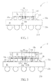
- FIG. 1 is a schematic, cross-sectional diagram showing a microelectronic package such as a flip-chip BGA (FCBGA) package in accordance with one embodiment of the invention.
- the microelectronic package 1 includes a packaging substrate 20 having a chip mounting surface 20a and a bottom surface 20b.
- a chip 10 is mounted on the chip mounting surface 20a of the packaging substrate 20.
- a plurality of solder balls 210 are implanted on the bottom surface 20b.
- the chip 10 has an active surface 10a.
- a plurality of input/output (I/O) pads 11 are provided on the active surface 10a.
- the chip 10 is flipped and is assembled face-down to the chip mounting surface 20a.
- the chip 10 is electrically connected to the packaging substrate 20 through a plurality of bumps 110 to form a flip-chip BGA package.
- the bumps 110 have a bump height h.
- An underfill 120 may be optionally provided between the bumps 110 underneath the chip 10.
- a discrete passive element 30 such as a decoupling capacitor, a resistor, an inductor, or any suitable integrated passive device (IPD) is mounted directly on the active surface 10a of the chip 10.
- the discrete passive element 30 is a decoupling capacitor and includes a terminal 302 and a terminal 304.
- the terminals 302 and 304 may be electrically connected to a ground I/O pad 11a and a power I/O pad 11b respectively.
- the discrete passive element 30 may be directly mounted on the active surface 10a by using a surface mounting technology (SMT) or any suitable soldering process.
- the discrete passive element 30 has thickness t that is smaller than the bump height h.
- the thickness t is less than 80 micrometers, but not limited thereto.
- FIG. 2 is a schematic, cross-sectional diagram showing a microelectronic package such as a Fan-Out Wafer-Level-Package (Fan-Out WLP) in accordance with another embodiment of the invention, wherein like numeral numbers designate like regions, layers or elements.
- the microelectronic package 2 includes a packaging substrate 20 having a chip mounting surface 20a and a bottom surface 20b.
- a chip 10 is mounted on the chip mounting surface 20a of the packaging substrate 20.
- a plurality of solder balls 210 are implanted on the bottom surface 20b.
- the chip 10 has an active surface 10a and four side edges 10b.
- the four side edges 10b of the chip 10 are encapsulated and surrounded by a molding compound 12.
- a plurality of input/output (I/O) pads 11 are provided on the active surface 10a and on the molding compound 12.
- a rewiring or redistribution layer (RDL) structure 13 is formed directly on the active surface 10a to fan out the I/O pads 11 to thereby form a plurality of bump pads 131 having a looser pad pitch.
- the bumps 110 have a bump height h.
- An underfill 120 may be optionally provided between the bumps 110 underneath the chip 10. The details of the wiring and dielectric layers of the RDL structure 13 are not explicitly shown.
- a discrete passive element 30 such as a decoupling capacitor, a resistor, or an inductor is mounted directly on the RDL structure 13.
- the discrete passive element 30 is a decoupling capacitor and includes a terminal 302 and a terminal 304.
- the terminals 302 and 304 may be electrically connected to a bump pad 131a that is related to a ground I/O pad on the active surface 11a and a bump pad 131b that is related to a power I/O pad 11b respectively.
- the discrete passive element 30 may be directly mounted on the RDL structure 13 by using a surface mounting technology (SMT).
- SMT surface mounting technology
- the discrete passive element 30 has thickness t that is smaller than the bump height h.
- the thickness t is less than 80 micrometers, but not limited thereto.
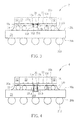
- FIG. 3 is a schematic, cross-sectional diagram showing a microelectronic package such as a Fan-Out WLP in accordance with another embodiment of the invention, wherein like numeral numbers designate like regions, layers or elements.
- the microelectronic package 3 includes a packaging substrate 20 having a chip mounting surface 20a and a bottom surface 20b.
- a chip 10 is mounted on the chip mounting surface 20a of the packaging substrate 20.
- a plurality of solder balls 210 are implanted on the bottom surface 20b.
- the chip 10 has an active surface 10a and four side edges 10b.
- the four side edges 10b of the chip 10 are encapsulated and surrounded by a molding compound 12.
- a plurality of input/output (I/O) pads 11 are provided on the active surface 10a.
- An RDL structure 13 is formed directly on the active surface 10a to fan out the I/O pads 11 to thereby form a plurality of bump pads 131 having a looser pad pitch.
- the bumps 110 have a bump height h.
- the bump height h may be smaller than 80 micrometers.
- An underfill 120 may be optionally provided between the bumps 110.
- the details of the wiring and dielectric layers of the RDL structure 13 are not explicitly shown.
- a discrete passive element 30 such as a decoupling capacitor, a resistor, or an inductor is mounted within a cavity 133 recessed into the RDL structure 13.
- the discrete passive element 30 is a decoupling capacitor and includes a terminal 302 and a terminal 304.
- the terminals 302 and 304 may be electrically connected to a bump pad 131a that is related to a ground I/O pad on the active surface 11a and a bump pad 131b that is related to a power I/O pad 11b respectively.
- the bump pads 131a and 131b are disposed at the bottom surface of the cavity 133.
- the discrete passive element 30 may be directly mounted within the cavity 133 by using a surface mounting technology (SMT).
- SMT surface mounting technology
- the discrete passive element 30 has thickness t that may be equal to or smaller than the bump height h.
- the thickness t is less than 80 micrometers, but not limited thereto.
- FIG. 4 is a schematic, cross-sectional diagram showing a microelectronic package such as a Fan-Out WLP in accordance with still another embodiment of the invention, wherein like numeral numbers designate like regions, layers or elements.
- the microelectronic package 4 includes a packaging substrate 20 having a chip mounting surface 20a and a bottom surface 20b.
- a chip 10 is mounted on the chip mounting surface 20a of the packaging substrate 20.
- a plurality of solder balls 210 are implanted on the bottom surface 20b.
- the chip 10 has an active surface 10a and four side edges 10b.
- the four side edges 10b of the chip 10 are encapsulated and surrounded by a molding compound 12.
- a plurality of input/output (I/O) pads 11 are provided on the active surface 10a.
- a rewiring or redistribution layer (RDL) structure 13 is formed directly on the active surface 10a to fan out the I/O pads 11 to thereby form a plurality of bump pads 131 having a looser pad pitch.
- the bumps 110 have a bump height h.
- An underfill 120 may be optionally provided between the bumps 110. The details of the wiring and dielectric layers of the RDL structure 13 are not explicitly shown.
- a discrete passive element 30 such as a decoupling capacitor, a resistor, or an inductor is mounted directly on the RDL structure 13.
- the discrete passive element 30 is a decoupling capacitor and includes a terminal 302 and a terminal 304.
- the terminals 302 and 304 may be electrically connected to a bump pad 131a that is related to a ground I/O pad on the active surface 11a and a bump pad 131b that is related to a power I/O pad 11b respectively.
- the discrete passive element 30 may be directly mounted on the RDL structure 13 by using a surface mounting technology (SMT).
- SMT surface mounting technology
- the discrete passive element 30 has thickness t that is larger than the bump height h.
- the thickness t is greater than 80 micrometers, but not limited thereto.
- a cavity 233 corresponding to the discrete passive element 30 is provided in the chip mounting surface 20a.
- the cavity 233 has a depth that is deep enough to accommodate the lower portion of the discrete passive element 30.
- the discrete passive element 30 is not in direct contact with the packaging substrate 20 and the underfill 120 may flow into the gap between the discrete passive element 30 and the packaging substrate 20.
Landscapes
- Engineering & Computer Science (AREA)
- Semiconductor Integrated Circuits (AREA)
- Power Engineering (AREA)
- Manufacturing & Machinery (AREA)
- Structures For Mounting Electric Components On Printed Circuit Boards (AREA)
Abstract
Description
- As system complexity and operational speeds increase, the power consumption of integrated circuits increases dramatically. Additionally, the IC supply voltage continues to drop with the inevitable scaling of VLSI technology.
- Reducing the nominal supply voltage is accompanied by a reduction in device noise margins, making components more vulnerable to power supply noise. This noise consists of the dynamic AC voltage fluctuation due to the frequency dependent distributed parasitics inherent in today's power distribution systems, and the DC voltage drop (i.e., "IR" drop).
- In a microelectronic system, the system's IR drop may be budgeted into three portions: on-chip, package and board. On-chip IR drop has been extensively studied because the resistive loss is severe due to the fine feature-size of the on-die power grid.
- To reduce the IR drop and improve power integrity, decoupling capacitors are typically mounted on a top surface of a packaging substrate or disposed within the packaging substrate. However, the aforesaid substrate-level decoupling capacitors are still not close enough to the IC die in the package to cope with the on-chip IR drop.
- It is desirable to place a high-performance capacitor as close to the IC die as possible to shorten the transient response time.
- This in mind, the present invention aims at providing an improved microelectronic package with surface mounted passive element such as a decoupling capacitor disposed in close proximity to the IC die, which is capable of reducing the IR drop and improving power integrity, and is cost-effective.
- This is achieved by a microelectronic package according to the pre-characterizing clause of
claim 1. The dependent claims pertain to corresponding further developments and improvements. - As will be seen more clearly from the detailed description following below, the claimed microelectronic package includes a packaging substrate having a chip mounting surface; a chip mounted on the chip mounting surface of the packaging substrate with the chip's active surface facing down to the chip mounting surface; a plurality of input/output (I/O) pads distributed on the active surface of the chip; and a discrete passive element mounted on the active surface of the chip. The discrete passive element may be a decoupling capacitor, a resistor, or an inductor.
- According to another aspect of the invention, a microelectronic package includes a packaging substrate having a chip mounting surface; a chip mounted on the chip mounting surface of the packaging substrate with the chip's active surface facing down to the chip mounting surface; a plurality of input/output (I/O) pads distributed on the active surface of the chip; a redistribution layer (RDL) structure directly on the active surface of the chip between the chip and the chip mounting surface of the packaging substrate; and a discrete passive element mounted on the RDL structure. A plurality of bumps is disposed on RDL structure.
- These and other objectives of the present invention will no doubt become obvious to those of ordinary skill in the art after reading the following detailed description of the preferred embodiment that is illustrated in the various figures and drawings.
- In the following, the invention is further illustrated by way of example, taking reference to the accompanying drawings. Thereof
-
FIG. 1 is a schematic, cross-sectional diagram showing a microelectronic package such as a flip-chip BGA (FCBGA) package in accordance with one embodiment of the invention; -
FIG. 2 is a schematic, cross-sectional diagram showing a microelectronic package such as a Fan-Out Wafer-Level-Package (Fan-Out WLP) in accordance with another embodiment of the invention; -
FIG. 3 is a schematic, cross-sectional diagram showing a microelectronic package such as a Fan-Out WLP in accordance with another embodiment of the invention; and -
FIG. 4 is a schematic, cross-sectional diagram showing a microelectronic package such as a Fan-Out WLP in accordance with still another embodiment of the invention. - In the following detailed description of embodiments of the invention, reference is made to the accompanying drawings, which form a part hereof, and in which is shown by way of illustration specific preferred embodiments in which the disclosure may be practiced.
- These embodiments are described in sufficient detail to enable those skilled in the art to practice them, and it is to be understood that other embodiments may be utilized and that mechanical, chemical, electrical, and procedural changes may be made without departing from the spirit and scope of the present disclosure. The following detailed description is, therefore, not to be taken in a limiting sense, and the scope of embodiments of the present invention is defined only by the appended claims.
- The present invention pertains to an improved microelectronic package with at least one embedded, discrete decoupling capacitor that is disposed in close proximity to the IC die in the chip package. The embedded, thin decoupling capacitor effectively reduces on-chip IR drop.
-
FIG. 1 is a schematic, cross-sectional diagram showing a microelectronic package such as a flip-chip BGA (FCBGA) package in accordance with one embodiment of the invention. As shown inFIG. 1 , themicroelectronic package 1 includes apackaging substrate 20 having achip mounting surface 20a and abottom surface 20b. Achip 10 is mounted on thechip mounting surface 20a of thepackaging substrate 20. A plurality ofsolder balls 210 are implanted on thebottom surface 20b. - The
chip 10 has anactive surface 10a. A plurality of input/output (I/O)pads 11 are provided on theactive surface 10a. Thechip 10 is flipped and is assembled face-down to thechip mounting surface 20a. Thechip 10 is electrically connected to thepackaging substrate 20 through a plurality ofbumps 110 to form a flip-chip BGA package. Thebumps 110 have a bump height h. Anunderfill 120 may be optionally provided between thebumps 110 underneath thechip 10. - According to the illustrative embodiment, a discrete
passive element 30 such as a decoupling capacitor, a resistor, an inductor, or any suitable integrated passive device (IPD) is mounted directly on theactive surface 10a of thechip 10. According to the illustrative embodiment, the discretepassive element 30 is a decoupling capacitor and includes aterminal 302 and aterminal 304. According to the illustrative embodiment, theterminals O pad 11a and a power I/O pad 11b respectively. - According to the illustrative embodiment, the discrete
passive element 30 may be directly mounted on theactive surface 10a by using a surface mounting technology (SMT) or any suitable soldering process. According to the illustrative embodiment, the discretepassive element 30 has thickness t that is smaller than the bump height h. For example, the thickness t is less than 80 micrometers, but not limited thereto. -
FIG. 2 is a schematic, cross-sectional diagram showing a microelectronic package such as a Fan-Out Wafer-Level-Package (Fan-Out WLP) in accordance with another embodiment of the invention, wherein like numeral numbers designate like regions, layers or elements. As shown inFIG. 2 , likewise, themicroelectronic package 2 includes apackaging substrate 20 having achip mounting surface 20a and abottom surface 20b. Achip 10 is mounted on thechip mounting surface 20a of thepackaging substrate 20. A plurality ofsolder balls 210 are implanted on thebottom surface 20b. - The
chip 10 has anactive surface 10a and fourside edges 10b. The fourside edges 10b of thechip 10 are encapsulated and surrounded by amolding compound 12. A plurality of input/output (I/O)pads 11 are provided on theactive surface 10a and on themolding compound 12. A rewiring or redistribution layer (RDL)structure 13 is formed directly on theactive surface 10a to fan out the I/O pads 11 to thereby form a plurality ofbump pads 131 having a looser pad pitch. Thebumps 110 have a bump height h. Anunderfill 120 may be optionally provided between thebumps 110 underneath thechip 10. The details of the wiring and dielectric layers of theRDL structure 13 are not explicitly shown. - According to the illustrative embodiment, a discrete
passive element 30 such as a decoupling capacitor, a resistor, or an inductor is mounted directly on theRDL structure 13. According to the illustrative embodiment, the discretepassive element 30 is a decoupling capacitor and includes aterminal 302 and aterminal 304. According to the illustrative embodiment, theterminals bump pad 131a that is related to a ground I/O pad on theactive surface 11a and abump pad 131b that is related to a power I/O pad 11b respectively. - According to the illustrative embodiment, the discrete
passive element 30 may be directly mounted on theRDL structure 13 by using a surface mounting technology (SMT). According to the illustrative embodiment, the discretepassive element 30 has thickness t that is smaller than the bump height h. For example, the thickness t is less than 80 micrometers, but not limited thereto. -
FIG. 3 is a schematic, cross-sectional diagram showing a microelectronic package such as a Fan-Out WLP in accordance with another embodiment of the invention, wherein like numeral numbers designate like regions, layers or elements. As shown inFIG. 3 , likewise, themicroelectronic package 3 includes apackaging substrate 20 having achip mounting surface 20a and abottom surface 20b. Achip 10 is mounted on thechip mounting surface 20a of thepackaging substrate 20. A plurality ofsolder balls 210 are implanted on thebottom surface 20b. - The
chip 10 has anactive surface 10a and fourside edges 10b. The fourside edges 10b of thechip 10 are encapsulated and surrounded by amolding compound 12. A plurality of input/output (I/O)pads 11 are provided on theactive surface 10a. AnRDL structure 13 is formed directly on theactive surface 10a to fan out the I/O pads 11 to thereby form a plurality ofbump pads 131 having a looser pad pitch. Thebumps 110 have a bump height h. For example, the bump height h may be smaller than 80 micrometers. Anunderfill 120 may be optionally provided between thebumps 110. The details of the wiring and dielectric layers of theRDL structure 13 are not explicitly shown. - According to the illustrative embodiment, a discrete
passive element 30 such as a decoupling capacitor, a resistor, or an inductor is mounted within acavity 133 recessed into theRDL structure 13. According to the illustrative embodiment, the discretepassive element 30 is a decoupling capacitor and includes a terminal 302 and a terminal 304. According to the illustrative embodiment, theterminals bump pad 131a that is related to a ground I/O pad on theactive surface 11a and abump pad 131b that is related to a power I/O pad 11b respectively. Thebump pads cavity 133. - According to the illustrative embodiment, the discrete
passive element 30 may be directly mounted within thecavity 133 by using a surface mounting technology (SMT). According to the illustrative embodiment, the discretepassive element 30 has thickness t that may be equal to or smaller than the bump height h. For example, the thickness t is less than 80 micrometers, but not limited thereto. -
FIG. 4 is a schematic, cross-sectional diagram showing a microelectronic package such as a Fan-Out WLP in accordance with still another embodiment of the invention, wherein like numeral numbers designate like regions, layers or elements. As shown inFIG. 4 , likewise, themicroelectronic package 4 includes apackaging substrate 20 having achip mounting surface 20a and abottom surface 20b. Achip 10 is mounted on thechip mounting surface 20a of thepackaging substrate 20. A plurality ofsolder balls 210 are implanted on thebottom surface 20b. - The
chip 10 has anactive surface 10a and fourside edges 10b. The fourside edges 10b of thechip 10 are encapsulated and surrounded by amolding compound 12. A plurality of input/output (I/O)pads 11 are provided on theactive surface 10a. A rewiring or redistribution layer (RDL)structure 13 is formed directly on theactive surface 10a to fan out the I/O pads 11 to thereby form a plurality ofbump pads 131 having a looser pad pitch. Thebumps 110 have a bump height h. Anunderfill 120 may be optionally provided between thebumps 110. The details of the wiring and dielectric layers of theRDL structure 13 are not explicitly shown. - According to the illustrative embodiment, a discrete
passive element 30 such as a decoupling capacitor, a resistor, or an inductor is mounted directly on theRDL structure 13. According to the illustrative embodiment, the discretepassive element 30 is a decoupling capacitor and includes a terminal 302 and a terminal 304. According to the illustrative embodiment, theterminals bump pad 131a that is related to a ground I/O pad on theactive surface 11a and abump pad 131b that is related to a power I/O pad 11b respectively. - According to the illustrative embodiment, the discrete
passive element 30 may be directly mounted on theRDL structure 13 by using a surface mounting technology (SMT). According to the illustrative embodiment, the discretepassive element 30 has thickness t that is larger than the bump height h. For example, the thickness t is greater than 80 micrometers, but not limited thereto. - Since the discrete
passive element 30 has thickness t that is larger than the bump height h, acavity 233 corresponding to the discretepassive element 30 is provided in thechip mounting surface 20a. Thecavity 233 has a depth that is deep enough to accommodate the lower portion of the discretepassive element 30. According to the illustrative embodiment, the discretepassive element 30 is not in direct contact with thepackaging substrate 20 and theunderfill 120 may flow into the gap between the discretepassive element 30 and thepackaging substrate 20.
Claims (14)
- A microelectronic package (1, 2, 3, 4), characterized by:a packaging substrate (20) having a chip mounting surface (20a);a chip (10) mounted on the chip mounting surface (20a) of the packaging substrate (20) with the chip's active surface (10a) facing down to the chip mounting surface (20a);a plurality of input/output (I/O) pads (11, 11a, 11b) distributed on the active surface (10a) of the chip (10); anda discrete passive element (30) disposed between the active surface (10a) and the chip mounting surface (20a).
- The microelectronic package according to claim 1, further characterized in that the discrete passive element (30) comprises a decoupling capacitor, a resistor, or an inductor.
- The microelectronic package according to claim 1, further characterized in that the I/O pads (11) comprise a ground I/O pad (11a) and a power I/O pad (11b).
- The microelectronic package according to claim 3, further characterized in that the discrete passive element (30) is a decoupling capacitor comprising a first terminal (302) and a second terminal (304), and wherein the first terminal (302) and the second terminal (304) are electrically connected to the ground I/O pad (11a) and the power I/O pad (11b), respectively.
- The microelectronic package according to claim 1, further characterized in that the discrete passive element (30) is directly mounted on the active surface (10a) of the chip (10).
- The microelectronic package according to claim 1, further characterized in that a redistribution layer (RDL) structure (13) is directly disposed on the active surface (10a) of the chip (10) and between the chip (10) and the chip mounting surface (20a) of the packaging substrate (20).
- The microelectronic package according to claim 6, further characterized in that the discrete passive element (30) is directly mounted on the RDL structure (13).
- The microelectronic package according to claim 7, further characterized in that the discrete passive element (30) is disposed within a cavity (133) recessed into the RDL structure (13).
- The microelectronic package according to claim 6, further characterized in that four side edges of the chip (10) are encapsulated and surrounded by a molding compound (12).
- The microelectronic package according to claim 1, further characterized in that a plurality of bumps (110) is disposed between the active surface (10a) and the chip mounting surface (20a), and wherein the plurality of bumps (110) has a bump height.
- The microelectronic package according to claim 10, further characterized in that the discrete passive element (30) has a thickness smaller than the bump height.
- The microelectronic package according to claim 10, further characterized in that the discrete passive element (30) has a thickness greater than the bump height.
- The microelectronic package according to claim 12, further characterized in that a cavity (233) corresponding to the discrete passive element (30) is disposed in the chip mounting surface (20a) of the packaging substrate (20), and wherein the cavity (233) has a depth that is deep enough to accommodate a lower portion of the discrete passive element (30).
- The microelectronic package according to claim 1, further characterized in that an underfill (120) is disposed between the bumps (110) underneath the chip (10).
Applications Claiming Priority (3)
| Application Number | Priority Date | Filing Date | Title |
|---|---|---|---|
| US201562105435P | 2015-01-20 | 2015-01-20 | |
| US201562134014P | 2015-03-17 | 2015-03-17 | |
| US14/925,995 US9660017B2 (en) | 2015-01-20 | 2015-10-29 | Microelectronic package with surface mounted passive element |
Publications (2)
| Publication Number | Publication Date |
|---|---|
| EP3057132A2 true EP3057132A2 (en) | 2016-08-17 |
| EP3057132A3 EP3057132A3 (en) | 2016-11-09 |
Family
ID=54770915
Family Applications (1)
| Application Number | Title | Priority Date | Filing Date |
|---|---|---|---|
| EP15197168.6A Ceased EP3057132A3 (en) | 2015-01-20 | 2015-12-01 | Microelectronic package with surface mounted passive element |
Country Status (3)
| Country | Link |
|---|---|
| US (1) | US9660017B2 (en) |
| EP (1) | EP3057132A3 (en) |
| CN (1) | CN105810676A (en) |
Families Citing this family (11)
| Publication number | Priority date | Publication date | Assignee | Title |
|---|---|---|---|---|
| DE102014118769B4 (en) | 2014-12-16 | 2017-11-23 | Infineon Technologies Ag | Pressure sensor module with a sensor chip and passive components within a common housing |
| US20200068711A1 (en) * | 2016-11-23 | 2020-02-27 | Intel IP Corporation | Component terminations for semiconductor packages |
| US20180294255A1 (en) * | 2017-04-11 | 2018-10-11 | Mediatek Inc. | Method for fabricating microelectronic package with surface mounted passive element |
| US11264315B2 (en) * | 2017-09-29 | 2022-03-01 | Intel Corporation | Electronic package with passive component between substrates |
| US10892316B2 (en) * | 2018-11-15 | 2021-01-12 | Google Llc | High density ball grid array (BGA) package capacitor design |
| CN110676185A (en) * | 2019-09-12 | 2020-01-10 | 无锡江南计算技术研究所 | Novel fine-pitch BGA packaging structure and filter capacitor design method |
| CN113270388A (en) * | 2020-02-14 | 2021-08-17 | 达发科技(苏州)有限公司 | Integrated circuit packaging structure |
| US11887976B2 (en) * | 2020-10-26 | 2024-01-30 | Mediatek Inc. | Land-side silicon capacitor design and semiconductor package using the same |
| US20220130741A1 (en) * | 2020-10-27 | 2022-04-28 | Qualcomm Incorporated | Package structure for passive component to die critical distance reduction |
| US20230317693A1 (en) * | 2022-03-29 | 2023-10-05 | nD-HI Technologies Lab, Inc. | Die package, ic package and manufacturing process thereof |
| US20250149524A1 (en) * | 2023-11-03 | 2025-05-08 | Taiwan Semiconductor Manufacturing Company Limited | Package structure including a redistribution layer (rdl) structure with a recessed portion and methods of forming the same |
Citations (2)
| Publication number | Priority date | Publication date | Assignee | Title |
|---|---|---|---|---|
| US20020074669A1 (en) * | 2000-12-15 | 2002-06-20 | Mitsubishi Denki Kabushiki Kaisha | Semiconductor device having capacitors for reducing power source noise |
| JP2004069692A (en) * | 2002-07-23 | 2004-03-04 | Fujitsu Ltd | Thin film capacitors |
Family Cites Families (14)
| Publication number | Priority date | Publication date | Assignee | Title |
|---|---|---|---|---|
| JP2942363B2 (en) | 1991-01-14 | 1999-08-30 | 株式会社日立製作所 | Semiconductor integrated circuit device |
| US6563192B1 (en) * | 1995-12-22 | 2003-05-13 | Micron Technology, Inc. | Semiconductor die with integral decoupling capacitor |
| US6801422B2 (en) * | 1999-12-28 | 2004-10-05 | Intel Corporation | High performance capacitor |
| US6584328B1 (en) * | 2000-01-10 | 2003-06-24 | Compal Electronics, Inc. | Wireless communication system that uses keywords to find and display map graphic data |
| US7067914B2 (en) * | 2001-11-09 | 2006-06-27 | International Business Machines Corporation | Dual chip stack method for electro-static discharge protection of integrated circuits |
| JP4077261B2 (en) * | 2002-07-18 | 2008-04-16 | 富士通株式会社 | Semiconductor device |
| US20040022038A1 (en) * | 2002-07-31 | 2004-02-05 | Intel Corporation | Electronic package with back side, cavity mounted capacitors and method of fabrication therefor |
| TW578292B (en) * | 2002-11-22 | 2004-03-01 | Via Tech Inc | Chip to eliminate noise and manufacturing method thereof |
| US8368150B2 (en) * | 2003-03-17 | 2013-02-05 | Megica Corporation | High performance IC chip having discrete decoupling capacitors attached to its IC surface |
| US7791192B1 (en) * | 2006-01-27 | 2010-09-07 | Xilinx, Inc. | Circuit for and method of implementing a capacitor in an integrated circuit |
| JP4734282B2 (en) * | 2007-04-23 | 2011-07-27 | 株式会社日立製作所 | Semiconductor chip and semiconductor device |
| SG148054A1 (en) * | 2007-05-17 | 2008-12-31 | Micron Technology Inc | Semiconductor packages and method for fabricating semiconductor packages with discrete components |
| US8367470B2 (en) * | 2009-08-07 | 2013-02-05 | Stats Chippac, Ltd. | Semiconductor device and method of forming cavity in build-up interconnect structure for short signal path between die |
| US20140374877A1 (en) * | 2013-06-21 | 2014-12-25 | Altera Corporation | Integrated Circuits With On-Die Decoupling Capacitors |
-
2015
- 2015-10-29 US US14/925,995 patent/US9660017B2/en active Active
- 2015-11-11 CN CN201510769418.3A patent/CN105810676A/en active Pending
- 2015-12-01 EP EP15197168.6A patent/EP3057132A3/en not_active Ceased
Patent Citations (2)
| Publication number | Priority date | Publication date | Assignee | Title |
|---|---|---|---|---|
| US20020074669A1 (en) * | 2000-12-15 | 2002-06-20 | Mitsubishi Denki Kabushiki Kaisha | Semiconductor device having capacitors for reducing power source noise |
| JP2004069692A (en) * | 2002-07-23 | 2004-03-04 | Fujitsu Ltd | Thin film capacitors |
Also Published As
| Publication number | Publication date |
|---|---|
| EP3057132A3 (en) | 2016-11-09 |
| US20160211318A1 (en) | 2016-07-21 |
| US9660017B2 (en) | 2017-05-23 |
| CN105810676A (en) | 2016-07-27 |
Similar Documents
| Publication | Publication Date | Title |
|---|---|---|
| US9660017B2 (en) | Microelectronic package with surface mounted passive element | |
| US11810867B2 (en) | Wire bond wires for interference shielding | |
| EP3051585A1 (en) | Chip package with embedded passive device | |
| US11671010B2 (en) | Power delivery for multi-chip-package using in-package voltage regulator | |
| US9165877B2 (en) | Fan-out semiconductor package with copper pillar bumps | |
| US10199320B2 (en) | Method of fabricating electronic package | |
| US8183678B2 (en) | Semiconductor device having an interposer | |
| TWI624916B (en) | Semiconductor chip package member with better heat dissipation performance | |
| US20230261572A1 (en) | Power delivery for multi-chip-package using in-package voltage regulator | |
| US20130026609A1 (en) | Package assembly including a semiconductor substrate with stress relief structure | |
| EP3067928B1 (en) | Semiconductor package assembly with passive device | |
| CN118629966A (en) | Package structure | |
| US20230378072A1 (en) | Electronic package and manufacturing method thereof | |
| US11967559B2 (en) | Electronic package | |
| CN107275312A (en) | Passive element packaging part and the semiconductor module for including the passive element packaging part | |
| US20230066752A1 (en) | Semiconductor die package with ring structure and method for forming the same | |
| US20240249989A1 (en) | Selectively Dispensed Underfill and Edge Bond Patterns | |
| US20250054824A1 (en) | Package structure having dam structure | |
| US20230326889A1 (en) | Electronic package | |
| US12213247B2 (en) | Electronic device | |
| US9601423B1 (en) | Under die surface mounted electrical elements | |
| US12368104B2 (en) | Electronic package | |
| TW202518689A (en) | Electronic package | |
| KR20240146904A (en) | Semiconductor package with decoupling capacitor and method for manufacturing the same |
Legal Events
| Date | Code | Title | Description |
|---|---|---|---|
| PUAI | Public reference made under article 153(3) epc to a published international application that has entered the european phase |
Free format text: ORIGINAL CODE: 0009012 |
|
| AK | Designated contracting states |
Kind code of ref document: A2 Designated state(s): AL AT BE BG CH CY CZ DE DK EE ES FI FR GB GR HR HU IE IS IT LI LT LU LV MC MK MT NL NO PL PT RO RS SE SI SK SM TR |
|
| AX | Request for extension of the european patent |
Extension state: BA ME |
|
| PUAL | Search report despatched |
Free format text: ORIGINAL CODE: 0009013 |
|
| AK | Designated contracting states |
Kind code of ref document: A3 Designated state(s): AL AT BE BG CH CY CZ DE DK EE ES FI FR GB GR HR HU IE IS IT LI LT LU LV MC MK MT NL NO PL PT RO RS SE SI SK SM TR |
|
| AX | Request for extension of the european patent |
Extension state: BA ME |
|
| RIC1 | Information provided on ipc code assigned before grant |
Ipc: H01L 25/16 20060101AFI20161005BHEP Ipc: H01L 21/60 20060101ALN20161005BHEP |
|
| 17P | Request for examination filed |
Effective date: 20170509 |
|
| RBV | Designated contracting states (corrected) |
Designated state(s): AL AT BE BG CH CY CZ DE DK EE ES FI FR GB GR HR HU IE IS IT LI LT LU LV MC MK MT NL NO PL PT RO RS SE SI SK SM TR |
|
| 17Q | First examination report despatched |
Effective date: 20180903 |
|
| STAA | Information on the status of an ep patent application or granted ep patent |
Free format text: STATUS: THE APPLICATION HAS BEEN REFUSED |
|
| 18R | Application refused |
Effective date: 20190404 |