EP3056936A1 - Apparatus including optical deflector controlled by saw-tooth voltage and its controlling method - Google Patents
Apparatus including optical deflector controlled by saw-tooth voltage and its controlling method Download PDFInfo
- Publication number
- EP3056936A1 EP3056936A1 EP16155111.4A EP16155111A EP3056936A1 EP 3056936 A1 EP3056936 A1 EP 3056936A1 EP 16155111 A EP16155111 A EP 16155111A EP 3056936 A1 EP3056936 A1 EP 3056936A1
- Authority
- EP
- European Patent Office
- Prior art keywords
- voltage
- block
- offset characteristic
- integral
- straight line
- Prior art date
- Legal status (The legal status is an assumption and is not a legal conclusion. Google has not performed a legal analysis and makes no representation as to the accuracy of the status listed.)
- Withdrawn
Links
Images






Classifications
-
- G—PHYSICS
- G02—OPTICS
- G02B—OPTICAL ELEMENTS, SYSTEMS OR APPARATUS
- G02B26/00—Optical devices or arrangements for the control of light using movable or deformable optical elements
- G02B26/08—Optical devices or arrangements for the control of light using movable or deformable optical elements for controlling the direction of light
- G02B26/0816—Optical devices or arrangements for the control of light using movable or deformable optical elements for controlling the direction of light by means of one or more reflecting elements
- G02B26/0833—Optical devices or arrangements for the control of light using movable or deformable optical elements for controlling the direction of light by means of one or more reflecting elements the reflecting element being a micromechanical device, e.g. a MEMS mirror, DMD
- G02B26/0858—Optical devices or arrangements for the control of light using movable or deformable optical elements for controlling the direction of light by means of one or more reflecting elements the reflecting element being a micromechanical device, e.g. a MEMS mirror, DMD the reflecting means being moved or deformed by piezoelectric means
-
- G—PHYSICS
- G02—OPTICS
- G02B—OPTICAL ELEMENTS, SYSTEMS OR APPARATUS
- G02B26/00—Optical devices or arrangements for the control of light using movable or deformable optical elements
- G02B26/08—Optical devices or arrangements for the control of light using movable or deformable optical elements for controlling the direction of light
- G02B26/10—Scanning systems
- G02B26/105—Scanning systems with one or more pivoting mirrors or galvano-mirrors
-
- G—PHYSICS
- G09—EDUCATION; CRYPTOGRAPHY; DISPLAY; ADVERTISING; SEALS
- G09G—ARRANGEMENTS OR CIRCUITS FOR CONTROL OF INDICATING DEVICES USING STATIC MEANS TO PRESENT VARIABLE INFORMATION
- G09G3/00—Control arrangements or circuits, of interest only in connection with visual indicators other than cathode-ray tubes
- G09G3/02—Control arrangements or circuits, of interest only in connection with visual indicators other than cathode-ray tubes by tracing or scanning a light beam on a screen
- G09G3/025—Control arrangements or circuits, of interest only in connection with visual indicators other than cathode-ray tubes by tracing or scanning a light beam on a screen with scanning or deflecting the beams in two directions or dimensions
Definitions
- the presently disclosed subject matter relates to an apparatus including an optical deflector controlled by a saw-tooth voltage and its controlling method, and more specifically, to a video projection apparatus and its controlling method.
- the video projection apparatus can be used as a pico projector, a head mount display (HMD) unit, a head up display (HUD) unit and the like.
- a prior art video projection apparatus is constructed by a two-dimensional optical deflector as an optical scanner manufactured by a micro electro mechanical system (MEMS) device manufactured using a semiconductor process and micro machine technology (see: JP5543468B2 & US2010/0073748A1 ). Since the MEMS optical scanner is focus-free, the video projection apparatus can be small in size.
- MEMS micro electro mechanical system
- a mirror is rocked with respect to a horizontal deflection at a high frequency such as 18 kHz, while the mirror is rocked with respect to a vertical deflection at a low frequency such as 60 Hz (see: paragraph 0026 of US2010/0073748A1 ).
- the mirror includes a sensor for sensing rocking vibrations thereof in the vertical deflection.
- the vertical deflection of the mirror is controlled by the feedback of a simple sum of the sense voltage of the sensor, thus accurately realizing the vertical deflection of the mirror (see: the summing buffer 760 of Fig. 7 and 8 of US2010/0073748A1 ).
- the above-mentioned sensor can be constructed by a piezoelectric element incorporated into the optical deflector (see: US8730549B2 ).
- the fluctuation of a DC offset would be caused by the fluctuation of the piezoelectric coefficient of the piezoelectric sensor due to the fluctuation of environmental factors such as temperature and humidity and due to the fluctuation of hardness and rigidity of a substrate by the heating of the piezoelectric sensor irradiated by light. Also, the fluctuation of a DC offset would be caused by charges stored in the piezoelectric sensor when it is operated for a long time.
- the presently disclosed subject matter seeks to solve the above-described problem.
- the control unit includes: a saw-tooth voltage generating block adapted to generate a saw-tooth voltage; an integral block adapted to calculate an integral voltage of a sum of a sense voltage of the piezoelectric sensor and a DC offset characteristic voltage; a DC offset characteristic voltage calculating block adapted to calculate the DC offset characteristic voltage in accordance with the integral voltage; a subtracter block, connected to the saw tooth voltage generating block and the integral block and adapted to generate a deviation between the saw-tooth voltage and the integral voltage; and a controller, connected to the subtracter block and adapted to generate a drive voltage in accordance with the deviation to apply the drive voltage to the piezoelectric actuator.
- a method for controlling an optical deflector including: a mirror; a piezoelectric actuator adapted to rock the mirror around an axis of the mirror; and a piezoelectric sensor adapted to sense vibrations of the piezoelectric actuator
- the method includes: generating a saw-tooth voltage; calculating an integral voltage of a sum of a sense voltage of the piezoelectric sensor and a DC offset characteristic voltage; calculating the DC offset characteristic voltage in accordance with the integral voltage; generating a deviation between the saw-tooth voltage and the integral voltage; and generating a drive voltage in accordance with the deviation to apply the drive voltage to the piezoelectric actuator.
- the integral voltage includes the sense voltage and the DC offset characteristic voltage that represents a DC offset voltage generated in the piezoelectric sensor, the DC offset voltage can be compensated for by the integral voltage, so that the deflection of the mirror can accurately be controlled.
- a video projection apparatus 1 receives a video signal VS from a video source such as a personal computer or a camera system to generate a laser beam L for a screen 2.
- the video projection apparatus 1 is constructed by a video signal input unit 11, a video signal processing section 12, a frame memory 13 and a control section 14 for controlling the video signal processing section 12 and the frame memory 13.
- the video signal input unit 11 is an analog red/green/blue (RGB) receiver or a digital video signal receiver such as a digital video interface (DVI), or a high-definition multimedia interface (HDMI).
- Video signals received by the video signal input unit 11 are processed by a video signal processing section 12 and are stored in the frame memory 13 frame by frame. For example, 60 frames per second are stored in the frame memory 13.
- the frame memory 13 is formed by a high-speed random access memory (RAM) such as an SDRAM, a DDR2 SDRAM or a DDR3 SDRAM.
- one frame of the frame memory 13 corresponds to a view field formed by a horizontal angle of 40° and a vertical angle of 25° (see: Fig. 6 ).
- the video projection apparatus 1 is constructed by a drive voltage generating section 15, a drive voltage processing section 16, and a pixel data extracting section 17.
- the drive voltage generating section 15 generates digital drive voltages V xa and V ya which are transmitted via a drive unit 18 formed by digital-to-analog (D/A) converters 181 and 182, amplifiers 183 and 184, and inverters 185 and 186 to a MEMS optical deflector 19.
- analog drive voltages V xa and V ya and their inverted drive voltages V xb and V yb are supplied from the drive unit 18 to the MEMS optical deflector 19.
- the analog drive voltages V ya and V yb are represented by the same denotations of the digital drive voltages V ya and V yb , in order to simplify the description.
- the MEMS optical deflector 19 generates sense voltages U xsa , V xsb , V ysa and V ysb in response to the flexing angles of the mirror thereof which are supplied via a sense voltage input unit 20 formed by a subtracter 201, an adder 202, a band-pass filter 203, a low-pass filter 204, and analog-to-digital (A/D) converters 205 and 206 to the drive voltage processing section 16.
- a sense voltage input unit 20 formed by a subtracter 201, an adder 202, a band-pass filter 203, a low-pass filter 204, and analog-to-digital (A/D) converters 205 and 206 to the drive voltage processing section 16.
- the A/D converter 205 performs an A/D conversion upon the output voltage of the band-pass filter 203 to transmit a digital sense voltage V xs to the drive voltage processing section 16, while the A/D converter 206 performs an A/D conversion upon the output voltage of the low-pass filter 204 to transmit a digital sense voltage V ys to the drive voltage processing section 16.
- the digital sense voltages V ys and V ys are represented by the same denotations of the analog output voltages V ys and V ys of the subtracter 201 and the adder 202, in order to simplify the description.
- the pixel data extracting section 17 generates a drive voltage which is supplied to a light source drive unit 21 formed by a D/A converter 211 and an amplifier 212 for supplying a drive current I d to a laser light source 22.
- the light source drive unit 21 and the laser light source 22 can be provided for each of red (R), green (G) and blue (B).
- the laser light source 22 can be replaced by a light emitting diode (LED) source.
- the drive voltage generating section 15, the drive voltage processing section 16 and the pixel data extracting section 17 are controlled by the control section 14.
- the drive voltage generating section 15 transmits extracting timing signals of pixel data to the pixel data extracting section 17.
- the drive voltage processing section 16 receives drive voltages similar to the drive voltages V xa and V ya from the drive voltage generating section 15 and the sense voltages V xs and V ys from the sense voltage input unit 20 to transmit a delay timing signal to the pixel data extracting section 17 due to the delay transmission of the drive voltages V xa and V ya to the mirror of the MEMS optical deflector 19.
- the pixel data extracting section 17 extracts pixel data from the frame memory 13 in accordance with the extracting timing signals of the drive voltage generating section 15 and the delay signal of the drive voltage processing section 16.
- the video signal processing section 12, the control section 14, the drive voltage generating section 15, the drive voltage processing section 16 and the pixel data extracting section 17 can be formed by a single control unit 23 or a microcomputer using a field-programmable gate array (FPGA), an extensible processing platform (EPP) or a system-on-a-chip (SoC).
- the control section 14 has an interface function with a universal asynchronous receiver transmitter (UART) and the like.
- the inner frame 192 is rectangularly-framed to surround the mirror 191 associated with the inner piezoelectric actuators 193a and 193b.
- the torsion bars 194a and 194b are arranged along the X-axis, and have ends coupled to the inner circumference of the inner frame 192 and other ends coupled to the outer circumference of the mirror 191. Therefore, the torsion bars 194a and 194b are twisted by the inner piezoelectric actuators 193a and 193b to rock the mirror 191 with respect to the X-axis.
- the inner piezoelectric actuators 193a and 193b oppose each other along the Y-axis and sandwich the torsion bars 194a and 194b.
- the inner piezoelectric actuators 193a and 193b have ends coupled to the inner circumference of the inner frame 192 and other ends coupled to the torsion bars 194a and 194b. In this case, the flexing direction of the inner piezoelectric actuator 193a is opposite to that of the inner piezoelectric actuator 193b.
- the outer frame 195 is rectangularly-framed to surround the inner frame 192 via the outer piezoelectric actuators 196a and 196b.
- the outer piezoelectric actuators 196a and 196b are coupled between the inner circumference of the outer frame 195 and the outer circumference of the inner frame 192, in order to rock the inner frame 192 associated with the mirror 191 with respect to the outer frame 195, i.e., to rock the mirror 191 with respect to the Y-axis.
- the outer piezoelectric actuator 196a is constructed by piezoelectric cantilevers 196a-1, 196a-2, 196a-3 and 196a-4 which are serially-coupled from the outer frame 195 to the inner frame 192. Also, each of the piezoelectric cantilevers 196a-1, 196a-2, 196a-3 and 196a-4 are in parallel with the X-axis of the mirror 191.
- the piezoelectric cantilevers 196a-1, 196a-2, 196a-3 and 196a-4 are folded at every cantilever or meandering from the outer frame 195 to the inner frame 192, so that the amplitudes of the piezoelectric cantilevers 196a-1, 196a-2, 196a-3 and 196a-4 can be changed along directions perpendicular to the Y-axis of the mirror 191.
- the outer piezoelectric actuator 196b is constructed by piezoelectric cantilevers 196b-1, 196b-2, 196b-3 and 196b-4 which are serially-coupled from the outer frame 195 to the inner frame 192. Also, each of the piezoelectric cantilevers 196b-1, 196b-2, 196b-3 and 196b-4 are in parallel with the X-axis of the mirror 191.
- the piezoelectric cantilevers 196b-1, 196b-2, 196b-3 and 196b-4 are folded at every cantilever or meandering from the outer frame 195 to the inner frame 192, so that the amplitudes of the piezoelectric cantilevers 196b-1, 196b-2, 196b-3 and 196b-4 can be changed along directions perpendicular to the Y-axis of the mirror 191.
- the number of piezoelectric cantilevers in the outer piezoelectric actuator 196a and the number of piezoelectric cantilevers in the outer piezoelectric actuator 196b can be other values such as 2, 6, 8, ⁇ .
- the piezoelectric sensors 197a and 197b serve as speed sensors that sense deflecting angle deviations of the mirror 191 mainly caused by the inner piezoelectric actuators 193a and 193b.
- the sense voltages V xsa and V xsb of the piezoelectric sensors 197a and 197b are substantially the same as each other, and opposite in phase to each other. These two sense voltages V xsa and V xsb correspond to differentiated signals of the drive voltages V xa and V xb . Also, the difference voltage V xs (see: Fig. 1 ) between the two sense voltages V xsa and V xsb would cancel noises included therein.
- the piezoelectric sensors 198a and 198b serve as speed sensors that sense deflecting angle signals of the mirror 191 mainly caused by the outer piezoelectric actuators 196a and 196b.
- the mirror 191 is constructed by a monocrystalline silicon support layer serving as a vibration plate and a metal layer serving as a reflector.
- the inner frame 192, the torsion bars 194a and 194b and the outer frame 195 are constructed by the monocrystalline silicon support layer and the like.
- Each of the piezoelectric actuators 194a and 194b and the piezoelectric cantilevers 196a-1 to 196a-4 and 196b-1 to 196b-4 and the piezoelectric sensors 197a, 197b, 198a and 198b is constructed by a Pt lower electrode layer, a lead titanate zirconate (PZT) layer and a Pt upper electrode layer.
- PZT lead titanate zirconate
- the meander-type piezoelectric actuators 196a and 196b are described below.
- the piezoelectric cantilevers 196a-1, 196a-2, 196a-3, 196a-4, 196b-1 196b-2, 196b-3 and 196b-4 are divided into an odd-numbered group of the piezoelectric cantilevers 196a-1 and 196a-3; 196b-1 and 196b-3, and an even-numbered group of the piezoelectric cantilevers 196a-2 and 196a-4; 196b-2 and 196b-4 alternating with the odd-numbered group of the piezoelectric cantilevers 196a-1 and 196a-3; 196b-1 and 196b-3.
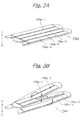
- Figs. 3A and 3B are perspective views for explaining the operation of the piezoelectric cantilevers of one outer piezoelectric actuator such as 196a of Fig. 2 .
- Fig. 3A illustrates a non-operation state of the piezoelectric cantilevers 196a-1, 196a-2, 196a-3 and 196a-4 of the piezoelectric actuator 196a
- Fig. 3B illustrates an operation state of the piezoelectric cantilevers 196a-1, 196a-2, 196a-3 and 196a-4 of the outer piezoelectric actuator 196a.
- Fig. 3B which illustrates only the piezoelectric cantilevers 196a-1, 196a-2, 196a-3 and 196a-4
- the odd-numbered group of the piezoelectric cantilevers 196a-1, 196a-3, 196b-1 and 196b-3 are flexed in one direction, for example, in a downward direction D
- the even-numbered group of the piezoelectric cantilevers 196a-2, 196a-4, 196b-2 and 196b-4 are flexed in the other direction, i.e., in an upward direction U.
- the mirror 191 is rocked with respect to the Y-axis.
- the drive voltage V xa and the drive voltage U xv generated from the drive unit 18 are sinusoidal at a relatively high resonant frequency f x and symmetrical or opposite in phase to each other.
- the inner piezoelectric actuators 193a and 193b carry out flexing operations in opposite directions to each other, so that the torsion bars 194a and 194b are twisted to rock the mirror 191 with respect to the X-axis.
- the changing rates of the drive voltages V xa and V xb are low at their lowest and highest levels as illustrated in Figs. 4A and 4B , so that the brightness thereof at the screen 2 would be particularly high. Therefore, as illustrated in Fig. 4C , horizontal blanking periods BP x for turning off the laser light source 22 are provided where the changing rates of the drive voltages V xa and V xb are low to make the brightness at the entire screen 2 uniform. Additionally, right-direction horizontal scanning periods RH alternating with left-direction horizontal scanning periods LH are provided between the horizontal blanking periods BP x , in order to increase the depicting time period, and thus the depicting efficiency can be enhanced.
- the drive voltage V ya and the drive voltage V yb are saw-tooth-shaped at a relatively low non-resonant frequency f Y and symmetrical or opposite in phase to each other.
- the piezoelectric cantilevers 196a-1, 196a-3, 196b-1 and 196b-3 and the piezoelectric cantilevers 196a-2, 196a-4, 196b-2 and 196b-4 carry out flexing operations in opposite directions to each other, so that the mirror 191 is rocked with respect to the Y-axis.
- the changing rate of the drive voltages V ya and V yb are low at their lowest and highest levels as illustrated in Figs. 5A and 5B , so that the brightness thereof at the screen 2 would be particularly high. Therefore, as illustrated in Fig. 5C , vertical blanking periods BP Y for turning off the laser light source 22 are provided where the changing rates of the drive voltages V ya and V yb are low to make the brightness at the entire screen 2 uniform.
- Fig. 6 which is a diagram illustrating a relationship between a scanning locus SL of the MEMS optical deflector 19 and a projected area of the laser beam L of the laser light source 22 of Fig. 1 , a horizontal scanning line H and a vertical scanning line V by the MEMS optical deflector 19 are protruded from a projected view field F of the laser beam L defined by a horizontal angle of 40° , for example, and a vertical angle of 25° , for example.
- the drive voltage generating section 15 includes a sinusoidal-wave voltage generating block (not shown) for generating a sinusoidal-wave voltage V ya and a phase-locked loop block (not shown) for transmitting the sinusoidal-wave voltage V ya to the drive unit 18.
- the drive voltage processing section 16 receives the sense voltage V xs from the sense voltage input unit 20, to calculate an integral voltage V xs ' of the sense voltage V xs , the integral voltage V xs ' is transmitted to the drive voltage generating section 15, so that the phase-locked loop block generates the sinusoidal-wave voltage V xa phase-locked to the integral voltage V xs '.
- Fig. 7 is a functional block circuit diagram of the drive voltage generating section 15 and the drive voltage processing section 16 of Fig. 1 .
- the drive voltage generating section 15 is constructed by a saw-tooth voltage generating block 151 operated by the control section 14, a subtracter block 152, and a proportional/integral/derivative (PID) controller 153 formed by a proportional block 1531, an integral block 1532, a derivative block 1583, and an adder block 1534.
- the drive voltage processing section 16 is constructed by a sum (or integral) block 161 and a DC offset characteristic voltage calculating block 162 for calculating a DC offset characteristic voltage C used in the integral block 161.
- the PID controller 153 can be another controller which includes only the proportional block 1531 and the integral block 1532, for example.
- the DC offset characteristic voltage C is calculated by the DC offset characteristic voltage calculating block 162 using a gradient of the integral voltage V ys ' with respect to time. Note that the DC offset characteristic voltage C is initialized at 0.
- the DC offset characteristic voltage calculating block 162 is constructed by a minimum point calculating block 1621 for calculating minimum points MIN 0 , MIN 1 , MIN 2 , ⁇ on the integral voltage V ys '.
- minimum points MIN 0 , MIN 1 , MIN 2 , ⁇ can be detected by differentiating the integral voltage V ys ' with respect to time, that is, rising points as minimum points can be detected in the differentiated integral voltage V ys '.
- minimum points MIN 0 , MIN 1 , MIN 2 , ⁇ are obtained (see: Figs. 11A, 11B and 11C ).
- the constant ⁇ is 2.
- the minimum point calculating block 1621 can be replaced by a maximum point calculating block which calculates maximum points MAX 0 , MAX 1 , MAX 2 , (see Figs. 11A, 11B and 11C ).
- the maximum points MAX 0 , MAX 1 , MAX 1 , ⁇ have a gradient tendency the same as that of the minimum points MIN 0 , MIN 1 , MIN 2 , ⁇ . Therefore, in this case, the straight line calculating block 1622 can calculate the same straight line using the maximum points MAX 0 , MAX 1 , MAX 2 , ⁇ .
- the operation of the adder 152 and the PID controller 153 of Fig.7 can be carried out by software illustrated by a flowchart in Fig. 8 executed at every time period T ms such as 1ms.
- a deviation "e” is calculated by e ⁇ V y ⁇ V ys ′
- a proportional term u p is calculated by u p ⁇ K p ⁇ e where K p is a proportional gain.
- an integral term u i is calculated by u i ⁇ u io + K i ⁇ T ⁇ e where u io is a previous integral term; and K i is an integral gain.
- a derivative term u d is calculated by u d ⁇ K d ⁇ e ⁇ e 0 / T
- a vertical drive voltage V ya is calculated by V ya ⁇ u p + u i + u d
- step 808 the vertical drive voltage V ya is transmitted to the drive unit 18.
- step 809 The flowchart of Fig. 8 is completed by step 809.
- the operation of the integral block 161 and the DC offset characteristic voltage calculating block 162 of Fig. 7 can be carried out by software illustrated by a flowchart in Fig. 9 executed at every time period T ms such as 1 ms. Note that a DC offset characteristic voltage C is initialized at 0. Also, counters "i" and "j" are initialized at 0.
- step 901 the counter "i" is counted up by +1.
- step 902 it is determined whether or not i ⁇ i m is satisfied.
- i m is 500 corresponding to 500 ms, for example.
- the control proceeds to steps 903 through 906 which calculate the DC offset characteristic voltage C, while if i ⁇ i m , the control proceeds directly to step 907.
- Steps 903 through 906 are explained later.
- the integral voltage V ys ' is renewed by V ys ′ ⁇ V ys ′ + V ys + C ⁇ T
- step 908 it is determined whether or not i ⁇ 3 is satisfied. As a result, if i ⁇ 3, the control proceeds to step 909. Otherwise, i.e., if i ⁇ 3, the control proceeds directly to step 912.
- Steps 903 to 906 are explained below.
- a DC offset characteristic voltage C is calculated by C ⁇ A / ⁇ where ⁇ ; is a constant larger than 1, preferably, 2.
- the second-previous integral voltage V ys2 ' is replaced by the previous integral voltage V ys1 '
- the previous integral voltage V ys1 ' is replaced by the current integral voltage V ys '.
- step 909 it can be determined whether or not the following formula is satisfied: V ys 2 ′ ⁇ V ys 1 ′ > V ys ′
Landscapes
- Physics & Mathematics (AREA)
- General Physics & Mathematics (AREA)
- Engineering & Computer Science (AREA)
- Optics & Photonics (AREA)
- Computer Hardware Design (AREA)
- Theoretical Computer Science (AREA)
- Mechanical Optical Scanning Systems (AREA)
- Mechanical Light Control Or Optical Switches (AREA)
- Micromachines (AREA)
- Transforming Electric Information Into Light Information (AREA)
- Control Of Indicators Other Than Cathode Ray Tubes (AREA)
Abstract
Description
- This application claims the priority benefit under 35 U.S.C. §119 to Japanese Patent Application No.
JP2015-025221 filed on February 12, 2015 - The presently disclosed subject matter relates to an apparatus including an optical deflector controlled by a saw-tooth voltage and its controlling method, and more specifically, to a video projection apparatus and its controlling method. The video projection apparatus can be used as a pico projector, a head mount display (HMD) unit, a head up display (HUD) unit and the like.
- A prior art video projection apparatus is constructed by a two-dimensional optical deflector as an optical scanner manufactured by a micro electro mechanical system (MEMS) device manufactured using a semiconductor process and micro machine technology (see:
JP5543468B2 US2010/0073748A1 ). Since the MEMS optical scanner is focus-free, the video projection apparatus can be small in size. - Generally, in the above-mentioned two-dimensional optical deflector, a mirror is rocked with respect to a horizontal deflection at a high frequency such as 18 kHz, while the mirror is rocked with respect to a vertical deflection at a low frequency such as 60 Hz (see: paragraph 0026 of
US2010/0073748A1 ). Also, the mirror includes a sensor for sensing rocking vibrations thereof in the vertical deflection. As a result, the vertical deflection of the mirror is controlled by the feedback of a simple sum of the sense voltage of the sensor, thus accurately realizing the vertical deflection of the mirror (see: the summing buffer 760 ofFig. 7 and8 ofUS2010/0073748A1 ). On the other hand, the above-mentioned sensor can be constructed by a piezoelectric element incorporated into the optical deflector (see:US8730549B2 ). - In the above-described prior art video projection apparatus, however, since the sensor is susceptible to the fluctuation of a DC offset generated in the sense voltage thereof, it is difficult to accurately control the vertical deflection of the mirror. Also, if a circuit is added to exclude the above-mentioned fluctuation of a DC offset, the manufacturing cost would be increased. As a result, if the apparatus is a video projection apparatus, it is difficult to accurately control a projected view field.
- Note that the fluctuation of a DC offset would be caused by the fluctuation of the piezoelectric coefficient of the piezoelectric sensor due to the fluctuation of environmental factors such as temperature and humidity and due to the fluctuation of hardness and rigidity of a substrate by the heating of the piezoelectric sensor irradiated by light. Also, the fluctuation of a DC offset would be caused by charges stored in the piezoelectric sensor when it is operated for a long time.
- The presently disclosed subject matter seeks to solve the above-described problem.
- According to the presently disclosed subject matter, in an apparatus including an optical deflector and a control unit for controlling the optical deflector, wherein the optical deflector includes a mirror; a piezoelectric actuator adapted to rock the mirror around an axis of the mirror; and a piezoelectric sensor adapted to sense vibrations of the piezoelectric actuator, the control unit includes: a saw-tooth voltage generating block adapted to generate a saw-tooth voltage; an integral block adapted to calculate an integral voltage of a sum of a sense voltage of the piezoelectric sensor and a DC offset characteristic voltage; a DC offset characteristic voltage calculating block adapted to calculate the DC offset characteristic voltage in accordance with the integral voltage; a subtracter block, connected to the saw tooth voltage generating block and the integral block and adapted to generate a deviation between the saw-tooth voltage and the integral voltage; and a controller, connected to the subtracter block and adapted to generate a drive voltage in accordance with the deviation to apply the drive voltage to the piezoelectric actuator.
- Also, in a method for controlling an optical deflector including: a mirror; a piezoelectric actuator adapted to rock the mirror around an axis of the mirror; and a piezoelectric sensor adapted to sense vibrations of the piezoelectric actuator, the method includes: generating a saw-tooth voltage; calculating an integral voltage of a sum of a sense voltage of the piezoelectric sensor and a DC offset characteristic voltage; calculating the DC offset characteristic voltage in accordance with the integral voltage; generating a deviation between the saw-tooth voltage and the integral voltage; and generating a drive voltage in accordance with the deviation to apply the drive voltage to the piezoelectric actuator.
- According to the presently disclosed subject matter, since the integral voltage includes the sense voltage and the DC offset characteristic voltage that represents a DC offset voltage generated in the piezoelectric sensor, the DC offset voltage can be compensated for by the integral voltage, so that the deflection of the mirror can accurately be controlled.
- The above and other advantages and features of the presently disclosed subject matter will be more apparent from the following description of certain embodiments, taken in conjunction with the accompanying drawings, wherein:
-
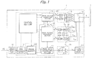
Fig. 1 is a block circuit diagram illustrating an embodiment of the apparatus according to the presently disclosed subject matter; -
Fig. 2 is a perspective view of the MEMS optical deflector ofFig. 1 ; -
Figs. 3A and 3B are perspective views for explaining the operation of the outer piezoelectric actuator ofFig. 2 ; -
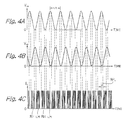
Figs. 4A, 4B and 4C are timing diagrams for explaining the horizontal scanning operation of the MEMS optical deflector ofFig. 1 ; -
Figs. 5A, 5B and 5C are timing diagrams for explaining the vertical scanning operation of the MEMS optical deflector ofFig. 1 ; -
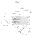
Fig. 6 is a diagram showing the relationship between a scanning locus of the MEMS optical deflector and a projected view field of the laser beam of the laser light source ofFig. 1 ; -
Fig. 7 is a functional block diagram of the drive voltage generating section and the drive voltage processing section for the vertical scanning operation of the MEMS optical deflector ofFig. 1 ; -
Fig. 8 is a flowchart of software carrying out the same operation as the operation of the adder and the PID controller ofFig. 7 ; -
Fig. 9 is a flowchart of software carrying out the same operation as the operation of the integral block and the DC offset characteristic voltage calculating block ofFig. 7 ; -
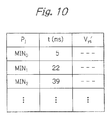
Fig. 10 is a table for storing the minimum points of the integral voltage of the same voltage ofFig. 9 ; -
Figs. 11A, 11B and 11C are timing diagrams for explaining examples of the DC offset characteristic voltage ofFigs. 7 and9 ; and -
Fig. 12 is a timing diagram illustrating a relationship among the sense voltage, the integral voltage of the sense voltage, and the vertical drive voltage ofFig. 1 . - In
Fig. 1 , which illustrates an embodiment of the apparatus according to the presently disclosed subject matter, avideo projection apparatus 1 receives a video signal VS from a video source such as a personal computer or a camera system to generate a laser beam L for ascreen 2. - The
video projection apparatus 1 is constructed by a videosignal input unit 11, a videosignal processing section 12, aframe memory 13 and acontrol section 14 for controlling the videosignal processing section 12 and theframe memory 13. - The video
signal input unit 11 is an analog red/green/blue (RGB) receiver or a digital video signal receiver such as a digital video interface (DVI), or a high-definition multimedia interface (HDMI). Video signals received by the videosignal input unit 11 are processed by a videosignal processing section 12 and are stored in theframe memory 13 frame by frame. For example, 60 frames per second are stored in theframe memory 13. Theframe memory 13 is formed by a high-speed random access memory (RAM) such as an SDRAM, a DDR2 SDRAM or a DDR3 SDRAM. In this case, one frame of theframe memory 13 corresponds to a view field formed by a horizontal angle of 40° and a vertical angle of 25° (see:Fig. 6 ). - Also, the
video projection apparatus 1 is constructed by a drivevoltage generating section 15, a drivevoltage processing section 16, and a pixeldata extracting section 17. - The drive
voltage generating section 15 generates digital drive voltages Vxa and Vya which are transmitted via adrive unit 18 formed by digital-to-analog (D/A)converters 181 and 182,amplifiers inverters optical deflector 19. In this case, analog drive voltages Vxa and Vya and their inverted drive voltages Vxb and Vyb are supplied from thedrive unit 18 to the MEMSoptical deflector 19. Note that the analog drive voltages Vya and Vyb are represented by the same denotations of the digital drive voltages Vya and Vyb, in order to simplify the description. On the other hand, the MEMSoptical deflector 19 generates sense voltages Uxsa, Vxsb, Vysa and Vysb in response to the flexing angles of the mirror thereof which are supplied via a sensevoltage input unit 20 formed by asubtracter 201, an adder 202, a band-pass filter 203, a low-pass filter 204, and analog-to-digital (A/D)converters 205 and 206 to the drivevoltage processing section 16. In this case, the band-pass filter 203 removes external noises from the sense voltage Vxs (=Vxsa-Vysb) of thesubtracter 201, while the low-pass filter 204 removes external noises from the sense voltage Vys (=Vysa+Vysb) of the adder 202. The A/D converter 205 performs an A/D conversion upon the output voltage of the band-pass filter 203 to transmit a digital sense voltage Vxs to the drivevoltage processing section 16, while the A/D converter 206 performs an A/D conversion upon the output voltage of the low-pass filter 204 to transmit a digital sense voltage Vys to the drivevoltage processing section 16. Note that the digital sense voltages Vys and Vys are represented by the same denotations of the analog output voltages Vys and Vys of thesubtracter 201 and the adder 202, in order to simplify the description. - The pixel
data extracting section 17 generates a drive voltage which is supplied to a lightsource drive unit 21 formed by a D/A converter 211 and anamplifier 212 for supplying a drive current Id to alaser light source 22. Note that the lightsource drive unit 21 and thelaser light source 22 can be provided for each of red (R), green (G) and blue (B). Also, thelaser light source 22 can be replaced by a light emitting diode (LED) source. - The drive
voltage generating section 15, the drivevoltage processing section 16 and the pixeldata extracting section 17 are controlled by thecontrol section 14. - In more detail, the drive
voltage generating section 15 transmits extracting timing signals of pixel data to the pixeldata extracting section 17. Also, the drivevoltage processing section 16 receives drive voltages similar to the drive voltages Vxa and Vya from the drivevoltage generating section 15 and the sense voltages Vxs and Vys from the sensevoltage input unit 20 to transmit a delay timing signal to the pixeldata extracting section 17 due to the delay transmission of the drive voltages Vxa and Vya to the mirror of the MEMSoptical deflector 19. Further, the pixeldata extracting section 17 extracts pixel data from theframe memory 13 in accordance with the extracting timing signals of the drivevoltage generating section 15 and the delay signal of the drivevoltage processing section 16. - In
Fig. 1 , the videosignal processing section 12, thecontrol section 14, the drivevoltage generating section 15, the drivevoltage processing section 16 and the pixeldata extracting section 17 can be formed by asingle control unit 23 or a microcomputer using a field-programmable gate array (FPGA), an extensible processing platform (EPP) or a system-on-a-chip (SoC). Thecontrol section 14 has an interface function with a universal asynchronous receiver transmitter (UART) and the like. - In
Fig. 2 , which is a perspective view of the MEMSoptical deflector 19 ofFig. 1 , the MEMSoptical deflector 19 is constructed by acircular mirror 191 for reflecting incident light L from thelaser light source 22, an inner frame (movable frame) 192 surrounding themirror 191 for supporting themirror 191, a pair oftorsion bars mirror 191 and theinner frame 192, a pair of innerpiezoelectric actuators inner frame 192 and themirror 191 and serving as cantilevers for rocking themirror 191 with respect to an X-axis of themirror 191, an outer frame (support frame) 195 surrounding theinner frame 192, a pair of meander-type outerpiezoelectric actuators outer frame 195 and theinner frame 192 and serving as cantilevers for rocking themirror 191 through theinner frame 192 with respect to a Y-axis of themirror 191 perpendicular to the X-axis,piezoelectric sensors piezoelectric sensors torsion bar 194b, andpiezoelectric sensors inner frame 192 in the proximity of the outerpiezoelectric actuators - The
inner frame 192 is rectangularly-framed to surround themirror 191 associated with the innerpiezoelectric actuators - The
torsion bars inner frame 192 and other ends coupled to the outer circumference of themirror 191. Therefore, thetorsion bars piezoelectric actuators mirror 191 with respect to the X-axis. - The inner
piezoelectric actuators torsion bars piezoelectric actuators inner frame 192 and other ends coupled to thetorsion bars piezoelectric actuator 193a is opposite to that of the innerpiezoelectric actuator 193b. - The
outer frame 195 is rectangularly-framed to surround theinner frame 192 via the outerpiezoelectric actuators - The outer
piezoelectric actuators outer frame 195 and the outer circumference of theinner frame 192, in order to rock theinner frame 192 associated with themirror 191 with respect to theouter frame 195, i.e., to rock themirror 191 with respect to the Y-axis. - The outer
piezoelectric actuator 196a is constructed bypiezoelectric cantilevers 196a-1, 196a-2, 196a-3 and 196a-4 which are serially-coupled from theouter frame 195 to theinner frame 192. Also, each of thepiezoelectric cantilevers 196a-1, 196a-2, 196a-3 and 196a-4 are in parallel with the X-axis of themirror 191. Therefore, thepiezoelectric cantilevers 196a-1, 196a-2, 196a-3 and 196a-4 are folded at every cantilever or meandering from theouter frame 195 to theinner frame 192, so that the amplitudes of thepiezoelectric cantilevers 196a-1, 196a-2, 196a-3 and 196a-4 can be changed along directions perpendicular to the Y-axis of themirror 191. - Similarly, the outer
piezoelectric actuator 196b is constructed bypiezoelectric cantilevers 196b-1, 196b-2, 196b-3 and 196b-4 which are serially-coupled from theouter frame 195 to theinner frame 192. Also, each of thepiezoelectric cantilevers 196b-1, 196b-2, 196b-3 and 196b-4 are in parallel with the X-axis of themirror 191. Therefore, thepiezoelectric cantilevers 196b-1, 196b-2, 196b-3 and 196b-4 are folded at every cantilever or meandering from theouter frame 195 to theinner frame 192, so that the amplitudes of thepiezoelectric cantilevers 196b-1, 196b-2, 196b-3 and 196b-4 can be changed along directions perpendicular to the Y-axis of themirror 191. - Note that the number of piezoelectric cantilevers in the outer
piezoelectric actuator 196a and the number of piezoelectric cantilevers in the outerpiezoelectric actuator 196b can be other values such as 2, 6, 8, ···. - The
piezoelectric sensors mirror 191 mainly caused by the innerpiezoelectric actuators piezoelectric sensors Fig. 1 ) between the two sense voltages Vxsa and Vxsb would cancel noises included therein. Therefore, the sense voltage Vxs (=Vxsa - Vxsb) of thesubtracter 201 of the sensevoltage input unit 20 ofFig. 1 is a representative sense deflecting angle signal caused the innerpiezoelectric actuators piezoelectric sensors - The
piezoelectric sensors mirror 191 mainly caused by the outerpiezoelectric actuators piezoelectric sensors voltage input unit 20 ofFig. 1 is a representative sense deflecting angle signal caused the outerpiezoelectric actuators piezoelectric sensors - The structure of each element of the MEMS
optical deflector 19 is explained below. - The
mirror 191 is constructed by a monocrystalline silicon support layer serving as a vibration plate and a metal layer serving as a reflector. - The
inner frame 192, thetorsion bars outer frame 195 are constructed by the monocrystalline silicon support layer and the like. - Each of the
piezoelectric actuators piezoelectric cantilevers 196a-1 to 196a-4 and 196b-1 to 196b-4 and thepiezoelectric sensors - The meander-
type piezoelectric actuators - In the
piezoelectric actuators piezoelectric cantilevers 196a-1, 196a-2, 196a-3, 196a-4, 196b-1 196b-2, 196b-3 and 196b-4 are divided into an odd-numbered group of thepiezoelectric cantilevers 196a-1 and 196a-3; 196b-1 and 196b-3, and an even-numbered group of thepiezoelectric cantilevers 196a-2 and 196a-4; 196b-2 and 196b-4 alternating with the odd-numbered group of thepiezoelectric cantilevers 196a-1 and 196a-3; 196b-1 and 196b-3. -
Figs. 3A and 3B are perspective views for explaining the operation of the piezoelectric cantilevers of one outer piezoelectric actuator such as 196a ofFig. 2 . Note thatFig. 3A illustrates a non-operation state of thepiezoelectric cantilevers 196a-1, 196a-2, 196a-3 and 196a-4 of thepiezoelectric actuator 196a, andFig. 3B illustrates an operation state of thepiezoelectric cantilevers 196a-1, 196a-2, 196a-3 and 196a-4 of the outerpiezoelectric actuator 196a. - As illustrated in
Fig. 3B which illustrates only thepiezoelectric cantilevers 196a-1, 196a-2, 196a-3 and 196a-4, when the odd-numbered group of thepiezoelectric cantilevers 196a-1, 196a-3, 196b-1 and 196b-3 are flexed in one direction, for example, in a downward direction D, the even-numbered group of thepiezoelectric cantilevers 196a-2, 196a-4, 196b-2 and 196b-4 are flexed in the other direction, i.e., in an upward direction U. On the other hand, when the odd-numbered group of thepiezoelectric cantilevers 196a-1, 196a-3, 196b-1 and 196b-3 are flexed in the upward direction, the even-numbered group of thepiezoelectric cantilevers 196a-2, 196a-4, 196b-2 and 196b-4 are flexed in the downward direction D. - Thus, the
mirror 191 is rocked with respect to the Y-axis. - First, a main scanning operation or horizontal scanning operation by rocking the
mirror 191 with respect to the X-axis is explained in detail with reference toFigs. 4A, 4B and 4C . - As illustrated in
Figs. 4A and 4B , the drive voltage Vxa and the drive voltage Uxv generated from thedrive unit 18 are sinusoidal at a relatively high resonant frequency fx and symmetrical or opposite in phase to each other. As a result, the innerpiezoelectric actuators torsion bars mirror 191 with respect to the X-axis. - In the above-mentioned horizontal scanning operation, the changing rates of the drive voltages Vxa and Vxb are low at their lowest and highest levels as illustrated in
Figs. 4A and 4B , so that the brightness thereof at thescreen 2 would be particularly high. Therefore, as illustrated inFig. 4C , horizontal blanking periods BPx for turning off thelaser light source 22 are provided where the changing rates of the drive voltages Vxa and Vxb are low to make the brightness at theentire screen 2 uniform. Additionally, right-direction horizontal scanning periods RH alternating with left-direction horizontal scanning periods LH are provided between the horizontal blanking periods BPx, in order to increase the depicting time period, and thus the depicting efficiency can be enhanced. - Next, a sub scanning operation or vertical scanning operation by rocking the
mirror 191 with respect to the Y-axis is explained in detail with reference toFigs. 5A, 5B and 5C . - As illustrated in
Figs. 5A and 5B , the drive voltage Vya and the drive voltage Vyb are saw-tooth-shaped at a relatively low non-resonant frequency fY and symmetrical or opposite in phase to each other. As a result, thepiezoelectric cantilevers 196a-1, 196a-3, 196b-1 and 196b-3 and thepiezoelectric cantilevers 196a-2, 196a-4, 196b-2 and 196b-4 carry out flexing operations in opposite directions to each other, so that themirror 191 is rocked with respect to the Y-axis. - In the above-mentioned vertical scanning operation, the changing rate of the drive voltages Vya and Vyb are low at their lowest and highest levels as illustrated in
Figs. 5A and 5B , so that the brightness thereof at thescreen 2 would be particularly high. Therefore, as illustrated inFig. 5C , vertical blanking periods BPY for turning off thelaser light source 22 are provided where the changing rates of the drive voltages Vya and Vyb are low to make the brightness at theentire screen 2 uniform. - As illustrated in
Fig. 6 , which is a diagram illustrating a relationship between a scanning locus SL of the MEMSoptical deflector 19 and a projected area of the laser beam L of thelaser light source 22 ofFig. 1 , a horizontal scanning line H and a vertical scanning line V by the MEMSoptical deflector 19 are protruded from a projected view field F of the laser beam L defined by a horizontal angle of 40° , for example, and a vertical angle of 25° , for example. - In the horizontal scanning operation, the drive
voltage generating section 15 includes a sinusoidal-wave voltage generating block (not shown) for generating a sinusoidal-wave voltage Vya and a phase-locked loop block (not shown) for transmitting the sinusoidal-wave voltage Vya to thedrive unit 18. When the drivevoltage processing section 16 receives the sense voltage Vxs from the sensevoltage input unit 20, to calculate an integral voltage Vxs' of the sense voltage Vxs, the integral voltage Vxs' is transmitted to the drivevoltage generating section 15, so that the phase-locked loop block generates the sinusoidal-wave voltage Vxa phase-locked to the integral voltage Vxs'. - The vertical scanning operation is explained in more detail with reference to
Fig. 7 , which is a functional block circuit diagram of the drivevoltage generating section 15 and the drivevoltage processing section 16 ofFig. 1 . - In
Fig. 7 , the drivevoltage generating section 15 is constructed by a saw-toothvoltage generating block 151 operated by thecontrol section 14, asubtracter block 152, and a proportional/integral/derivative (PID)controller 153 formed by aproportional block 1531, anintegral block 1532, a derivative block 1583, and anadder block 1534. On the other hand, the drivevoltage processing section 16 is constructed by a sum (or integral) block 161 and a DC offset characteristicvoltage calculating block 162 for calculating a DC offset characteristic voltage C used in theintegral block 161. - In the drive
voltage generating section 15 ofFig. 7 , thesubtracter 152 calculates a deviation e(t) by
- where Vy is a saw-tooth voltage generated from the saw-tooth
voltage generating block 151; and - Vys' is the output voltage (sum voltage or integral voltage) of the
integral block 161 of the drivevoltage processing section 16. ThePID controller 153 is operated to generate the drive voltage Vya so that the deviation e (t) is brought close to zero, i. e. , the integral voltage Vys' of theintegral block 161 of the drivevoltage processing section 16 is brought close to the saw-tooth voltage Vy. In more detail, theproportional block 1531 calculates a proportional term up=Kpe(t), theintegral block 1532 calculates an integral term ui=Ki ∫e(t) dt, thederivative block 1533 calculates a derivative term ud=Kdd(e(t))/dt, and theadder block 1534 calculates a vertical drive voltage Vya=un+ui+ud. In this case, a proportion gain Kp, an integral gain Ki and a derivative gain Kd are predetermined to have optimum values. - Note that the
PID controller 153 can be another controller which includes only theproportional block 1531 and theintegral block 1532, for example. - In the drive
voltage processing section 16, theintegral block 161 calculates an integral voltage Vys' of the sense voltage Vys by
piezoelectric sensors - The DC offset characteristic voltage C is calculated by the DC offset characteristic
voltage calculating block 162 using a gradient of the integral voltage Vys' with respect to time. Note that the DC offset characteristic voltage C is initialized at 0. - The inventor has found that the gradient of the integral voltage Vys' represents a DC offset voltage generated in the sense voltage Vys (=Vysa+Vysb) of the
piezoelectric sensors - The DC offset characteristic
voltage calculating block 162 is constructed by a minimumpoint calculating block 1621 for calculating minimum points MIN0, MIN1, MIN2, ··· on the integral voltage Vys'. For example, such minimum points MIN0, MIN1, MIN2, ···, can be detected by differentiating the integral voltage Vys' with respect to time, that is, rising points as minimum points can be detected in the differentiated integral voltage Vys'. As a result, minimum points MIN0, MIN1, MIN2, ··· are obtained (see:Figs. 11A, 11B and 11C ). Also, the DC offset characteristicvoltage calculating block 162 is constructed by a straight line calculating block 163 which calculates a straight line designated by Vys'=A·t+B approximate to the minimum points MIN0, MIN1, MIN2, ··· using the least square method. Note that A is a gradient of the straight line with respect to time. Further, the DC offset characteristicvoltage calculating block 162 is constructed by a DC offset characteristicvoltage setting block 1623 which sets the DC offset characteristic voltage C by
- In
Fig. 7 , the minimumpoint calculating block 1621 can be replaced by a maximum point calculating block which calculates maximum points MAX0, MAX1, MAX2, (seeFigs. 11A, 11B and 11C ). The maximum points MAX0, MAX1, MAX1, ··· have a gradient tendency the same as that of the minimum points MIN0, MIN1, MIN2, ···. Therefore, in this case, the straightline calculating block 1622 can calculate the same straight line using the maximum points MAX0, MAX1, MAX2, ···. - The operation of the
adder 152 and thePID controller 153 ofFig.7 can be carried out by software illustrated by a flowchart inFig. 8 executed at every time period T ms such as 1ms. - First, at
step 801, a deviation "e" is calculated by
- where Vy is a saw-tooth voltage generated from the saw-tooth
voltage generating block 151; and - Vys' is an integral voltage of the
integral block 161 of the drivevoltage processing section 16. - Next, at
step 802, a proportional term up is calculated by
- Next, at
step 803, an integral term ui is calculated by
- Then, the previous integral term uio is replaced by the current integral term ui at
step 804. - Next, at
step 805, a derivative term ud is calculated by
- where Kd is a derivative gain; and
- e0 is a previous deviation.
- Then, the previous deviation e0 is replaced by the current deviation "e" at
step 806. - Next, at
step 807, a vertical drive voltage Vya is calculated by
- Next, at
step 808, the vertical drive voltage Vya is transmitted to thedrive unit 18. - The flowchart of
Fig. 8 is completed by step 809. - The operation of the
integral block 161 and the DC offset characteristicvoltage calculating block 162 ofFig. 7 can be carried out by software illustrated by a flowchart inFig. 9 executed at every time period T ms such as 1 ms. Note that a DC offset characteristic voltage C is initialized at 0. Also, counters "i" and "j" are initialized at 0. - First, at step 901, the counter "i" is counted up by +1.
- Next, at
step 902, it is determined whether or not i<im is satisfied. Note that im is 500 corresponding to 500 ms, for example. As a result, if i≧im, the control proceeds tosteps 903 through 906 which calculate the DC offset characteristic voltage C, while if i<im, the control proceeds directly to step 907. -
Steps 903 through 906 are explained later. - At
step 907, the integral voltage Vys' is renewed by
- Next, at
step 908, it is determined whether or not i≧3 is satisfied. As a result, if i≧3, the control proceeds to step 909. Otherwise, i.e., if i<3, the control proceeds directly to step 912. - At
step 909, it is determined whether or not the following formula is satisfied:
- where Vys1' is a previous voltage of the integral voltage Vys'; and
- Vys2' is a second-previous voltage of the integral voltage Vys'. That is, it is determined whether or not the previous sampling point ((i-1)T, Vys1') is a minimum point of the integral voltage Vys'. As a result, if ((i-1)T, Vys1') is a minimum point Pj, the control proceeds to step 910. Otherwise, the control proceeds directly to step 912. At step 910, Pj=((i-1)T, Vys1') is stored in a minimum point table as illustrated in
Fig. 10 . Then, the counter j is counted up by +1 atstep 911. -
Steps 903 to 906 are explained below. - At
step 903, a straight line represented by Vys'=A. t+B approximate to the minimum points Pj stored in the minimum point table is obtained by a least square method. Note that A is a gradient of the straight line with respect to time. - Next, at
step 904, a DC offset characteristic voltage C is calculated by
- Then, the counter "i" is initialized at 0 by
step 905, and the counter "j" is initialized at 0 bystep 906. - Also, at
step 912, the second-previous integral voltage Vys2' is replaced by the previous integral voltage Vys1', and atstep 913, the previous integral voltage Vys1' is replaced by the current integral voltage Vys'. - Thus, the flowchart of
Fig. 9 is completed bystep 914. - Note that, at
step 909, it can be determined whether or not the following formula is satisfied:
- That is, it can be determined whether or not the previous sampling point ((i-1)T, Vys1') is a maximum point of the integral voltage Vys'. As a result, if ((i-1)T, Vys1') is a maximum point Pj, the control proceeds to step 910 which stores Pj=((i-1)T, Vys1') in a maximum point table similar to the minimum point table of
Fig. 10 . - As illustrated in
Fig. 11A , when the sense voltage Vys (=Vysa+Vysb) has no DC offset voltage relative to a reference level REF, the mean value of the integral voltage Vys' is unchanged. As a result, a straight line approximate to the minimum points MIN0, MIN1, MIN2, ··· (the maximum points MAX0, MAX1, MAX2, ···) is horizontal. Therefore, the DC offset characteristic voltage C is approximately 0. - Also, as illustrated in
Fig. 11B , when the sense voltage Vys (=Vysa+Vysb) has a positive DC offset voltage relative to the reference level REF, the mean value of the integral voltage Vys' is changing downward. As a result, a straight line approximate to the minimum points MIN0, MIN1, MIN2, ··· (the maximum points MAX0, MAX1, MAX2, ···) is sloped downward. Therefore, the DC offset characteristic voltage C is negative. - Further, as illustrated in
Fig. 11C , when the sense voltage Vys (=Vysa+Vysb) has a negative DC offset voltage relative to the reference level REF, the mean value of the integral voltage Vys' is changing upward. As a result, a straight line approximate to the minimum points MIN2, MIN1, MIN2, ··· (the maximum points MAX0 MAX1, MAX1, ···) is sloped upward. Therefore, the DC offset characteristic voltage C is positive. - According to the inventor's experiment, the analog sense voltage Vys (=Vysa+Vysb) of the adder 202, the integral voltage Vys' of the
integral block 161 and the vertical drive voltage Vya illustrated inFig. 12 were obtained under the condition that themirror 191 has a diameter of 1.2 mm and a thickness of 45 µ m. That is, inFig. 12 , the integral voltage Vys' could completely follow the vertical drive voltage Vya. As a result, even when a DC offset voltage was generated in thepiezoelectric sensors mirror 191 could accurately be controlled. - In
Fig. 2 , note that the innerpiezoelectric actuators torsion bars - It will be apparent to those skilled in the art that various modifications and variations can be made in the presently disclosed subject matter without departing from the spirit or scope of the presently disclosed subject matter. Thus, it is intended that the presently disclosed subject matter covers the modifications and variations of the presently disclosed subject matter provided they come within the scope of the appended claims and their equivalents. All related or prior art references described above and in the Background section of the present specification are hereby incorporated in their entirety by reference.
Claims (14)
- An apparatus including an optical deflector (19) and a control unit (23) for controlling said optical deflector (19), wherein said optical deflector (19) comprises:a mirror (191);a piezoelectric actuator (196a, 196b) adapted to rock said mirror (191) around an axis of said mirror (191); anda piezoelectric sensor (198a, 198b) adapted to sense vibrations of said piezoelectric actuator (196a, 196b),wherein said control unit (23) comprises:a saw-tooth voltage generating block (151) adapted to generate a saw-tooth voltage (Vy);an integral block (161) adapted to calculate an integral voltage (Vys') of a sum of a sense voltage (Vys) of said piezoelectric sensor (198a, 198b) and a DC offset characteristic voltage (C);a DC offset characteristic voltage calculating block (162) adapted to calculate said DC offset characteristic voltage (C) in accordance with said integral voltage (Vys');a subtracter block (152), connected to said saw tooth voltage generating block and said integral block (161) and adapted to generate a deviation (e(t)) between said saw-tooth voltage (Vy) and said integral voltage (Vys'); anda controller (153), connected to said subtracter block (152) and adapted to generate a drive voltage (Vya) in accordance with said deviation (e(t)) to apply said drive voltage (Vya) to said piezoelectric actuator (196a, 196b).
- The apparatus set forth in claim 1, wherein said DC offset characteristic voltage calculating block (162) comprises:a minimum point calculating block (1621) adapted to calculate minimum points (MIN0, MIN1, MIN2, ···) of said integral voltage (Vys');a straight line calculating block (1622), connected to said minimum point calculating block (1621) and adapted to calculate a straight line approximate to said minimum points (MIN0, MIN1, MIN2, ··· ); anda DC offset characteristic voltage setting block (1623) connected to said straight line calculating block (1622) and adapted to set said DC offset characteristic voltage (C) in accordance with a gradient (A) of said straight line with respect to time.
- The apparatus as set forth in claim 2, wherein said DC offset characteristic voltage setting block (1623) sets said DC offset characteristic voltage C by
 where A is the gradient of said straight line with respect to time; andα is a constant larger than 1.
 - The apparatus set forth in claim 1, wherein said DC offset characteristic voltage calculating block (162) comprises:a maximum point calculating block adapted to calculate maximum points (MAX0, MAX1, MAX1, ··· of said integral voltage (Vys');a straight line calculating block, connected to said maximum point calculating block and adapted to calculate a straight line approximate to said maximum points (MAX0, MAX1, MAX1, ···); anda DC offset characteristic voltage setting block (1623) connected to said straight line calculating block (1622) and adapted to set said DC offset characteristic voltage (C) in accordance with a gradient (A) of said straight line with respect to time.
- The apparatus as set forth in claim 4, wherein said DC offset characteristic voltage setting block (1623) sets said DC offset characteristic voltage C by
 where A is the gradient of said straight line with respect to time; andα is a constant larger than 1.
 - The apparatus set forth in claim 1, wherein said controller (153) comprises a proportional/integral/derivative (PID) controller (153).
- The apparatus as set forth in claim 1, further comprising a light source (22), said control unit controlling said light source (22) to reflect light from said light source (22) to project a view field.
- A method for controlling an optical deflector (19) including: a mirror (191); a piezoelectric actuator (196a, 196b) adapted to rock said mirror (191) around an axis of said mirror (191); and a piezoelectric sensor (198a, 198b) adapted to sense vibrations of said piezoelectric actuator (196a, 196b),
said method comprising:generating a saw-tooth voltage (Vy);calculating an integral voltage (Vys') of a sum of a sense voltage (Vys) of said piezoelectric sensor (198a, 198b) and a DC offset characteristic voltage (C);calculating said DC offset characteristic voltage (C) in accordance with said integral voltage (Vys');generating a deviation (e(t)) between said saw-tooth voltage (Vy) and said integral voltage (Vys'); andgenerating a drive voltage (Vya) in accordance with said deviation (e(t)) to apply said drive voltage (Vya) to said piezoelectric actuator (196a, 196b). - The method set forth in claim 8, wherein said DC offset characteristic voltage calculating comprising:calculating minimum points (MIN0, MIN1, MIN2, ···) of said integral voltage (Vys');calculating a straight line approximate to said minimum points (MIN0, MIN1, MIN2, ···); andsetting said DC offset characteristic voltage (C) in accordance with a gradient (A) of said straight line with respect to time.
- The method as set forth in claim 9, wherein said DC offset characteristic voltage setting sets said DC offset characteristic voltage C by
 where A is the gradient of said straight line with respect to time; andα is a constant larger than 1.
 - The method set forth in claim 8, wherein said DC offset characteristic voltage calculating comprises:calculating maximum points (MAX0, MAX1, MAX2, ···) of said integral voltage (Vys');calculating a straight line approximate to said maximum points (MAX0, MAX1, MAX2, ···); andsetting said DC offset characteristic voltage (C) in accordance with a gradient (A) of said straight line with respect to time.
- The method as set forth in claim 11, wherein said DC offset characteristic voltage setting sets said DC offset characteristic voltage C by
 where A is the gradient of said straight line with respect to time; andα is a constant larger than 1.
 - The method set forth in claim 8, wherein said controlling comprises proportional/integral/derivative (PID) controlling.
- The method as set forth in claim 8, further controlling a light source (22) to reflect light from said light source (22) to project a view field.
Applications Claiming Priority (1)
| Application Number | Priority Date | Filing Date | Title |
|---|---|---|---|
| JP2015025221A JP2016148763A (en) | 2015-02-12 | 2015-02-12 | Picture projection device |
Publications (1)
| Publication Number | Publication Date |
|---|---|
| EP3056936A1 true EP3056936A1 (en) | 2016-08-17 |
Family
ID=55524074
Family Applications (1)
| Application Number | Title | Priority Date | Filing Date |
|---|---|---|---|
| EP16155111.4A Withdrawn EP3056936A1 (en) | 2015-02-12 | 2016-02-10 | Apparatus including optical deflector controlled by saw-tooth voltage and its controlling method |
Country Status (3)
| Country | Link |
|---|---|
| US (1) | US20160238835A1 (en) |
| EP (1) | EP3056936A1 (en) |
| JP (1) | JP2016148763A (en) |
Cited By (2)
| Publication number | Priority date | Publication date | Assignee | Title |
|---|---|---|---|---|
| CN109946828A (en) * | 2017-12-21 | 2019-06-28 | 三美电机株式会社 | Light scanning apparatus |
| EP4009312A1 (en) * | 2020-12-02 | 2022-06-08 | STMicroelectronics S.r.l. | Closed-loop position control of mems micromirrors |
Families Citing this family (9)
| Publication number | Priority date | Publication date | Assignee | Title |
|---|---|---|---|---|
| US10491866B2 (en) * | 2015-08-26 | 2019-11-26 | Ricoh Company, Ltd. | Actuator controlling device, drive system, video device, image projection device, and actuator controlling method |
| JP2018081176A (en) * | 2016-11-15 | 2018-05-24 | 株式会社デンソー | MEMS device |
| CN107688291A (en) * | 2017-08-23 | 2018-02-13 | 苏州大学 | The feedforward of piezoelectric ceramics platform and closed loop composite control method, system based on single neuron |
| CN107608209A (en) * | 2017-08-23 | 2018-01-19 | 苏州大学 | The feedforward of piezoelectric ceramic actuator and closed loop composite control method, system |
| CN107479379A (en) * | 2017-08-23 | 2017-12-15 | 苏州大学 | Piezoelectricity pottery driver feedforward and closed loop composite control method, system based on genetic algorithm |
| US11221478B2 (en) | 2019-04-15 | 2022-01-11 | Microsoft Technology Licensing, Llc | MEMS scanner |
| US11039111B2 (en) | 2019-05-23 | 2021-06-15 | Microsoft Technology Licensing, Llc | MEMS control method to provide trajectory control |
| US11108735B2 (en) | 2019-06-07 | 2021-08-31 | Microsoft Technology Licensing, Llc | Mapping subnets in different virtual networks using private address space |
| JP7338403B2 (en) * | 2019-10-30 | 2023-09-05 | 株式会社リコー | Optical deflectors, image projection devices, head-up displays, laser headlamps, head-mounted displays, object recognition devices, and vehicles |
Citations (6)
| Publication number | Priority date | Publication date | Assignee | Title |
|---|---|---|---|---|
| EP1719012A2 (en) * | 2004-02-09 | 2006-11-08 | Microvision, Inc. | Mems scanning system with improved performance |
| US20100073748A1 (en) | 2008-09-22 | 2010-03-25 | Microvision, Inc. | Scanning Mirror Control |
| US20120224239A1 (en) * | 2011-03-04 | 2012-09-06 | Stanley Electric Co., Ltd. | Driver for optical deflector using two asyncronous saw-tooth drive voltages and method for setting the same |
| US20120242191A1 (en) * | 2011-03-22 | 2012-09-27 | Stanley Electric Co., Ltd. | Driver for optical deflector using two modified syncronous saw-tooth drive voltages and method for setting the same |
| US20130258432A1 (en) * | 2012-03-29 | 2013-10-03 | Stanley Electric Co., Ltd. | Optical deflector |
| US8730540B2 (en) | 2011-04-04 | 2014-05-20 | Nisca Corporation | Sheet transport apparatus |
Family Cites Families (1)
| Publication number | Priority date | Publication date | Assignee | Title |
|---|---|---|---|---|
| JP5252389B2 (en) * | 2005-12-20 | 2013-07-31 | 国立大学法人金沢大学 | Scanning probe microscope |
-
2015
- 2015-02-12 JP JP2015025221A patent/JP2016148763A/en active Pending
-
2016
- 2016-01-20 US US15/002,210 patent/US20160238835A1/en not_active Abandoned
- 2016-02-10 EP EP16155111.4A patent/EP3056936A1/en not_active Withdrawn
Patent Citations (7)
| Publication number | Priority date | Publication date | Assignee | Title |
|---|---|---|---|---|
| EP1719012A2 (en) * | 2004-02-09 | 2006-11-08 | Microvision, Inc. | Mems scanning system with improved performance |
| US20100073748A1 (en) | 2008-09-22 | 2010-03-25 | Microvision, Inc. | Scanning Mirror Control |
| JP5543468B2 (en) | 2008-09-22 | 2014-07-09 | マイクロビジョン,インク. | Scanning mirror control |
| US20120224239A1 (en) * | 2011-03-04 | 2012-09-06 | Stanley Electric Co., Ltd. | Driver for optical deflector using two asyncronous saw-tooth drive voltages and method for setting the same |
| US20120242191A1 (en) * | 2011-03-22 | 2012-09-27 | Stanley Electric Co., Ltd. | Driver for optical deflector using two modified syncronous saw-tooth drive voltages and method for setting the same |
| US8730540B2 (en) | 2011-04-04 | 2014-05-20 | Nisca Corporation | Sheet transport apparatus |
| US20130258432A1 (en) * | 2012-03-29 | 2013-10-03 | Stanley Electric Co., Ltd. | Optical deflector |
Cited By (4)
| Publication number | Priority date | Publication date | Assignee | Title |
|---|---|---|---|---|
| CN109946828A (en) * | 2017-12-21 | 2019-06-28 | 三美电机株式会社 | Light scanning apparatus |
| CN109946828B (en) * | 2017-12-21 | 2022-04-26 | 三美电机株式会社 | Optical scanning device |
| EP4009312A1 (en) * | 2020-12-02 | 2022-06-08 | STMicroelectronics S.r.l. | Closed-loop position control of mems micromirrors |
| US11841497B2 (en) | 2020-12-02 | 2023-12-12 | Politecnico Di Milano | Closed-loop position control of MEMS micromirrors |
Also Published As
| Publication number | Publication date |
|---|---|
| JP2016148763A (en) | 2016-08-18 |
| US20160238835A1 (en) | 2016-08-18 |
Similar Documents
| Publication | Publication Date | Title |
|---|---|---|
| US20160238835A1 (en) | Apparatus including optical deflector controlled by saw-tooth voltage and its controlling method | |
| EP3012823B1 (en) | Video projection apparatus capable of operating at optimum resonant frequency and its controlling method | |
| US10080001B2 (en) | Video projection apparatus capable of realizing stable rocking angle at optimum resonant frequency | |
| US9291817B2 (en) | Optical deflection device, apparatus including the same, and method of controlling optical deflecting device | |
| JP5151065B2 (en) | Optical scanner and scanning projector | |
| US10018833B2 (en) | MEMS device and electronic device having projector function | |
| JP5397184B2 (en) | Two-dimensional optical scanner drive device | |
| JP6641709B2 (en) | Optical deflection device, image forming device, image display device, moving body device, and adjustment method for optical deflection device | |
| EP2711916A1 (en) | Trapezoidal distortion correction in a laser projection apparatus | |
| JP2012145755A (en) | Image display device | |
| EP3086548A1 (en) | Image display device and control method for same | |
| Ikegami et al. | A biaxial piezoelectric MEMS scanning mirror and its application to pico-projectors | |
| EP2911380A1 (en) | Inclining action device, optical scanner employing the inclining action device, and image displaying apparatus employing the inclining action device | |
| JP6946708B2 (en) | Control device, image projection device, and control method | |
| US20200201028A1 (en) | Light deflection device, image projector, laser head lamp, and mobile object | |
| JP7027689B2 (en) | Light deflector and image projection device | |
| US9414034B2 (en) | Video projection system including multiple local video projection units | |
| JP2013003526A (en) | Optical scanning device | |
| JP2015040928A (en) | Optical deflection apparatus, image forming apparatus, vehicle, and control method of optical deflection apparatus | |
| US9664900B2 (en) | Projection apparatus and projection method | |
| EP3136153B1 (en) | Actuator controlling device, drive system, video device, image projection device, and actuator controlling method | |
| JP2013160953A (en) | Oscillating device, optical scanner using the same, image display device and control method of oscillating device | |
| JP7396147B2 (en) | Movable devices, optical deflection devices, image projection devices, optical writing devices, object recognition devices, moving objects, head-mounted displays | |
| US20250306380A1 (en) | Image generation device | |
| JP4998291B2 (en) | Optical scanning device |
Legal Events
| Date | Code | Title | Description |
|---|---|---|---|
| PUAI | Public reference made under article 153(3) epc to a published international application that has entered the european phase |
Free format text: ORIGINAL CODE: 0009012 |
|
| AK | Designated contracting states |
Kind code of ref document: A1 Designated state(s): AL AT BE BG CH CY CZ DE DK EE ES FI FR GB GR HR HU IE IS IT LI LT LU LV MC MK MT NL NO PL PT RO RS SE SI SK SM TR |
|
| AX | Request for extension of the european patent |
Extension state: BA ME |
|
| 17P | Request for examination filed |
Effective date: 20170213 |
|
| RBV | Designated contracting states (corrected) |
Designated state(s): AL AT BE BG CH CY CZ DE DK EE ES FI FR GB GR HR HU IE IS IT LI LT LU LV MC MK MT NL NO PL PT RO RS SE SI SK SM TR |
|
| STAA | Information on the status of an ep patent application or granted ep patent |
Free format text: STATUS: THE APPLICATION HAS BEEN WITHDRAWN |
|
| 18W | Application withdrawn |
Effective date: 20180209 |