EP3056935B1 - Mems scanner - Google Patents
Mems scanner Download PDFInfo
- Publication number
- EP3056935B1 EP3056935B1 EP13895294.0A EP13895294A EP3056935B1 EP 3056935 B1 EP3056935 B1 EP 3056935B1 EP 13895294 A EP13895294 A EP 13895294A EP 3056935 B1 EP3056935 B1 EP 3056935B1
- Authority
- EP
- European Patent Office
- Prior art keywords
- fixed
- driving
- pair
- electrodes
- electrode portion
- Prior art date
- Legal status (The legal status is an assumption and is not a legal conclusion. Google has not performed a legal analysis and makes no representation as to the accuracy of the status listed.)
- Active
Links
Images





Classifications
-
- G—PHYSICS
- G02—OPTICS
- G02B—OPTICAL ELEMENTS, SYSTEMS OR APPARATUS
- G02B26/00—Optical devices or arrangements for the control of light using movable or deformable optical elements
- G02B26/08—Optical devices or arrangements for the control of light using movable or deformable optical elements for controlling the direction of light
- G02B26/0816—Optical devices or arrangements for the control of light using movable or deformable optical elements for controlling the direction of light by means of one or more reflecting elements
- G02B26/0833—Optical devices or arrangements for the control of light using movable or deformable optical elements for controlling the direction of light by means of one or more reflecting elements the reflecting element being a micromechanical device, e.g. a MEMS mirror, DMD
- G02B26/0841—Optical devices or arrangements for the control of light using movable or deformable optical elements for controlling the direction of light by means of one or more reflecting elements the reflecting element being a micromechanical device, e.g. a MEMS mirror, DMD the reflecting element being moved or deformed by electrostatic means
-
- B—PERFORMING OPERATIONS; TRANSPORTING
- B81—MICROSTRUCTURAL TECHNOLOGY
- B81B—MICROSTRUCTURAL DEVICES OR SYSTEMS, e.g. MICROMECHANICAL DEVICES
- B81B3/00—Devices comprising flexible or deformable elements, e.g. comprising elastic tongues or membranes
- B81B3/0018—Structures acting upon the moving or flexible element for transforming energy into mechanical movement or vice versa, i.e. actuators, sensors, generators
- B81B3/0021—Transducers for transforming electrical into mechanical energy or vice versa
-
- B—PERFORMING OPERATIONS; TRANSPORTING
- B81—MICROSTRUCTURAL TECHNOLOGY
- B81B—MICROSTRUCTURAL DEVICES OR SYSTEMS, e.g. MICROMECHANICAL DEVICES
- B81B3/00—Devices comprising flexible or deformable elements, e.g. comprising elastic tongues or membranes
- B81B3/0035—Constitution or structural means for controlling the movement of the flexible or deformable elements
- B81B3/004—Angular deflection
- B81B3/0048—Constitution or structural means for controlling angular deflection not provided for in groups B81B3/0043 - B81B3/0045
-
- B—PERFORMING OPERATIONS; TRANSPORTING
- B81—MICROSTRUCTURAL TECHNOLOGY
- B81B—MICROSTRUCTURAL DEVICES OR SYSTEMS, e.g. MICROMECHANICAL DEVICES
- B81B7/00—Microstructural systems ; Auxiliary parts of microstructural devices or systems
- B81B7/02—Microstructural systems ; Auxiliary parts of microstructural devices or systems containing distinct electrical or optical devices of particular relevance for their function, e.g. microelectro-mechanical systems [MEMS]
-
- B—PERFORMING OPERATIONS; TRANSPORTING
- B81—MICROSTRUCTURAL TECHNOLOGY
- B81C—PROCESSES OR APPARATUS SPECIALLY ADAPTED FOR THE MANUFACTURE OR TREATMENT OF MICROSTRUCTURAL DEVICES OR SYSTEMS
- B81C1/00—Manufacture or treatment of devices or systems in or on a substrate
- B81C1/00015—Manufacture or treatment of devices or systems in or on a substrate for manufacturing microsystems
- B81C1/00134—Manufacture or treatment of devices or systems in or on a substrate for manufacturing microsystems comprising flexible or deformable structures
-
- G—PHYSICS
- G02—OPTICS
- G02B—OPTICAL ELEMENTS, SYSTEMS OR APPARATUS
- G02B26/00—Optical devices or arrangements for the control of light using movable or deformable optical elements
- G02B26/08—Optical devices or arrangements for the control of light using movable or deformable optical elements for controlling the direction of light
- G02B26/10—Scanning systems
-
- G—PHYSICS
- G02—OPTICS
- G02B—OPTICAL ELEMENTS, SYSTEMS OR APPARATUS
- G02B26/00—Optical devices or arrangements for the control of light using movable or deformable optical elements
- G02B26/08—Optical devices or arrangements for the control of light using movable or deformable optical elements for controlling the direction of light
- G02B26/10—Scanning systems
- G02B26/105—Scanning systems with one or more pivoting mirrors or galvano-mirrors
-
- G—PHYSICS
- G03—PHOTOGRAPHY; CINEMATOGRAPHY; ANALOGOUS TECHNIQUES USING WAVES OTHER THAN OPTICAL WAVES; ELECTROGRAPHY; HOLOGRAPHY
- G03B—APPARATUS OR ARRANGEMENTS FOR TAKING PHOTOGRAPHS OR FOR PROJECTING OR VIEWING THEM; APPARATUS OR ARRANGEMENTS EMPLOYING ANALOGOUS TECHNIQUES USING WAVES OTHER THAN OPTICAL WAVES; ACCESSORIES THEREFOR
- G03B21/00—Projectors or projection-type viewers; Accessories therefor
- G03B21/005—Projectors using an electronic spatial light modulator but not peculiar thereto
- G03B21/008—Projectors using an electronic spatial light modulator but not peculiar thereto using micromirror devices
-
- H—ELECTRICITY
- H02—GENERATION; CONVERSION OR DISTRIBUTION OF ELECTRIC POWER
- H02N—ELECTRIC MACHINES NOT OTHERWISE PROVIDED FOR
- H02N1/00—Electrostatic generators or motors using a solid moving electrostatic charge carrier
- H02N1/002—Electrostatic motors
-
- H—ELECTRICITY
- H02—GENERATION; CONVERSION OR DISTRIBUTION OF ELECTRIC POWER
- H02N—ELECTRIC MACHINES NOT OTHERWISE PROVIDED FOR
- H02N1/00—Electrostatic generators or motors using a solid moving electrostatic charge carrier
- H02N1/002—Electrostatic motors
- H02N1/006—Electrostatic motors of the gap-closing type
- H02N1/008—Laterally driven motors, e.g. of the comb-drive type
-
- H—ELECTRICITY
- H04—ELECTRIC COMMUNICATION TECHNIQUE
- H04N—PICTORIAL COMMUNICATION, e.g. TELEVISION
- H04N1/00—Scanning, transmission or reproduction of documents or the like, e.g. facsimile transmission; Details thereof
- H04N1/04—Scanning arrangements, i.e. arrangements for the displacement of active reading or reproducing elements relative to the original or reproducing medium, or vice versa
- H04N1/113—Scanning arrangements, i.e. arrangements for the displacement of active reading or reproducing elements relative to the original or reproducing medium, or vice versa using oscillating or rotating mirrors
-
- H—ELECTRICITY
- H04—ELECTRIC COMMUNICATION TECHNIQUE
- H04N—PICTORIAL COMMUNICATION, e.g. TELEVISION
- H04N3/00—Scanning details of television systems; Combination thereof with generation of supply voltages
- H04N3/02—Scanning details of television systems; Combination thereof with generation of supply voltages by optical-mechanical means only
- H04N3/08—Scanning details of television systems; Combination thereof with generation of supply voltages by optical-mechanical means only having a moving reflector
-
- B—PERFORMING OPERATIONS; TRANSPORTING
- B81—MICROSTRUCTURAL TECHNOLOGY
- B81B—MICROSTRUCTURAL DEVICES OR SYSTEMS, e.g. MICROMECHANICAL DEVICES
- B81B2201/00—Specific applications of microelectromechanical systems
- B81B2201/03—Microengines and actuators
- B81B2201/033—Comb drives
-
- B—PERFORMING OPERATIONS; TRANSPORTING
- B81—MICROSTRUCTURAL TECHNOLOGY
- B81B—MICROSTRUCTURAL DEVICES OR SYSTEMS, e.g. MICROMECHANICAL DEVICES
- B81B2201/00—Specific applications of microelectromechanical systems
- B81B2201/04—Optical MEMS
Definitions
- the present invention relates to a micro electro mechanical systems (MEMS) scanner, and more particularly, to an MEMS scanner for implementing stable driving while increasing a driving angle between a fixed electrode and a driving electrode using an MEMS process.
- MEMS micro electro mechanical systems
- MEMS micro electro mechanical systems
- an optical scanner having a micro structure is drawing attention in a display field in which light incident from a light source is radiated on a predetermined screen area to implement a video or a scanning field in which light is scanned on a predetermined screen area and reflected light is received to read out image information.
- Such an optical scanner refers to one in which a reflective mirror for reflecting light, a support axis for supporting the reflective mirror, and driving means for moving the reflective mirror are implemented as a single chip.
- a comb-shaped driver has driving electrodes that are disposed in parallel on the plane of a moving structure or a stage that is a moving object, and fixed electrodes corresponding to the driving electrodes have a structure in which the fixed electrodes are alternately disposed with respect to the driving electrodes while being fixed and are disposed in parallel on the plane surface of the stage along with the driving electrodes.
- a height difference or a slope is required between the driving electrode and the fixed electrode. Since an additional process for causing one of the driving electrode and the fixed electrode to have a different height or an additional process for causing the height to be inclined after making both heights same as each other is required for the comb-shaped driver, it becomes complicated to manufacture the optical scanner.
- Methods of forming an initial angle for the driving electrode are as follows.
- a method may be employed which deposits a polymer between an upper end of a driving electrode and an upper end of a driving portion to connect the driving electrode with the driving portion, and heat-deforms the polymer to shrink the polymer, thereby inclining the driving electrode.
- Another method is to have a rotational spring subjected to plastic deformation using Joule heating while the spring is intentionally inclined to form an initial angle.
- This method in terms of the driving angle because the optical scanner can only be driven in uni-direction at the time of electrostatically driving the optical scanner.
- Yet another method is to form an initial angle using an assembly.
- an additional separate structure needs to be coupled to an optical scanner in order to form the initial angle for the driving electrode, which thus causes the manufacturing process to be complicated and the manufacturing cost to be increased.
- a volume of the optical scanner is inevitably increased due to the added structure.
- the spring of the driving portion and a hinge of the fixed electrode are structurally connected to each other, the spring of the driving portion and the driving electrode also simultaneously rotate when the fixed electrode is inclined, so that the initial angle is not formed.
- the spring of the driving portion needs to be intentionally twisted, which causes the spring of the driving portion to have a residual stress even when the optical scanner is not driven. This causes unstable driving such as fatigue failures in the long term and a poor impact resistance to occur in terms of driving the optical scanner.
- the present invention is thus directed to providing an MEMS scanner for implementing stable driving while increasing a driving angle between a fixed electrode and a driving electrode using an MEMS process.
- the present invention is also directed to providing a method capable of reducing a manufacturing cost while having an MEMS scanner small-sized by means of manufacturing process simplification.
- One aspect of the present invention provides an MEMS scanner including a lower frame, a pair of upper frames, a pair of levers, a pair of fixed electrode portions, and a driving electrode portion.
- the lower frame has cavities downward from an upper surface of the lower frame, and a through-hole is formed between the cavities.
- the pair of upper frames are attached to the upper surface of the lower frame near the cavities to form an installation space in a central portion between the upper frames.
- the pair of levers are disposed inside the respective upper frames, are attached to both sides of a bottom surface of the cavities around the through-hole, and are connected to the respective upper frames.
- the pair of fixed electrode portions of which one side is connected to the respective levers and the other side is connected to the respective upper frames have a plurality of fixed electrodes that can be sloped toward an upper surface of the upper frames with respect to the bottom surface of the cavities, and the plurality of fixed electrodes are formed toward the through-hole.
- the driving electrode portion has a plurality of driving electrodes formed at both sides thereof, the plurality of driving electrodes are alternately disposed with respect to the fixed electrodes of the pair of fixed electrode portions and are disposed in parallel on the upper surfaces of the respective upper frames, and sides opposite to the both sides in which the plurality of driving electrodes are disposed are attached to the upper surface of the lower frame using respective rotational springs. In this case, when a voltage is applied between the driving electrode portion and one of the pair of fixed electrode portions to generate a potential difference, the driving electrode portion rotates toward the fixed electrode portion to which the voltage is applied.
- the pair of upper frames may include a first upper frame and a second upper frame.
- the first upper frame may surround an outer surface of a first lever of the pair of levers and may be attached to the upper surface of the lower frame.
- the second upper frame may surround an outer surface of a second lever of the pair of levers, may be attached to the upper surface of the lower frame, and may form an installation space in a central portion between the first and second upper frames.
- the pair of levers, the pair of fixed electrode portion, and the driving electrode portion may be positioned in the installation space.
- the pair of fixed electrode portions may be disposed to surround an outer surface of the driving electrode portion with the driving electrode portion as a center, and the levers may be disposed rear of the pair of fixed electrode portions, respectively.
- each of the pair of levers may include a pair of connection plates and lever plates.
- the pair of connection plates may be connected to the respective upper frames at both sides of the connection plates using a first lever hinge. Both ends of one side of the lever plates may be connected to the respective connection plates using a second lever hinge, the lever plates may be fixed to the bottom surface of the cavities, and both ends of the other side of the lever plates may be connected to the respective fixed electrode portions using a third lever hinge.
- the third lever hinge of the pair of levers may be positioned at a side closer to the through-hole with the first lever hinge as a center, and the second lever hinges may be positioned at a side opposite to the sides at which the third lever hinge is positioned.
- a plurality of adhesive injection holes may be formed to penetrate each of the lever plates.
- the lever plates may be attached to the bottom surface of the respective cavities using the adhesive injected through the plurality of adhesive injection holes.
- each of the pair of fixed electrode portions may include a fixed electrode frame, a plurality of fixed electrodes, and a hinge installation piece.
- the fixed electrode frame may be connected to the lever using the third lever hinge.
- the plurality of fixed electrodes may be arranged at one side of the fixed electrode frame toward the through-hole.
- the hinge installation piece may extend to both sides of the fixed electrode frame with the plurality of fixed electrodes as a center, and may be connected to the fixed electrode frame using fixed hinges.
- the hinge installation pieces may be disposed on the cavities.
- the fixed electrodes of the pair of fixed electrode portions may be spaced from each other to form a space in which the driving electrode portion is installed.
- the driving electrode portion may include a driving electrode frame, a plurality of driving electrodes, a pair of spring installation pieces, and a pair of rotational springs.
- the driving electrode frame may be disposed in a space between the fixed electrodes of the pair of fixed electrode portions.
- the plurality of driving electrodes may be formed at sides of the driving electrode frame in which the fixed electrodes of the pair of fixed electrode portions face, and may be disposed alternately with respect to the fixed electrodes of the pair of fixed electrode portions.
- the pair of spring installation pieces may be formed at both sides adjacent to sides in which the plurality of driving electrodes are formed, and may be fixed to the upper surface of the lower frame.
- the pair of rotational springs may connect the spring installation pieces with the driving electrode frame.
- the fixed hinges and the rotational springs may be disposed on the same axis.
- the driving electrode portion when a voltage is applied between the driving electrode portion and one of the pair of fixed electrode portions to generate a potential difference, the driving electrode portion may rotate toward the fixed electrode portion to which the voltage is applied, and the driving electrodes may rotate until the driving electrode portion is in parallel on the fixed electrode portions.
- the fixed electrodes and the driving electrodes may be interdigitated.
- a mirror may be formed in the driving electrode frame of the driving electrode portion, or a portion of the driving electrode frame may be penetrated and a lens may be coupled to the penetrated portion.
- a metallic film may be deposited on the driving electrode portion including the mirror and the fixed electrode portions.
- a metallic film may be deposited on the driving electrode portion and the fixed electrode portions except the lens.
- the metallic film may be formed of gold or aluminum.
- An MEMS scanner can implement stable driving while increasing a driving angle between a fixed electrode and a driving electrode using a step of cavities formed in a lower frame manufactured through an MEMS process.
- the driving electrode portion and the fixed electrode portions structurally do not have an influence on each other. It is thus possible for the driving electrode portion to rotate in accordance with a potential difference generated between the driving electrode portion and the fixed electrode portions while not being physically influenced by the fixed electrode portions.
- rotational springs of the driving electrode portion are positioned with no elasticity caused by torsion when a voltage is not applied, it is possible to suppress fatigue failures caused by a long term use.
- the MEMS scanner according to the present invention is manufactured by the MEMS process in the order of manufacturing a lower frame and then stacking an original upper plate on the lower frame.
- a pair of upper frames, a pair of levers, a pair of fixed electrode portions, and a driving electrode portion are then manufactured on the original upper plate using a silicon deep reactive ion etch (Si DRIE) process and only the levers are attached to cavities of the lower frame, thereby allowing a process of additionally manufacturing individual structures for inclining the fixed electrode portions as in the related art to be omitted.
- Si DRIE silicon deep reactive ion etch
- the MEMS scanner can be small-sized and the manufacturing cost can be reduced using the manufacturing process simplification of the MEMS scanner.
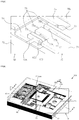
- FIG. 1 illustrates an exploded perspective view of an MEMS scanner according to an embodiment of the present invention.
- FIG. 2 illustrates a perspective view of the MEMS scanner of FIG. 1 .
- an MEMS scanner 100 includes a lower frame 10, a pair of upper frames 20, a pair of levers 40 and 50, a pair of fixed electrode portions 60 and 70, and a driving electrode portion 80.
- the lower frame 10 has cavities 11a and 11b formed downward from an upper surface of the lower frame, and a through-hole 17 between the cavities 11a and 11b.
- the pair of upper frames 20 are attached to the upper surface of the lower frame 10 near the cavities 11a and 11b, thereby forming an installation space 23 in the central portion between the upper frames.
- the pair of levers 40 and 50 are attached to both bottom surfaces of the cavities 11a and 11b with the through-hole 17 disposed therebetween, and are connected to the pair of upper frames 20, respectively.
- the driving electrode portion 80 has a plurality of driving electrodes 83a and 83b that are alternately disposed with respect to the fixed electrodes 63 and 73 of the pair of fixed electrode portions 60 and 70 and that are disposed in parallel on the upper surfaces of the respective upper frames 20 at both sides of the driving electrode portion.
- the MEMS scanner 100 has a structure in which the pair of upper frames 20, the pair of levers 40 and 50, the pair of fixed electrode portions 60 and 70, and the driving electrode portion 80 are installed on the top of the lower frame 10.
- the pair of upper frames 20, the pair of levers 40 and 50, the pair of fixed electrode portions 60 and 70, and the driving electrode portion 80 are provided as one original upper plate and then formed as the pair of upper frames 20, the pair of levers 40 and 50, the pair of fixed electrode portions 60 and 70, and the driving electrode portion 80 using the MEMS process.
- the pair of upper frames 20a and 20b include a first upper frame 20a and a second upper frame 20b disposed at both sides of the through-hole 17 of the lower frame 10, and one of the upper frames has a " ⁇ " shape and the other has a " ⁇ " shape to surround the through-hole 17. Both ends of which the first and second upper frames 20a and 20b meet are alternately formed.
- the pair of levers 40 and 50, the pair of fixed electrode portions 60 and 70, and the driving electrode portion 80 are installed inside the first and second upper frames 20a and 20b.
- the pair of levers 40 and 50 are fixed and connected inside the first and second upper frames 20a and 20b, respectively.
- the pair of levers 40 and 50 include a first lever 40 and a second lever 50.
- the first lever 40 is connected to the first upper frame 20a.
- the second lever 50 is connected to the second upper frame 20b.
- the fixed electrode portions 60 and 70 are rotatably connected to the first and second levers 40 and 50 inside the first and second levers 40 and 50, respectively.
- the pair of fixed electrode portions 60 and 70 include a first fixed electrode portion 60 and a second fixed electrode portion 70.
- the first fixed electrode portion 60 is rotatably connected to the first lever 40.
- the second fixed electrode portion 70 is rotatably connected to the second lever 50.
- the driving electrode portion 80 is installed between the first and second fixed electrode portions 60 and 70.
- the driving electrode portion 80 is spaced from the first and second fixed electrode portions 60 and 70 to be independently formed.
- the fixed electrodes 63 and 73 of the fixed electrode portions 60 and 70 are formed to be sloped by predetermined angles with respect to the driving electrodes 83a and 83b of the driving electrode portion 80 disposed in a horizontal direction using the cavities 11a and 11b formed on the upper surface of the lower frame 10.
- the slope of the fixed electrodes 63 and 73, that is, an initial angle is determined by the depth of the cavities 11a and 11b formed on the upper surface of the lower frame 10.
- the driving electrode portion 80 rotates toward the side to which the voltage is applied between the fixed electrode portions 60 and 70.
- the driving electrodes 83a and 83b of the driving electrode portion 80 rotate until the driving electrodes are in parallel on the fixed electrodes 63 and 73.
- the lower frame 10 provides a space on which the pair of upper frames 20, the pair of levers 40 and 50, the pair of fixed electrode portions 60 and 70, and the driving electrode portion 80 may be installed, and supports the pair of upper frames 20, the pair of levers 40 and 50, the pair of fixed electrode portions 60 and 70, and the driving electrode portion 80.
- the lower frame 10 has the cavities 11a and 11b formed by a predetermined depth from the upper surface of the lower frame, and the through-hole 17 is formed between the cavities 11a and 11b.
- the pair of fixed electrode portions 60 and 70 are attached to a periphery edge of the upper surface of the lower frame 10 outside the cavities 11a and 11b using a silicon oxide (SiO 2 ) film.
- a hinge installation portion 19 is formed at both sides of and near the through-hole 17.
- the fixed electrodes 63 and 73 and the driving electrodes 83a and 83b are disposed at both sides of the through-hole 17.
- the hinge installation portion 19 may be disposed at both sides adjacent to the sides in which the fixed electrodes 63 and 73 and the driving electrodes 83a and 83b are disposed.
- the cavities 11a and 11b include a first cavity 11a in which the first lever 40 and the first fixed electrode portion 60 are disposed, and a second cavity 11b in which the second lever 50 and the second fixed electrode portion 70 are disposed.
- the first cavity 11a is formed at one side of the through-hole 17 and the second cavity 11b is formed at the opposite side thereof.
- the first cavity 11a includes a first lever fixed surface 13a in which the first lever 40 is installed, and a first fixing installation surface 15a in which the first fixed electrode portion 60 is installed.
- the second cavity 11b includes a second lever fixed surface 13b in which the second lever 50 is installed, and a second fixing installation surface 15b in which the second fixed electrode portion 70 is installed.
- the cavities 11a and 11b include a first hinge installation piece space portion 16 and a second hinge installation piece space portion 18 formed at both sides of the hinge installation portion 19. Hinge installation pieces 65 and 75 of the first and second fixed electrode portions 60 and 70 are floated and positioned above the first and second hinge installation piece space portions 16 and 18.
- the driving electrode portion 80 is disposed above the through-hole 17 disposed in the central portion between the cavities 11a and 11b.
- the through-hole 17 may prevent a mechanical interference between the driving electrode portion 80 and the lower frame 10 from occurring while the driving electrode portion 80 rotates.
- the through-hole 17 allows a fluid, for example, an air, present within the cavities 11a and 11b to be discharged through the through-hole 17 while the driving electrode portion 80 rotates, thereby reducing the reduction in rotational angle caused by the fluidal resistance during rotation of the driving electrode portion 80.
- the through-hole 17 may be used as a discharge port allowing an adhesive to be discharged through the through-hole 17 without adhering to the driving electrode portion 80 when the first and second levers 40 and 50 are bonded to the first and second lever fixed surfaces 13a and 13b of the lower frame 10 in a process of manufacturing the MEMS scanner 100, respectively.
- the lower frame 10 may be formed of silicon, glass, or ceramic.
- a wafer formed of silicon may be used to form the pair of upper frames 20, the pair of levers 40 and 50, the pair of fixed electrode portions 60 and 70, and the driving electrode portion 80, which are disposed on the lower frame 10.
- the pair of upper frames 20a and 20b include the first upper frame 20a and the second upper frame 20b as described above.
- the first upper frame 20a surrounds the outside of the first lever 40, and is attached to the upper surface of the lower frame 10.
- the second upper frame 20b surrounds the outside of the second lever 50 and is attached to the upper surface of the lower frame 10, and the second upper frame 20b along with the first upper frame 20a forms the installation space 23 at the central portion.
- the pair of levers 40 and 50, the pair of fixed electrode portions 60 and 70, and the driving electrode portion 80 are disposed in the installation space 23.
- Both ends of the first and second upper frames 20a and 20b are alternately formed, and first and second hinge connection pieces 21a and 21b are formed in the alternating portions.
- the pair of second hinge connection pieces 21b may be formed inside the pair of first hinge connection pieces 21a formed at both sides thereof.
- the first and second hinge connection pieces 21a and 21b are attached to the hinge installation portion 19 formed in the lower frame 10.
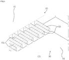
- FIG. 3 illustrates an enlarged view of the "A" portion of FIG. 2 .
- the first and second levers 40 and 50 are installed inside the first and second upper frames 20a and 20b, respectively.
- the first and second levers 40 and 50 have a pair of connection plates 42 and 52 and lever plates 48 and 58, respectively.
- the pair of connection plates 42 and 52 are connected to the upper frames 20a and 20b using first lever hinges 43 and 53, respectively.
- Both ends of one side of the lever plates 48 and 58 are connected to the pair of respective connection plates 42 and 52 using respective second lever hinges 45 and 55, and are fixed to the bottom surfaces of the respective cavities 11a and 11b, and both ends of the other side thereof are connected to the respective fixed electrode portions 60 and 70 using respective third lever hinges 47 and 57.
- the third lever hinges 47 and 57 of the first and second levers 40 and 50 are positioned at sides closer to the through-hole 17 with the first lever hinges 43 and 53 as a center, and the second lever hinges 45 and 55 are positioned at sides opposite to the sides at which the third lever hinges 47 and 57 are positioned.
- a plurality of adhesive injection holes 41 and 51 are formed to penetrate the respective lever plates 48 and 58, and the lever plates 48 and 58 are attached to the respective bottom surfaces of the cavities 11a and 11b, that is, the respective first and second lever fixed surfaces 13a and 13b using the adhesive injected through the plurality of adhesive injection holes 41 and 51.
- the lever plates 48 and 58 are press-attached to the first and second lever fixed surfaces 13a and 13b of the cavities 11a and 11b, respectively.
- an adhesive layer 33 is formed between the first and second lever fixed surfaces 13a and 13b of the cavities 11a and 11b and the lever plates 48 and 58.
- a silicon-based or epoxy-based adhesive may be employed as the adhesive 31.
- FIG. 6 illustrates a perspective view in which the levers 40 and 50 of FIG. 2 are attached to the bottom surfaces of the cavities of the lower frame 10.
- FIG. 7 illustrates an enlarged view of the "D" portion of FIG. 6 .
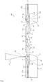
- FIG. 8 illustrates a cross-sectional view taken along the 8-8 line of FIG. 6 .
- first lever 40 and the second lever 50 are formed with the structure at both sides of the first and second upper frames 20a and 20b, respectively.
- the first lever 40 has the first connection plate 42, the first lever plate 48 in which the first adhesive injection hole 41 is formed, the 1-1 lever hinge 43, the 2-1 lever hinge 45, and the 3-1 lever hinge 47.
- the second lever 50 has the second connection plate 52, the second lever plate 58 in which the second adhesive injection hole 51 is formed, the 1-2 lever hinge 53, the 2-2 lever hinge 55, and the 3-2 lever hinge 57.
- FIG. 4 illustrates an enlarged view of the "B" portion of FIG. 2 .
- the first and second fixed electrode portions 60 and 70 include fixed electrode frames 61 and 71, the plurality of fixed electrodes 63 and 73, and the hinge installation pieces 65 and 75, respectively.
- the fixed electrode frames 61 and 71 are connected to the levers 40 and 50 using the third lever hinges 47 and 57.
- the plurality of fixed electrodes 63 and 73 are arranged at one side of the fixed electrode frames 61 and 71 toward the through-hole 17.
- the hinge installation pieces 65 and 75 are arranged toward both sides of the fixed electrode frames 61 and 71 with the plurality of fixed electrodes 63 and 73 as centers, and are connected to the hinge connection pieces 21a and 21b of the upper frames 20a and 20b using fixed hinges 67 and 77, respectively.
- the hinge installation piece space portions 16 and 18 are formed below the hinge installation pieces 65 and 75 to allow the hinge installation pieces 65 and 75 to rotate around the fixed hinges 67 and 77 with respect to the upper frames 20a and 20b, respectively.
- the first and second fixed electrode portions 60 and 70 are formed with the same structure at both sides of the first and second levers 40 and 50, respectively.
- the first fixed electrode portion 60 includes the first fixed electrode frame 61, the plurality of first fixed electrodes 63, the first hinge installation piece 65, and the first fixed hinge 67.
- the second fixed electrode portion 70 includes the second fixed electrode frame 71, the plurality of second fixed electrodes 73, the second hinge installation piece 75, and the second fixed hinge 77.
- the second hinge installation piece 75 of the second fixed electrode portion 70 is disposed inside the first hinge installation piece 65 of the first fixed electrode portion 60.
- the first hinge installation piece 65 is installed to be floated above the first hinge installation piece space portion 16 so as to allow the first hinge installation piece 65 to rotate around the first fixed hinge 67 with respect to the upper frame 20.
- the second hinge installation piece 75 includes a 2-1 hinge installation piece 75a, and 2-2 and 2-3 hinge installation pieces 75b and 75c disposed at both sides of the 2-1 hinge installation piece 75a so as to allow the second hinge installation piece to be stably installed in the hinge installation portion 19.
- the 2-1 hinge installation piece 75a as a center
- the 2-2 hinge installation piece 75b is disposed to the side in which the first fixed hinge 67 is installed
- the 2-3 hinge installation piece 75c is disposed to the opposite side.
- the 2-1 hinge installation piece 75a and the 2-2 hinge installation piece 75b are connected using a 2-2 fixed hinge 77b.
- the 2-1 hinge installation piece 75a and the 2-3 hinge installation piece 75c are connected using a 2-1 fixed hinge 77a.
- the second fixed hinge 77 includes the 2-1 fixed hinge 77a and the 2-2 fixed hinge 77b.
- the 2-1 hinge installation piece 75a is installed to be floated above the second hinge installation piece space portion 18 so as to allow the 2-1 hinge installation piece 75a to rotate around the second fixed hinge 77 with respect to the upper frame 20.
- the second hinge installation piece 75 is illustrated to be inside the first hinge installation piece 65 in the present embodiment, the present invention is not limited thereto.
- the first hinge installation piece 65 and the second hinge installation piece 75 may be alternately formed. That is, the second hinge installation piece 75 may be formed inside the first hinge installation piece 65 at one side and the first hinge installation piece 65 may be formed inside the second hinge installation piece 75 at the other side.
- Each of the first and second fixed electrodes 63 and 73 may be arranged in a row so that the first fixed electrodes face the second fixed electrodes, and a space in which the driving electrode portion 80 is installed is formed between the first and second fixed electrodes 63 and 73.
- the first and second fixed electrodes 63 and 73 may be interdigitated to have respective rectangular plate shapes.
- the first and second fixed electrodes 63 and 73 are sloped to a constant angle, that is, an initial angle with respect to the horizontal surface as shown in FIGS. 6 and 7 when the lever plates 48 and 58 of the levers 40 and 50 are attached to the first and second lever fixed surfaces 13a and 13b of the cavities 11a and 11b, respectively.
- the first and second fixed hinges 67 and 77 are positioned on the same axis so as to allow the first and second fixed electrodes 63 and 73 to be sloped to the same initial angle.
- the first and second fixed electrodes 63 and 73 are arranged at an equal interval at both sides with the first and second fixed hinges 67 and 77 as an axis, respectively.
- first and second levers 40 and 50 are attached to the first and second lever fixed surfaces 13a and 13b of the cavities 11a and 11b of the lower frame 10 and the first and second fixed hinges 67 and 77 of the first and second fixed electrode portions 60 and 70 are positioned on the upper surface of the lower frame 10, the first and second fixed electrode portions 60 and 70 rotate around the respective first and second fixed hinges 67 and 77 to allow the first and second fixed electrodes 63 and 73 to form the initial angle with respect to the horizontal surface.
- FIG. 5 illustrates an enlarged view of the "C" portion of FIG. 2 .
- the driving electrode portion 80 includes a driving electrode frame 81, the plurality of driving electrodes 83a and 83b, a pair of spring installation pieces 85a and 85b, and the pair of rotational springs 87a and 87b.
- the driving electrode frame 81 is disposed in a space between the first and second fixed electrodes 63 and 73.
- the plurality of driving electrodes 83a and 83b are formed at sides in which the driving electrode frame 81 faces the first and second fixed electrodes 63 and 73, and are disposed alternately with respect to the first and second fixed electrodes 63 and 73, respectively.
- the pair of spring installation pieces 85a and 85b are fixed to the upper surface of the lower frame 10 at both sides adjacent to the sides in which the plurality of driving electrodes 83a and 83b are formed.
- the pair of rotational springs 87a and 87b connect the pair of spring installation pieces 85a and 85b with the driving electrode frame 81.
- the plurality of driving electrodes 83a and 83b may be interdigitated to have a rectangular shape corresponding to the fixed electrodes 63 and 73.
- the fixed electrodes 63 and 73 and the respective driving electrodes 83a and 83b are alternately disposed.
- the plurality of driving electrodes 83a and 83b include the first driving electrodes 83a alternately installed with respect to the first fixed electrodes 63, and the second driving electrodes 83b alternately installed with respect to the second fixed electrodes 73.
- the driving electrodes 83a and 83b supported by the spring installation pieces 85a and 85b are horizontally installed, and the fixed electrodes 63 and 73 are disposed to be sloped to a constant angle with respect to the horizontally installed driving electrodes 83a and 83b.
- the spring installation pieces 85a and 85b are attached to the hinge installation portion 19, and are positioned inside the 2-3 hinge installation piece 75c.
- the rotational springs 87a and 87b are positioned on the same axis as the first and second fixed hinges 67 and 77.
- the reason why the rotational springs 87a and 87b are positioned on the same axis as the first and second fixed hinges 67 and 77 is as follows.
- the driving electrode portion 80 statically rotates, the driving electrodes 83a and 83b may rotate until the driving electrodes are in parallel on the fixed electrodes 63 and 73. This moment corresponds to the angle by which the driving electrodes 83a and 83b can rotate geometrically as much as possible.
- the driving electrode portion 80 according to the present embodiment along with the fixed electrode portions 60 and 70 is supported by the lower frame 10 but is physically separated from the fixed electrode portions, the driving electrode portion and the fixed electrode portions structurally do not have an influence on each other.
- the driving electrode portion 80 can thus have no physical influence from the fixed electrode portions 60 and 70 while rotating in accordance with the potential difference generated between the driving electrode portion 80 and the fixed electrode portions 60 and 70.
- the rotational springs 87a and 87b of the driving electrode portion 80 are in a state in which an elasticity generated from the torsion is not applied when there is no voltage applied, fatigue failures due to long-term use can be avoided.
- the MEMS scanner 100 according to the present embodiment may be manufactured as follows.
- the MEMS scanner 100 according to the present embodiment may be manufactured in the order of manufacturing the lower frame 10, bonding an original upper plate to the lower frame, and having the original upper plate being subjected to Si DRIE (deep reactive ion etching) to form the pair of upper frames 20, the pair of levers 40 and 50, the pair of fixed electrode portions 60 and 70, and the driving electrode portion 80.
- Si DRIE deep reactive ion etching
- the cavities 11a and 11b and the through-hole 17 are formed in the lower frame 10 using the MEMS process.
- a silicon oxide film 12 is grown on the lower frame 10 and the original upper plate, and the original upper plate is bonded to the lower frame 10.
- the pair of upper frames 20, the pair of levers 40 and 50, the pair of fixed electrode portions 60 and 70, and the driving electrode portion 80 are manufactured in the bonded original upper plate using the Si DRIE process.
- the spring installation pieces 85a and 85b of the driving electrode portion 80 and the hinge installation pieces 65 and 75 of the fixed electrode portions 60 and 70 are positioned on the hinge installation portion 19 of the lower frame 10.
- the spring installation pieces 85a and 85b and the hinge installation pieces 65 and 75 are structurally separated from each other using the Si DRIE process.
- the adhesive 31 is injected through the adhesive injection holes 41 and 51 of the levers 40 and 50, and only the levers 40 and 50 are pressed and bonded to the first and second lever fixed surfaces 13a and 13b of the cavities 11a and 11b of the lower frame 10, thereby manufacturing the MEMS scanner 100 according to the present embodiment.
- FIGS. 9 to 12 are views illustrating driving of the MEMS scanner 100 according to an embodiment of the present invention.
- the fixed electrodes are inclined to the initial angle ⁇ with respect to the driving electrodes 83a and 83b in the MEMS scanner 100 according to the present embodiment.
- the second fixed electrode 73 is inclined to the initial angle ⁇ with respect to the second driving electrode 83b.
- the first fixed electrode 63 may also be inclined to the same initial angle ⁇ with respect to the first driving electrode 83a.
- the driving electrode portion 80 rotates in a counterclockwise direction using the torsion elasticity force accumulated on the rotational spring to restore to the original horizontal position.
- the driving electrode portion 80 rotates in a counterclockwise direction toward the first fixed electrode portion 60 to which the voltage is applied.
- the driving electrode portion 80 rotates to the maximum, the first driving electrode 83a is disposed in parallel on the first fixed electrode.
- the driving electrode portion 80 rotates in a clockwise direction using the torsion elasticity force accumulated on the rotational spring to restore to the original horizontal position.
- the MEMS scanner 100 is a micro-actuator actuated by an electrostatic force, and may be implemented as a mirror scanner, lens scanner, or the like.
- the MEMS scanner 100 is implemented as the mirror scanner.
- a metallic film may be deposited on the driving electrode portion 80 including the mirror and the fixed electrode portions 60 and 70. Gold or aluminum may be used to form the metallic film.
- the MEMS scanner 100 is implemented as the lens scanner.
- a metallic film may be deposited on the driving electrode portion 80 and the fixed electrode portions 60 and 70 except the lens. Gold or aluminum may be used to form the metallic film.
Landscapes
- Physics & Mathematics (AREA)
- Engineering & Computer Science (AREA)
- General Physics & Mathematics (AREA)
- Optics & Photonics (AREA)
- Microelectronics & Electronic Packaging (AREA)
- Computer Hardware Design (AREA)
- Multimedia (AREA)
- Signal Processing (AREA)
- Manufacturing & Machinery (AREA)
- Chemical & Material Sciences (AREA)
- Analytical Chemistry (AREA)
- Mechanical Light Control Or Optical Switches (AREA)
Description
- The present invention relates to a micro electro mechanical systems (MEMS) scanner, and more particularly, to an MEMS scanner for implementing stable driving while increasing a driving angle between a fixed electrode and a driving electrode using an MEMS process.
- Recently, research on micro electro mechanical systems (MEMS) devices manufactured by semiconductor process techniques has been actively in progress in various technical fields such as displays, printing devices, precision measuring, precision processing, or the like. For example, an optical scanner having a micro structure is drawing attention in a display field in which light incident from a light source is radiated on a predetermined screen area to implement a video or a scanning field in which light is scanned on a predetermined screen area and reflected light is received to read out image information.
- Such an optical scanner refers to one in which a reflective mirror for reflecting light, a support axis for supporting the reflective mirror, and driving means for moving the reflective mirror are implemented as a single chip.
- A comb-shaped driver has driving electrodes that are disposed in parallel on the plane of a moving structure or a stage that is a moving object, and fixed electrodes corresponding to the driving electrodes have a structure in which the fixed electrodes are alternately disposed with respect to the driving electrodes while being fixed and are disposed in parallel on the plane surface of the stage along with the driving electrodes.
- In order to allow the electrostatic type driver to have a rotational movement in an electrostatic driving condition, a height difference or a slope is required between the driving electrode and the fixed electrode. Since an additional process for causing one of the driving electrode and the fixed electrode to have a different height or an additional process for causing the height to be inclined after making both heights same as each other is required for the comb-shaped driver, it becomes complicated to manufacture the optical scanner.
- Methods of forming an initial angle for the driving electrode are as follows.
- First, a method may be employed which deposits a polymer between an upper end of a driving electrode and an upper end of a driving portion to connect the driving electrode with the driving portion, and heat-deforms the polymer to shrink the polymer, thereby inclining the driving electrode. There are limits to this method in terms of high speed driving of the optical scanner, complicated manufacturing processes, and a manufacturing reproducibility for forming a constant initial angle of the driving electrode.
- Another method is to have a rotational spring subjected to plastic deformation using Joule heating while the spring is intentionally inclined to form an initial angle. There is a limit to this method in terms of the driving angle because the optical scanner can only be driven in uni-direction at the time of electrostatically driving the optical scanner.
- Yet another method is to form an initial angle using an assembly. According to this method, an additional separate structure needs to be coupled to an optical scanner in order to form the initial angle for the driving electrode, which thus causes the manufacturing process to be complicated and the manufacturing cost to be increased. In addition, a volume of the optical scanner is inevitably increased due to the added structure. Moreover, since a spring of the driving portion and a hinge of the fixed electrode are structurally connected to each other, the spring of the driving portion and the driving electrode also simultaneously rotate when the fixed electrode is inclined, so that the initial angle is not formed. Accordingly, in order to prevent the driving electrode from being rotated, the spring of the driving portion needs to be intentionally twisted, which causes the spring of the driving portion to have a residual stress even when the optical scanner is not driven. This causes unstable driving such as fatigue failures in the long term and a poor impact resistance to occur in terms of driving the optical scanner.
-
US 2009/244668 A1 relates to background art. - The present invention is thus directed to providing an MEMS scanner for implementing stable driving while increasing a driving angle between a fixed electrode and a driving electrode using an MEMS process.
- The present invention is also directed to providing a method capable of reducing a manufacturing cost while having an MEMS scanner small-sized by means of manufacturing process simplification.
- An MEMS scanner for implementing stable driving while increasing a driving angle between a fixed electrode and a driving electrode using an MEMS process is disclosed in claim 1. Advantageous developments are the subject-matter of the dependent claims.
- One aspect of the present invention provides an MEMS scanner including a lower frame, a pair of upper frames, a pair of levers, a pair of fixed electrode portions, and a driving electrode portion. The lower frame has cavities downward from an upper surface of the lower frame, and a through-hole is formed between the cavities. The pair of upper frames are attached to the upper surface of the lower frame near the cavities to form an installation space in a central portion between the upper frames. The pair of levers are disposed inside the respective upper frames, are attached to both sides of a bottom surface of the cavities around the through-hole, and are connected to the respective upper frames. The pair of fixed electrode portions of which one side is connected to the respective levers and the other side is connected to the respective upper frames have a plurality of fixed electrodes that can be sloped toward an upper surface of the upper frames with respect to the bottom surface of the cavities, and the plurality of fixed electrodes are formed toward the through-hole. The driving electrode portion has a plurality of driving electrodes formed at both sides thereof, the plurality of driving electrodes are alternately disposed with respect to the fixed electrodes of the pair of fixed electrode portions and are disposed in parallel on the upper surfaces of the respective upper frames, and sides opposite to the both sides in which the plurality of driving electrodes are disposed are attached to the upper surface of the lower frame using respective rotational springs. In this case, when a voltage is applied between the driving electrode portion and one of the pair of fixed electrode portions to generate a potential difference, the driving electrode portion rotates toward the fixed electrode portion to which the voltage is applied.
- In the MEMS scanner according to the present invention, the pair of upper frames may include a first upper frame and a second upper frame. The first upper frame may surround an outer surface of a first lever of the pair of levers and may be attached to the upper surface of the lower frame. The second upper frame may surround an outer surface of a second lever of the pair of levers, may be attached to the upper surface of the lower frame, and may form an installation space in a central portion between the first and second upper frames. In this case, the pair of levers, the pair of fixed electrode portion, and the driving electrode portion may be positioned in the installation space.
- In the MEMS scanner according to the present invention, the pair of fixed electrode portions may be disposed to surround an outer surface of the driving electrode portion with the driving electrode portion as a center, and the levers may be disposed rear of the pair of fixed electrode portions, respectively.
- In the MEMS scanner according to the present invention, each of the pair of levers may include a pair of connection plates and lever plates. The pair of connection plates may be connected to the respective upper frames at both sides of the connection plates using a first lever hinge. Both ends of one side of the lever plates may be connected to the respective connection plates using a second lever hinge, the lever plates may be fixed to the bottom surface of the cavities, and both ends of the other side of the lever plates may be connected to the respective fixed electrode portions using a third lever hinge.
- In the MEMS scanner according to the present invention, the third lever hinge of the pair of levers may be positioned at a side closer to the through-hole with the first lever hinge as a center, and the second lever hinges may be positioned at a side opposite to the sides at which the third lever hinge is positioned.
- In the MEMS scanner according to the present invention, a plurality of adhesive injection holes may be formed to penetrate each of the lever plates. The lever plates may be attached to the bottom surface of the respective cavities using the adhesive injected through the plurality of adhesive injection holes.
- In the MEMS scanner according to the present invention, each of the pair of fixed electrode portions may include a fixed electrode frame, a plurality of fixed electrodes, and a hinge installation piece. The fixed electrode frame may be connected to the lever using the third lever hinge. The plurality of fixed electrodes may be arranged at one side of the fixed electrode frame toward the through-hole. The hinge installation piece may extend to both sides of the fixed electrode frame with the plurality of fixed electrodes as a center, and may be connected to the fixed electrode frame using fixed hinges.
- In the MEMS scanner according to the present invention, the hinge installation pieces may be disposed on the cavities.
- In the MEMS scanner according to the present invention, the fixed electrodes of the pair of fixed electrode portions may be spaced from each other to form a space in which the driving electrode portion is installed.
- In the MEMS scanner according to the present invention, the driving electrode portion may include a driving electrode frame, a plurality of driving electrodes, a pair of spring installation pieces, and a pair of rotational springs. The driving electrode frame may be disposed in a space between the fixed electrodes of the pair of fixed electrode portions. The plurality of driving electrodes may be formed at sides of the driving electrode frame in which the fixed electrodes of the pair of fixed electrode portions face, and may be disposed alternately with respect to the fixed electrodes of the pair of fixed electrode portions. The pair of spring installation pieces may be formed at both sides adjacent to sides in which the plurality of driving electrodes are formed, and may be fixed to the upper surface of the lower frame. The pair of rotational springs may connect the spring installation pieces with the driving electrode frame.
- In the MEMS scanner according to the present invention, the fixed hinges and the rotational springs may be disposed on the same axis.
- In the MEMS scanner according to the present invention, when a voltage is applied between the driving electrode portion and one of the pair of fixed electrode portions to generate a potential difference, the driving electrode portion may rotate toward the fixed electrode portion to which the voltage is applied, and the driving electrodes may rotate until the driving electrode portion is in parallel on the fixed electrode portions.
- In the MEMS scanner according to the present invention, the fixed electrodes and the driving electrodes may be interdigitated.
- In the MEMS scanner according to the present invention, a mirror may be formed in the driving electrode frame of the driving electrode portion, or a portion of the driving electrode frame may be penetrated and a lens may be coupled to the penetrated portion.
- In the MEMS scanner according to the present invention, when a mirror is formed in the driving electrode frame of the driving electrode portion, a metallic film may be deposited on the driving electrode portion including the mirror and the fixed electrode portions.
- In the MEMS scanner according to the present invention, when a lens is coupled to the driving electrode frame of the driving electrode portion, a metallic film may be deposited on the driving electrode portion and the fixed electrode portions except the lens.
- In the MEMS scanner according to the present invention, the metallic film may be formed of gold or aluminum.
- An MEMS scanner according to the present invention can implement stable driving while increasing a driving angle between a fixed electrode and a driving electrode using a step of cavities formed in a lower frame manufactured through an MEMS process.
- In addition, since a driving electrode portion along with fixed electrode portions is supported by the lower frame but is physically separated from the fixed electrode portions, the driving electrode portion and the fixed electrode portions structurally do not have an influence on each other. It is thus possible for the driving electrode portion to rotate in accordance with a potential difference generated between the driving electrode portion and the fixed electrode portions while not being physically influenced by the fixed electrode portions. In addition, since rotational springs of the driving electrode portion are positioned with no elasticity caused by torsion when a voltage is not applied, it is possible to suppress fatigue failures caused by a long term use.
- In addition, the MEMS scanner according to the present invention is manufactured by the MEMS process in the order of manufacturing a lower frame and then stacking an original upper plate on the lower frame. A pair of upper frames, a pair of levers, a pair of fixed electrode portions, and a driving electrode portion are then manufactured on the original upper plate using a silicon deep reactive ion etch (Si DRIE) process and only the levers are attached to cavities of the lower frame, thereby allowing a process of additionally manufacturing individual structures for inclining the fixed electrode portions as in the related art to be omitted. As a result, the MEMS scanner can be small-sized and the manufacturing cost can be reduced using the manufacturing process simplification of the MEMS scanner.
-
-
FIG. 1 illustrates an exploded perspective view of an MEMS scanner according to an embodiment of the present invention. -
FIG. 2 illustrates a perspective of the MEMS scanner ofFIG. 1 . -
FIG. 3 illustrates an enlarged view of the "A" portion ofFIG. 2 . -
FIG. 4 illustrates an enlarged view of the "B" portion ofFIG. 2 . -
FIG. 5 illustrates an enlarged view of the "C" portion ofFIG. 2 . -
FIG. 6 illustrates a perspective view of which a lever ofFIG. 2 is attached to a bottom of a cavity of a lower fixing portion. -
FIG. 7 illustrates an enlarged view of the "D" portion ofFIG. 6 . -
FIG. 8 illustrates a cross-sectional view taken along the 8-8 line ofFIG. 6 . -
FIGS. 9 to 12 are views illustrating driving of an MEMS scanner according to an embodiment of the present invention. - Note that only portions necessary to understand embodiments of the present invention will be described hereinafter, and the other portions will be omitted in a range that does not obscure the gist of the present invention.
- Terms or words used herein and the following claims should not be construed as limited to conventional or dictionary definition but as meanings and concepts meeting the technical spirit of the present invention based on the principle that the inventor could appropriately define concepts of the terms to describe the best mode of the invention. Accordingly, configurations illustrated in embodiments and drawings used herein are merely preferred embodiments of the present invention and do not represent all technical spirits of the present invention, and it will be understood that various equivalents and modifications may be made to replace the embodiments at the time of filing the present application.
- Hereinafter, embodiments of the present invention will be described in detail with reference to accompanying drawings.
-
FIG. 1 illustrates an exploded perspective view of an MEMS scanner according to an embodiment of the present invention.FIG. 2 illustrates a perspective view of the MEMS scanner ofFIG. 1 . - Referring to
FIGS. 1 and2 , anMEMS scanner 100 according to the present embodiment includes alower frame 10, a pair ofupper frames 20, a pair oflevers electrode portions electrode portion 80. Thelower frame 10 hascavities hole 17 between thecavities upper frames 20 are attached to the upper surface of thelower frame 10 near thecavities installation space 23 in the central portion between the upper frames. The pair oflevers cavities hole 17 disposed therebetween, and are connected to the pair ofupper frames 20, respectively. One end of fixedelectrode portions respective levers upper frames 20, the pair of fixed electrode portions have a plurality of fixedelectrodes upper frames 20 with respect to the bottom surfaces of thecavities electrodes hole 17. The drivingelectrode portion 80 has a plurality of drivingelectrodes electrodes electrode portions upper frames 20 at both sides of the driving electrode portion. Sides opposite to sides in which the plurality of drivingelectrodes upper frames 20 usingrotational springs electrode portion 80 and one of the fixedelectrode portions electrode portion 80 rotates toward the side to which the voltage is applied between the fixedelectrode portions - The
MEMS scanner 100 according to the present embodiment as described above has a structure in which the pair ofupper frames 20, the pair oflevers electrode portions electrode portion 80 are installed on the top of thelower frame 10. The pair ofupper frames 20, the pair oflevers electrode portions electrode portion 80 are provided as one original upper plate and then formed as the pair ofupper frames 20, the pair oflevers electrode portions electrode portion 80 using the MEMS process. - The pair of
upper frames upper frame 20a and a secondupper frame 20b disposed at both sides of the through-hole 17 of thelower frame 10, and one of the upper frames has a "⊂" shape and the other has a "⊃" shape to surround the through-hole 17. Both ends of which the first and secondupper frames - The pair of
levers electrode portions electrode portion 80 are installed inside the first and secondupper frames levers upper frames levers first lever 40 and asecond lever 50. Thefirst lever 40 is connected to the firstupper frame 20a. Thesecond lever 50 is connected to the secondupper frame 20b. - The fixed
electrode portions second levers second levers electrode portions fixed electrode portion 60 and a secondfixed electrode portion 70. The firstfixed electrode portion 60 is rotatably connected to thefirst lever 40. The secondfixed electrode portion 70 is rotatably connected to thesecond lever 50. - The driving
electrode portion 80 is installed between the first and secondfixed electrode portions electrode portion 80 is spaced from the first and secondfixed electrode portions - The fixed
electrodes electrode portions electrodes electrode portion 80 disposed in a horizontal direction using thecavities lower frame 10. The slope of the fixedelectrodes cavities lower frame 10. - In the
MEMS scanner 100 according to the present embodiment as described above, when a voltage is applied between the drivingelectrode portion 80 and one of the pair of fixedelectrode portions electrode portion 80 rotates toward the side to which the voltage is applied between the fixedelectrode portions electrodes electrode portion 80 rotate until the driving electrodes are in parallel on the fixedelectrodes - Each component of the
MEMS scanner 100 according to the present embodiment will be described in detail. - The
lower frame 10 provides a space on which the pair ofupper frames 20, the pair oflevers electrode portions electrode portion 80 may be installed, and supports the pair ofupper frames 20, the pair oflevers electrode portions electrode portion 80. Thelower frame 10 has thecavities hole 17 is formed between thecavities - The pair of fixed
electrode portions lower frame 10 outside thecavities hinge installation portion 19 is formed at both sides of and near the through-hole 17. In this case, the fixedelectrodes electrodes hole 17. Thehinge installation portion 19 may be disposed at both sides adjacent to the sides in which the fixedelectrodes electrodes - The
cavities first cavity 11a in which thefirst lever 40 and the firstfixed electrode portion 60 are disposed, and asecond cavity 11b in which thesecond lever 50 and the secondfixed electrode portion 70 are disposed. Thefirst cavity 11a is formed at one side of the through-hole 17 and thesecond cavity 11b is formed at the opposite side thereof. - The
first cavity 11a includes a first lever fixedsurface 13a in which thefirst lever 40 is installed, and a firstfixing installation surface 15a in which the firstfixed electrode portion 60 is installed. Thesecond cavity 11b includes a second lever fixedsurface 13b in which thesecond lever 50 is installed, and a secondfixing installation surface 15b in which the secondfixed electrode portion 70 is installed. - The
cavities piece space portion 16 and a second hinge installationpiece space portion 18 formed at both sides of thehinge installation portion 19.Hinge installation pieces fixed electrode portions piece space portions - The driving
electrode portion 80 is disposed above the through-hole 17 disposed in the central portion between thecavities hole 17 may prevent a mechanical interference between the drivingelectrode portion 80 and thelower frame 10 from occurring while the drivingelectrode portion 80 rotates. In addition, the through-hole 17 allows a fluid, for example, an air, present within thecavities hole 17 while the drivingelectrode portion 80 rotates, thereby reducing the reduction in rotational angle caused by the fluidal resistance during rotation of the drivingelectrode portion 80. In addition, the through-hole 17 may be used as a discharge port allowing an adhesive to be discharged through the through-hole 17 without adhering to the drivingelectrode portion 80 when the first andsecond levers surfaces lower frame 10 in a process of manufacturing theMEMS scanner 100, respectively. - The
lower frame 10 may be formed of silicon, glass, or ceramic. A wafer formed of silicon may be used to form the pair ofupper frames 20, the pair oflevers electrode portions electrode portion 80, which are disposed on thelower frame 10. - The pair of
upper frames upper frame 20a and the secondupper frame 20b as described above. The firstupper frame 20a surrounds the outside of thefirst lever 40, and is attached to the upper surface of thelower frame 10. The secondupper frame 20b surrounds the outside of thesecond lever 50 and is attached to the upper surface of thelower frame 10, and the secondupper frame 20b along with the firstupper frame 20a forms theinstallation space 23 at the central portion. The pair oflevers electrode portions electrode portion 80 are disposed in theinstallation space 23. - Both ends of the first and second
upper frames hinge connection pieces hinge connection pieces 21b may be formed inside the pair of firsthinge connection pieces 21a formed at both sides thereof. The first and secondhinge connection pieces hinge installation portion 19 formed in thelower frame 10. - The first and
second levers FIGS. 1 to 3 . In this case,FIG. 3 illustrates an enlarged view of the "A" portion ofFIG. 2 . - The first and
second levers upper frames second levers connection plates lever plates connection plates upper frames lever plates respective connection plates respective cavities electrode portions - In addition, the third lever hinges 47 and 57 of the first and
second levers hole 17 with the first lever hinges 43 and 53 as a center, and the second lever hinges 45 and 55 are positioned at sides opposite to the sides at which the third lever hinges 47 and 57 are positioned. - A plurality of adhesive injection holes 41 and 51 are formed to penetrate the
respective lever plates lever plates cavities surfaces FIGS. 6 to 8 , after an adhesive 31 is injected into the adhesive injection holes 41 and 51 by anadhesive supply member 30, thelever plates surfaces cavities adhesive layer 33 is formed between the first and second lever fixedsurfaces cavities lever plates - Since the
lever plates surfaces cavities electrodes electrode portions lever plates lever plates connection plates FIG. 6 illustrates a perspective view in which thelevers FIG. 2 are attached to the bottom surfaces of the cavities of thelower frame 10.FIG. 7 illustrates an enlarged view of the "D" portion ofFIG. 6 .FIG. 8 illustrates a cross-sectional view taken along the 8-8 line ofFIG. 6 . - In this case, the
first lever 40 and thesecond lever 50 are formed with the structure at both sides of the first and secondupper frames first lever 40 has thefirst connection plate 42, thefirst lever plate 48 in which the firstadhesive injection hole 41 is formed, the 1-1lever hinge 43, the 2-1lever hinge 45, and the 3-1lever hinge 47. Thesecond lever 50 has thesecond connection plate 52, thesecond lever plate 58 in which the secondadhesive injection hole 51 is formed, the 1-2lever hinge 53, the 2-2lever hinge 55, and the 3-2lever hinge 57. - The first and second
fixed electrode portions FIGS. 1 ,2 , and4 . In this case,FIG. 4 illustrates an enlarged view of the "B" portion ofFIG. 2 . - The first and second
fixed electrode portions electrodes hinge installation pieces levers electrodes hole 17. Thehinge installation pieces electrodes hinge connection pieces upper frames piece space portions hinge installation pieces hinge installation pieces upper frames - The first and second
fixed electrode portions second levers fixed electrode portion 60 includes the firstfixed electrode frame 61, the plurality of firstfixed electrodes 63, the firsthinge installation piece 65, and the firstfixed hinge 67. The secondfixed electrode portion 70 includes the secondfixed electrode frame 71, the plurality of secondfixed electrodes 73, the secondhinge installation piece 75, and the secondfixed hinge 77. - The second
hinge installation piece 75 of the secondfixed electrode portion 70 is disposed inside the firsthinge installation piece 65 of the firstfixed electrode portion 60. The firsthinge installation piece 65 is installed to be floated above the first hinge installationpiece space portion 16 so as to allow the firsthinge installation piece 65 to rotate around the firstfixed hinge 67 with respect to theupper frame 20. - The second
hinge installation piece 75 includes a 2-1hinge installation piece 75a, and 2-2 and 2-3hinge installation pieces hinge installation piece 75a so as to allow the second hinge installation piece to be stably installed in thehinge installation portion 19. With the 2-1hinge installation piece 75a as a center, the 2-2hinge installation piece 75b is disposed to the side in which the firstfixed hinge 67 is installed, and the 2-3hinge installation piece 75c is disposed to the opposite side. The 2-1hinge installation piece 75a and the 2-2hinge installation piece 75b are connected using a 2-2fixed hinge 77b. The 2-1hinge installation piece 75a and the 2-3hinge installation piece 75c are connected using a 2-1fixed hinge 77a. The secondfixed hinge 77 includes the 2-1fixed hinge 77a and the 2-2fixed hinge 77b. The 2-1hinge installation piece 75a is installed to be floated above the second hinge installationpiece space portion 18 so as to allow the 2-1hinge installation piece 75a to rotate around the secondfixed hinge 77 with respect to theupper frame 20. - Although the second
hinge installation piece 75 is illustrated to be inside the firsthinge installation piece 65 in the present embodiment, the present invention is not limited thereto. For example, the firsthinge installation piece 65 and the secondhinge installation piece 75 may be alternately formed. That is, the secondhinge installation piece 75 may be formed inside the firsthinge installation piece 65 at one side and the firsthinge installation piece 65 may be formed inside the secondhinge installation piece 75 at the other side. - Each of the first and second
fixed electrodes electrode portion 80 is installed is formed between the first and secondfixed electrodes fixed electrodes - The first and second
fixed electrodes FIGS. 6 and7 when thelever plates levers surfaces cavities fixed electrodes fixed electrodes - As described above, since the first and
second levers surfaces cavities lower frame 10 and the first and second fixed hinges 67 and 77 of the first and secondfixed electrode portions lower frame 10, the first and secondfixed electrode portions fixed electrodes - The driving
electrode portion 80 will be described with reference toFIGS. 1 ,2 , and5 . In this case,FIG. 5 illustrates an enlarged view of the "C" portion ofFIG. 2 . - The driving
electrode portion 80 includes a drivingelectrode frame 81, the plurality of drivingelectrodes spring installation pieces rotational springs electrode frame 81 is disposed in a space between the first and secondfixed electrodes electrodes electrode frame 81 faces the first and secondfixed electrodes fixed electrodes spring installation pieces lower frame 10 at both sides adjacent to the sides in which the plurality of drivingelectrodes rotational springs spring installation pieces electrode frame 81. - In this case, the plurality of driving
electrodes electrodes electrodes respective driving electrodes electrodes first driving electrodes 83a alternately installed with respect to the firstfixed electrodes 63, and thesecond driving electrodes 83b alternately installed with respect to the secondfixed electrodes 73. - The driving
electrodes spring installation pieces electrodes electrodes - The
spring installation pieces hinge installation portion 19, and are positioned inside the 2-3hinge installation piece 75c. - The
rotational springs rotational springs electrode portion 80 statically rotates, the drivingelectrodes electrodes driving electrodes rotational springs electrodes electrodes driving electrodes rotational springs - As described above, since the driving
electrode portion 80 according to the present embodiment along with the fixedelectrode portions lower frame 10 but is physically separated from the fixed electrode portions, the driving electrode portion and the fixed electrode portions structurally do not have an influence on each other. The drivingelectrode portion 80 can thus have no physical influence from the fixedelectrode portions electrode portion 80 and the fixedelectrode portions rotational springs electrode portion 80 are in a state in which an elasticity generated from the torsion is not applied when there is no voltage applied, fatigue failures due to long-term use can be avoided. - The
MEMS scanner 100 according to the present embodiment may be manufactured as follows. TheMEMS scanner 100 according to the present embodiment may be manufactured in the order of manufacturing thelower frame 10, bonding an original upper plate to the lower frame, and having the original upper plate being subjected to Si DRIE (deep reactive ion etching) to form the pair ofupper frames 20, the pair oflevers electrode portions electrode portion 80. - The process of manufacturing the
MEMS scanner 100 according to the present embodiment will be described in detail. First, thecavities hole 17 are formed in thelower frame 10 using the MEMS process. - A
silicon oxide film 12 is grown on thelower frame 10 and the original upper plate, and the original upper plate is bonded to thelower frame 10. - The pair of
upper frames 20, the pair oflevers electrode portions electrode portion 80 are manufactured in the bonded original upper plate using the Si DRIE process. In this case, thespring installation pieces electrode portion 80 and thehinge installation pieces electrode portions hinge installation portion 19 of thelower frame 10. Thespring installation pieces hinge installation pieces - When the pair of
upper frames 20, the pair oflevers electrode portions electrode portion 80 are completely manufactured in the original upper plate, the adhesive 31 is injected through the adhesive injection holes 41 and 51 of thelevers levers surfaces cavities lower frame 10, thereby manufacturing theMEMS scanner 100 according to the present embodiment. - It is thus possible to reduce the cost for manufacturing the
MEMS scanner 100 according to the present embodiment while allowing the MEMS scanner to be small-sized through manufacturing process simplification. - Driving the
MEMS scanner 100 according to the present embodiment will be described with reference toFIGS. 9 to 12 . In this case,FIGS. 9 to 12 are views illustrating driving of theMEMS scanner 100 according to an embodiment of the present invention. - First, as shown in
FIGS. 9 and10 , the fixed electrodes are inclined to the initial angle θ with respect to the drivingelectrodes MEMS scanner 100 according to the present embodiment. In this case, referring toFIG. 10 , the second fixedelectrode 73 is inclined to the initial angle θ with respect to thesecond driving electrode 83b. Although not shown, the first fixedelectrode 63 may also be inclined to the same initial angle θ with respect to thefirst driving electrode 83a. - In this state, as shown in
FIGS. 11 and12 , when a voltage is applied between the secondfixed electrode portion 70 and the drivingelectrode portion 80 to generate a potential difference, the drivingelectrode portion 80 rotates in a clockwise direction toward the secondfixed electrode portion 70 to which the voltage is applied. In this case, when the drivingelectrode portion 80 rotates to the maximum, thesecond driving electrode 83b is disposed in parallel on the second fixedelectrode 73. In this case, a torsion elasticity force is accumulated on the rotational spring, andFIG. 12 illustrates that the torsion elasticity force is accumulated on the firstrotational spring 87a. - When the voltage applied between the second
fixed electrode portion 70 and the drivingelectrode portion 80 is blocked, the drivingelectrode portion 80 rotates in a counterclockwise direction using the torsion elasticity force accumulated on the rotational spring to restore to the original horizontal position. - On the contrary, when a voltage is applied between the first
fixed electrode portion 60 and the drivingelectrode portion 80 to generate a potential difference, the drivingelectrode portion 80 rotates in a counterclockwise direction toward the firstfixed electrode portion 60 to which the voltage is applied. In this case, when the drivingelectrode portion 80 rotates to the maximum, thefirst driving electrode 83a is disposed in parallel on the first fixed electrode. - When the voltage applied between the first
fixed electrode portion 60 and the drivingelectrode portion 80 is blocked, the drivingelectrode portion 80 rotates in a clockwise direction using the torsion elasticity force accumulated on the rotational spring to restore to the original horizontal position. - The
MEMS scanner 100 according to the present embodiment is a micro-actuator actuated by an electrostatic force, and may be implemented as a mirror scanner, lens scanner, or the like. For example, when a mirror is formed in the drivingelectrode frame 81 of the drivingelectrode portion 80, theMEMS scanner 100 is implemented as the mirror scanner. In this case, a metallic film may be deposited on the drivingelectrode portion 80 including the mirror and the fixedelectrode portions - When a lens is coupled to the driving
electrode frame 81 of the drivingelectrode portion 80, theMEMS scanner 100 is implemented as the lens scanner. In this case, a metallic film may be deposited on the drivingelectrode portion 80 and the fixedelectrode portions - Embodiments disclosed in the detailed description and the drawings are merely specific examples to help understanding, and are not intended to limit the scope of the present invention.
Claims (15)
- A MEMS scanner (100) comprising:a lower frame (10) having a pair of cavities (11) extending downward from an upper surface of the lower frame (10), and a through-hole (17) formed between the cavities (11), each cavity (11) having a bottom surface (13);a pair of upper frames (20) attached to the upper surface of the lower frame (10) near the cavities (11) and lying substantially parallel to the lower frame (10) to form an installation space (23) in a central portion between the upper frames (20);a pair of levers (40, 50) disposed in the installation space (23) inside the respective upper frames (20), attached to both bottom surfaces (13) of the cavities (11) around the through-hole (17), and connected to the respective upper frames (20);a pair of fixed electrode portions (60, 70) disposed in the installation space (23), wherein one side of each fixed electrode portion (60, 70) is connected to the respective lever (40, 50) and the other side is connected to the respective upper frame (20), the pair of fixed electrode portions (60, 70) having a plurality of fixed electrodes (63, 73) that are sloped toward an upper surface of the upper frames (20) with respect to the bottom surfaces (13) of the cavities (11) and are formed toward the through-hole (17); anda driving electrode portion (80) having a driving electrode frame (81) disposed in the installation space (23) between the fixed electrodes (63, 73), and a plurality of driving electrodes (83) formed at sides of the driving electrode frame (81) which face the fixed electrodes (63, 73), wherein the plurality of driving electrodes (83) are alternately disposed with respect to the fixed electrodes (63, 73) and disposed parallel to the upper surfaces of the respective upper frames (20), wherein both sides adjacent to the sides in which the plurality of driving electrodes (83) are disposed are attached to the upper surface of the lower frame (10) using respective rotational springs (87) and spring installation pieces (85), and wherein the rotational springs (87) are positioned such that the driving electrodes (83) may rotate until they are parallel to the fixed electrodes (63, 73) at an angle of maximum rotation;wherein when a voltage is applied between the driving electrode portion (80) and one of the pair of fixed electrode portions (60, 70) to generate a potential difference, the driving electrode portion (80) rotates toward the fixed electrode portion (60, 70) to which the voltage is applied.
- The MEMS scanner of claim 1, wherein the pair of fixed electrode portions (60, 70) are disposed to surround on outer surface of the driving electrode portion (80) with the driving electrode portion (80) as a center, and the levers (40, 50) are disposed on the outer sides of the pair of fixed electrode portions (60, 70), respectively.
- The MEMS scanner of claim 1, wherein each of the pair of levers comprises:a pair of connection plates (42, 52) connected to the respective upper frames (20a, 20b) at both sides of the connection plates (42, 52) using a first lever hinge (43, 53); andlever plates (48, 58) in which both ends of one side thereof are connected to the respective connection plates (42, 52) using a second lever hinge (45, 55), the lever plates (48, 58) are fixed to the bottom surface of the cavities (11a, 11b), and both ends of the other side thereof are connected to the respective fixed electrode portions (60, 70) using a third lever hinge (47, 57).
- The MEMS scanner of claim 3, wherein each of the pair of levers has the third lever hinge (47, 57) positioned at a side closer to the through-hole (17) with the first lever hinge (43, 53) as a center, and has the second lever hinge (45, 55) positioned at a side opposite to the side at which the third lever hinge (47, 57) is positioned.
- The MEMS scanner of claim 3, wherein a plurality of adhesive injection holes (41, 51) are formed to penetrate each of the lever plates (48, 58), and the lever plates are attached to the bottom surface of the respective cavities (11a, 11b) using the adhesive injected through the plurality of adhesive injection holes (41, 51).
- The MEMS scanner of claim 3, wherein each of the pair of fixed electrode portions comprises:a fixed electrode frame (61, 71) connected to the lever using the third lever hinge (47, 57);a plurality of fixed electrodes (60, 70) arranged at one side of the fixed electrode frame (61, 71) toward the through-hole (17); anda hinge installation piece (65, 75) extending to both sides of the fixed electrode frame (61, 71) with the plurality of fixed electrodes (60, 70) as a center, and connected to the fixed electrode frame (61, 71) using fixed hinges.
- The MEMS scanner of claim 6, wherein the lower frame further comprises:
a hinge installation portion (19) is disposed at both sides of the through-hole (17) adjacent to the sides in which the fixed electrodes and the driving electrodes are disposed. - The MEMS scanner of claim 6, wherein the fixed electrodes (63, 73) of the pair of fixed electrode portions (60, 70) are spaced from each other to form a space in which the driving electrode portion (80) is installed.
- The MEMS scanner of claim 1, wherein the fixed hinges (67, 77) and the rotational springs (87a, 87b) are disposed on the same axis.
- The MEMS scanner of claim 1, wherein when a voltage is applied between the driving electrode portion (80) and one of the pair of fixed electrode portions (60, 70) to generate a potential difference, the driving electrode portion (80) is disposed parallel to the fixed electrode portion (60, 70) to which the voltage is applied.
- The MEMS scanner of claim 1, wherein the fixed electrodes (63, 73) and the driving electrodes (83a, 83b) are interdigitated.
- The MEMS scanner of claim 1, wherein a mirror is formed in the driving electrode frame (81) of the driving electrode portion (80), or a portion of the driving electrode frame (81) is penetrated and a lens is coupled to the penetrated portion.
- The MEMS scanner of claim 1, wherein when a mirror is formed in a driving electrode frame (81) of the driving electrode portion (80), a metallic film is deposited on the driving electrode portion including the mirror and the fixed electrode portions (60, 70).
- The MEMS scanner of claim 1, wherein when a lens is coupled to a driving electrode frame (81) of the driving electrode portion (80), a metallic film is deposited on the driving electrode portion (80) and the fixed electrode portions (60, 70) except the lens.
- The MEMS scanner of claim 13 or claim 14, wherein the metallic film is formed of gold or aluminum.
Applications Claiming Priority (2)
| Application Number | Priority Date | Filing Date | Title |
|---|---|---|---|
| PCT/KR2013/009089 WO2015053422A1 (en) | 2013-10-11 | 2013-10-11 | Mems scanner |
| KR20130120963A KR101430123B1 (en) | 2013-10-11 | 2013-10-11 | MEMS scanner |
Publications (3)
| Publication Number | Publication Date |
|---|---|
| EP3056935A1 EP3056935A1 (en) | 2016-08-17 |
| EP3056935A4 EP3056935A4 (en) | 2017-08-02 |
| EP3056935B1 true EP3056935B1 (en) | 2020-03-18 |
Family
ID=51758731
Family Applications (1)
| Application Number | Title | Priority Date | Filing Date |
|---|---|---|---|
| EP13895294.0A Active EP3056935B1 (en) | 2013-10-11 | 2013-10-11 | Mems scanner |
Country Status (4)
| Country | Link |
|---|---|
| US (1) | US9383577B2 (en) |
| EP (1) | EP3056935B1 (en) |
| KR (1) | KR101430123B1 (en) |
| WO (1) | WO2015053422A1 (en) |
Families Citing this family (4)
| Publication number | Priority date | Publication date | Assignee | Title |
|---|---|---|---|---|
| US11111133B1 (en) * | 2017-01-30 | 2021-09-07 | Mirrorcle Technologies, Inc. | MEMS actuators with improved performance and cooling |
| CN107082405B (en) * | 2017-05-26 | 2023-08-18 | 深迪半导体(绍兴)有限公司 | MEMS device structure |
| WO2020032647A1 (en) * | 2018-08-09 | 2020-02-13 | 엘지전자 주식회사 | Scanner, scanner module, and electronic device comprising same |
| KR102088261B1 (en) * | 2019-12-20 | 2020-03-12 | 고려오트론(주) | Vertical shift type electro-static actuator and optical scanner having the same |
Family Cites Families (6)
| Publication number | Priority date | Publication date | Assignee | Title |
|---|---|---|---|---|
| JP3827977B2 (en) | 2001-08-20 | 2006-09-27 | 富士通株式会社 | Manufacturing method of micromirror element |
| KR100486716B1 (en) | 2002-10-18 | 2005-05-03 | 삼성전자주식회사 | 2-dimensional actuator and manufacturing method thereof |
| JP4252889B2 (en) | 2003-08-12 | 2009-04-08 | 富士通株式会社 | Manufacturing method of microstructure |
| JP4573664B2 (en) | 2005-02-16 | 2010-11-04 | 富士通株式会社 | Micro oscillating device and manufacturing method thereof |
| CA2612206A1 (en) * | 2006-11-30 | 2008-05-30 | Jds Uniphase Corporation | Micromirror device with a hybrid actuator |
| JP5238479B2 (en) * | 2008-04-01 | 2013-07-17 | 株式会社トプコン | Method for driving MEMS mirror scanner, method for driving MEMS actuator scanner, and method for controlling rotation angle of MEMS actuator |
-
2013
- 2013-10-11 KR KR20130120963A patent/KR101430123B1/en active Active
- 2013-10-11 WO PCT/KR2013/009089 patent/WO2015053422A1/en not_active Ceased
- 2013-10-11 US US14/403,308 patent/US9383577B2/en active Active
- 2013-10-11 EP EP13895294.0A patent/EP3056935B1/en active Active
Non-Patent Citations (1)
| Title |
|---|
| None * |
Also Published As
| Publication number | Publication date |
|---|---|
| EP3056935A4 (en) | 2017-08-02 |
| US20160131893A1 (en) | 2016-05-12 |
| EP3056935A1 (en) | 2016-08-17 |
| US9383577B2 (en) | 2016-07-05 |
| WO2015053422A1 (en) | 2015-04-16 |
| KR101430123B1 (en) | 2014-09-25 |
Similar Documents
| Publication | Publication Date | Title |
|---|---|---|
| CA2487819C (en) | Bulk silicon mirrors with hinges underneath | |
| TWI424191B (en) | Methods and devices for inhibiting tilting of a mirror in an interferometric modulator | |
| JP5221037B2 (en) | Mirror device | |
| US7800280B2 (en) | MEMS device and fabrication method of the same | |
| US7245415B2 (en) | High contrast spatial light modulator | |
| US8610987B2 (en) | Optical device, optical scanner, and image forming apparatus | |
| US9383577B2 (en) | MEMS scanner | |
| CN102067433A (en) | Movable structure and optical scanning mirror using same | |
| JP5353885B2 (en) | Microsystem and manufacturing method of microsystem | |
| US8213066B2 (en) | Electrostatic comb-drive micromechanical actuator | |
| JP2008152254A (en) | Micromirror device | |
| US11061221B2 (en) | Micromechanical component, method for manufacturing a micromechanical component, and method for exciting a movement of an adjustable part about a rotational axis | |
| US20200363630A1 (en) | Optical device | |
| KR20110107154A (en) | Optical scanner and optical scanner manufacturing method | |
| US20130301098A1 (en) | Mechanically Balanced Optical Membrane Device for Orientation Insensitivity | |
| JP2013195940A (en) | Optical scanning mirror device, control method thereof, and image drawing device using optical scanning mirror device | |
| US7256919B1 (en) | Rotational micro mirror | |
| US10222609B2 (en) | Micromirror arrangement and projection device | |
| CN113759540B (en) | Driving device of micro mirror | |
| JP5039431B2 (en) | Movable structure, optical scanning mirror element using the same, and method for manufacturing movable structure | |
| JP2005279863A (en) | Actuator manufacturing method and actuator | |
| US20080144155A1 (en) | Non-contact micro mirrors | |
| JP2007121464A (en) | Tilt mirror element and method of driving the same | |
| KR100485127B1 (en) | Design for Micromirror Structure and Micromirror Arrays | |
| CN117031735A (en) | MEMS piezoelectric micromirror for quasi-static rotation and non-resonant scanning |
Legal Events
| Date | Code | Title | Description |
|---|---|---|---|
| PUAI | Public reference made under article 153(3) epc to a published international application that has entered the european phase |
Free format text: ORIGINAL CODE: 0009012 |
|
| 17P | Request for examination filed |
Effective date: 20151228 |
|
| AK | Designated contracting states |
Kind code of ref document: A1 Designated state(s): AL AT BE BG CH CY CZ DE DK EE ES FI FR GB GR HR HU IE IS IT LI LT LU LV MC MK MT NL NO PL PT RO RS SE SI SK SM TR |
|
| AX | Request for extension of the european patent |
Extension state: BA ME |
|
| DAX | Request for extension of the european patent (deleted) | ||
| A4 | Supplementary search report drawn up and despatched |
Effective date: 20170705 |
|
| RIC1 | Information provided on ipc code assigned before grant |
Ipc: B81C 1/00 20060101ALI20170629BHEP Ipc: G02B 26/08 20060101AFI20170629BHEP Ipc: G02B 5/08 20060101ALI20170629BHEP Ipc: G02B 26/10 20060101ALI20170629BHEP Ipc: G03B 21/00 20060101ALI20170629BHEP Ipc: B81B 3/00 20060101ALI20170629BHEP Ipc: H01L 21/02 20060101ALI20170629BHEP Ipc: H04N 3/08 20060101ALI20170629BHEP Ipc: H02N 1/00 20060101ALI20170629BHEP |
|
| RIN1 | Information on inventor provided before grant (corrected) |
Inventor name: KIM, KYUNGSU Inventor name: LEE, JONGHYUN Inventor name: MOON, SEUNGHWAN Inventor name: KIM, JUNIL |
|
| GRAP | Despatch of communication of intention to grant a patent |
Free format text: ORIGINAL CODE: EPIDOSNIGR1 |
|
| STAA | Information on the status of an ep patent application or granted ep patent |
Free format text: STATUS: GRANT OF PATENT IS INTENDED |
|
| INTG | Intention to grant announced |
Effective date: 20191114 |
|
| GRAS | Grant fee paid |
Free format text: ORIGINAL CODE: EPIDOSNIGR3 |
|
| GRAA | (expected) grant |
Free format text: ORIGINAL CODE: 0009210 |
|
| STAA | Information on the status of an ep patent application or granted ep patent |
Free format text: STATUS: THE PATENT HAS BEEN GRANTED |
|
| AK | Designated contracting states |
Kind code of ref document: B1 Designated state(s): AL AT BE BG CH CY CZ DE DK EE ES FI FR GB GR HR HU IE IS IT LI LT LU LV MC MK MT NL NO PL PT RO RS SE SI SK SM TR |
|
| REG | Reference to a national code |
Ref country code: GB Ref legal event code: FG4D |
|
| REG | Reference to a national code |
Ref country code: DE Ref legal event code: R096 Ref document number: 602013067064 Country of ref document: DE |
|
| REG | Reference to a national code |
Ref country code: AT Ref legal event code: REF Ref document number: 1246581 Country of ref document: AT Kind code of ref document: T Effective date: 20200415 Ref country code: IE Ref legal event code: FG4D |
|
| PG25 | Lapsed in a contracting state [announced via postgrant information from national office to epo] |
Ref country code: RS Free format text: LAPSE BECAUSE OF FAILURE TO SUBMIT A TRANSLATION OF THE DESCRIPTION OR TO PAY THE FEE WITHIN THE PRESCRIBED TIME-LIMIT Effective date: 20200318 Ref country code: NO Free format text: LAPSE BECAUSE OF FAILURE TO SUBMIT A TRANSLATION OF THE DESCRIPTION OR TO PAY THE FEE WITHIN THE PRESCRIBED TIME-LIMIT Effective date: 20200618 Ref country code: FI Free format text: LAPSE BECAUSE OF FAILURE TO SUBMIT A TRANSLATION OF THE DESCRIPTION OR TO PAY THE FEE WITHIN THE PRESCRIBED TIME-LIMIT Effective date: 20200318 |
|
| REG | Reference to a national code |
Ref country code: NL Ref legal event code: MP Effective date: 20200318 |
|
| PG25 | Lapsed in a contracting state [announced via postgrant information from national office to epo] |
Ref country code: LV Free format text: LAPSE BECAUSE OF FAILURE TO SUBMIT A TRANSLATION OF THE DESCRIPTION OR TO PAY THE FEE WITHIN THE PRESCRIBED TIME-LIMIT Effective date: 20200318 Ref country code: SE Free format text: LAPSE BECAUSE OF FAILURE TO SUBMIT A TRANSLATION OF THE DESCRIPTION OR TO PAY THE FEE WITHIN THE PRESCRIBED TIME-LIMIT Effective date: 20200318 Ref country code: HR Free format text: LAPSE BECAUSE OF FAILURE TO SUBMIT A TRANSLATION OF THE DESCRIPTION OR TO PAY THE FEE WITHIN THE PRESCRIBED TIME-LIMIT Effective date: 20200318 Ref country code: BG Free format text: LAPSE BECAUSE OF FAILURE TO SUBMIT A TRANSLATION OF THE DESCRIPTION OR TO PAY THE FEE WITHIN THE PRESCRIBED TIME-LIMIT Effective date: 20200618 Ref country code: GR Free format text: LAPSE BECAUSE OF FAILURE TO SUBMIT A TRANSLATION OF THE DESCRIPTION OR TO PAY THE FEE WITHIN THE PRESCRIBED TIME-LIMIT Effective date: 20200619 |
|
| REG | Reference to a national code |
Ref country code: LT Ref legal event code: MG4D |
|
| PG25 | Lapsed in a contracting state [announced via postgrant information from national office to epo] |
Ref country code: NL Free format text: LAPSE BECAUSE OF FAILURE TO SUBMIT A TRANSLATION OF THE DESCRIPTION OR TO PAY THE FEE WITHIN THE PRESCRIBED TIME-LIMIT Effective date: 20200318 |
|
| PG25 | Lapsed in a contracting state [announced via postgrant information from national office to epo] |
Ref country code: SK Free format text: LAPSE BECAUSE OF FAILURE TO SUBMIT A TRANSLATION OF THE DESCRIPTION OR TO PAY THE FEE WITHIN THE PRESCRIBED TIME-LIMIT Effective date: 20200318 Ref country code: IS Free format text: LAPSE BECAUSE OF FAILURE TO SUBMIT A TRANSLATION OF THE DESCRIPTION OR TO PAY THE FEE WITHIN THE PRESCRIBED TIME-LIMIT Effective date: 20200718 Ref country code: RO Free format text: LAPSE BECAUSE OF FAILURE TO SUBMIT A TRANSLATION OF THE DESCRIPTION OR TO PAY THE FEE WITHIN THE PRESCRIBED TIME-LIMIT Effective date: 20200318 Ref country code: CZ Free format text: LAPSE BECAUSE OF FAILURE TO SUBMIT A TRANSLATION OF THE DESCRIPTION OR TO PAY THE FEE WITHIN THE PRESCRIBED TIME-LIMIT Effective date: 20200318 Ref country code: PT Free format text: LAPSE BECAUSE OF FAILURE TO SUBMIT A TRANSLATION OF THE DESCRIPTION OR TO PAY THE FEE WITHIN THE PRESCRIBED TIME-LIMIT Effective date: 20200812 Ref country code: SM Free format text: LAPSE BECAUSE OF FAILURE TO SUBMIT A TRANSLATION OF THE DESCRIPTION OR TO PAY THE FEE WITHIN THE PRESCRIBED TIME-LIMIT Effective date: 20200318 Ref country code: EE Free format text: LAPSE BECAUSE OF FAILURE TO SUBMIT A TRANSLATION OF THE DESCRIPTION OR TO PAY THE FEE WITHIN THE PRESCRIBED TIME-LIMIT Effective date: 20200318 Ref country code: LT Free format text: LAPSE BECAUSE OF FAILURE TO SUBMIT A TRANSLATION OF THE DESCRIPTION OR TO PAY THE FEE WITHIN THE PRESCRIBED TIME-LIMIT Effective date: 20200318 |
|
| REG | Reference to a national code |
Ref country code: AT Ref legal event code: MK05 Ref document number: 1246581 Country of ref document: AT Kind code of ref document: T Effective date: 20200318 |
|
| REG | Reference to a national code |
Ref country code: DE Ref legal event code: R097 Ref document number: 602013067064 Country of ref document: DE |
|
| PLBE | No opposition filed within time limit |
Free format text: ORIGINAL CODE: 0009261 |
|
| STAA | Information on the status of an ep patent application or granted ep patent |
Free format text: STATUS: NO OPPOSITION FILED WITHIN TIME LIMIT |
|
| PG25 | Lapsed in a contracting state [announced via postgrant information from national office to epo] |
Ref country code: DK Free format text: LAPSE BECAUSE OF FAILURE TO SUBMIT A TRANSLATION OF THE DESCRIPTION OR TO PAY THE FEE WITHIN THE PRESCRIBED TIME-LIMIT Effective date: 20200318 Ref country code: ES Free format text: LAPSE BECAUSE OF FAILURE TO SUBMIT A TRANSLATION OF THE DESCRIPTION OR TO PAY THE FEE WITHIN THE PRESCRIBED TIME-LIMIT Effective date: 20200318 Ref country code: AT Free format text: LAPSE BECAUSE OF FAILURE TO SUBMIT A TRANSLATION OF THE DESCRIPTION OR TO PAY THE FEE WITHIN THE PRESCRIBED TIME-LIMIT Effective date: 20200318 Ref country code: IT Free format text: LAPSE BECAUSE OF FAILURE TO SUBMIT A TRANSLATION OF THE DESCRIPTION OR TO PAY THE FEE WITHIN THE PRESCRIBED TIME-LIMIT Effective date: 20200318 |
|
| 26N | No opposition filed |
Effective date: 20201221 |
|
| PG25 | Lapsed in a contracting state [announced via postgrant information from national office to epo] |
Ref country code: PL Free format text: LAPSE BECAUSE OF FAILURE TO SUBMIT A TRANSLATION OF THE DESCRIPTION OR TO PAY THE FEE WITHIN THE PRESCRIBED TIME-LIMIT Effective date: 20200318 |
|
| PG25 | Lapsed in a contracting state [announced via postgrant information from national office to epo] |
Ref country code: SI Free format text: LAPSE BECAUSE OF FAILURE TO SUBMIT A TRANSLATION OF THE DESCRIPTION OR TO PAY THE FEE WITHIN THE PRESCRIBED TIME-LIMIT Effective date: 20200318 |
|
| REG | Reference to a national code |
Ref country code: CH Ref legal event code: PL |
|
| PG25 | Lapsed in a contracting state [announced via postgrant information from national office to epo] |
Ref country code: MC Free format text: LAPSE BECAUSE OF FAILURE TO SUBMIT A TRANSLATION OF THE DESCRIPTION OR TO PAY THE FEE WITHIN THE PRESCRIBED TIME-LIMIT Effective date: 20200318 Ref country code: LU Free format text: LAPSE BECAUSE OF NON-PAYMENT OF DUE FEES Effective date: 20201011 |
|
| REG | Reference to a national code |
Ref country code: BE Ref legal event code: MM Effective date: 20201031 |
|
| PG25 | Lapsed in a contracting state [announced via postgrant information from national office to epo] |
Ref country code: LI Free format text: LAPSE BECAUSE OF NON-PAYMENT OF DUE FEES Effective date: 20201031 Ref country code: CH Free format text: LAPSE BECAUSE OF NON-PAYMENT OF DUE FEES Effective date: 20201031 Ref country code: BE Free format text: LAPSE BECAUSE OF NON-PAYMENT OF DUE FEES Effective date: 20201031 |
|
| PG25 | Lapsed in a contracting state [announced via postgrant information from national office to epo] |
Ref country code: IE Free format text: LAPSE BECAUSE OF NON-PAYMENT OF DUE FEES Effective date: 20201011 |
|
| PG25 | Lapsed in a contracting state [announced via postgrant information from national office to epo] |
Ref country code: TR Free format text: LAPSE BECAUSE OF FAILURE TO SUBMIT A TRANSLATION OF THE DESCRIPTION OR TO PAY THE FEE WITHIN THE PRESCRIBED TIME-LIMIT Effective date: 20200318 Ref country code: MT Free format text: LAPSE BECAUSE OF FAILURE TO SUBMIT A TRANSLATION OF THE DESCRIPTION OR TO PAY THE FEE WITHIN THE PRESCRIBED TIME-LIMIT Effective date: 20200318 Ref country code: CY Free format text: LAPSE BECAUSE OF FAILURE TO SUBMIT A TRANSLATION OF THE DESCRIPTION OR TO PAY THE FEE WITHIN THE PRESCRIBED TIME-LIMIT Effective date: 20200318 |
|
| PG25 | Lapsed in a contracting state [announced via postgrant information from national office to epo] |
Ref country code: MK Free format text: LAPSE BECAUSE OF FAILURE TO SUBMIT A TRANSLATION OF THE DESCRIPTION OR TO PAY THE FEE WITHIN THE PRESCRIBED TIME-LIMIT Effective date: 20200318 Ref country code: AL Free format text: LAPSE BECAUSE OF FAILURE TO SUBMIT A TRANSLATION OF THE DESCRIPTION OR TO PAY THE FEE WITHIN THE PRESCRIBED TIME-LIMIT Effective date: 20200318 |
|
| PGFP | Annual fee paid to national office [announced via postgrant information from national office to epo] |
Ref country code: GB Payment date: 20231020 Year of fee payment: 11 |
|
| PGFP | Annual fee paid to national office [announced via postgrant information from national office to epo] |
Ref country code: FR Payment date: 20231026 Year of fee payment: 11 Ref country code: DE Payment date: 20231031 Year of fee payment: 11 |
|
| REG | Reference to a national code |
Ref country code: DE Ref legal event code: R119 Ref document number: 602013067064 Country of ref document: DE |
|
| GBPC | Gb: european patent ceased through non-payment of renewal fee |
Effective date: 20241011 |
|
| PG25 | Lapsed in a contracting state [announced via postgrant information from national office to epo] |
Ref country code: DE Free format text: LAPSE BECAUSE OF NON-PAYMENT OF DUE FEES Effective date: 20250501 |
|
| PG25 | Lapsed in a contracting state [announced via postgrant information from national office to epo] |
Ref country code: GB Free format text: LAPSE BECAUSE OF NON-PAYMENT OF DUE FEES Effective date: 20241011 |
|
| PG25 | Lapsed in a contracting state [announced via postgrant information from national office to epo] |
Ref country code: FR Free format text: LAPSE BECAUSE OF NON-PAYMENT OF DUE FEES Effective date: 20241031 |