EP3056871B1 - Detection apparatus - Google Patents
Detection apparatus Download PDFInfo
- Publication number
- EP3056871B1 EP3056871B1 EP14852591.8A EP14852591A EP3056871B1 EP 3056871 B1 EP3056871 B1 EP 3056871B1 EP 14852591 A EP14852591 A EP 14852591A EP 3056871 B1 EP3056871 B1 EP 3056871B1
- Authority
- EP
- European Patent Office
- Prior art keywords
- circuit
- sensor
- current
- detection
- detection device
- Prior art date
- Legal status (The legal status is an assumption and is not a legal conclusion. Google has not performed a legal analysis and makes no representation as to the accuracy of the status listed.)
- Not-in-force
Links
Images
Classifications
-
- G—PHYSICS
- G01—MEASURING; TESTING
- G01R—MEASURING ELECTRIC VARIABLES; MEASURING MAGNETIC VARIABLES
- G01R33/00—Arrangements or instruments for measuring magnetic variables
- G01R33/0023—Electronic aspects, e.g. circuits for stimulation, evaluation, control; Treating the measured signals; calibration
-
- G—PHYSICS
- G01—MEASURING; TESTING
- G01D—MEASURING NOT SPECIALLY ADAPTED FOR A SPECIFIC VARIABLE; ARRANGEMENTS FOR MEASURING TWO OR MORE VARIABLES NOT COVERED IN A SINGLE OTHER SUBCLASS; TARIFF METERING APPARATUS; MEASURING OR TESTING NOT OTHERWISE PROVIDED FOR
- G01D21/00—Measuring or testing not otherwise provided for
-
- G—PHYSICS
- G01—MEASURING; TESTING
- G01D—MEASURING NOT SPECIALLY ADAPTED FOR A SPECIFIC VARIABLE; ARRANGEMENTS FOR MEASURING TWO OR MORE VARIABLES NOT COVERED IN A SINGLE OTHER SUBCLASS; TARIFF METERING APPARATUS; MEASURING OR TESTING NOT OTHERWISE PROVIDED FOR
- G01D3/00—Indicating or recording apparatus with provision for the special purposes referred to in the subgroups
- G01D3/10—Indicating or recording apparatus with provision for the special purposes referred to in the subgroups with provision for switching-in of additional or auxiliary indicators or recorders
-
- G—PHYSICS
- G01—MEASURING; TESTING
- G01R—MEASURING ELECTRIC VARIABLES; MEASURING MAGNETIC VARIABLES
- G01R19/00—Arrangements for measuring currents or voltages or for indicating presence or sign thereof
- G01R19/165—Indicating that current or voltage is either above or below a predetermined value or within or outside a predetermined range of values
-
- G—PHYSICS
- G01—MEASURING; TESTING
- G01R—MEASURING ELECTRIC VARIABLES; MEASURING MAGNETIC VARIABLES
- G01R33/00—Arrangements or instruments for measuring magnetic variables
- G01R33/02—Measuring direction or magnitude of magnetic fields or magnetic flux
-
- G—PHYSICS
- G08—SIGNALLING
- G08C—TRANSMISSION SYSTEMS FOR MEASURED VALUES, CONTROL OR SIMILAR SIGNALS
- G08C19/00—Electric signal transmission systems
- G08C19/02—Electric signal transmission systems in which the signal transmitted is magnitude of current or voltage
Definitions
- the present invention relates to a current output-type detection device that changes an amount of current consumption of the device itself in response to a detection result.
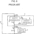
- Fig. 8 illustrates a block diagram of a conventional current output-type detection device.
- the conventional current output-type detection device 1 is composed of: a detection circuit unit 4 composed of a magnetic detection element and the like; and a starting function unit 5 that starts up the detection circuit unit 4.
- an anode side of a power supply source 2 is connected to a power supply terminal Vcc thereof, and a cathode side of the power supply source 2 is connected to a ground terminal Vss thereof through a measuring resistor R.
- a measurement unit 3 is connected in parallel to both ends of the measuring resistor R.
- the starting function unit 5 functions as a constant current source that supplies a constant current In to the detection circuit unit 4, and the starting function unit 5 itself flows a starting current Is therefrom.
- the detection circuit unit 4 starts up by the constant current In supplied from the starting function unit 5, and outputs a detection current Ix that shows a detection result.
- a current consumption I of the detection device 1 becomes a total sum of the starting current Is and the detection current Ix. Therefore, the measurement unit 3 can recognize the detection result by measuring this current consumption I.
- a power supply circuit unit and a current stabilization circuit unit are provided between the starting function unit 5 and the detection circuit unit 4, whereby fluctuation of the current consumption of the detection device, the fluctuation being caused by the variations of the power supply voltage, is suppressed, and the detection device 1 becomes capable of obtaining the detection result with high accuracy.
- current values of the starting current Is and the detection current Ix can be set low, and accordingly, the detection device 1 can reduce an amount of power consumption.
- Patent Document 1 Japanese Patent Application Laid-Open No. 2007-156997
- US 2008/048772 discloses a sensor circuit that has a sensor portion that obtains, as an electrical signal, information on an object to be measured or detected, and a control circuit that controls the operation of the sensor portion.
- the control circuit receives a start input signal inputted thereto from outside for making the sensor portion operate only for a given duration after the start input signal is inputted thereto.
- the current consumption can be reduced by arbitrarily controlling a period of an intermittent operation of the sensor circuit.
- JP 2007-318352 discloses a magnetoelectric transducing switch. When a timing signal from a timing signal generating circuit becomes LOW, the switch is turned OFF, and neither a Hall element nor a binarizing circuit operates. The last output state of the binarizing circuit is held by a latch circuit and the state of a transistor is maintained until the timing signal becomes High next. The Hall element and binarizing circuit are driven only intermittently to contribute to reduction of a mean inter-terminal current.
- JP2007156997 discloses a current output-type detection device according to the state of the art.
- the starting current Is of the starting function unit 5 always flows through the conventional current output-type detection device 1, and accordingly, the conventional current output-type detection device 1 cannot cope with further reduction of the amount of power consumption.
- the present invention has been invented in order to solve such a problem as described above.
- the present invention provides a current output-type detection device capable of reducing the amount of power consumption without sacrificing the detection accuracy.
- a current output-type detection device is defined in claim 1.
- the detection device is configured so that the control circuit 11 can drive the sensor circuit 12 and the sensor signal processing circuit 13 intermittently, and accordingly, the detection device has an effect of being capable of reducing the current consumption without sacrificing the detection accuracy in comparison with the conventional technology.
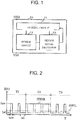
- Fig. 1 is a block diagram illustrating a current output-type detection device 10 of a first embodiment.
- the current output-type detection device 10 of this embodiment includes: a control circuit 11; a sensor circuit 12; and a sensor signal processing circuit 13.
- the control circuit 11 outputs control signals to the sensor circuit 12 and the sensor signal processing circuit 13, and receives a detection signal from the sensor signal processing circuit 13.
- the sensor circuit 12 Upon receiving the control signal from the control circuit 11, the sensor circuit 12 starts up and performs a detection operation.
- the sensor signal processing circuit 13 Upon receiving the control signal from the control circuit 11, the sensor signal processing circuit 13 starts up and outputs a detection signal in response to a detection result of the sensor circuit 12.
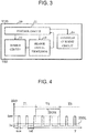
- Fig. 2 is a chart illustrating a relationship between the operations and current consumption of the current output-type detection device 10 of the first embodiment.
- the control circuit 11 includes an oscillation circuit and a counter, outputs the control signals intermittently, and starts up the sensor circuit 12 and the sensor signal processing circuit 13.
- a state that the sensor circuit 12 and the sensor signal processing circuit 13 are stopped is defined as a sleep state tsl
- a state that the sensor circuit 12 and the sensor signal processing circuit 13 are started is defined as an awake state taw.
- Only the control circuit 11 operates in the sleep state tsl, and accordingly, a current consumption of the detection device 10 is a sleep current Isl. All of the circuits operate in the awake state taw, and accordingly, the current consumption of the detection device 10 is an awake current law.
- the period T1 is a non-detection period while a physical quantity to be detected by the sensor circuit 12 does not reach a detection level.
- the sensor circuit 12 does not output the detection signal to the control circuit 11 through the sensor signal processing circuit 13.
- the detection device 10 repeats the sleep state tsl and the awake state taw.
- the current consumption of the detection device 10 is IDDL.
- the period T2 is a detection period while the physical quantity to be detected by the sensor circuit 12 has reached the detection level.
- the sensor circuit 12 outputs the detection signal to the control circuit 11 through the sensor signal processing circuit 13.
- the control circuit 11 outputs the control signals to the sensor circuit 12 and the sensor signal processing circuit 13, and maintains the awake current law.
- the sensor circuit 12 performs an intermittent operation in a similar way to the non-detection period T1.
- the current consumption of the detection device 10 is IDDH.
- the detection device 10 repeats the sleep state tsl and the awake state taw one more time, and the current consumption becomes IDDL.
- Fig. 6 is a block diagram illustrating an example of a sensor system including the current output-type detection device 10 of the present invention.
- the sensor system includes: the detection device 10; a power supply source 2; a measurement unit 3; and a measuring resistor R.
- the measurement unit 3 measures a voltage between both ends of the measuring resistor R, and determines the detection result of the detection device 10.
- the detection device 10 of this embodiment shows the detection result by the current consumption that is as illustrated in Fig. 2 .
- the measurement unit 3 may be configured to determine that the detection signal is outputted, for example, upon measuring that the voltage is a detection voltage VDDH during a fixed period.
- the detection voltage VDDH is a voltage when the awake current law flows through the measuring resistor R.
- Fig. 7 is a block diagram illustrating another example of the sensor system including the current output-type detection device 10 of the present invention.
- the sensor system further includes a filter circuit 6.
- the filter circuit 6 makes a setting so that a waveform of repetition of the sleep current Isl and the awake current law at the time of the non-detection period can be a non-detection current IDDL.
- the measurement unit 3 can determine whether a type of the signal thus received is the detection signal or a non-detection signal based on whether or not the measured voltage is the detection voltage VDDH or a non-detection voltage VDDL.
- the non-detection voltage VDDL is a voltage when the sleep current Isl and the awake current law flow through the measuring resistor R alternately.
- the current output-type detection device 10 of this embodiment is configured so that the control circuit 11 can drive the sensor circuit 12 and the sensor signal processing circuit 13 intermittently, and accordingly, is made capable of reducing the amount of power consumption without sacrificing the detection accuracy in comparison with the conventional technology.
- the current output-type detection device 10 of this embodiment is described as a configuration that intermittently operates in the detection period T2 in a similar way to the non-detection periods T1 and T3, the current output-type detection device 10 of this embodiment may be configured to continuously detect a detection current. In such a way, the current output-type detection device 10 can be turned to a non-detection state early, and accordingly, the current output-type detection device 10 can further reduce the current consumption.
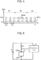
- Fig. 3 is a block diagram illustrating a current output-type detection device 10 of a second embodiment.
- the current output-type detection device 10 of this embodiment includes: a control circuit 11; a sensor circuit 12; a sensor signal processing circuit 13; and a constant current circuit 14.
- the control circuit 11 outputs control signals to the sensor circuit 12, the sensor signal processing circuit 13 and the constant current circuit 14, and receives a detection signal from the sensor signal processing circuit 13.
- the sensor circuit 12 Upon receiving the control signal from the control circuit 11, the sensor circuit 12 starts up and performs a detection operation.
- the sensor signal processing circuit 13 Upon receiving the control signal from the control circuit 11, the sensor signal processing circuit 13 starts up and outputs a detection signal in response to a detection result of the sensor circuit 12.
- the constant current circuit 14 flows a constant current therefrom, and increases a current consumption of the detection device 10.
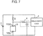
- Fig. 4 is a chart illustrating a relationship between the operations and current consumption of the current output-type detection device 10 of this embodiment.
- the control circuit 11 In the detection period T2, during a period of receiving the detection signal, the control circuit 11 outputs the control signals to the sensor circuit 12 and the sensor signal processing circuit 13, and maintains the awake current law. Moreover, during the period of receiving the detection signal, the control circuit 11 outputs the control signal to the constant current circuit 14. Upon receiving the control signal, the constant current circuit 14 flows a constant current therefrom, and increases the current consumption of the detection device 10.
- the current consumption of the detection device 10 is a current IDDH obtained by adding the constant current of the constant current circuit 14 to the awake current law.
- the current output-type detection device 10 When the current output-type detection device 10 is configured as described above, erroneous detection by the measurement unit 3 decreases, and accordingly, the current consumption of the sensor system is reduced, and in addition, reliability thereof is enhanced.
- the current output-type detection device 10 of this embodiment is described as a configuration that intermittently operates in the detection period T2 in a similar way to the non-detection periods T1 and T3, the current output-type detection device 10 of this embodiment may be configured to continuously detect the detection current. In such a way, the current output-type detection device 10 can be turned to the non-detection state early, and accordingly, the current output-type detection device 10 can reduce the current consumption.
- Fig. 5 is a chart illustrating another example of the relationship between the operations and current consumption of the current output-type detection device 10 of this embodiment.
- the control circuit 11 In the detection period T2, for example, during the period of receiving the detection signal, the control circuit 11 outputs the control signal only to the sensor circuit 12, and flows only the current of the sensor circuit 12. Moreover, during the period of receiving the detection signal, the control circuit 11 outputs the control signal to the constant current circuit 14. Hence, the current consumption of the detection device 10 is the current IDDH obtained by adding the constant current of the constant current circuit 14 to the current of the sensor circuit 12.
- the current consumption of the sensor system can be further reduced.
- the current consumption can be reduced in comparison with the conventional technology.
- the detection current IDDH and the non-detection current IDDL in response to a capability of the measurement unit 3, and accordingly, the current consumption of the sensor system can be reduced, and the reliability thereof can be enhanced.
- the current output-type detection device 10 of the present invention is described as a configuration that flows the current IDDH as the detection current in the detection period T2, the current IDDL may be used as the detection current. In such a way, the current consumption can be reduced in a case of a system in which the detection period is long and the non-detection period is short.
Landscapes
- Physics & Mathematics (AREA)
- General Physics & Mathematics (AREA)
- Condensed Matter Physics & Semiconductors (AREA)
- Measurement Of Current Or Voltage (AREA)
- Arrangements For Transmission Of Measured Signals (AREA)
- Testing Or Calibration Of Command Recording Devices (AREA)
Description
- The present invention relates to a current output-type detection device that changes an amount of current consumption of the device itself in response to a detection result.
- For example, in a current output-type detection device that changes an amount of current consumption of the device itself in response to a detection result of a magnetic sensor or the like, it is important, while suppressing an increase of an amount of power consumption, to suppress lowering of detection accuracy even if variations occur in a power supply voltage (for example, refer to Patent Document 1).
-
Fig. 8 illustrates a block diagram of a conventional current output-type detection device. The conventional current output-type detection device 1 is composed of: a detection circuit unit 4 composed of a magnetic detection element and the like; and a starting function unit 5 that starts up the detection circuit unit 4. In the detection device 1, an anode side of apower supply source 2 is connected to a power supply terminal Vcc thereof, and a cathode side of thepower supply source 2 is connected to a ground terminal Vss thereof through a measuring resistor R.A measurement unit 3 is connected in parallel to both ends of the measuring resistor R. - The starting function unit 5 functions as a constant current source that supplies a constant current In to the detection circuit unit 4, and the starting function unit 5 itself flows a starting current Is therefrom. The detection circuit unit 4 starts up by the constant current In supplied from the starting function unit 5, and outputs a detection current Ix that shows a detection result. Hence, a current consumption I of the detection device 1 becomes a total sum of the starting current Is and the detection current Ix. Therefore, the
measurement unit 3 can recognize the detection result by measuring this current consumption I. - Here, with regard to the detection device 1, a power supply circuit unit and a current stabilization circuit unit are provided between the starting function unit 5 and the detection circuit unit 4, whereby fluctuation of the current consumption of the detection device, the fluctuation being caused by the variations of the power supply voltage, is suppressed, and the detection device 1 becomes capable of obtaining the detection result with high accuracy. Hence, current values of the starting current Is and the detection current Ix can be set low, and accordingly, the detection device 1 can reduce an amount of power consumption.
- [Patent Document 1] Japanese Patent Application Laid-Open No.
2007-156997 -
US 2008/048772 discloses a sensor circuit that has a sensor portion that obtains, as an electrical signal, information on an object to be measured or detected, and a control circuit that controls the operation of the sensor portion. The control circuit receives a start input signal inputted thereto from outside for making the sensor portion operate only for a given duration after the start input signal is inputted thereto. The current consumption can be reduced by arbitrarily controlling a period of an intermittent operation of the sensor circuit. -
JP 2007-318352 - The document
JP2007156997 - However, the starting current Is of the starting function unit 5 always flows through the conventional current output-type detection device 1, and accordingly, the conventional current output-type detection device 1 cannot cope with further reduction of the amount of power consumption.
- The present invention has been invented in order to solve such a problem as described above. The present invention provides a current output-type detection device capable of reducing the amount of power consumption without sacrificing the detection accuracy.
- A current output-type detection device according to an aspect of the present invention is defined in claim 1.
- In accordance with the current output-type detection device of the present invention, the detection device is configured so that the
control circuit 11 can drive thesensor circuit 12 and the sensorsignal processing circuit 13 intermittently, and accordingly, the detection device has an effect of being capable of reducing the current consumption without sacrificing the detection accuracy in comparison with the conventional technology. -
-
Fig. 1 is a block diagram illustrating a current output-type detection device of a first embodiment. -
Fig. 2 is a chart illustrating a relationship between operations and current consumption of the current output-type detection device of the first embodiment. -
Fig. 3 is a block diagram illustrating a current output-type detection device of a second embodiment. -
Fig. 4 is a chart illustrating an example of a relationship between operations and current consumption of the current output-type detection device of the second embodiment. -
Fig. 5 is a chart illustrating another example of the relationship between the operations and current consumption of the current output-type detection device of the second embodiment. -
Fig. 6 is a block diagram illustrating an example of a sensor system including the current output-type detection device of the present invention. -
Fig. 7 is a block diagram illustrating another example of the sensor system including the current output-type detection device of the present invention. -
Fig. 8 is a block diagram illustrating a conventional current output-type detection device. - A description is made below of a current output-type detection device of the present invention with reference to the drawings.
-
Fig. 1 is a block diagram illustrating a current output-type detection device 10 of a first embodiment. - The current output-
type detection device 10 of this embodiment includes: acontrol circuit 11; asensor circuit 12; and a sensorsignal processing circuit 13. - The
control circuit 11 outputs control signals to thesensor circuit 12 and the sensorsignal processing circuit 13, and receives a detection signal from the sensorsignal processing circuit 13. Upon receiving the control signal from thecontrol circuit 11, thesensor circuit 12 starts up and performs a detection operation. Upon receiving the control signal from thecontrol circuit 11, the sensorsignal processing circuit 13 starts up and outputs a detection signal in response to a detection result of thesensor circuit 12. - Next, a description is made of operations of the current output-type detection device of this embodiment.
Fig. 2 is a chart illustrating a relationship between the operations and current consumption of the current output-type detection device 10 of the first embodiment. - For example, the
control circuit 11 includes an oscillation circuit and a counter, outputs the control signals intermittently, and starts up thesensor circuit 12 and the sensorsignal processing circuit 13. A state that thesensor circuit 12 and the sensorsignal processing circuit 13 are stopped is defined as a sleep state tsl, and a state that thesensor circuit 12 and the sensorsignal processing circuit 13 are started is defined as an awake state taw. Only thecontrol circuit 11 operates in the sleep state tsl, and accordingly, a current consumption of thedetection device 10 is a sleep current Isl. All of the circuits operate in the awake state taw, and accordingly, the current consumption of thedetection device 10 is an awake current law. - The period T1 is a non-detection period while a physical quantity to be detected by the
sensor circuit 12 does not reach a detection level. Thesensor circuit 12 does not output the detection signal to thecontrol circuit 11 through the sensorsignal processing circuit 13. Hence, thedetection device 10 repeats the sleep state tsl and the awake state taw. In this non-detection period T1, the current consumption of thedetection device 10 is IDDL. - The period T2 is a detection period while the physical quantity to be detected by the
sensor circuit 12 has reached the detection level. Thesensor circuit 12 outputs the detection signal to thecontrol circuit 11 through the sensorsignal processing circuit 13. During a period of receiving the detection signal, thecontrol circuit 11 outputs the control signals to thesensor circuit 12 and the sensorsignal processing circuit 13, and maintains the awake current law. At this time, thesensor circuit 12 performs an intermittent operation in a similar way to the non-detection period T1. In this detection period T2, the current consumption of thedetection device 10 is IDDH. - In a non-detection period T3 while the physical quantity to be detected by the
sensor circuit 12 has no longer reached the detection level, thedetection device 10 repeats the sleep state tsl and the awake state taw one more time, and the current consumption becomes IDDL. -
Fig. 6 is a block diagram illustrating an example of a sensor system including the current output-type detection device 10 of the present invention. The sensor system includes: thedetection device 10; apower supply source 2; ameasurement unit 3; and a measuring resistor R. Themeasurement unit 3 measures a voltage between both ends of the measuring resistor R, and determines the detection result of thedetection device 10. Thedetection device 10 of this embodiment shows the detection result by the current consumption that is as illustrated inFig. 2 . Accordingly, themeasurement unit 3 may be configured to determine that the detection signal is outputted, for example, upon measuring that the voltage is a detection voltage VDDH during a fixed period. The detection voltage VDDH is a voltage when the awake current law flows through the measuring resistor R. -
Fig. 7 is a block diagram illustrating another example of the sensor system including the current output-type detection device 10 of the present invention. The sensor system further includes afilter circuit 6. Thefilter circuit 6 makes a setting so that a waveform of repetition of the sleep current Isl and the awake current law at the time of the non-detection period can be a non-detection current IDDL. Hence, themeasurement unit 3 can determine whether a type of the signal thus received is the detection signal or a non-detection signal based on whether or not the measured voltage is the detection voltage VDDH or a non-detection voltage VDDL. The non-detection voltage VDDL is a voltage when the sleep current Isl and the awake current law flow through the measuring resistor R alternately. - As described above, the current output-
type detection device 10 of this embodiment is configured so that thecontrol circuit 11 can drive thesensor circuit 12 and the sensorsignal processing circuit 13 intermittently, and accordingly, is made capable of reducing the amount of power consumption without sacrificing the detection accuracy in comparison with the conventional technology. - Note that, though the current output-
type detection device 10 of this embodiment is described as a configuration that intermittently operates in the detection period T2 in a similar way to the non-detection periods T1 and T3, the current output-type detection device 10 of this embodiment may be configured to continuously detect a detection current. In such a way, the current output-type detection device 10 can be turned to a non-detection state early, and accordingly, the current output-type detection device 10 can further reduce the current consumption. -
Fig. 3 is a block diagram illustrating a current output-type detection device 10 of a second embodiment. - The current output-
type detection device 10 of this embodiment includes: acontrol circuit 11; asensor circuit 12; a sensorsignal processing circuit 13; and a constantcurrent circuit 14. - The
control circuit 11 outputs control signals to thesensor circuit 12, the sensorsignal processing circuit 13 and the constantcurrent circuit 14, and receives a detection signal from the sensorsignal processing circuit 13. Upon receiving the control signal from thecontrol circuit 11, thesensor circuit 12 starts up and performs a detection operation. Upon receiving the control signal from thecontrol circuit 11, the sensorsignal processing circuit 13 starts up and outputs a detection signal in response to a detection result of thesensor circuit 12. Upon receiving the control signal, the constantcurrent circuit 14 flows a constant current therefrom, and increases a current consumption of thedetection device 10. - Next, a description is made of operations of the current output-type detection device of this embodiment.
-
Fig. 4 is a chart illustrating a relationship between the operations and current consumption of the current output-type detection device 10 of this embodiment. - Operations of the
detection device 10 in the non-detection period T1 are similar to those of the first embodiment. - In the detection period T2, during a period of receiving the detection signal, the
control circuit 11 outputs the control signals to thesensor circuit 12 and the sensorsignal processing circuit 13, and maintains the awake current law. Moreover, during the period of receiving the detection signal, thecontrol circuit 11 outputs the control signal to the constantcurrent circuit 14. Upon receiving the control signal, the constantcurrent circuit 14 flows a constant current therefrom, and increases the current consumption of thedetection device 10. The current consumption of thedetection device 10 is a current IDDH obtained by adding the constant current of the constantcurrent circuit 14 to the awake current law. - When the current output-
type detection device 10 is configured as described above, erroneous detection by themeasurement unit 3 decreases, and accordingly, the current consumption of the sensor system is reduced, and in addition, reliability thereof is enhanced. - Note that, though the current output-
type detection device 10 of this embodiment is described as a configuration that intermittently operates in the detection period T2 in a similar way to the non-detection periods T1 and T3, the current output-type detection device 10 of this embodiment may be configured to continuously detect the detection current. In such a way, the current output-type detection device 10 can be turned to the non-detection state early, and accordingly, the current output-type detection device 10 can reduce the current consumption. -
Fig. 5 is a chart illustrating another example of the relationship between the operations and current consumption of the current output-type detection device 10 of this embodiment. - Operations of the
detection device 10 in the non-detection period T1 are similar to those of the first embodiment. - In the detection period T2, for example, during the period of receiving the detection signal, the
control circuit 11 outputs the control signal only to thesensor circuit 12, and flows only the current of thesensor circuit 12. Moreover, during the period of receiving the detection signal, thecontrol circuit 11 outputs the control signal to the constantcurrent circuit 14. Hence, the current consumption of thedetection device 10 is the current IDDH obtained by adding the constant current of the constantcurrent circuit 14 to the current of thesensor circuit 12. - When the current output-
type detection device 10 is configured as described above, the current consumption of the sensor system can be further reduced. - As described above, in accordance with the current output-
type detection device 10 of the present invention, the current consumption can be reduced in comparison with the conventional technology. - Moreover, it is possible to set the detection current IDDH and the non-detection current IDDL in response to a capability of the
measurement unit 3, and accordingly, the current consumption of the sensor system can be reduced, and the reliability thereof can be enhanced. - Note that, though the current output-
type detection device 10 of the present invention is described as a configuration that flows the current IDDH as the detection current in the detection period T2, the current IDDL may be used as the detection current. In such a way, the current consumption can be reduced in a case of a system in which the detection period is long and the non-detection period is short. -
- 2
- power supply source
- 3
- measurement unit
- 6
- filter circuit
- 10
- detection device
- 11
- control circuit
- 12
- sensor circuit
- 13
- sensor signal processing circuit
- 14
- constant current circuit
Claims (3)
- A current output-type detection device (10) that changes an amount of current consumption of the device itself in response to a detection result, the detection device (10) comprising:a sensor circuit (12) that detects a physical quantity to be detected;a sensor signal processing circuit (13) that outputs a detection signal upon receiving a signal of a detection result from the sensor circuit (12); and characterized bya control circuit (11) that outputs control signals to the sensor circuit (12) and the sensor signal processing circuit (13) and receives the detection signal from the sensor signal processing circuit (13),wherein the sensor circuit (12) and the sensor signal processing circuit (13) operate intermittently in response to the control signals,wherein, during a period (T1) in which the sensor signal processing circuit (13) does not output the detection signal to the control circuit (11), the control circuit (11) controls the sensor circuit (12) and the sensor signal processing circuit (13) to repeat a sleep state (tsl) in which the circuits are inactive and an awake state (taw) in which the circuits are active, andwherein during a period (T2) in which the control circuit (11) receives the detection signal from the sensor signal processing circuit (13), the control circuit (11) outputs the control signals to the sensor circuit (12) and the sensor signal processing circuit (13) and maintains an awake current (law) in the detection device (10).
- The detection device (10) according to claim 1, further comprising:a constant current circuit (14),wherein the constant current circuit (14) supplies a constant current in response to the control signal so as to increase a current consumption of the detection device (10).
- The detection device (10) according to either one of claims 1 and 2,
wherein the control circuit (11) outputs the control signal to at least either one of the sensor circuit (12) and the sensor signal processing circuit (13), and increases the current consumption of the detection device (10), during the period (T1) of not receiving the detection signal from the sensor signal processing circuit (13).
Applications Claiming Priority (2)
| Application Number | Priority Date | Filing Date | Title |
|---|---|---|---|
| JP2013212173A JP6322378B2 (en) | 2013-10-09 | 2013-10-09 | Detection device |
| PCT/JP2014/073080 WO2015053012A1 (en) | 2013-10-09 | 2014-09-02 | Detection apparatus |
Publications (3)
| Publication Number | Publication Date |
|---|---|
| EP3056871A1 EP3056871A1 (en) | 2016-08-17 |
| EP3056871A4 EP3056871A4 (en) | 2017-08-23 |
| EP3056871B1 true EP3056871B1 (en) | 2020-10-21 |
Family
ID=52812832
Family Applications (1)
| Application Number | Title | Priority Date | Filing Date |
|---|---|---|---|
| EP14852591.8A Not-in-force EP3056871B1 (en) | 2013-10-09 | 2014-09-02 | Detection apparatus |
Country Status (7)
| Country | Link |
|---|---|
| US (1) | US10006971B2 (en) |
| EP (1) | EP3056871B1 (en) |
| JP (1) | JP6322378B2 (en) |
| KR (1) | KR102178994B1 (en) |
| CN (1) | CN105849508B (en) |
| TW (1) | TWI637150B (en) |
| WO (1) | WO2015053012A1 (en) |
Families Citing this family (1)
| Publication number | Priority date | Publication date | Assignee | Title |
|---|---|---|---|---|
| CN106017538A (en) * | 2016-06-27 | 2016-10-12 | 国网江苏省电力公司盐城供电公司 | Transformer detection apparatus |
Citations (1)
| Publication number | Priority date | Publication date | Assignee | Title |
|---|---|---|---|---|
| JP2007156997A (en) * | 2005-12-07 | 2007-06-21 | Tokai Rika Co Ltd | Electric current output type detection device |
Family Cites Families (7)
| Publication number | Priority date | Publication date | Assignee | Title |
|---|---|---|---|---|
| JP2777372B2 (en) * | 1988-04-08 | 1998-07-16 | シチズン時計株式会社 | Sensor signal processing device |
| JP4925630B2 (en) * | 2005-09-06 | 2012-05-09 | 株式会社アドバンテスト | Test apparatus and test method |
| JP2007318352A (en) * | 2006-05-24 | 2007-12-06 | Asahi Kasei Electronics Co Ltd | Magnetoelectric transducing switch |
| JP2008032424A (en) * | 2006-07-26 | 2008-02-14 | Rohm Co Ltd | Sensor circuit, semiconductor device, electronic equipment |
| JP2009038246A (en) * | 2007-08-02 | 2009-02-19 | Rohm Co Ltd | Electronic instrument |
| EP2282175A3 (en) * | 2009-08-06 | 2011-10-19 | Yokogawa Electric Corporation | Measurement apparatus |
| JP2012063211A (en) * | 2010-09-15 | 2012-03-29 | Toshiba Corp | Magnetic detection device |
-
2013
- 2013-10-09 JP JP2013212173A patent/JP6322378B2/en active Active
-
2014
- 2014-09-02 EP EP14852591.8A patent/EP3056871B1/en not_active Not-in-force
- 2014-09-02 KR KR1020167009111A patent/KR102178994B1/en not_active Expired - Fee Related
- 2014-09-02 CN CN201480055712.1A patent/CN105849508B/en not_active Expired - Fee Related
- 2014-09-02 WO PCT/JP2014/073080 patent/WO2015053012A1/en not_active Ceased
- 2014-09-11 TW TW103131355A patent/TWI637150B/en not_active IP Right Cessation
-
2016
- 2016-04-06 US US15/091,784 patent/US10006971B2/en not_active Expired - Fee Related
Patent Citations (1)
| Publication number | Priority date | Publication date | Assignee | Title |
|---|---|---|---|---|
| JP2007156997A (en) * | 2005-12-07 | 2007-06-21 | Tokai Rika Co Ltd | Electric current output type detection device |
Also Published As
| Publication number | Publication date |
|---|---|
| CN105849508B (en) | 2019-01-11 |
| TWI637150B (en) | 2018-10-01 |
| TW201527718A (en) | 2015-07-16 |
| KR102178994B1 (en) | 2020-11-16 |
| WO2015053012A1 (en) | 2015-04-16 |
| EP3056871A4 (en) | 2017-08-23 |
| KR20160067856A (en) | 2016-06-14 |
| EP3056871A1 (en) | 2016-08-17 |
| US10006971B2 (en) | 2018-06-26 |
| CN105849508A (en) | 2016-08-10 |
| JP6322378B2 (en) | 2018-05-09 |
| JP2015075949A (en) | 2015-04-20 |
| US20160216339A1 (en) | 2016-07-28 |
Similar Documents
| Publication | Publication Date | Title |
|---|---|---|
| EP1045251A2 (en) | Voltage detecting circuit | |
| KR101861370B1 (en) | Temperature detection device | |
| KR102105034B1 (en) | Magnetic sensor circuit | |
| CN102692258B (en) | Circuit device, integrated circuit and detection device | |
| US10018685B2 (en) | Method for operating a magnetic field detector circuit and a magnetic field detector circuit | |
| JP2016169962A (en) | Electromagnetic flowmeter | |
| US10006971B2 (en) | Detection device | |
| JP2016027315A (en) | Magnetic sensor device | |
| US20150026502A1 (en) | Reset signal control apparatus | |
| KR102227589B1 (en) | Power supply voltage monitoring circuit, and electronic circuit including the power supply voltage monitoring circuit | |
| JP4229634B2 (en) | Magnetic field strength detector | |
| JP2017017719A (en) | Detection device | |
| US10924050B2 (en) | Motor control circuit and motor controller | |
| CN104009737B (en) | Oscillation-stop detection circuit and electronic equipment | |
| JP2007318352A (en) | Magnetoelectric transducing switch | |
| JPH06174504A (en) | Magnetic detection circuit | |
| JPH11266148A (en) | Voltage detection circuit | |
| JP5806604B2 (en) | Magnetic field detection circuit | |
| JP2016121909A (en) | Detector | |
| JP2019078731A (en) | Controller and sensor module | |
| JP2015070313A (en) | Oscillator |
Legal Events
| Date | Code | Title | Description |
|---|---|---|---|
| PUAI | Public reference made under article 153(3) epc to a published international application that has entered the european phase |
Free format text: ORIGINAL CODE: 0009012 |
|
| 17P | Request for examination filed |
Effective date: 20160509 |
|
| AK | Designated contracting states |
Kind code of ref document: A1 Designated state(s): AL AT BE BG CH CY CZ DE DK EE ES FI FR GB GR HR HU IE IS IT LI LT LU LV MC MK MT NL NO PL PT RO RS SE SI SK SM TR |
|
| AX | Request for extension of the european patent |
Extension state: BA ME |
|
| DAX | Request for extension of the european patent (deleted) | ||
| RIN1 | Information on inventor provided before grant (corrected) |
Inventor name: ARIYAMA, MINORU |
|
| A4 | Supplementary search report drawn up and despatched |
Effective date: 20170720 |
|
| RIC1 | Information provided on ipc code assigned before grant |
Ipc: G01D 3/10 20060101ALI20170714BHEP Ipc: G01D 21/00 20060101AFI20170714BHEP |
|
| RAP1 | Party data changed (applicant data changed or rights of an application transferred) |
Owner name: ABLIC INC. |
|
| STAA | Information on the status of an ep patent application or granted ep patent |
Free format text: STATUS: EXAMINATION IS IN PROGRESS |
|
| 17Q | First examination report despatched |
Effective date: 20180725 |
|
| GRAP | Despatch of communication of intention to grant a patent |
Free format text: ORIGINAL CODE: EPIDOSNIGR1 |
|
| STAA | Information on the status of an ep patent application or granted ep patent |
Free format text: STATUS: GRANT OF PATENT IS INTENDED |
|
| INTG | Intention to grant announced |
Effective date: 20200515 |
|
| GRAS | Grant fee paid |
Free format text: ORIGINAL CODE: EPIDOSNIGR3 |
|
| GRAA | (expected) grant |
Free format text: ORIGINAL CODE: 0009210 |
|
| STAA | Information on the status of an ep patent application or granted ep patent |
Free format text: STATUS: THE PATENT HAS BEEN GRANTED |
|
| AK | Designated contracting states |
Kind code of ref document: B1 Designated state(s): AL AT BE BG CH CY CZ DE DK EE ES FI FR GB GR HR HU IE IS IT LI LT LU LV MC MK MT NL NO PL PT RO RS SE SI SK SM TR |
|
| REG | Reference to a national code |
Ref country code: GB Ref legal event code: FG4D |
|
| REG | Reference to a national code |
Ref country code: CH Ref legal event code: EP |
|
| REG | Reference to a national code |
Ref country code: IE Ref legal event code: FG4D |
|
| REG | Reference to a national code |
Ref country code: DE Ref legal event code: R096 Ref document number: 602014071539 Country of ref document: DE |
|
| REG | Reference to a national code |
Ref country code: AT Ref legal event code: REF Ref document number: 1326277 Country of ref document: AT Kind code of ref document: T Effective date: 20201115 |
|
| REG | Reference to a national code |
Ref country code: AT Ref legal event code: MK05 Ref document number: 1326277 Country of ref document: AT Kind code of ref document: T Effective date: 20201021 |
|
| REG | Reference to a national code |
Ref country code: NL Ref legal event code: MP Effective date: 20201021 |
|
| PG25 | Lapsed in a contracting state [announced via postgrant information from national office to epo] |
Ref country code: PT Free format text: LAPSE BECAUSE OF FAILURE TO SUBMIT A TRANSLATION OF THE DESCRIPTION OR TO PAY THE FEE WITHIN THE PRESCRIBED TIME-LIMIT Effective date: 20210222 Ref country code: NO Free format text: LAPSE BECAUSE OF FAILURE TO SUBMIT A TRANSLATION OF THE DESCRIPTION OR TO PAY THE FEE WITHIN THE PRESCRIBED TIME-LIMIT Effective date: 20210121 Ref country code: NL Free format text: LAPSE BECAUSE OF FAILURE TO SUBMIT A TRANSLATION OF THE DESCRIPTION OR TO PAY THE FEE WITHIN THE PRESCRIBED TIME-LIMIT Effective date: 20201021 Ref country code: FI Free format text: LAPSE BECAUSE OF FAILURE TO SUBMIT A TRANSLATION OF THE DESCRIPTION OR TO PAY THE FEE WITHIN THE PRESCRIBED TIME-LIMIT Effective date: 20201021 Ref country code: RS Free format text: LAPSE BECAUSE OF FAILURE TO SUBMIT A TRANSLATION OF THE DESCRIPTION OR TO PAY THE FEE WITHIN THE PRESCRIBED TIME-LIMIT Effective date: 20201021 Ref country code: GR Free format text: LAPSE BECAUSE OF FAILURE TO SUBMIT A TRANSLATION OF THE DESCRIPTION OR TO PAY THE FEE WITHIN THE PRESCRIBED TIME-LIMIT Effective date: 20210122 |
|
| REG | Reference to a national code |
Ref country code: LT Ref legal event code: MG4D |
|
| PG25 | Lapsed in a contracting state [announced via postgrant information from national office to epo] |
Ref country code: PL Free format text: LAPSE BECAUSE OF FAILURE TO SUBMIT A TRANSLATION OF THE DESCRIPTION OR TO PAY THE FEE WITHIN THE PRESCRIBED TIME-LIMIT Effective date: 20201021 Ref country code: IS Free format text: LAPSE BECAUSE OF FAILURE TO SUBMIT A TRANSLATION OF THE DESCRIPTION OR TO PAY THE FEE WITHIN THE PRESCRIBED TIME-LIMIT Effective date: 20210221 Ref country code: SE Free format text: LAPSE BECAUSE OF FAILURE TO SUBMIT A TRANSLATION OF THE DESCRIPTION OR TO PAY THE FEE WITHIN THE PRESCRIBED TIME-LIMIT Effective date: 20201021 Ref country code: LV Free format text: LAPSE BECAUSE OF FAILURE TO SUBMIT A TRANSLATION OF THE DESCRIPTION OR TO PAY THE FEE WITHIN THE PRESCRIBED TIME-LIMIT Effective date: 20201021 Ref country code: BG Free format text: LAPSE BECAUSE OF FAILURE TO SUBMIT A TRANSLATION OF THE DESCRIPTION OR TO PAY THE FEE WITHIN THE PRESCRIBED TIME-LIMIT Effective date: 20210121 Ref country code: AT Free format text: LAPSE BECAUSE OF FAILURE TO SUBMIT A TRANSLATION OF THE DESCRIPTION OR TO PAY THE FEE WITHIN THE PRESCRIBED TIME-LIMIT Effective date: 20201021 Ref country code: ES Free format text: LAPSE BECAUSE OF FAILURE TO SUBMIT A TRANSLATION OF THE DESCRIPTION OR TO PAY THE FEE WITHIN THE PRESCRIBED TIME-LIMIT Effective date: 20201021 |
|
| PG25 | Lapsed in a contracting state [announced via postgrant information from national office to epo] |
Ref country code: HR Free format text: LAPSE BECAUSE OF FAILURE TO SUBMIT A TRANSLATION OF THE DESCRIPTION OR TO PAY THE FEE WITHIN THE PRESCRIBED TIME-LIMIT Effective date: 20201021 |
|
| REG | Reference to a national code |
Ref country code: DE Ref legal event code: R097 Ref document number: 602014071539 Country of ref document: DE |
|
| PG25 | Lapsed in a contracting state [announced via postgrant information from national office to epo] |
Ref country code: SM Free format text: LAPSE BECAUSE OF FAILURE TO SUBMIT A TRANSLATION OF THE DESCRIPTION OR TO PAY THE FEE WITHIN THE PRESCRIBED TIME-LIMIT Effective date: 20201021 Ref country code: EE Free format text: LAPSE BECAUSE OF FAILURE TO SUBMIT A TRANSLATION OF THE DESCRIPTION OR TO PAY THE FEE WITHIN THE PRESCRIBED TIME-LIMIT Effective date: 20201021 Ref country code: CZ Free format text: LAPSE BECAUSE OF FAILURE TO SUBMIT A TRANSLATION OF THE DESCRIPTION OR TO PAY THE FEE WITHIN THE PRESCRIBED TIME-LIMIT Effective date: 20201021 Ref country code: SK Free format text: LAPSE BECAUSE OF FAILURE TO SUBMIT A TRANSLATION OF THE DESCRIPTION OR TO PAY THE FEE WITHIN THE PRESCRIBED TIME-LIMIT Effective date: 20201021 Ref country code: RO Free format text: LAPSE BECAUSE OF FAILURE TO SUBMIT A TRANSLATION OF THE DESCRIPTION OR TO PAY THE FEE WITHIN THE PRESCRIBED TIME-LIMIT Effective date: 20201021 Ref country code: LT Free format text: LAPSE BECAUSE OF FAILURE TO SUBMIT A TRANSLATION OF THE DESCRIPTION OR TO PAY THE FEE WITHIN THE PRESCRIBED TIME-LIMIT Effective date: 20201021 |
|
| PLBE | No opposition filed within time limit |
Free format text: ORIGINAL CODE: 0009261 |
|
| STAA | Information on the status of an ep patent application or granted ep patent |
Free format text: STATUS: NO OPPOSITION FILED WITHIN TIME LIMIT |
|
| PG25 | Lapsed in a contracting state [announced via postgrant information from national office to epo] |
Ref country code: DK Free format text: LAPSE BECAUSE OF FAILURE TO SUBMIT A TRANSLATION OF THE DESCRIPTION OR TO PAY THE FEE WITHIN THE PRESCRIBED TIME-LIMIT Effective date: 20201021 |
|
| 26N | No opposition filed |
Effective date: 20210722 |
|
| PG25 | Lapsed in a contracting state [announced via postgrant information from national office to epo] |
Ref country code: IT Free format text: LAPSE BECAUSE OF FAILURE TO SUBMIT A TRANSLATION OF THE DESCRIPTION OR TO PAY THE FEE WITHIN THE PRESCRIBED TIME-LIMIT Effective date: 20201021 Ref country code: AL Free format text: LAPSE BECAUSE OF FAILURE TO SUBMIT A TRANSLATION OF THE DESCRIPTION OR TO PAY THE FEE WITHIN THE PRESCRIBED TIME-LIMIT Effective date: 20201021 |
|
| PG25 | Lapsed in a contracting state [announced via postgrant information from national office to epo] |
Ref country code: SI Free format text: LAPSE BECAUSE OF FAILURE TO SUBMIT A TRANSLATION OF THE DESCRIPTION OR TO PAY THE FEE WITHIN THE PRESCRIBED TIME-LIMIT Effective date: 20201021 |
|
| REG | Reference to a national code |
Ref country code: DE Ref legal event code: R119 Ref document number: 602014071539 Country of ref document: DE |
|
| REG | Reference to a national code |
Ref country code: CH Ref legal event code: PL |
|
| REG | Reference to a national code |
Ref country code: BE Ref legal event code: MM Effective date: 20210930 |
|
| GBPC | Gb: european patent ceased through non-payment of renewal fee |
Effective date: 20210902 |
|
| PG25 | Lapsed in a contracting state [announced via postgrant information from national office to epo] |
Ref country code: IS Free format text: LAPSE BECAUSE OF FAILURE TO SUBMIT A TRANSLATION OF THE DESCRIPTION OR TO PAY THE FEE WITHIN THE PRESCRIBED TIME-LIMIT Effective date: 20210221 Ref country code: MC Free format text: LAPSE BECAUSE OF FAILURE TO SUBMIT A TRANSLATION OF THE DESCRIPTION OR TO PAY THE FEE WITHIN THE PRESCRIBED TIME-LIMIT Effective date: 20201021 |
|
| PG25 | Lapsed in a contracting state [announced via postgrant information from national office to epo] |
Ref country code: LU Free format text: LAPSE BECAUSE OF NON-PAYMENT OF DUE FEES Effective date: 20210902 Ref country code: IE Free format text: LAPSE BECAUSE OF NON-PAYMENT OF DUE FEES Effective date: 20210902 Ref country code: GB Free format text: LAPSE BECAUSE OF NON-PAYMENT OF DUE FEES Effective date: 20210902 Ref country code: FR Free format text: LAPSE BECAUSE OF NON-PAYMENT OF DUE FEES Effective date: 20210930 Ref country code: DE Free format text: LAPSE BECAUSE OF NON-PAYMENT OF DUE FEES Effective date: 20220401 Ref country code: BE Free format text: LAPSE BECAUSE OF NON-PAYMENT OF DUE FEES Effective date: 20210930 |
|
| PG25 | Lapsed in a contracting state [announced via postgrant information from national office to epo] |
Ref country code: LI Free format text: LAPSE BECAUSE OF NON-PAYMENT OF DUE FEES Effective date: 20210930 Ref country code: CH Free format text: LAPSE BECAUSE OF NON-PAYMENT OF DUE FEES Effective date: 20210930 |
|
| PG25 | Lapsed in a contracting state [announced via postgrant information from national office to epo] |
Ref country code: HU Free format text: LAPSE BECAUSE OF FAILURE TO SUBMIT A TRANSLATION OF THE DESCRIPTION OR TO PAY THE FEE WITHIN THE PRESCRIBED TIME-LIMIT; INVALID AB INITIO Effective date: 20140902 |
|
| PG25 | Lapsed in a contracting state [announced via postgrant information from national office to epo] |
Ref country code: CY Free format text: LAPSE BECAUSE OF FAILURE TO SUBMIT A TRANSLATION OF THE DESCRIPTION OR TO PAY THE FEE WITHIN THE PRESCRIBED TIME-LIMIT Effective date: 20201021 |
|
| PG25 | Lapsed in a contracting state [announced via postgrant information from national office to epo] |
Ref country code: MK Free format text: LAPSE BECAUSE OF FAILURE TO SUBMIT A TRANSLATION OF THE DESCRIPTION OR TO PAY THE FEE WITHIN THE PRESCRIBED TIME-LIMIT Effective date: 20201021 |
|
| PG25 | Lapsed in a contracting state [announced via postgrant information from national office to epo] |
Ref country code: MT Free format text: LAPSE BECAUSE OF FAILURE TO SUBMIT A TRANSLATION OF THE DESCRIPTION OR TO PAY THE FEE WITHIN THE PRESCRIBED TIME-LIMIT Effective date: 20201021 |
|
| PG25 | Lapsed in a contracting state [announced via postgrant information from national office to epo] |
Ref country code: TR Free format text: LAPSE BECAUSE OF FAILURE TO SUBMIT A TRANSLATION OF THE DESCRIPTION OR TO PAY THE FEE WITHIN THE PRESCRIBED TIME-LIMIT Effective date: 20201021 |