EP3051395A1 - Flexible window substrate and flexible display device having the same - Google Patents
Flexible window substrate and flexible display device having the same Download PDFInfo
- Publication number
- EP3051395A1 EP3051395A1 EP16150398.2A EP16150398A EP3051395A1 EP 3051395 A1 EP3051395 A1 EP 3051395A1 EP 16150398 A EP16150398 A EP 16150398A EP 3051395 A1 EP3051395 A1 EP 3051395A1
- Authority
- EP
- European Patent Office
- Prior art keywords
- coating
- window substrate
- layer
- tiles
- base layer
- Prior art date
- Legal status (The legal status is an assumption and is not a legal conclusion. Google has not performed a legal analysis and makes no representation as to the accuracy of the status listed.)
- Withdrawn
Links
Images



Classifications
-
- G—PHYSICS
- G06—COMPUTING OR CALCULATING; COUNTING
- G06F—ELECTRIC DIGITAL DATA PROCESSING
- G06F3/00—Input arrangements for transferring data to be processed into a form capable of being handled by the computer; Output arrangements for transferring data from processing unit to output unit, e.g. interface arrangements
- G06F3/01—Input arrangements or combined input and output arrangements for interaction between user and computer
- G06F3/03—Arrangements for converting the position or the displacement of a member into a coded form
- G06F3/041—Digitisers, e.g. for touch screens or touch pads, characterised by the transducing means
- G06F3/0412—Digitisers structurally integrated in a display
-
- G—PHYSICS
- G06—COMPUTING OR CALCULATING; COUNTING
- G06F—ELECTRIC DIGITAL DATA PROCESSING
- G06F1/00—Details not covered by groups G06F3/00 - G06F13/00 and G06F21/00
- G06F1/16—Constructional details or arrangements
- G06F1/1613—Constructional details or arrangements for portable computers
- G06F1/1633—Constructional details or arrangements of portable computers not specific to the type of enclosures covered by groups G06F1/1615 - G06F1/1626
- G06F1/1637—Details related to the display arrangement, including those related to the mounting of the display in the housing
- G06F1/1652—Details related to the display arrangement, including those related to the mounting of the display in the housing the display being flexible, e.g. mimicking a sheet of paper, or rollable
-
- G—PHYSICS
- G02—OPTICS
- G02F—OPTICAL DEVICES OR ARRANGEMENTS FOR THE CONTROL OF LIGHT BY MODIFICATION OF THE OPTICAL PROPERTIES OF THE MEDIA OF THE ELEMENTS INVOLVED THEREIN; NON-LINEAR OPTICS; FREQUENCY-CHANGING OF LIGHT; OPTICAL LOGIC ELEMENTS; OPTICAL ANALOGUE/DIGITAL CONVERTERS
- G02F1/00—Devices or arrangements for the control of the intensity, colour, phase, polarisation or direction of light arriving from an independent light source, e.g. switching, gating or modulating; Non-linear optics
- G02F1/01—Devices or arrangements for the control of the intensity, colour, phase, polarisation or direction of light arriving from an independent light source, e.g. switching, gating or modulating; Non-linear optics for the control of the intensity, phase, polarisation or colour
- G02F1/13—Devices or arrangements for the control of the intensity, colour, phase, polarisation or direction of light arriving from an independent light source, e.g. switching, gating or modulating; Non-linear optics for the control of the intensity, phase, polarisation or colour based on liquid crystals, e.g. single liquid crystal display cells
- G02F1/133—Constructional arrangements; Operation of liquid crystal cells; Circuit arrangements
- G02F1/1333—Constructional arrangements; Manufacturing methods
- G02F1/133305—Flexible substrates, e.g. plastics, organic film
-
- G—PHYSICS
- G06—COMPUTING OR CALCULATING; COUNTING
- G06F—ELECTRIC DIGITAL DATA PROCESSING
- G06F3/00—Input arrangements for transferring data to be processed into a form capable of being handled by the computer; Output arrangements for transferring data from processing unit to output unit, e.g. interface arrangements
- G06F3/01—Input arrangements or combined input and output arrangements for interaction between user and computer
- G06F3/03—Arrangements for converting the position or the displacement of a member into a coded form
- G06F3/041—Digitisers, e.g. for touch screens or touch pads, characterised by the transducing means
-
- G—PHYSICS
- G06—COMPUTING OR CALCULATING; COUNTING
- G06F—ELECTRIC DIGITAL DATA PROCESSING
- G06F3/00—Input arrangements for transferring data to be processed into a form capable of being handled by the computer; Output arrangements for transferring data from processing unit to output unit, e.g. interface arrangements
- G06F3/01—Input arrangements or combined input and output arrangements for interaction between user and computer
- G06F3/03—Arrangements for converting the position or the displacement of a member into a coded form
- G06F3/041—Digitisers, e.g. for touch screens or touch pads, characterised by the transducing means
- G06F3/044—Digitisers, e.g. for touch screens or touch pads, characterised by the transducing means by capacitive means
- G06F3/0445—Digitisers, e.g. for touch screens or touch pads, characterised by the transducing means by capacitive means using two or more layers of sensing electrodes, e.g. using two layers of electrodes separated by a dielectric layer
-
- G—PHYSICS
- G06—COMPUTING OR CALCULATING; COUNTING
- G06F—ELECTRIC DIGITAL DATA PROCESSING
- G06F3/00—Input arrangements for transferring data to be processed into a form capable of being handled by the computer; Output arrangements for transferring data from processing unit to output unit, e.g. interface arrangements
- G06F3/01—Input arrangements or combined input and output arrangements for interaction between user and computer
- G06F3/03—Arrangements for converting the position or the displacement of a member into a coded form
- G06F3/041—Digitisers, e.g. for touch screens or touch pads, characterised by the transducing means
- G06F3/044—Digitisers, e.g. for touch screens or touch pads, characterised by the transducing means by capacitive means
- G06F3/0446—Digitisers, e.g. for touch screens or touch pads, characterised by the transducing means by capacitive means using a grid-like structure of electrodes in at least two directions, e.g. using row and column electrodes
-
- G—PHYSICS
- G06—COMPUTING OR CALCULATING; COUNTING
- G06F—ELECTRIC DIGITAL DATA PROCESSING
- G06F3/00—Input arrangements for transferring data to be processed into a form capable of being handled by the computer; Output arrangements for transferring data from processing unit to output unit, e.g. interface arrangements
- G06F3/01—Input arrangements or combined input and output arrangements for interaction between user and computer
- G06F3/03—Arrangements for converting the position or the displacement of a member into a coded form
- G06F3/041—Digitisers, e.g. for touch screens or touch pads, characterised by the transducing means
- G06F3/045—Digitisers, e.g. for touch screens or touch pads, characterised by the transducing means using resistive elements, e.g. a single continuous surface or two parallel surfaces put in contact
-
- G—PHYSICS
- G09—EDUCATION; CRYPTOGRAPHY; DISPLAY; ADVERTISING; SEALS
- G09F—DISPLAYING; ADVERTISING; SIGNS; LABELS OR NAME-PLATES; SEALS
- G09F13/00—Illuminated signs; Luminous advertising
- G09F13/04—Signs, boards or panels, illuminated from behind the insignia
- G09F13/0418—Constructional details
- G09F13/0468—Signs, boards or panels with tensioned or flexible display surface
-
- G—PHYSICS
- G09—EDUCATION; CRYPTOGRAPHY; DISPLAY; ADVERTISING; SEALS
- G09F—DISPLAYING; ADVERTISING; SIGNS; LABELS OR NAME-PLATES; SEALS
- G09F9/00—Indicating arrangements for variable information in which the information is built-up on a support by selection or combination of individual elements
- G09F9/30—Indicating arrangements for variable information in which the information is built-up on a support by selection or combination of individual elements in which the desired character or characters are formed by combining individual elements
- G09F9/301—Indicating arrangements for variable information in which the information is built-up on a support by selection or combination of individual elements in which the desired character or characters are formed by combining individual elements flexible foldable or roll-able electronic displays, e.g. thin LCD, OLED
-
- G—PHYSICS
- G06—COMPUTING OR CALCULATING; COUNTING
- G06F—ELECTRIC DIGITAL DATA PROCESSING
- G06F2203/00—Indexing scheme relating to G06F3/00 - G06F3/048
- G06F2203/041—Indexing scheme relating to G06F3/041 - G06F3/045
- G06F2203/04102—Flexible digitiser, i.e. constructional details for allowing the whole digitising part of a device to be flexed or rolled like a sheet of paper
-
- G—PHYSICS
- G06—COMPUTING OR CALCULATING; COUNTING
- G06F—ELECTRIC DIGITAL DATA PROCESSING
- G06F2203/00—Indexing scheme relating to G06F3/00 - G06F3/048
- G06F2203/041—Indexing scheme relating to G06F3/041 - G06F3/045
- G06F2203/04103—Manufacturing, i.e. details related to manufacturing processes specially suited for touch sensitive devices
-
- G—PHYSICS
- G06—COMPUTING OR CALCULATING; COUNTING
- G06F—ELECTRIC DIGITAL DATA PROCESSING
- G06F2203/00—Indexing scheme relating to G06F3/00 - G06F3/048
- G06F2203/041—Indexing scheme relating to G06F3/041 - G06F3/045
- G06F2203/04112—Electrode mesh in capacitive digitiser: electrode for touch sensing is formed of a mesh of very fine, normally metallic, interconnected lines that are almost invisible to see. This provides a quite large but transparent electrode surface, without need for ITO or similar transparent conductive material
Definitions
- the invention relates generally to a display device.
- a display device is a device which visually displays data.
- the display device which is generally one of the output devices of a computer, is a device which enables a user to directly see results processed by the computer with his/her eyes by displaying the results on a screen.
- Types of display devices include cathode ray tubes (CRTs), liquid crystal displays (LCDs), organic light emitting diode displays (OLED displays), electrophoretic displays (EPDs), and the like.
- CTRs cathode ray tubes
- LCDs liquid crystal displays
- OLED displays organic light emitting diode displays
- EPDs electrophoretic displays
- display devices are currently not limited to a function as output devices of the computer but has been variously applied to an application field such as a television receiver, portable communication devices, wearable electronic devices, and the like.
- liquid crystal displays, organic light emitting diode displays, electrophoretic displays, and the like which may be manufactured as a module having a flat panel shape, may have a large area, a thin profile, and reduced weight, and as a result, have taken the lead in the display industry.
- a flexible display device which may be bent, rolled, or stretched as a whole by external force by using a flexible or stretchable material as a material of a substrate, has been developed.
- a touch screen panel has been developed to be able to use an input scheme which may replace input schemes such as a mouse and a keyboard so as to directly input information to a screen using a hand or a pen. Any user may directly perform his/her desired operation while viewing a screen of a the touch screen panel and easily operate the touch screen panel, and therefore the touch screen panel has been evaluated as the most ideal input scheme under a graphical user interface (GUI) environment and has been widely used in various fields such as a control screen of mobile phones, tablet computers, various kinds of medical equipment and an information display for guiding a bank, a government office, a tourist, and main institutions.
- the touch screen panel is used by being combined with a flat panel display, such as a liquid crystal display (LCD) and an organic light emitting diode (OLED) display, or a flexible display device.
- LCD liquid crystal display
- OLED organic light emitting diode
- a window layer positioned at an outermost side of the flexible display device has flexible characteristics, and therefore a surface thereof may be easily damaged due to a contact of a hand or a touch pen.
- the window layer includes a rigid material to prevent the damage to the surface, the flexibility of the display device may be decreased.
- the present invention sets out to provide a flexible display device that has a flexible window substrate capable of being bent or expanded or contracted by external force, but which is resistant to damage.
- a flexible display device including a display panel configured to display an image, a touch screen panel on the display panel, and a window substrate covering the touch screen panel.
- the window substrate may include: a flexible base layer including a first surface facing an outside and a second surface facing the display panel in an opposite direction to the first surface; a first coating layer having hardness higher than that of the base layer and having a plurality of first coating tiles arranged on the first surface of the base layer thereof, at a first gap from each other; and a second coating layer having hardness higher than that of the base layer and having a plurality of second coating tiles arranged on a layer different from the first surface of the base layer thereof, at a second gap from each other, wherein the first gap of the first coating layer at least partially overlaps one of the second coating tiles of the second coating layer.
- the second coating layer may be on the second surface of the base layer.
- the flexible display device may further include: a third coating layer between the first surface and the second surface of the base layer.
- the third coating layer may include a plurality of third coating tiles which are arranged at a third gap from each other.
- the third gap of the third coating layer may at least partially overlap one of the first coating tiles of the first coating layer or one of the second coating tiles of the second coating layer.
- the third coating layer may be of a single body which is formed as one layer.
- the second coating layer may be on a layer between the first surface and the second surface of the base layer.
- the plurality of first coating tiles and second coating tiles may be isolated from each other.
- the plurality of first coating tiles and the plurality of second coating tiles may be each formed in a matrix form.
- a crossing point of lattice type patterns which are formed by the first gap may at least partially overlap one of the second coating tiles; and a crossing point of lattice type patterns which are by the second gap may at least partially overlap one of the first coating tiles.
- the window substrate may be divided into a display area in which an image is displayed and a non-display area which surrounds the display area and the first coating layer may be at an area which corresponds to the display area.
- the plurality of first coating tiles and the plurality of second coating tiles may have different plane shapes from each other.
- the first coating tiles may have plane areas different from those of the second coating tiles.
- a thickness of the first coating tiles or the second coating tiles may be between 10 ⁇ m an 100 ⁇ m.
- a curvature radius of a tip of a touch pen which is used by contacting a surface of the window substrate is set to be r
- a thickness of the first coating tiles is set to be d
- a maximum gap between the first coating tiles adjacent to each other is set to be S
- the maximum gap may satisfy S ⁇ 2 d 2 r - d
- the gap between the first coating tiles adjacent to each other may be between 20 ⁇ m to 200 ⁇ m.
- the first coating tiles and the second coating tiles may have a quadrangular plane shape.
- the second coating tiles may each correspond to the plurality of first coating tiles.
- the first coating tiles may have a quadrangular plane shape and the second coating tiles may have a hexagonal plane shape.
- the second coating tiles may be arranged so that respective corners of three of the hexagonal coating tiles are adjacent to a point.
- a crossing point of lattice type patterns which are formed by the first gap may at least partially overlap one of the second coating tiles; and at least some of the crossing points formed by the second gap may overlap one of the first coating tiles.
- the base layer may include a material selected from the group consisting of elastomer, polyethylene terephthalate (PET), polyethylene naphthalate (PEN), polyimide (PI), polymethyl methacrylate (PMMA), silicone, polyurethane (PU), and combinations thereof.
- PET polyethylene terephthalate
- PEN polyethylene naphthalate
- PI polyimide
- PMMA polymethyl methacrylate
- PU polyurethane
- the first coating tiles or the second coating tiles may include material selected from the group consisting of epoxy, acryl, silicone, polyurethane (PU), graphene, carbon nanotube (CNT), indium tin oxide (ITO), indium zinc oxide (IZO), Si, SiOx, SiNx, and combinations thereof.
- the flexible display device of an embodiment of the invention it is possible to concurrently implement flexibility and high hardness characteristics by forming the plurality of independently segmented coating layers with the high hardness material on the window substrate including the flexible material.
- the first coating layer on the outer surface of the window substrate to include the first coating tiles which are isolated from each other.
- the word “on” means positioning on or below the object portion, but does not essentially mean positioning on the upper side of the object portion based on a gravity direction.
- the word “comprise” and variations such as “comprises” or “comprising”, will be understood to imply the inclusion of stated elements or components but not the exclusion of any other elements or components.
- spatially relative terms such as “beneath”, “below”, “lower”, “under”, “above”, “upper” and the like, may be used herein for ease of description to describe one element or feature's relationship to another element(s) or feature(s) as illustrated in the figures. It will be understood that the spatially relative terms are intended to encompass different orientations of the device in use or in operation, in addition to the orientation depicted in the figures. For example, if the device in the figures is turned over, elements described as “below” or “beneath” or “under” other elements or features would then be oriented “above” the other elements or features. Thus, the example terms “below” and “under” can encompass both an orientation of above and below. The device may be otherwise oriented (e.g., rotated 90 degrees or at other orientations) and the spatially relative descriptors used herein should be interpreted accordingly.
- first, second, third, etc. may be used herein to describe various elements, components, regions, layers, and/or sections, these elements, components, regions, layers and/or sections should not be limited by these terms. These terms are only used to distinguish one element, component, region, layer or section from another element, component, region, layer or section. Thus, a first element, component, region, layer, or section discussed below could be termed a second element, component, region, layer, or section, without departing from the scope of the present invention.
- one element, component, region, layer and/or section is referred to as being "between" two elements, components, regions, layers, and/or sections, it can be the only element, component, region, layer and/or section between the two elements, components, regions, layers, and/or sections, or one or more intervening elements, components, regions, layers, and/or sections may also be present.
- any numerical range recited herein is intended to include all subranges of the same numerical precision subsumed within the recited range.
- a range of "1.0 to 10.0" or “between 1.0 and 10.0” is intended to include all subranges between (and including) the recited minimum value of 1.0 and the recited maximum value of 10.0, that is, having a minimum value equal to or greater than 1.0 and a maximum value equal to or less than 10.0, such as, for example, 2.4 to 7.6.
- Any maximum numerical limitation recited herein is intended to include all lower numerical limitations subsumed therein and any minimum numerical limitation recited in this specification is intended to include ail higher numerical limitations subsumed therein.
- the term "and/or” includes any and all combinations of one or more of the associated listed items. Expressions such as “at least one of,” when preceding a list of elements, modify the entire list of elements and do not modify the individual elements of the list. Further, the use of “may” when describing embodiments of the present invention refers to “one or more embodiments of the present invention.” Also, the term “exemplary” is intended to refer to an example or illustration.
- FIG. 1 is a perspective view illustrating a flexible display device according to an embodiment of the invention.
- a flexible display device 10 has a structure in which a display panel and a touch screen panel are protected by being covered with a window substrate 200, in which the window substrate 200 may be divided into a display area DA for displaying an image and a non-display area ND surrounding the display area DA, and having a driving circuit unit (or a driving circuit, a frame, and the like positioned thereon.
- the window substrate 200 includes a base layer 210 made of a flexible material and a coating layer 230 in which a plurality of coating tiles 231 are arranged on and attached to a surface toward an outside of the base layer 210 at a distance from each other.
- the coating layer 230 is formed by attaching a plurality of coating tiles 231 to the base layer 210 of the window substrate 200 corresponding to at least the display area DA, and the coating tile 231 is made of a material having hardness higher than that of the base layer 210.
- FIG. 2 is a partial cross-sectional view taken along the line II-II of FIG. 1 and FIG. 3 is a cross-sectional view illustrating a window substrate of FIG. 2 .
- FIG. 2 illustrates that a touch screen panel 150 is attached to an upper portion of the display panel 100 and the window substrate 200 is attached to an upper portion of the touch screen panel 150 to cover the display panel 100 and the touch screen panel 150.
- the display panel 100 includes a plurality of pixels which are arranged in a matrix form to display an image, and may be configured of an organic light emitting panel according to an embodiment of the invention.
- the display panel 100 may be formed on a flexible substrate to have flexible characteristics, and therefore, may be configured of a curved panel or a bendable, foldable, rollable, or stretchable panel.
- a lower protective film 120 is provided under the display panel 100 to protect the display panel 100.
- the lower protective film 120 may be formed of a flexible plastic film, for example, polyimide (PI) and/or polyethylene terephthalate (PET).
- a display panel adhesive layer 115 may be interposed between the lower protective film 120 and the display panel 100 to attach the display panel 100 to the lower protective film 120.
- the display panel adhesive layer 115 may be made of an optically clear adhesive (OCA) and may be applied in an adhesive tape form or may also be applied by applying and hardening an adhesive material.
- OCA optically clear adhesive
- An optical film may be attached on the display panel 100.
- the optical film may also be positioned on the touch screen panel 150.
- the optical film may include a polarization film and a phase difference film, in which the polarization film may polarize light incident on the display panel and light obtained by reflecting the incident light from the display panel, and the phase difference film may be adjacently disposed on the display panel rather than on the polarization film to control a phase of the incident light and the reflected light.
- the touch screen panel 150 is attached over the display panel 100.
- the touch screen panel 150 is positioned over the optical film, and a TSP adhesive layer 125 may be interposed between the display panel 100 and the touch screen panel 150 to attach the touch screen panel 150 to the display panel 100.
- the TSP adhesive layer 125 may be made of an optically clear adhesive (OCA) and may be applied in an adhesive tape form or may also be applied by applying and hardening an adhesive material.
- OCA optically clear adhesive
- the touch screen panel 150 may sense a touch position input from the outside, and the window substrate 200 may be positioned over the touch screen panel 150 to sense the touch position generated from the window substrate 200.
- the touch screen panel 150 may be formed of a panel which is driven with a capacitive type but the present invention is not limited thereto, and therefore the touch screen panel 150 may also be formed of a panel which is driven with a resistive film type, an ultrasonic type, and/or an infrared type.
- the window substrate 200 is formed to have an area larger than that of the display panel 100 and the touch screen panel 150 to cover the display panel 100 and the touch screen panel 150.
- the window adhesive layer 175 is interposed between the touch screen panel 150 and the window substrate 200 to attach the window substrate 200 to the touch screen panel 150.
- the window adhesive layer 175 may be made of an optically clear adhesive (OCA) and may be applied in an adhesive tape form or may also be applied by applying and hardening an adhesive material.
- OCA optically clear adhesive
- the window substrate 200 includes the flexible base layer 210 having a first surface 210a facing the outside and a second surface 210b facing the display panel 100 in an opposite direction thereto and the first coating layer 230 in which the plurality of first coating tiles 231 are arranged on and attached to the first surface 210a of the base layer 210 at a first gap s1 from each other.
- the second coating layer 220 in which a plurality of second coating tiles 221 are arranged on and attached to the second surface 210b of the base layer 210 at a second gap s2 from each other is formed.
- the first gap s1 of the first coating layer 230 may be disposed to at least partially overlap the second coating tile 221 of the second coating layer 220.
- the first coating tile 231 and the second coating tile 221 may be made of a material having hardness higher than that of the base layer 210 and may be made of different materials.
- the base layer 210 may be made of a material selected from the group consisting of elastomer, polyethylene terephthalate (PET), polyethylene naphthalate (PEN), polyimide (PI), polymethyl methacrylate (PMMA), silicone, polyurethane (PU), and combinations thereof.
- the first coating tile 231 and the second coating tile 221 may be made of a material selected from the group consisting of epoxy, acryl, silicone, polyurethane (PU), graphene, carbon nanotube (CNT), indium tin oxide (ITO), indium zinc oxide (IZO), Si, SiOx, SiNx, and combinations thereof.
- the first coating layer 230 includes the first coating tiles 231 which are formed to be isolated from each other to maintain the hardness of the surface at a high level while securing the flexibility or stretchability of the window substrate 200.
- the second coating layer 220 includes the second coating tile 221 which is disposed to partially overlap the first gap s1 of the first coating layer 230 to serve to reinforce the hardness of a portion of the first gap s1 through which the base layer 210 is exposed to the outside.
- first coating tile 231 and the second coating tile 221 may be configured to complement each other even though the alignment of the coating tiles is not precisely controlled during the process to promote the hardness of the window substrate and the gap between the coating tiles si covered to improve visibility.
- FIG. 4 is a diagram for describing a gap design condition of a coating tile formed on the window substrate of the flexible display device according to an embodiment of the invention.
- the maximum gap S may be formed to satisfy the following Equation 1. S ⁇ 2 d 2 r - d
- the maximum gap S depending on the curvature radius r of the tip of the touch pen TP is shown in the following Table 1.
- Maximum gap (S) [ ⁇ m] d 10 ⁇ m 0.01 20 0.05 60 0.1 87.2 0.5 199.0 0.7 235.8 1.0 282.1
- the following Table 2 shows a pitch of the first coating tiles 231, a width H of the coating tile 231, and gaps S and S' between the first coating tiles 231 before the window substrate 200 is stretched, after the window substrate 200 is stretched by 30 %, and the window substrate 200 is stretched by 100 %.
- the pitch of the first coating tile 231 may be obtained by a summed value of the width H and the gaps S and S' and the maximum gap before the window substrate 200 is stretched is set to be S and the maximum gap after the window substrate 200 is stretched is set to be S'.
- the width H and the maximum gap S of the first coating tile 231 before the window substrate 200 is stretched are designed to be the same or substantially the same as each other.
- the allowable maximum gap S may be appreciated to be about 199 ⁇ m.
- the case in which the maximum gap S' is set to be 200 ⁇ m when the window substrate 200 is stretched by 30% is the maximum allowable value and the case in which the gap S' is 150 ⁇ m when the window substrate 200 is stretched by 100% is the maximum allowable value.
- the width H and the maximum gap S of the first coating tile 231 may be each set to be up to 125 ⁇ m, and when the elongation of the window substrate 200 is 100%, the width H and the maximum gap S of the first coating tile 231 may be each set to be up to 50 ⁇ m.
- FIG. 5 is a plan view illustrating a coating layer pattern formed on the window substrate of the flexible display device according to an embodiment of the invention.
- the plurality of first coating tiles 231 are each formed to be isolated from each other while having the same or substantially the same plane shape and are attached to the first surface 210a of the base layer 210 while being arranged in a matrix form.
- the plurality of second coating tiles 221 are each formed to be isolated from each other while having the same or substantially the same plane shape, and are attached to the second surface 210b of the base layer 210 while being arranged in the matrix form.
- the first coating tile 231 and the second coating tile 221 each have a square plane shape and the first gap s1 formed between the first coating tiles 231 adjacent to each other and the second gaps s2 formed between the second coating tiles 221 adjacent to each other are arranged to have a uniform gap in all directions on a plane.
- a crossing point s1 of a lattice type pattern which is formed by the first gap s1 is disposed to overlap the second coating tile 221 and a crossing point p2 of the lattice type pattern formed by the second gap s2 is disposed to overlap the first coating tile 231. Therefore, the first gap s1 of the first coating layer 230 partially overlaps the second coating tile 221 of the second coating layer 220, and the second gap s2 of the second coating layer 220 partially overlaps the first coating tile 231 of the first coating layer 230.
- the number and each area of coating tiles 231 and 221 which are included in the first coating layer 230 and the second coating layer 220, respectively, may be determined and selected depending on the size of the display device and the designed flexibility.
- Each of the coating tiles 231 and 221 may be formed at a size to which at least one pixel corresponds, formed to have the same or substantially the same area for each layer, or formed to have the same or substantially the same area in all the layers.
- FIG. 6 is a plan view illustrating a coating layer pattern formed on a window substrate of a flexible display device according to another exemplary embodiment.
- the first coating layer formed on the first surface facing the outside of the window substrate includes the first coating tile 231 having a square plane shape.
- the second coating layer formed on the second surface of the window substrate facing the display panel includes the second coating tile 321 having a rectangular plane shape and the second coating tile 321 is formed to have an area corresponding to the plurality of first coating tiles 231.
- eight first coating tiles 231 may correspond to one second coating tile 321.
- the first gap s1 formed between the first coating tiles 231 adjacent to each other and the second gap s2 formed between the second coating tiles 321 adjacent to each other may be arranged to have a uniform gap in all directions on a plane.
- a portion of the crossing point p1 of the lattice type pattern which is formed by the first gap s1 is disposed to overlap the second coating tile 321. Therefore, the first gap s1 partially overlaps the second coating tile 321 of the second coating layer. However, when the first coating tiles 231 of the first coating layer are arranged to be included in the second coating tile 321 region of the second coating layer, the second gap s2 of the second coating layer may not overlap the first coating tile 231.
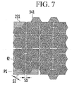
- FIG. 7 is a plan view illustrating a coating layer pattern formed on a window substrate of a flexible display device according to still another embodiment of the invention.
- the first coating layer formed on the first surface facing the outside of the window substrate includes the first coating tile 231 having a quadrangular plane shape.
- the second coating layer which is formed on the second surface of the window substrate facing the display panel includes a second coating tile 341 having a hexagonal plane shape. Corners of each of the second coating tiles 341 having three hexagonal shapes may be disposed to be adjacent to one point (crossing point).
- the first gap s1 formed between the first coating tiles 231 adjacent to each other may be arranged to have a uniform gap in all directions on a plane and the second gap s2 between adjacent sides of each of the second coating tiles 341 adjacent to each other may be uniformly formed over the whole of the second coating layer.
- a portion of the crossing point p1 of the lattice type pattern which is formed by the first gap s1 is disposed to overlap the second coating tile 341 and a portion of a crossing point f2 of the pattern formed by the second gap s2 is disposed to overlap the first coating tile 231. Therefore, the first gap s1 of the first coating layer partially overlaps the second coating tile 341 of the second coating layer and the second gap s2 of the second coating layer partially overlaps the first coating tile 231 of the first coating layer.
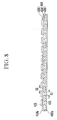
- FIG. 8 is a cross-sectional view illustrating the coating layer pattern formed on the window substrate of the flexible display device according to still another embodiment of the invention.
- a window substrate 400 includes the flexible base layer 410 having a first surface 410a facing the outside and a second surface 410b facing the display panel (see FIG. 2 ) in an opposite direction thereto, and the first coating layer 420 in which the plurality of first coating tiles 421 are arranged on and attached to the first surface 410a of the base layer 410 at the first gap s1 from each other.
- the second coating layer 430 in which the plurality of second coating tiles 431 are arranged at the second gap s2 is formed on the layer between the first surface 410a and the second surface 410b of the base layer 410. That is, the second coating layer 430 may be positioned inside the base layer 410.
- the first gap s1 of the first coating layer 420 may be disposed to at least partially overlap the second coating tile 431 of the second coating layer 430.
- the first coating tile 421 and the second coating tile 431 may be made of a material having hardness higher than that of the base layer 410 and may be made of different materials.
- the base layer 410 may be made of a material selected from the group consisting of elastomer, polyethylene terephthalate (PET), polyethylene naphthalate (PEN), polyimide (PI), polymethyl methacrylate (PMMA), silicone, polyurethane (PU), and combinations thereof.
- the first coating tile 421 and the second coating tile 431 may be made of a material selected from the group consisting of epoxy, acryl, silicone, polyurethane (PU), graphene, carbon nanotube (CNT), indium tin oxide (ITO), indium zinc oxide (IZO), Si, SiOx, SiNx, and combinations thereof.
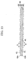
- FIG. 9 is a cross-sectional view illustrating the coating layer pattern formed on the window substrate of the flexible display device according to still another embodiment of the invention.
- a window substrate 450 includes the flexible base layer 410 having a first surface 410a facing the outside and a second surface 410b facing the display panel (see FIG. 2 ) in an opposite direction thereto, and the first coating layer 420 in which the plurality of first coating tiles 421 are arranged on and attached to the first surface 410a of the base layer 410 at the first gap s1 from each other.
- the second coating layer 440 in which the plurality of second coating tiles 441 are arranged at and attached to the second gap s2 from each other is formed on the second surface 410b of the base layer 410, and the third coating layer 430 in which the plurality of third coating tiles 431 are arranged at a third gap s3 is formed on a layer between the first surface 410a and the second surface 410b of the base layer 410. That is, the third coating layer 430 may be positioned inside the base layer 410.
- the first gap s1 of the first coating layer 420 may be disposed to at least partially overlap the second coating tile 441 of the second coating layer 440 or the third coating tile 431 of the third coating layer 430.
- the first coating tile 421, the second coating tile 441, and the third coating tile 431 may be made of a material having hardness higher than that of the base layer 410 and may be made of different materials.
- the base layer 410 may be made of a material selected from the group consisting of elastomer, polyethylene terephthalate (PET), polyethylene naphthalate (PEN), polyimide (PI), polymethyl methacrylate (PMMA), silicone, polyurethane (PU), and combinations thereof.
- the first coating tile 421, the second coating tile 441, and the third coating tile 431 may be made of a material selected from the group consisting of epoxy, acryl, silicone, polyurethane (PU), graphene, carbon nanotube (CNT), indium tin oxide (ITO), indium zinc oxide (IZO), Si, SiOx, SiNx, and combinations thereof.
- FIG. 10 is a cross-sectional view illustrating the coating layer pattern formed on the window substrate of the flexible display device according to still another embodiment of the invention.
- a window substrate 480 includes the flexible base layer 410 having a first surface 410a facing the outside and a second surface 410b facing the display panel (see FIG. 2 ) in an opposite direction thereto, and the first coating layer 420 in which the plurality of first coating tiles 421 are arranged on and attached to the first surface 410a of the base layer 410 at the first gap s1 from each other.
- the second coating layer 440 in which the plurality of second coating tiles 441 are arranged at and attached to the second gap s2 from each other is formed on the second surface 410b of the base layer 410, and a third coating layer 435 having a single layer structure is formed on a layer between the first surface 410a and the second surface 410b of the base layer 410. That is, the third coating layer 435 may be positioned inside the base layer 410 and may be formed as a single body in which the whole of the third coating layer 435 is connected as one layer.
- the first gap s1 of the first coating layer 420 may be disposed to at least partially overlap the second coating tile 441 of the second coating layer 440.
- the first coating tile 421, the second coating tile 441, and the third coating layer 435 may be made of a material having hardness higher than that of the base layer 410 and may be made of different materials.
- the base layer 410 may be made of a material selected from the group consisting of elastomer, polyethylene terephthalate (PET), polyethylene naphthalate (PEN), polyimide (PI), polymethyl methacrylate (PMMA), silicone, polyurethane (PU), and combinations thereof.
- the first coating tile 421, the second coating tile 441, and the third coating layer 435 may be made of a material selected from the group consisting of epoxy, acryl, silicone, polyurethane (PU), graphene, carbon nanotube (CNT), indium tin oxide (ITO), indium zinc oxide (IZO), Si, SiOx, SiNx, and combinations thereof.
Landscapes
- Engineering & Computer Science (AREA)
- Theoretical Computer Science (AREA)
- General Engineering & Computer Science (AREA)
- Physics & Mathematics (AREA)
- General Physics & Mathematics (AREA)
- Human Computer Interaction (AREA)
- Computer Hardware Design (AREA)
- Nonlinear Science (AREA)
- Devices For Indicating Variable Information By Combining Individual Elements (AREA)
- Mathematical Physics (AREA)
- Chemical & Material Sciences (AREA)
- Crystallography & Structural Chemistry (AREA)
- Optics & Photonics (AREA)
- Electroluminescent Light Sources (AREA)
Abstract
Description
- The invention relates generally to a display device.
- A display device is a device which visually displays data. Generally, the display device, which is generally one of the output devices of a computer, is a device which enables a user to directly see results processed by the computer with his/her eyes by displaying the results on a screen. Types of display devices include cathode ray tubes (CRTs), liquid crystal displays (LCDs), organic light emitting diode displays (OLED displays), electrophoretic displays (EPDs), and the like. With recent developments in the field of display devices, display devices are currently not limited to a function as output devices of the computer but has been variously applied to an application field such as a television receiver, portable communication devices, wearable electronic devices, and the like.
- Among the display devices, liquid crystal displays, organic light emitting diode displays, electrophoretic displays, and the like, which may be manufactured as a module having a flat panel shape, may have a large area, a thin profile, and reduced weight, and as a result, have taken the lead in the display industry. Further, a flexible display device, which may be bent, rolled, or stretched as a whole by external force by using a flexible or stretchable material as a material of a substrate, has been developed.
- A touch screen panel has been developed to be able to use an input scheme which may replace input schemes such as a mouse and a keyboard so as to directly input information to a screen using a hand or a pen. Any user may directly perform his/her desired operation while viewing a screen of a the touch screen panel and easily operate the touch screen panel, and therefore the touch screen panel has been evaluated as the most ideal input scheme under a graphical user interface (GUI) environment and has been widely used in various fields such as a control screen of mobile phones, tablet computers, various kinds of medical equipment and an information display for guiding a bank, a government office, a tourist, and main institutions. The touch screen panel is used by being combined with a flat panel display, such as a liquid crystal display (LCD) and an organic light emitting diode (OLED) display, or a flexible display device.
- Although the touch screen panel is applied to the flexible display device, a window layer positioned at an outermost side of the flexible display device has flexible characteristics, and therefore a surface thereof may be easily damaged due to a contact of a hand or a touch pen. When the window layer includes a rigid material to prevent the damage to the surface, the flexibility of the display device may be decreased.
- The above information disclosed in this Background section is only for enhancement of understanding of the background of the described technology and therefore it may contain information that does not form prior art.
- The present invention sets out to provide a flexible display device that has a flexible window substrate capable of being bent or expanded or contracted by external force, but which is resistant to damage.
- According to the present invention there is provided a flexible display device including a display panel configured to display an image, a touch screen panel on the display panel, and a window substrate covering the touch screen panel.
- The window substrate may include: a flexible base layer including a first surface facing an outside and a second surface facing the display panel in an opposite direction to the first surface; a first coating layer having hardness higher than that of the base layer and having a plurality of first coating tiles arranged on the first surface of the base layer thereof, at a first gap from each other; and a second coating layer having hardness higher than that of the base layer and having a plurality of second coating tiles arranged on a layer different from the first surface of the base layer thereof, at a second gap from each other, wherein the first gap of the first coating layer at least partially overlaps one of the second coating tiles of the second coating layer.
- The second coating layer may be on the second surface of the base layer.
- The flexible display device may further include: a third coating layer between the first surface and the second surface of the base layer.
- The third coating layer may include a plurality of third coating tiles which are arranged at a third gap from each other.
- The third gap of the third coating layer may at least partially overlap one of the first coating tiles of the first coating layer or one of the second coating tiles of the second coating layer.
- The third coating layer may be of a single body which is formed as one layer.
- The second coating layer may be on a layer between the first surface and the second surface of the base layer.
- The plurality of first coating tiles and second coating tiles may be isolated from each other.
- The plurality of first coating tiles and the plurality of second coating tiles may be each formed in a matrix form.
- A crossing point of lattice type patterns which are formed by the first gap may at least partially overlap one of the second coating tiles; and a crossing point of lattice type patterns which are by the second gap may at least partially overlap one of the first coating tiles.
- The window substrate may be divided into a display area in which an image is displayed and a non-display area which surrounds the display area and the first coating layer may be at an area which corresponds to the display area.
- The plurality of first coating tiles and the plurality of second coating tiles may have different plane shapes from each other.
- The first coating tiles may have plane areas different from those of the second coating tiles.
- A thickness of the first coating tiles or the second coating tiles may be between 10µm an 100 µm.
- When a curvature radius of a tip of a touch pen which is used by contacting a surface of the window substrate is set to be r, a thickness of the first coating tiles is set to be d, and a maximum gap between the first coating tiles adjacent to each other is set to be S, the maximum gap may satisfy

- The gap between the first coating tiles adjacent to each other may be between 20µm to 200 µm.
- The first coating tiles and the second coating tiles may have a quadrangular plane shape.
- The second coating tiles may each correspond to the plurality of first coating tiles.
- The first coating tiles may have a quadrangular plane shape and the second coating tiles may have a hexagonal plane shape.
- The second coating tiles may be arranged so that respective corners of three of the hexagonal coating tiles are adjacent to a point.
- A crossing point of lattice type patterns which are formed by the first gap may at least partially overlap one of the second coating tiles; and at least some of the crossing points formed by the second gap may overlap one of the first coating tiles.
- The base layer may include a material selected from the group consisting of elastomer, polyethylene terephthalate (PET), polyethylene naphthalate (PEN), polyimide (PI), polymethyl methacrylate (PMMA), silicone, polyurethane (PU), and combinations thereof.
- The first coating tiles or the second coating tiles may include material selected from the group consisting of epoxy, acryl, silicone, polyurethane (PU), graphene, carbon nanotube (CNT), indium tin oxide (ITO), indium zinc oxide (IZO), Si, SiOx, SiNx, and combinations thereof.
- At least some of the above and other features of the invention are set out in the claims.
- As described above, according to the flexible display device of an embodiment of the invention, it is possible to concurrently implement flexibility and high hardness characteristics by forming the plurality of independently segmented coating layers with the high hardness material on the window substrate including the flexible material.
- That is, it is possible to maintain the hardness of the surface at a high level while securing flexibility or stretchability of the window substrate by allowing the first coating layer on the outer surface of the window substrate to include the first coating tiles which are isolated from each other. Further, it is possible to reinforce the hardness of the first gap portion through which the base layer is exposed to the outside by allowing the second coating layer inside the window substrate to include the second coating coil arranged to partially overlap the first gap of the first coating layer.
- Further, it is possible to improve the hardness of the window substrate by configuring the first coating tiles and the second coating tiles in the complementary form to each other even though the alignment of the coating tiles is not precisely controlled during the process and to improve the visibility by covering the gap between the coating tiles.
-
-
FIG. 1 is a perspective view illustrating a flexible display device according to an embodiment of the invention. -
FIG. 2 is a partial cross-sectional view taken along the line II-II ofFIG. 1 . -
FIG. 3 is a cross-sectional view illustrating a window substrate ofFIG. 2 . -
FIG. 4 is a diagram for describing a gap design condition of a coating tile formed on the window substrate of the flexible display device according to an embodiment of the invention. -
FIG. 5 is a plan view illustrating a coating layer pattern formed on the window substrate of the flexible display device according to an embodiment of the invention. -
FIG. 6 is a plan view illustrating a coating layer pattern formed on a window substrate of a flexible display device according to another embodiment of the invention. -
FIG. 7 is a plan view illustrating a coating layer pattern formed on a window substrate of a flexible display device according to still another embodiment of the invention. -
FIG. 8 is a cross-sectional view illustrating the coating layer pattern formed on the window substrate of the flexible display device according to still another embodiment of the invention. -
FIG. 9 is a cross-sectional view illustrating the coating layer pattern formed on the window substrate of the flexible display device according to still another embodiment of the invention. -
FIG. 10 is a cross-sectional view illustrating the coating layer pattern formed on the window substrate of the flexible display device according to still another embodiment of the invention. - In the following detailed description, certain embodiments of the invention have been shown and described, simply by way of illustration. As those skilled in the art would realize, the described embodiments may be modified in various suitableways, all without departing from the scope of the present invention. The drawings and description are to be regarded as illustrative in nature and not restrictive. Like reference numerals designate like elements or components throughout the specification. In addition, the size and thickness of each configuration shown in the drawings are arbitrarily shown for understanding and ease of description, but the present invention is not limited thereto.
- Further, in the specification, the word "on" means positioning on or below the object portion, but does not essentially mean positioning on the upper side of the object portion based on a gravity direction. In addition, unless explicitly described to the contrary, the word "comprise" and variations such as "comprises" or "comprising", will be understood to imply the inclusion of stated elements or components but not the exclusion of any other elements or components.
- Spatially relative terms, such as "beneath", "below", "lower", "under", "above", "upper" and the like, may be used herein for ease of description to describe one element or feature's relationship to another element(s) or feature(s) as illustrated in the figures. It will be understood that the spatially relative terms are intended to encompass different orientations of the device in use or in operation, in addition to the orientation depicted in the figures. For example, if the device in the figures is turned over, elements described as "below" or "beneath" or "under" other elements or features would then be oriented "above" the other elements or features. Thus, the example terms "below" and "under" can encompass both an orientation of above and below. The device may be otherwise oriented (e.g., rotated 90 degrees or at other orientations) and the spatially relative descriptors used herein should be interpreted accordingly.
- It will be understood that, although the terms "first", "second", "third", etc., may be used herein to describe various elements, components, regions, layers, and/or sections, these elements, components, regions, layers and/or sections should not be limited by these terms. These terms are only used to distinguish one element, component, region, layer or section from another element, component, region, layer or section. Thus, a first element, component, region, layer, or section discussed below could be termed a second element, component, region, layer, or section, without departing from the scope of the present invention.
- Further, it will also be understood that when one element, component, region, layer and/or section is referred to as being "between" two elements, components, regions, layers, and/or sections, it can be the only element, component, region, layer and/or section between the two elements, components, regions, layers, and/or sections, or one or more intervening elements, components, regions, layers, and/or sections may also be present.
- The terminology used herein is for the purpose of describing particular embodiments only and is not intended to be limiting of the present invention. As used herein, the singular forms "a" and "an" are intended to include the plural forms as well, unless the context clearly indicates otherwise.
- As used herein, the term "substantially," "about," and similar terms are used as terms of approximation and not as terms of degree, and are intended to account for the inherent deviations in measured or calculated values that would be recognized by those of ordinary skill in the art.
- As used herein, the terms "use," "using," and "used" may be considered synonymous with the terms "utilize," "utilizing," and "utilized," respectively.
- Also, any numerical range recited herein is intended to include all subranges of the same numerical precision subsumed within the recited range. For example, a range of "1.0 to 10.0" or "between 1.0 and 10.0" is intended to include all subranges between (and including) the recited minimum value of 1.0 and the recited maximum value of 10.0, that is, having a minimum value equal to or greater than 1.0 and a maximum value equal to or less than 10.0, such as, for example, 2.4 to 7.6. Any maximum numerical limitation recited herein is intended to include all lower numerical limitations subsumed therein and any minimum numerical limitation recited in this specification is intended to include ail higher numerical limitations subsumed therein. As used herein, the term "and/or" includes any and all combinations of one or more of the associated listed items. Expressions such as "at least one of," when preceding a list of elements, modify the entire list of elements and do not modify the individual elements of the list. Further, the use of "may" when describing embodiments of the present invention refers to "one or more embodiments of the present invention." Also, the term "exemplary" is intended to refer to an example or illustration.
- Hereinafter, a flexible display device according to an embodiment of the invention will be described in detail with the accompanying drawings.
-
FIG. 1 is a perspective view illustrating a flexible display device according to an embodiment of the invention. - Referring to
FIG. 1 , aflexible display device 10 according to an embodiment of the invention has a structure in which a display panel and a touch screen panel are protected by being covered with awindow substrate 200, in which thewindow substrate 200 may be divided into a display area DA for displaying an image and a non-display area ND surrounding the display area DA, and having a driving circuit unit (or a driving circuit, a frame, and the like positioned thereon. Thewindow substrate 200 includes abase layer 210 made of a flexible material and acoating layer 230 in which a plurality ofcoating tiles 231 are arranged on and attached to a surface toward an outside of thebase layer 210 at a distance from each other. - For an input onto the display screen, a user may use a touch pen TP by making the touch pen TP contact a surface of the
window substrate 200. Therefore, thecoating layer 230 is formed by attaching a plurality ofcoating tiles 231 to thebase layer 210 of thewindow substrate 200 corresponding to at least the display area DA, and thecoating tile 231 is made of a material having hardness higher than that of thebase layer 210. -
FIG. 2 is a partial cross-sectional view taken along the line II-II ofFIG. 1 andFIG. 3 is a cross-sectional view illustrating a window substrate ofFIG. 2 . - A cross section configuration of the
flexible display device 10 according to an embodiment of the invention will be described in more detail fromFIG. 2 , which illustrates that atouch screen panel 150 is attached to an upper portion of thedisplay panel 100 and thewindow substrate 200 is attached to an upper portion of thetouch screen panel 150 to cover thedisplay panel 100 and thetouch screen panel 150. - The
display panel 100 includes a plurality of pixels which are arranged in a matrix form to display an image, and may be configured of an organic light emitting panel according to an embodiment of the invention. Thedisplay panel 100 may be formed on a flexible substrate to have flexible characteristics, and therefore, may be configured of a curved panel or a bendable, foldable, rollable, or stretchable panel. - A lower
protective film 120 is provided under thedisplay panel 100 to protect thedisplay panel 100. The lowerprotective film 120 may be formed of a flexible plastic film, for example, polyimide (PI) and/or polyethylene terephthalate (PET). A display paneladhesive layer 115 may be interposed between the lowerprotective film 120 and thedisplay panel 100 to attach thedisplay panel 100 to the lowerprotective film 120. The display paneladhesive layer 115 may be made of an optically clear adhesive (OCA) and may be applied in an adhesive tape form or may also be applied by applying and hardening an adhesive material. - An optical film may be attached on the
display panel 100. As another example, the optical film may also be positioned on thetouch screen panel 150. The optical film may include a polarization film and a phase difference film, in which the polarization film may polarize light incident on the display panel and light obtained by reflecting the incident light from the display panel, and the phase difference film may be adjacently disposed on the display panel rather than on the polarization film to control a phase of the incident light and the reflected light. - The
touch screen panel 150 is attached over thedisplay panel 100. When the optical film is attached on thedisplay panel 100, thetouch screen panel 150 is positioned over the optical film, and a TSPadhesive layer 125 may be interposed between thedisplay panel 100 and thetouch screen panel 150 to attach thetouch screen panel 150 to thedisplay panel 100. The TSPadhesive layer 125 may be made of an optically clear adhesive (OCA) and may be applied in an adhesive tape form or may also be applied by applying and hardening an adhesive material. - The
touch screen panel 150 may sense a touch position input from the outside, and thewindow substrate 200 may be positioned over thetouch screen panel 150 to sense the touch position generated from thewindow substrate 200. According to an exemplary embodiment, thetouch screen panel 150 may be formed of a panel which is driven with a capacitive type but the present invention is not limited thereto, and therefore thetouch screen panel 150 may also be formed of a panel which is driven with a resistive film type, an ultrasonic type, and/or an infrared type. - The
window substrate 200 is formed to have an area larger than that of thedisplay panel 100 and thetouch screen panel 150 to cover thedisplay panel 100 and thetouch screen panel 150. The windowadhesive layer 175 is interposed between thetouch screen panel 150 and thewindow substrate 200 to attach thewindow substrate 200 to thetouch screen panel 150. The windowadhesive layer 175 may be made of an optically clear adhesive (OCA) and may be applied in an adhesive tape form or may also be applied by applying and hardening an adhesive material. - Referring to
FIG. 3 , thewindow substrate 200 according to an embodiment of the invention includes theflexible base layer 210 having afirst surface 210a facing the outside and asecond surface 210b facing thedisplay panel 100 in an opposite direction thereto and thefirst coating layer 230 in which the plurality offirst coating tiles 231 are arranged on and attached to thefirst surface 210a of thebase layer 210 at a first gap s1 from each other. Thesecond coating layer 220 in which a plurality ofsecond coating tiles 221 are arranged on and attached to thesecond surface 210b of thebase layer 210 at a second gap s2 from each other is formed. The first gap s1 of thefirst coating layer 230 may be disposed to at least partially overlap thesecond coating tile 221 of thesecond coating layer 220. - The
first coating tile 231 and thesecond coating tile 221 may be made of a material having hardness higher than that of thebase layer 210 and may be made of different materials. For example, thebase layer 210 may be made of a material selected from the group consisting of elastomer, polyethylene terephthalate (PET), polyethylene naphthalate (PEN), polyimide (PI), polymethyl methacrylate (PMMA), silicone, polyurethane (PU), and combinations thereof. Thefirst coating tile 231 and thesecond coating tile 221 may be made of a material selected from the group consisting of epoxy, acryl, silicone, polyurethane (PU), graphene, carbon nanotube (CNT), indium tin oxide (ITO), indium zinc oxide (IZO), Si, SiOx, SiNx, and combinations thereof. - As such, the
first coating layer 230 includes thefirst coating tiles 231 which are formed to be isolated from each other to maintain the hardness of the surface at a high level while securing the flexibility or stretchability of thewindow substrate 200. Further, thesecond coating layer 220 includes thesecond coating tile 221 which is disposed to partially overlap the first gap s1 of thefirst coating layer 230 to serve to reinforce the hardness of a portion of the first gap s1 through which thebase layer 210 is exposed to the outside. - Further, the
first coating tile 231 and thesecond coating tile 221 may be configured to complement each other even though the alignment of the coating tiles is not precisely controlled during the process to promote the hardness of the window substrate and the gap between the coating tiles si covered to improve visibility. -
FIG. 4 is a diagram for describing a gap design condition of a coating tile formed on the window substrate of the flexible display device according to an embodiment of the invention. - Referring to
FIG. 4 , when a curvature radius of a tip of a touch pen TP which is used by contacting the surface of thewindow substrate 200 according to an exemplary embodiment is set to be r, the thickness of thefirst coating tile 231 formed on thefirst coating layer 230 of thewindow substrate 200 is d, and the maximum gap between thefirst coating tiles 231 adjacent to each other is set to be S, the maximum gap S may be formed to satisfy thefollowing Equation 1.
- The gap design process of the
first coating tile 231 will be described based on theabove Equation 1. - First, when the thickness d of the
first coating tile 231 is set to be 10 µm, the maximum gap S depending on the curvature radius r of the tip of the touch pen TP is shown in the following Table 1.Table 1 Thickness of coating tile Curvature radius r of tip of touch pen [mm] Maximum gap (S) [µm] d=10µm 0.01 20 0.05 60 0.1 87.2 0.5 199.0 0.7 235.8 1.0 282.1 - Next, if it is assumed that an elongation of the
window substrate 200 is 30 % and 100 %, the following Table 2 shows a pitch of thefirst coating tiles 231, a width H of thecoating tile 231, and gaps S and S' between thefirst coating tiles 231 before thewindow substrate 200 is stretched, after thewindow substrate 200 is stretched by 30 %, and thewindow substrate 200 is stretched by 100 %. The pitch of thefirst coating tile 231 may be obtained by a summed value of the width H and the gaps S and S' and the maximum gap before thewindow substrate 200 is stretched is set to be S and the maximum gap after thewindow substrate 200 is stretched is set to be S'. Further, it is assumed that the width H and the maximum gap S of thefirst coating tile 231 before thewindow substrate 200 is stretched are designed to be the same or substantially the same as each other.Table 2 Before being stretched After being stretched by 30% After being stretched by 100% Pitch [µm] Width (H) [µm] Gap (S) [µm] Pitch [µm] Width (H) [µm] Gap (S') [µm] Pitch [µm] Width (H) [µm] Gap (S') [µm] 350 175 175 455 175 280 700 175 525 300 150 150 390 150 240 600 150 450 250 125 125 325 125 200 500 125 375 200 100 100 260 100 160 400 100 300 150 75 75 195 75 120 300 75 225 100 50 50 130 50 80 200 50 150 50 25 25 65 25 40 100 25 75 10 5 5 13 5 8 20 5 15 5 2.5 2.5 6.5 2.5 4 10 2.5 7.5 1 0.5 0.5 1.3 0.5 0.8 2 0.5 1.5 0.5 0.25 0.25 0.65 0.25 0.4 1 0.25 0.75 0.1 0.05 0.05 0.13 0.05 0.08 0.2 0.05 0.15 - For example, when the curvature radius r of the tip of the touch pen TP is set to be 0.5 mm and the thickness d of the
first coating tile 231 is 10 µm, referring to Table 1, the allowable maximum gap S may be appreciated to be about 199 µm. Referring to Table 2, the case in which the maximum gap S' is set to be 200 µm when thewindow substrate 200 is stretched by 30% is the maximum allowable value and the case in which the gap S' is 150 µm when thewindow substrate 200 is stretched by 100% is the maximum allowable value. - Therefore, when the elongation of the
window substrate 200 is 30%, the width H and the maximum gap S of thefirst coating tile 231 may be each set to be up to 125 µm, and when the elongation of thewindow substrate 200 is 100%, the width H and the maximum gap S of thefirst coating tile 231 may be each set to be up to 50 µm. - However, the above-mentioned design values are suggested for an exemplary description and therefore the range of values in the present invention is not limited thereto.
-
FIG. 5 is a plan view illustrating a coating layer pattern formed on the window substrate of the flexible display device according to an embodiment of the invention. - In the
first coating layer 230 configuring thewindow substrate 200 of theflexible display device 10 according to an embodiment of the invention, the plurality offirst coating tiles 231 are each formed to be isolated from each other while having the same or substantially the same plane shape and are attached to thefirst surface 210a of thebase layer 210 while being arranged in a matrix form. In thesecond coating layer 220, the plurality ofsecond coating tiles 221 are each formed to be isolated from each other while having the same or substantially the same plane shape, and are attached to thesecond surface 210b of thebase layer 210 while being arranged in the matrix form. - Referring to
FIG. 5 , according to an embodiment of the invention, thefirst coating tile 231 and thesecond coating tile 221 each have a square plane shape and the first gap s1 formed between thefirst coating tiles 231 adjacent to each other and the second gaps s2 formed between thesecond coating tiles 221 adjacent to each other are arranged to have a uniform gap in all directions on a plane. - A crossing point s1 of a lattice type pattern which is formed by the first gap s1 is disposed to overlap the
second coating tile 221 and a crossing point p2 of the lattice type pattern formed by the second gap s2 is disposed to overlap thefirst coating tile 231. Therefore, the first gap s1 of thefirst coating layer 230 partially overlaps thesecond coating tile 221 of thesecond coating layer 220, and the second gap s2 of thesecond coating layer 220 partially overlaps thefirst coating tile 231 of thefirst coating layer 230. - The number and each area of
coating tiles first coating layer 230 and thesecond coating layer 220, respectively, may be determined and selected depending on the size of the display device and the designed flexibility. Each of thecoating tiles -
FIG. 6 is a plan view illustrating a coating layer pattern formed on a window substrate of a flexible display device according to another exemplary embodiment. - Referring to
FIG. 6 , the first coating layer formed on the first surface facing the outside of the window substrate according to an embodiment of the invention includes thefirst coating tile 231 having a square plane shape. Further, the second coating layer formed on the second surface of the window substrate facing the display panel (seeFIG. 2 ) includes thesecond coating tile 321 having a rectangular plane shape and thesecond coating tile 321 is formed to have an area corresponding to the plurality offirst coating tiles 231. For example, as illustrated inFIG. 6 , eightfirst coating tiles 231 may correspond to onesecond coating tile 321. - According to an embodiment of the invention, the first gap s1 formed between the
first coating tiles 231 adjacent to each other and the second gap s2 formed between thesecond coating tiles 321 adjacent to each other may be arranged to have a uniform gap in all directions on a plane. - A portion of the crossing point p1 of the lattice type pattern which is formed by the first gap s1 is disposed to overlap the
second coating tile 321. Therefore, the first gap s1 partially overlaps thesecond coating tile 321 of the second coating layer. However, when thefirst coating tiles 231 of the first coating layer are arranged to be included in thesecond coating tile 321 region of the second coating layer, the second gap s2 of the second coating layer may not overlap thefirst coating tile 231. -
FIG. 7 is a plan view illustrating a coating layer pattern formed on a window substrate of a flexible display device according to still another embodiment of the invention. - Referring to
FIG. 7 , the first coating layer formed on the first surface facing the outside of the window substrate according to an exemplary embodiment includes thefirst coating tile 231 having a quadrangular plane shape. Further, the second coating layer which is formed on the second surface of the window substrate facing the display panel (seeFIG. 2 ) includes asecond coating tile 341 having a hexagonal plane shape. Corners of each of thesecond coating tiles 341 having three hexagonal shapes may be disposed to be adjacent to one point (crossing point). - According to an embodiment of the invention, the first gap s1 formed between the
first coating tiles 231 adjacent to each other may be arranged to have a uniform gap in all directions on a plane and the second gap s2 between adjacent sides of each of thesecond coating tiles 341 adjacent to each other may be uniformly formed over the whole of the second coating layer. - A portion of the crossing point p1 of the lattice type pattern which is formed by the first gap s1 is disposed to overlap the
second coating tile 341 and a portion of a crossing point f2 of the pattern formed by the second gap s2 is disposed to overlap thefirst coating tile 231. Therefore, the first gap s1 of the first coating layer partially overlaps thesecond coating tile 341 of the second coating layer and the second gap s2 of the second coating layer partially overlaps thefirst coating tile 231 of the first coating layer. -
FIG. 8 is a cross-sectional view illustrating the coating layer pattern formed on the window substrate of the flexible display device according to still another embodiment of the invention. - Referring to
FIG. 8 , awindow substrate 400 according to an embodiment of the invention includes theflexible base layer 410 having afirst surface 410a facing the outside and asecond surface 410b facing the display panel (seeFIG. 2 ) in an opposite direction thereto, and thefirst coating layer 420 in which the plurality offirst coating tiles 421 are arranged on and attached to thefirst surface 410a of thebase layer 410 at the first gap s1 from each other. Thesecond coating layer 430 in which the plurality ofsecond coating tiles 431 are arranged at the second gap s2 is formed on the layer between thefirst surface 410a and thesecond surface 410b of thebase layer 410. That is, thesecond coating layer 430 may be positioned inside thebase layer 410. The first gap s1 of thefirst coating layer 420 may be disposed to at least partially overlap thesecond coating tile 431 of thesecond coating layer 430. - The
first coating tile 421 and thesecond coating tile 431 may be made of a material having hardness higher than that of thebase layer 410 and may be made of different materials. For example, thebase layer 410 may be made of a material selected from the group consisting of elastomer, polyethylene terephthalate (PET), polyethylene naphthalate (PEN), polyimide (PI), polymethyl methacrylate (PMMA), silicone, polyurethane (PU), and combinations thereof. Thefirst coating tile 421 and thesecond coating tile 431 may be made of a material selected from the group consisting of epoxy, acryl, silicone, polyurethane (PU), graphene, carbon nanotube (CNT), indium tin oxide (ITO), indium zinc oxide (IZO), Si, SiOx, SiNx, and combinations thereof. -
FIG. 9 is a cross-sectional view illustrating the coating layer pattern formed on the window substrate of the flexible display device according to still another embodiment of the invention. - Referring to
FIG. 9 , awindow substrate 450 according to an embodiment of the invention includes theflexible base layer 410 having afirst surface 410a facing the outside and asecond surface 410b facing the display panel (seeFIG. 2 ) in an opposite direction thereto, and thefirst coating layer 420 in which the plurality offirst coating tiles 421 are arranged on and attached to thefirst surface 410a of thebase layer 410 at the first gap s1 from each other. Thesecond coating layer 440 in which the plurality ofsecond coating tiles 441 are arranged at and attached to the second gap s2 from each other is formed on thesecond surface 410b of thebase layer 410, and thethird coating layer 430 in which the plurality ofthird coating tiles 431 are arranged at a third gap s3 is formed on a layer between thefirst surface 410a and thesecond surface 410b of thebase layer 410. That is, thethird coating layer 430 may be positioned inside thebase layer 410. The first gap s1 of thefirst coating layer 420 may be disposed to at least partially overlap thesecond coating tile 441 of thesecond coating layer 440 or thethird coating tile 431 of thethird coating layer 430. - The
first coating tile 421, thesecond coating tile 441, and thethird coating tile 431 may be made of a material having hardness higher than that of thebase layer 410 and may be made of different materials. For example, thebase layer 410 may be made of a material selected from the group consisting of elastomer, polyethylene terephthalate (PET), polyethylene naphthalate (PEN), polyimide (PI), polymethyl methacrylate (PMMA), silicone, polyurethane (PU), and combinations thereof. Thefirst coating tile 421, thesecond coating tile 441, and thethird coating tile 431 may be made of a material selected from the group consisting of epoxy, acryl, silicone, polyurethane (PU), graphene, carbon nanotube (CNT), indium tin oxide (ITO), indium zinc oxide (IZO), Si, SiOx, SiNx, and combinations thereof. -
FIG. 10 is a cross-sectional view illustrating the coating layer pattern formed on the window substrate of the flexible display device according to still another embodiment of the invention. - Referring to
FIG. 10 , awindow substrate 480 according to an embodiment of the invention includes theflexible base layer 410 having afirst surface 410a facing the outside and asecond surface 410b facing the display panel (seeFIG. 2 ) in an opposite direction thereto, and thefirst coating layer 420 in which the plurality offirst coating tiles 421 are arranged on and attached to thefirst surface 410a of thebase layer 410 at the first gap s1 from each other. Thesecond coating layer 440 in which the plurality ofsecond coating tiles 441 are arranged at and attached to the second gap s2 from each other is formed on thesecond surface 410b of thebase layer 410, and athird coating layer 435 having a single layer structure is formed on a layer between thefirst surface 410a and thesecond surface 410b of thebase layer 410. That is, thethird coating layer 435 may be positioned inside thebase layer 410 and may be formed as a single body in which the whole of thethird coating layer 435 is connected as one layer. The first gap s1 of thefirst coating layer 420 may be disposed to at least partially overlap thesecond coating tile 441 of thesecond coating layer 440. - The
first coating tile 421, thesecond coating tile 441, and thethird coating layer 435 may be made of a material having hardness higher than that of thebase layer 410 and may be made of different materials. For example, thebase layer 410 may be made of a material selected from the group consisting of elastomer, polyethylene terephthalate (PET), polyethylene naphthalate (PEN), polyimide (PI), polymethyl methacrylate (PMMA), silicone, polyurethane (PU), and combinations thereof. Thefirst coating tile 421, thesecond coating tile 441, and thethird coating layer 435 may be made of a material selected from the group consisting of epoxy, acryl, silicone, polyurethane (PU), graphene, carbon nanotube (CNT), indium tin oxide (ITO), indium zinc oxide (IZO), Si, SiOx, SiNx, and combinations thereof. - While this disclosure has been described in connection with what is presently considered to be practical embodiments of the invention, it is to be understood that the invention is not limited to the disclosed embodiments, but, on the contrary, is intended to cover various suitable modifications and equivalent arrangements included within the scope of the appended claims.
Claims (11)
- A flexible window substrate, comprising;
a flexible base layer comprising:a first surface facing an outside; anda second surface facing a display panel in an opposite direction to the first surface;a first coating layer having hardness higher than that of the base layer and comprising a plurality of first coating tiles arranged on the first surface of the base layer thereof, at a first gap from each other; and
a second coating layer having hardness higher than that of the base layer and comprising a plurality of second coating tiles arranged on a layer different from the first surface of the base layer thereof, at a second gap from each other,
wherein the first gap of the first coating layer at least partially overlaps one of the second coating tiles of the second coating layer. - A flexible window substrate according to claim 1,
wherein the second coating layer is on the second surface of the base layer. - A flexible window substrate according to claim 2, further comprising:a third coating layer between the first surface and the second surface of the base layer.
- A flexible window substrate according to claim 1,
wherein the second coating layer is on a layer between the first surface and the second surface of the base layer. - A flexible window substrate according to any preceding claimwherein the plurality of first coating tiles and the pluraluity of second coating tiles are isolated from each other.
- A flexible window substrate according to any preceding claim,
wherein the plurality of first coating tiles and the plurality of second coating tiles are each formed in a matrix form. - A flexible window substrate according to any preceding claim,
wherein the window substrate is divided into a display area in which an image is displayed and a non-display area which surrounds the display area, and
wherein the first coating layer is at an area which corresponds to the display area. - A flexible window substrate according to any preceding claim,
wherein the plurality of first coating tiles and the plurality of second coating tiles have different plane shapes from each other. - A flexible window substrate according to any preceding claim,
wherein the base layer comprises a material selected from the group consisting of elastomer, polyethylene terephthalate (PET), polyethylene naphthalate (PEN), polyimide (PI), polymethyl methacrylate (PMMA), silicone, polyurethane (PU), and combinations thereof. - A flexible window substrate according to any preceding claim,
wherein the first coating tiles or the second coating tiles comprises a material selected from the group consisting of epoxy, acryl, silicone, polyurethane (PU), graphene, carbon nanotube (CNT), indium tin oxide (ITO), indium zinc oxide (IZO), Si, SiOx, SiNx, and combinations thereof. - A flexible display device comprising:a display panel configured to display an image;a touch screen panel on the display panel; anda flexible window substrate covering the touch screen panel,wherein the flexible window substrate is as set out in any of claims 1 to 10.
Applications Claiming Priority (1)
| Application Number | Priority Date | Filing Date | Title |
|---|---|---|---|
| KR1020150015565A KR102346955B1 (en) | 2015-01-30 | 2015-01-30 | Flexible window substrate and flexible display device having the same |
Publications (1)
| Publication Number | Publication Date |
|---|---|
| EP3051395A1 true EP3051395A1 (en) | 2016-08-03 |
Family
ID=55077421
Family Applications (1)
| Application Number | Title | Priority Date | Filing Date |
|---|---|---|---|
| EP16150398.2A Withdrawn EP3051395A1 (en) | 2015-01-30 | 2016-01-07 | Flexible window substrate and flexible display device having the same |
Country Status (4)
| Country | Link |
|---|---|
| US (2) | US10168740B2 (en) |
| EP (1) | EP3051395A1 (en) |
| KR (1) | KR102346955B1 (en) |
| CN (1) | CN105843437A (en) |
Families Citing this family (27)
| Publication number | Priority date | Publication date | Assignee | Title |
|---|---|---|---|---|
| US9158369B2 (en) * | 2010-10-12 | 2015-10-13 | Tactonic Technologies, Llc | Sensors having a connecting frame and method for composite sensors |
| KR102297856B1 (en) * | 2015-01-30 | 2021-09-03 | 삼성디스플레이 주식회사 | Flexible display device having flexible window substrate |
| KR102346955B1 (en) * | 2015-01-30 | 2022-01-04 | 삼성디스플레이 주식회사 | Flexible window substrate and flexible display device having the same |
| KR102305462B1 (en) | 2015-04-30 | 2021-09-27 | 삼성디스플레이 주식회사 | Flexible window substrate and flexible display device having the same |
| KR102739830B1 (en) | 2016-11-22 | 2024-12-09 | 삼성디스플레이 주식회사 | Display apparatus and manufacturing method of the window member included in display apparatus |
| JP7288427B2 (en) | 2017-07-11 | 2023-06-07 | コーニング インコーポレイテッド | Tiled display and manufacturing method thereof |
| CN109727529A (en) * | 2017-10-31 | 2019-05-07 | 纮宇科技有限公司 | Display device and electronic device |
| KR102031801B1 (en) * | 2018-06-04 | 2019-10-14 | 동우 화인켐 주식회사 | Hard coating film and image display device using the same |
| CN109037237B (en) * | 2018-07-24 | 2021-01-26 | 京东方科技集团股份有限公司 | Stretchable film, method of preparing the same, and display device including the same |
| USD911328S1 (en) * | 2018-11-30 | 2021-02-23 | Shenzhen Royole Technologies Co. Ltd. | Display device |
| KR102654505B1 (en) | 2019-01-15 | 2024-04-04 | 삼성디스플레이 주식회사 | Window substrate, flexible display device including the same, and manufacturing method thereof |
| US12069820B2 (en) * | 2019-07-26 | 2024-08-20 | Lg Electronics Inc. | Rollable display device |
| CN110570768B (en) * | 2019-09-11 | 2022-08-09 | Oppo(重庆)智能科技有限公司 | Folding substrate, folding screen and electronic equipment |
| CN110807990A (en) * | 2019-10-14 | 2020-02-18 | 武汉华星光电半导体显示技术有限公司 | Bending-resistant cover window and preparation method thereof |
| KR102840850B1 (en) * | 2019-11-04 | 2025-07-30 | 엘지디스플레이 주식회사 | Stretchable display device |
| CN111004586B (en) * | 2019-12-19 | 2022-02-15 | 河源轩朗光电科技有限公司 | Film components, display units and protective stickers |
| CN116312249B (en) * | 2020-02-14 | 2026-03-17 | 群创光电股份有限公司 | Display device |
| KR20220019158A (en) * | 2020-08-06 | 2022-02-16 | 삼성디스플레이 주식회사 | Window and display device comprising theferof |
| KR20220077715A (en) * | 2020-12-02 | 2022-06-09 | 엘지디스플레이 주식회사 | Display device |
| EP4330340B1 (en) | 2021-04-27 | 2026-02-25 | Dow Silicones Corporation | Hydrosilylation reaction cured silicone pressure sensitive adhesive, composition and method for its preparation, and use in flexible display device |
| KR102650741B1 (en) | 2021-04-27 | 2024-03-26 | 다우 실리콘즈 코포레이션 | Radical cured silicone pressure-sensitive adhesives and compositions and methods of making them and their use in flexible display devices |
| KR20220158144A (en) | 2021-05-20 | 2022-11-30 | 삼성디스플레이 주식회사 | Window, display device including the same, and method of manufacturing window |
| CN113570968A (en) | 2021-07-19 | 2021-10-29 | 武汉华星光电半导体显示技术有限公司 | Display screen and display device |
| WO2023076871A1 (en) | 2021-11-01 | 2023-05-04 | Dow Silicones Corporation | Method for preparation of a laminate article including a silicone pressure sensitive adhesive adhered to silicone rubber |
| KR20230093136A (en) * | 2021-12-17 | 2023-06-27 | 삼성디스플레이 주식회사 | Window and display device including the same |
| KR20230094204A (en) * | 2021-12-20 | 2023-06-28 | 삼성디스플레이 주식회사 | Window and display device including the same |
| KR102659817B1 (en) * | 2022-08-30 | 2024-04-25 | (주)유티아이 | Manufacturing method of flexible cover window and flexible cover window thereby |
Citations (2)
| Publication number | Priority date | Publication date | Assignee | Title |
|---|---|---|---|---|
| US20070052670A1 (en) * | 2005-09-06 | 2007-03-08 | Woo-Jae Lee | Substrate for liquid crystal display |
| US20150212547A1 (en) * | 2014-01-28 | 2015-07-30 | Samsung Display Co., Ltd. | Flexible display device |
Family Cites Families (72)
| Publication number | Priority date | Publication date | Assignee | Title |
|---|---|---|---|---|
| AU2808697A (en) * | 1996-04-24 | 1997-11-12 | Logitech, Inc. | Touch and pressure sensing method and apparatus |
| US5988503A (en) | 1997-07-30 | 1999-11-23 | Kuo; Weiwu A. | Anti-counterfeit card and method for manufacturing the card |
| US6403223B1 (en) | 1999-01-05 | 2002-06-11 | Telspan Services Inc. | Circular polarizer comprising anti-reflection material |
| JP2002094203A (en) | 2000-09-11 | 2002-03-29 | Nec Yonezawa Ltd | Flexible circuit board and connector therefor |
| US6518330B2 (en) | 2001-02-13 | 2003-02-11 | Board Of Trustees Of University Of Illinois | Multifunctional autonomically healing composite material |
| US7212022B2 (en) | 2002-04-16 | 2007-05-01 | Transmeta Corporation | System and method for measuring time dependent dielectric breakdown with a ring oscillator |
| KR100550377B1 (en) | 2002-12-02 | 2006-02-09 | 전자부품연구원 | Functional protective film for flexible display film substrate and manufacturing method thereof |
| JP2004196008A (en) | 2002-12-16 | 2004-07-15 | Toyota Motor Corp | Resin automotive window and method of manufacturing the same |
| US20050053768A1 (en) | 2003-09-04 | 2005-03-10 | Friedman Thomas J. | Surface protection coating for glass sheets |
| US20060038745A1 (en) | 2004-08-19 | 2006-02-23 | Alex Naksen | Variable stiffness screen |
| US8199471B2 (en) | 2004-10-05 | 2012-06-12 | Creator Technology B.V. | Rollable display device |
| KR100779501B1 (en) | 2005-04-29 | 2007-11-28 | 손상호 | Functional Hard Coating Solution and Manufacturing Method of Functional Hard Coating Film Using the Same |
| KR20070003295A (en) | 2005-07-01 | 2007-01-05 | 삼성전자주식회사 | Indicator protective cover |
| JP5008049B2 (en) | 2005-08-10 | 2012-08-22 | 株式会社サカイ・シルクスクリーン | Display paste sheet |
| KR20070094184A (en) | 2006-03-16 | 2007-09-20 | 동우 화인켐 주식회사 | High hardness hard coating film, polarizing plate and display device having same |
| JP4605788B2 (en) | 2006-04-27 | 2011-01-05 | 日東電工株式会社 | Touch panel |
| US9213929B2 (en) | 2006-05-30 | 2015-12-15 | Dai Nippon Printing Co., Ltd. | Pattern printed sheet |
| KR20080062355A (en) | 2006-12-29 | 2008-07-03 | 동우 화인켐 주식회사 | Hard Coating Liquid and Hardened Hard Coating Film Using the Same |
| KR100891703B1 (en) | 2007-03-30 | 2009-04-03 | 주식회사 엘지화학 | Method for producing a film with a micropattern formed and a film produced therefrom |
| US20090004478A1 (en) | 2007-06-29 | 2009-01-01 | 3M Innovative Properties Company | Flexible hardcoat compositions, articles, and methods |
| US8223130B2 (en) | 2007-11-28 | 2012-07-17 | Sony Corporation | Touch-sensitive sheet member, input device and electronic apparatus |
| EP2105288A1 (en) | 2008-03-28 | 2009-09-30 | Carl Freudenberg KG | Self-healing elastomer system |
| CN102349173A (en) | 2008-04-08 | 2012-02-08 | 拓普纳诺斯株式会社 | Lighting display apparatus and the method for manufacturing the same |
| JP2010032938A (en) | 2008-07-31 | 2010-02-12 | Hitachi Displays Ltd | Liquid crystal display |
| JP5027760B2 (en) | 2008-08-20 | 2012-09-19 | 株式会社神戸製鋼所 | Hard film forming member |
| GB2464111B (en) | 2008-10-02 | 2011-06-15 | Cambridge Display Tech Ltd | Organic electroluminescent device |
| US8342031B2 (en) | 2008-10-27 | 2013-01-01 | The Regents Of The University Of California | Capacitive strain sensor |
| KR101213788B1 (en) | 2008-12-29 | 2012-12-18 | 제일모직주식회사 | Uv curing hard coating composition, resin film and polarizing film having scratch resistant using the composition and method of manufacturing hard coating layer |
| KR101563685B1 (en) | 2009-02-12 | 2015-10-28 | 삼성전자주식회사 | Multi-display apparatus |
| TWI477615B (en) * | 2009-06-05 | 2015-03-21 | 住友化學股份有限公司 | Production method of Inorganic particle composite |
| US20100309160A1 (en) | 2009-06-09 | 2010-12-09 | Teh-Zheng Lin | Capacitive sensing assembly of touch panel |
| KR101026981B1 (en) | 2009-06-16 | 2011-04-11 | 주식회사 하이씨엔피 | Scratch self-healing coating |
| TWI494828B (en) | 2009-07-29 | 2015-08-01 | Cando Corp | Capacitive touch panel with reduced visibility for sensor structure |
| KR101055514B1 (en) | 2009-12-03 | 2011-08-08 | 삼성전기주식회사 | Manufacturing method of rigid-flexible substrate |
| KR101093351B1 (en) | 2010-04-12 | 2011-12-14 | 삼성모바일디스플레이주식회사 | Touch screen panel |
| KR20110128533A (en) | 2010-05-24 | 2011-11-30 | (주)하이디스터치스크린 | Multi-layered Capacitive Input Device |
| KR101156866B1 (en) | 2010-06-09 | 2012-06-20 | 삼성전기주식회사 | Touch panel |
| KR20120033480A (en) | 2010-09-30 | 2012-04-09 | 삼성전기주식회사 | Touch screen |
| KR101720588B1 (en) | 2010-12-07 | 2017-03-30 | 삼성전자주식회사 | Foldable organic light emitting diode display |
| KR101672345B1 (en) | 2010-12-08 | 2016-11-04 | 삼성전자주식회사 | Foldable display apparatus |
| KR20120118856A (en) | 2011-01-31 | 2012-10-30 | 조이식 | Manufacturing method for dimensional to use of hard coating layer |
| KR101799520B1 (en) | 2011-02-01 | 2017-11-21 | 삼성전자 주식회사 | Folderble display apparatus |
| JP2012252224A (en) | 2011-06-03 | 2012-12-20 | Dainippon Printing Co Ltd | Antireflection film |
| KR101381817B1 (en) | 2011-06-30 | 2014-04-07 | 삼성디스플레이 주식회사 | touch screen panel |
| KR20130015230A (en) | 2011-08-02 | 2013-02-13 | 삼성디스플레이 주식회사 | Display device and method for manufacturing the same |
| JP2013045823A (en) | 2011-08-23 | 2013-03-04 | Cmk Corp | Rigid flex printed wiring board equipped with bending holding function |
| KR101808535B1 (en) | 2011-08-25 | 2017-12-14 | 엘지디스플레이 주식회사 | Flexible Display Device and Method for Manufacturing the Same |
| KR101113661B1 (en) | 2011-09-06 | 2012-02-14 | 이숙훈 | Window Board for Display |
| KR101974478B1 (en) | 2012-01-09 | 2019-08-26 | 삼성디스플레이 주식회사 | Transparent laminate, window panel for display device and display device including the window panel |
| KR101937865B1 (en) | 2012-02-09 | 2019-01-15 | 삼성디스플레이 주식회사 | Liquid crytal lens panel, display device having the same |
| KR101332269B1 (en) | 2012-03-09 | 2013-11-25 | 순천향대학교 산학협력단 | Flexible substrate and Electro-optic display apparatus using the same |
| US9915979B2 (en) | 2012-03-21 | 2018-03-13 | Kyocera Corporation | Input device, display device, electronic device, and mobile terminal |
| KR101905789B1 (en) | 2012-05-10 | 2018-10-11 | 삼성디스플레이 주식회사 | flexible touch screen panel and flexible display device with the same |
| KR101451848B1 (en) | 2012-05-31 | 2014-10-16 | 주식회사 엘지화학 | Method of preparing of hard coating film |
| KR20140011809A (en) | 2012-07-20 | 2014-01-29 | (주)도 은 | Hard coated film |
| KR101940104B1 (en) | 2012-08-24 | 2019-01-21 | 삼성디스플레이 주식회사 | Flexible display device having slap portion |
| KR20140058762A (en) | 2012-11-06 | 2014-05-15 | 동우 화인켐 주식회사 | Hard coating film and cover window using the same |
| CN102969320B (en) * | 2012-12-10 | 2015-10-21 | 京东方科技集团股份有限公司 | Flexible display substrates and preparation method thereof, flexible display apparatus |
| KR102056928B1 (en) | 2013-01-16 | 2019-12-18 | 삼성디스플레이 주식회사 | Touch screen panel and method for manufacturing the same |
| KR102090711B1 (en) | 2013-02-01 | 2020-03-19 | 삼성디스플레이 주식회사 | Stretchable display and method for controlling the same |
| US20140253826A1 (en) | 2013-03-08 | 2014-09-11 | Nanchang O-Film Tech. Co., Ltd. | Touch screen and manufacturing method thereof |
| TW201440992A (en) * | 2013-04-30 | 2014-11-01 | Hon Hai Prec Ind Co Ltd | Optical element and method for making same |
| KR102209332B1 (en) | 2014-01-06 | 2021-02-01 | 삼성디스플레이 주식회사 | Stretchable display apparatus and controlling method of the same |
| KR102264648B1 (en) | 2014-06-09 | 2021-06-15 | 삼성디스플레이 주식회사 | Window for display apparatus and display apparatus comprising the same |
| KR102190140B1 (en) | 2014-09-15 | 2020-12-14 | 삼성디스플레이 주식회사 | Stretchable display device and method of compensating luminance of the same |
| KR102223680B1 (en) | 2014-11-03 | 2021-03-08 | 삼성디스플레이 주식회사 | Stretchable display apparatus and, method and apparatus for controlling the display thereof |
| CN205750746U (en) | 2014-12-26 | 2016-11-30 | Lg伊诺特有限公司 | Touch screen |
| KR102300641B1 (en) | 2015-01-22 | 2021-09-09 | 삼성디스플레이 주식회사 | Stretchable display device |
| KR102346955B1 (en) * | 2015-01-30 | 2022-01-04 | 삼성디스플레이 주식회사 | Flexible window substrate and flexible display device having the same |
| KR102297856B1 (en) * | 2015-01-30 | 2021-09-03 | 삼성디스플레이 주식회사 | Flexible display device having flexible window substrate |
| KR102305462B1 (en) * | 2015-04-30 | 2021-09-27 | 삼성디스플레이 주식회사 | Flexible window substrate and flexible display device having the same |
| KR102082410B1 (en) * | 2016-07-22 | 2020-02-27 | 동우 화인켐 주식회사 | Hard coating film and flexible display window including a touch sensor using the same |
-
2015
- 2015-01-30 KR KR1020150015565A patent/KR102346955B1/en active Active
- 2015-09-28 US US14/868,220 patent/US10168740B2/en active Active
-
2016
- 2016-01-07 EP EP16150398.2A patent/EP3051395A1/en not_active Withdrawn
- 2016-01-11 CN CN201610013778.5A patent/CN105843437A/en active Pending
-
2018
- 2018-12-28 US US16/235,796 patent/US10444798B2/en active Active
Patent Citations (2)
| Publication number | Priority date | Publication date | Assignee | Title |
|---|---|---|---|---|
| US20070052670A1 (en) * | 2005-09-06 | 2007-03-08 | Woo-Jae Lee | Substrate for liquid crystal display |
| US20150212547A1 (en) * | 2014-01-28 | 2015-07-30 | Samsung Display Co., Ltd. | Flexible display device |
Also Published As
| Publication number | Publication date |
|---|---|
| US10168740B2 (en) | 2019-01-01 |
| CN105843437A (en) | 2016-08-10 |
| KR102346955B1 (en) | 2022-01-04 |
| US20160224068A1 (en) | 2016-08-04 |
| KR20160094587A (en) | 2016-08-10 |
| US10444798B2 (en) | 2019-10-15 |
| US20190138059A1 (en) | 2019-05-09 |
Similar Documents
| Publication | Publication Date | Title |
|---|---|---|
| US10444798B2 (en) | Flexible window substrate and flexible display device having the same | |
| CN105843434B (en) | Flexible display device with flexible window substrate | |
| KR102305462B1 (en) | Flexible window substrate and flexible display device having the same | |
| US10353434B2 (en) | Flexible electronic device | |
| US11782482B2 (en) | Flexible display device | |
| US10117306B2 (en) | Flexible display substrate, manufacturing method thereof, and flexible display device having the same | |
| KR102342846B1 (en) | Flexible display device | |
| US10824284B2 (en) | Flexible display device | |
| KR20150144913A (en) | Flexible display device | |
| KR102537305B1 (en) | Touch display device and method of manufacturing the same | |
| KR20160116122A (en) | Display device | |
| EP3965179B1 (en) | Display device | |
| US10936106B2 (en) | Display device with touch sensor and display sensor in same layer |
Legal Events
| Date | Code | Title | Description |
|---|---|---|---|
| PUAI | Public reference made under article 153(3) epc to a published international application that has entered the european phase |
Free format text: ORIGINAL CODE: 0009012 |
|
| AK | Designated contracting states |
Kind code of ref document: A1 Designated state(s): AL AT BE BG CH CY CZ DE DK EE ES FI FR GB GR HR HU IE IS IT LI LT LU LV MC MK MT NL NO PL PT RO RS SE SI SK SM TR |
|
| AX | Request for extension of the european patent |
Extension state: BA ME |
|
| 17P | Request for examination filed |
Effective date: 20170203 |
|
| RBV | Designated contracting states (corrected) |
Designated state(s): AL AT BE BG CH CY CZ DE DK EE ES FI FR GB GR HR HU IE IS IT LI LT LU LV MC MK MT NL NO PL PT RO RS SE SI SK SM TR |
|
| 17Q | First examination report despatched |
Effective date: 20181212 |
|
| STAA | Information on the status of an ep patent application or granted ep patent |
Free format text: STATUS: THE APPLICATION IS DEEMED TO BE WITHDRAWN |
|
| 18D | Application deemed to be withdrawn |
Effective date: 20190625 |