EP3048731A1 - Sigma-delta adc with dither - Google Patents
Sigma-delta adc with dither Download PDFInfo
- Publication number
- EP3048731A1 EP3048731A1 EP16150944.3A EP16150944A EP3048731A1 EP 3048731 A1 EP3048731 A1 EP 3048731A1 EP 16150944 A EP16150944 A EP 16150944A EP 3048731 A1 EP3048731 A1 EP 3048731A1
- Authority
- EP
- European Patent Office
- Prior art keywords
- signal
- adc
- dither
- analog
- differential
- Prior art date
- Legal status (The legal status is an assumption and is not a legal conclusion. Google has not performed a legal analysis and makes no representation as to the accuracy of the status listed.)
- Ceased
Links
- 239000000872 buffer Substances 0.000 claims abstract description 25
- 238000000034 method Methods 0.000 claims abstract description 18
- 238000006243 chemical reaction Methods 0.000 claims description 11
- 238000001914 filtration Methods 0.000 claims description 7
- 239000000758 substrate Substances 0.000 description 6
- 238000005070 sampling Methods 0.000 description 4
- 230000000694 effects Effects 0.000 description 3
- 230000005669 field effect Effects 0.000 description 3
- 230000035945 sensitivity Effects 0.000 description 3
- 238000004891 communication Methods 0.000 description 2
- 239000004020 conductor Substances 0.000 description 2
- 238000013461 design Methods 0.000 description 2
- 238000005516 engineering process Methods 0.000 description 2
- 230000010355 oscillation Effects 0.000 description 2
- 238000013139 quantization Methods 0.000 description 2
- 239000004065 semiconductor Substances 0.000 description 2
- 239000003990 capacitor Substances 0.000 description 1
- 230000010354 integration Effects 0.000 description 1
- 238000005259 measurement Methods 0.000 description 1
- 230000000737 periodic effect Effects 0.000 description 1
- 238000012546 transfer Methods 0.000 description 1
- 238000011144 upstream manufacturing Methods 0.000 description 1
Images


Classifications
-
- H—ELECTRICITY
- H03—ELECTRONIC CIRCUITRY
- H03M—CODING; DECODING; CODE CONVERSION IN GENERAL
- H03M3/00—Conversion of analogue values to or from differential modulation
- H03M3/30—Delta-sigma modulation
- H03M3/322—Continuously compensating for, or preventing, undesired influence of physical parameters
- H03M3/324—Continuously compensating for, or preventing, undesired influence of physical parameters characterised by means or methods for compensating or preventing more than one type of error at a time, e.g. by synchronisation or using a ratiometric arrangement
- H03M3/326—Continuously compensating for, or preventing, undesired influence of physical parameters characterised by means or methods for compensating or preventing more than one type of error at a time, e.g. by synchronisation or using a ratiometric arrangement by averaging out the errors
- H03M3/328—Continuously compensating for, or preventing, undesired influence of physical parameters characterised by means or methods for compensating or preventing more than one type of error at a time, e.g. by synchronisation or using a ratiometric arrangement by averaging out the errors using dither
- H03M3/33—Continuously compensating for, or preventing, undesired influence of physical parameters characterised by means or methods for compensating or preventing more than one type of error at a time, e.g. by synchronisation or using a ratiometric arrangement by averaging out the errors using dither the dither being a random signal
- H03M3/332—Continuously compensating for, or preventing, undesired influence of physical parameters characterised by means or methods for compensating or preventing more than one type of error at a time, e.g. by synchronisation or using a ratiometric arrangement by averaging out the errors using dither the dither being a random signal in particular a pseudo-random signal
-
- H—ELECTRICITY
- H03—ELECTRONIC CIRCUITRY
- H03F—AMPLIFIERS
- H03F3/00—Amplifiers with only discharge tubes or only semiconductor devices as amplifying elements
- H03F3/50—Amplifiers in which input is applied to, or output is derived from, an impedance common to input and output circuits of the amplifying element, e.g. cathode follower
- H03F3/505—Amplifiers in which input is applied to, or output is derived from, an impedance common to input and output circuits of the amplifying element, e.g. cathode follower with field-effect devices
-
- H—ELECTRICITY
- H03—ELECTRONIC CIRCUITRY
- H03F—AMPLIFIERS
- H03F2200/00—Indexing scheme relating to amplifiers
- H03F2200/331—Sigma delta modulation being used in an amplifying circuit
-
- H—ELECTRICITY
- H03—ELECTRONIC CIRCUITRY
- H03F—AMPLIFIERS
- H03F2203/00—Indexing scheme relating to amplifiers with only discharge tubes or only semiconductor devices as amplifying elements covered by H03F3/00
- H03F2203/50—Indexing scheme relating to amplifiers in which input being applied to, or output being derived from, an impedance common to input and output circuits of the amplifying element, e.g. cathode follower
- H03F2203/5021—Indexing scheme relating to amplifiers in which input being applied to, or output being derived from, an impedance common to input and output circuits of the amplifying element, e.g. cathode follower the source follower has a controlled source circuit
-
- H—ELECTRICITY
- H03—ELECTRONIC CIRCUITRY
- H03F—AMPLIFIERS
- H03F2203/00—Indexing scheme relating to amplifiers with only discharge tubes or only semiconductor devices as amplifying elements covered by H03F3/00
- H03F2203/50—Indexing scheme relating to amplifiers in which input being applied to, or output being derived from, an impedance common to input and output circuits of the amplifying element, e.g. cathode follower
- H03F2203/5031—Indexing scheme relating to amplifiers in which input being applied to, or output being derived from, an impedance common to input and output circuits of the amplifying element, e.g. cathode follower the source circuit of the follower being a current source
-
- H—ELECTRICITY
- H03—ELECTRONIC CIRCUITRY
- H03F—AMPLIFIERS
- H03F2203/00—Indexing scheme relating to amplifiers with only discharge tubes or only semiconductor devices as amplifying elements covered by H03F3/00
- H03F2203/50—Indexing scheme relating to amplifiers in which input being applied to, or output being derived from, an impedance common to input and output circuits of the amplifying element, e.g. cathode follower
- H03F2203/5033—Two source followers are controlled at their inputs by a differential signal
-
- H—ELECTRICITY
- H03—ELECTRONIC CIRCUITRY
- H03M—CODING; DECODING; CODE CONVERSION IN GENERAL
- H03M1/00—Analogue/digital conversion; Digital/analogue conversion
-
- H—ELECTRICITY
- H03—ELECTRONIC CIRCUITRY
- H03M—CODING; DECODING; CODE CONVERSION IN GENERAL
- H03M1/00—Analogue/digital conversion; Digital/analogue conversion
- H03M1/06—Continuously compensating for, or preventing, undesired influence of physical parameters
- H03M1/0617—Continuously compensating for, or preventing, undesired influence of physical parameters characterised by the use of methods or means not specific to a particular type of detrimental influence
- H03M1/0634—Continuously compensating for, or preventing, undesired influence of physical parameters characterised by the use of methods or means not specific to a particular type of detrimental influence by averaging out the errors, e.g. using sliding scale
- H03M1/0636—Continuously compensating for, or preventing, undesired influence of physical parameters characterised by the use of methods or means not specific to a particular type of detrimental influence by averaging out the errors, e.g. using sliding scale in the amplitude domain
- H03M1/0639—Continuously compensating for, or preventing, undesired influence of physical parameters characterised by the use of methods or means not specific to a particular type of detrimental influence by averaging out the errors, e.g. using sliding scale in the amplitude domain using dither, e.g. using triangular or sawtooth waveforms
- H03M1/0641—Continuously compensating for, or preventing, undesired influence of physical parameters characterised by the use of methods or means not specific to a particular type of detrimental influence by averaging out the errors, e.g. using sliding scale in the amplitude domain using dither, e.g. using triangular or sawtooth waveforms the dither being a random signal
-
- H—ELECTRICITY
- H03—ELECTRONIC CIRCUITRY
- H03M—CODING; DECODING; CODE CONVERSION IN GENERAL
- H03M1/00—Analogue/digital conversion; Digital/analogue conversion
- H03M1/12—Analogue/digital converters
-
- H—ELECTRICITY
- H03—ELECTRONIC CIRCUITRY
- H03M—CODING; DECODING; CODE CONVERSION IN GENERAL
- H03M3/00—Conversion of analogue values to or from differential modulation
- H03M3/30—Delta-sigma modulation
- H03M3/458—Analogue/digital converters using delta-sigma modulation as an intermediate step
Definitions
- the technology relates to circuits, systems, and methods for differential conversion of analog to digital signals.
- ADCs Analog-to-digital converters
- ADCs are widely used in various electronic apparatus and systems such as mobile phones, audio equipment, image-capture devices, video equipment, wireline communications systems, sensors and measurement equipment, and radar systems, among other applications.
- a typical ADC is an electronic circuit configured to receive an analog signal, which typically is a time-varying signal, repeatedly sample the analog signal at discrete time intervals, and output a digital signal (e.g., a bit sequence or digital word) for each sampled time interval that is representative of a value of the analog signal during the sampling interval.
- a digital signal e.g., a bit sequence or digital word
- the output bit value will be linearly proportional to the sampled analog signal value over a full input voltage range that is accepted by the ADC.
- ADCs with single-bit quantization e.g ., a comparator
- ADCs with multi-bit quantization e.g ., N -bit ADCs
- Multibit quantizing ADCs may include voltage-controlled-oscillator (VCO)-based ADCs, sigma-delta ADCs, successive-approximation-register ADCs, flash ADCs, among others.
- VCO voltage-controlled-oscillator
- sigma-delta ADCs successive-approximation-register ADCs
- flash ADCs among others.
- the multibit, sigma-delta ADCs are finding increasing use in wireless and wireline communication systems. Although these types of ADCs are slower than flash ADCs, for example, they are capable of very high bit resolution and high conversion accuracy.
- a potential problem with a sigma-delta ADC is that its sigma-delta modulator can introduce spurious noise tones into their output due to nonlinear limit-cycle oscillation
- Circuits, systems, and methods associated with reducing noise tones in sigma-delta ADCs are described.
- the inventors have recognized and appreciated that a filtered dither signal can be introduced into two signal paths of a differential, sigma-delta ADC to disrupt periodic limit-cycle oscillations in sigma-delta modulators and reduce the spurious noise tones from the converter. Signals output from the two signal paths can be subtracted to essentially remove the filtered dither signal from the digital output signal.
- a differential analog-to-digital converter may comprise a differential analog input that includes a first signal input terminal and a second signal input terminal.
- a first ADC may be connected to the first input terminal in a first signal path
- a second ADC may be connected to the second input terminal in a second signal path.
- the differential ADC may further comprise a dither input terminal configured to receive a dither signal, and a filter configured to filter the dither signal.
- An output from the filter may be coupled to both the first and second signal paths so that the filtered dither signal dithers output signals from the first ADC and second ADC by essentially equal amounts.
- a method for converting analog to digital signals may comprise acts of receiving, at a first input terminal, a first analog signal, receiving, at a second input terminal, a second analog signal, and dithering the first analog signal and the second analog signal by approximately the same amount.
- Embodied methods may further include applying the dithered first analog signal to a first ADC, applying the dithered second analog signal to a second ADC, taking the difference of output signals from the first ADC and the second ADC, and providing the difference as a digital output signal representative of a difference between the first analog signal and second analog signal.
- FIG. 1 depicts just one example of a sigma-delta ADC 100 in which a dither signal can be used to reduce spurious noise tones of the sigma-delta modulators.
- a single-ended circuit operates on an input signal, which may be time varying, that is referenced to another reference potential that is typically fixed or constant. In many cases, the reference potential is "ground", and conventionally represented as zero volts.
- a fully-differential circuit typically operates on an input signal that is carried by two wires or conductors to two input terminals of the circuit. The signal on both wires may be time varying, and the fully-differential circuit is designed to be sensitive to the difference between these two signals. However, essentially all internal signals of the circuit and also the output signal show only a little or zero sensitivity to common-mode values appearing on each input signal.
- a pseudo-differential circuit also operates on an input signal that is carried by two wires or conductors to two input terminals of the circuit, where the signal on both wires may be time varying.
- the pseudo-differential circuit is also designed to be sensitive to the difference between these two signals, and its output signal is sensitive to the difference between these two input signals.
- the output signal has little or no sensitivity to the common-mode values of the two input signals.
- some or all internal signals in a pseudo-differential circuit may have considerable sensitivity to common-mode values.
- a pseudo-differential circuit may consist of two independent sub-circuits, each operating on one of the two electrical input signals and each providing an output signal.
- each subcircuit will be sensitive to common-mode values appearing at each circuit's input.
- the two output signals may then be differenced to obtain an overall output signal from the pseudo-differential circuit.
- the overall output signal is essentially insensitive to common-mode values of the two input signals.
- the ADC 100 of FIG. 1 depicts a pseudo-differential circuit in which two signals output from two sigma-delta ( ⁇ ) converters 120 are differenced to provide an overall digital output.
- a pseudo-differential ADC 100 comprises two analog signal input terminals 102, 103 connected to two differential circuit paths. Each circuit path includes a sigma-delta ADC 120 connected to receive a signal from a corresponding input terminal.
- a pseudo-differential ADC 100 may further comprise a digital differencing element 130 and an output terminal coupled to outputs of the ⁇ converters 120.
- a pseudo-differential ADC 100 may further comprise a high-pass filter 115 configured to filter a received dither signal that is applied to the ⁇ converters.
- a pseudo-differential ADC 100 may, or may not, include a dither signal generator 110. In some cases, a dither signal may be received at a dither signal input terminal 105.
- the pseudo-differential ADC 100 may be connected to two output terminals of a radio-frequency antenna 101 upstream. There may be an analog low-noise amplifier between the antenna 101 and ADC 100.
- time varying signals may be received at input terminals 102, 103, and transmitted to respective inputs of the sigma-delta ADCs 120.
- the ⁇ ADCs may receive a clocking signal to sample the input signals at a frequency f s , and convert each sampled signal to a digital output signal.
- the ADCs may also receive a filtered dither signal from dither generator 110.
- the dither signal may be high-pass filtered with filter 115, so as to attenuate "in-band" frequency components that lie within the conversion band of the ⁇ ADCs 120.
- the conversion band of the ADCs covers a range of frequencies from DC up to about one-half the sampling frequency f s .
- the same filtered dither signal may be applied to both of the ⁇ ADCs in a manner to vary the output signals from the ⁇ ADCs by a small amount, e.g., between 2% and 10% of their nominal output value.
- the digital outputs from each ⁇ ADC 120 may then be differenced ( e.g ., digitally subtracted) by differencing element 130, and the resulting difference provided as a converted digital output signal representative of a difference between the two analog input signals. By taking the difference of the output signals, the dither component is removed.
- the dither signal applied to the sigma-delta ADCs may be a random signal (e.g., a signal derived from white noise), or a pseudo-random signal (e.g., a signal generated by a pseudo-random signal generator).
- the dither signal may comprise a swept frequency signal or a ramp signal.
- the dither signal may add to the analog signals before conversion, or add to integration values in modulator loops of the ⁇ converters 120 (e.g., inject charge into an integrating capacitor in each modulator loop). By adding a small dither signal to the two converters 120, spurious noise tones associated with limit-cycle periodicity in the ⁇ converters can be suppressed.
- nonlinear intermodulation products can occur between an input signal and an applied dither signal in each circuit path. These intermodulation products can affect the digital signal value at the output of each ⁇ converter 120. Because the intermodulation products are created by a nonlinear process, their amplitudes may not be the same for each converter 120. Therefore, their contributions to the outputs from the converters 120 may not cancel each other completely after subtraction by differencing element 130. Further, if the conversion gains of the two ⁇ converters 120 are not exactly identical, their responses to the dither signal will differ slightly. As a result, the effects of dither may not cancel completely after subtraction.
- a filter 115 is configured as a high-pass filter that attenuates in-band frequencies of the applied dither signal between approximately 3 dB and 10 dB.
- a small amount of attenuation of in-band frequency components of the dither signal can appreciably reduce in-band intermodulation products, because the intermodulation products are produced by a nonlinear process. For example, attenuation of in-band frequency components of the dither signal by a factor of two can reduce corresponding intermodulation products by a factor of eight.
- each sigma-delta converter 120 may comprise analog and digital components integrated onto a semiconductor substrate.
- the two ⁇ converters 120 may have a same structure, and may respond to an input signal in a same way (e.g., produce an output signal of essentially the same magnitude for a same input signal).
- a modulator 200 for a first-order ⁇ converter is depicted in FIG. 2 .
- the illustrated example is for instructional purposes only, and is not intended to limit the structure of sigma-delta converters 120.
- the modulator 200 comprises the front end of a sigma-delta converter. It receives an analog signal at its input 201, and outputs a stream of pulses at its output 250.
- the first-order modulator loop comprises a summing node 210, and integrator 220, a comparator 230, and a 1-bit digital-to-analog converter (DAC) 240.
- the output is fed back through the DAC 240 and is subtracted from the input signal at summing node 210.
- the pulse stream from the output 250 may be sent to a counter (not shown), which counts the number of pulses during a sampling time interval to determine a digital signal level that corresponds to the sampled analog signal.
- Other types of sigma-delta converters 120 may include second-order and third-order sigma-delta converters.
- the ADCs 120 may be voltage-controlled-oscillator-based ADC.
- the outputs from the ADCs 120 may be single-ended outputs.
- Such converters may be used in a pseudo-differential ADC 100, and may have additional circuit components beyond what is shown in FIG. 2 , as will be appreciated by one skilled in the art of analog-to-digital conversion.
- the filter 115 may comprise an integrated, analog high-pass filter. Any suitable filter design may be used that attenuates in-band frequency components of a received signal relative to out-of-band frequency components.
- Filter 115 may comprise a combination of resistive and capacitive components, in some cases, and may be integrated onto a same substrate as the sigma-delta converters 120.
- filter 115 may be a passive filter, while in other embodiments, filter 115 may be an active filter and comprise one or more transistors.
- Differencing component 130 may comprise an integrated digital circuit configured to subtract a first received value from a second received value.
- differencing component 130 may comprise a logic adder or an arithmetic logic unit (ALU) integrated onto a same substrate as the ⁇ converters 120.
- ALU arithmetic logic unit
- Dither generator 110 may comprise any suitable random or pseudo-random signal generator.
- dither generator may provide amplified white noise as a dither signal.
- dither generator may comprise a ramp or triangular wave generator or variable frequency source. A frequency of the dither signal may be varied deterministically, pseudo-randomly, or randomly in time.
- Circuitry for the dither generator 110 may be integrated on a same substrate as the ⁇ converters 120, in some cases. In some embodiments, circuitry for dither generation may be located off-chip, and the ADC 100 may receive a dither signal at a dither input terminal 105.
- FIG. 3 Another embodiment of a pseudo-differential sigma-delta ADC 300 is depicted in FIG. 3 .
- a filtered dither signal may be added to input analog signals at summing circuits 310 in each of the two differential circuit paths.
- Other circuit components may be the same as described above in connection with FIG. 1 .
- the summing circuits 310 may each comprise an analog summing amplifiers, according to some embodiments.
- FIG. 4 depicts a pseudo-differential sigma-delta ADC 400 that is configured to receive a pseudo-random bit sequence (PRBS) for dithering analog input signals.
- the ADC may comprise input buffers 410 in each differential analog input path and a digital filter 415 configured to filter a received PRBS.
- the PRBS may be generated by an on-chip PRBS generator 420, or by a PRBS generator or processor located off-chip.
- a PRBS generator 420 is configured to provide a sequence of N-bit words ( N > 1) having pseudo-randomized or randomized values.
- the PRBS generator and digital filter may be clocked at a clock frequency f clk . According to some embodiments, the clock frequency f clk is less than one-half the ADC sampling frequency f s .
- digital filter 415 is configured to attenuate in-band frequency components of the PRBS dither signal relative to out-of-band frequency components.
- digital filter 415 comprises a finite-impulse-response (FIR) high-pass filter, though other filter designs may be used in some cases.
- the input buffers may be configured to dither a received analog signal value by a small amount based upon digital values received from the digital filter 415. Subtraction at differencing element 130 essentially removes the dither signal from the overall output digital signal.
- an input buffer 410 is depicted in FIG. 5A .
- the input buffer may be configured as a modified source follower.
- an input buffer 410 comprises a transistor M1 connected in series with a fixed current source 510 between a voltage supply V dd and a voltage reference V ref .
- the voltage reference may be ground, in some implementations.
- the transistor M1 may be any type of transistor, e.g ., a bipolar junction transistor, a junction field effect transistor, a metal-oxide-semiconductor field effect transistor, a fin field effect transistor, etc. and may be of either type ( e.g., p-type or n-type).
- a control terminal 502 of the transistor may be connected to input terminal 102 and receive an analog input signal.
- An output terminal 525 of the buffer 410 may connect to a node between the transistor M1 and fixed current source 510.
- the input buffer 410 may further include a variable current source 520 connected in parallel with the fixed current source 510 between the output terminal 525 and reference potential V ref .
- the variable current source 520 may be configured to receive an N -bit digital word that determines an amount of current provided by the variable current source.
- FIG. 5B illustrates another embodiment of an input buffer 410 configured to dither differential analog input signals of a pseudo-differential ADC 400.
- an input buffer 410 may further include an amplifier 530 configured to have a gain A connected to provide feedback from the output terminal 525 to an inverting input of the amplifier.
- An analog signal may be applied to the non-inverting input terminal 502. With the amplifier 530 and feedback configuration of FIG. 5B , the amount of dither signal ⁇ V can be tuned.
- the amplifier 530 may comprise an operational amplifier.
- a variable current source may comprise a plurality of switching transistors M2, each connected in series with a fixed current source.
- Each fixed current source may comprise a transistor M3 connected in series with a resistor.
- the value of the resistor R n may vary for each fixed current source.
- a digital word received at a digital input 610 will selectively activate transistors M2 to provide a total current that is proportional to the value of the received digital word.
- Other embodiments of digitally controlled current sources may be used in some embodiments of input buffers 410.
- the terms “approximately” and “about” may be used to mean within ⁇ 20% of a target dimension in some embodiments, within ⁇ 10% of a target dimension in some embodiments, within ⁇ 5% of a target dimension in some embodiments, and yet within ⁇ 2% of a target dimension in some embodiments.
- the terms “approximately” and “about” may include the target dimension.
- the technology described herein may be embodied as a method, of which at least some acts have been described.
- the acts performed as part of the method may be ordered in any suitable way. Accordingly, embodiments may be constructed in which acts are performed in an order different than described, which may include performing some acts simultaneously, even though described as sequential acts in illustrative embodiments. Additionally, a method may include more acts than those described, in some embodiments, and fewer acts than those described in other embodiments.
Landscapes
- Engineering & Computer Science (AREA)
- Theoretical Computer Science (AREA)
- Power Engineering (AREA)
- Analogue/Digital Conversion (AREA)
- Compression, Expansion, Code Conversion, And Decoders (AREA)
Abstract

Description
- The technology relates to circuits, systems, and methods for differential conversion of analog to digital signals.
- Analog-to-digital converters (ADCs) are widely used in various electronic apparatus and systems such as mobile phones, audio equipment, image-capture devices, video equipment, wireline communications systems, sensors and measurement equipment, and radar systems, among other applications. A typical ADC is an electronic circuit configured to receive an analog signal, which typically is a time-varying signal, repeatedly sample the analog signal at discrete time intervals, and output a digital signal (e.g., a bit sequence or digital word) for each sampled time interval that is representative of a value of the analog signal during the sampling interval. Because the output of an ADC is an N-bit sequence, the analog signal is discretized into a number M = 2 N of integer values. The number N is referred to as the bit resolution of the ADC. For example, if a single-ended ADC is an 8-bit device, then an input signal can be discretized into 2 N = 256 values (0, 1, 2, 3... 255). For an ideal ADC, the output bit value will be linearly proportional to the sampled analog signal value over a full input voltage range that is accepted by the ADC.
- There are several types of conventional ADCs, and they may be divided into two groups: ADCs with single-bit quantization (e.g., a comparator) and ADCs with multi-bit quantization (e.g., N-bit ADCs). Multibit quantizing ADCs may include voltage-controlled-oscillator (VCO)-based ADCs, sigma-delta ADCs, successive-approximation-register ADCs, flash ADCs, among others. The multibit, sigma-delta ADCs are finding increasing use in wireless and wireline communication systems. Although these types of ADCs are slower than flash ADCs, for example, they are capable of very high bit resolution and high conversion accuracy. A potential problem with a sigma-delta ADC is that its sigma-delta modulator can introduce spurious noise tones into their output due to nonlinear limit-cycle oscillations inside the modulator loop. These noise tones can lead to conversion errors.
- Circuits, systems, and methods associated with reducing noise tones in sigma-delta ADCs are described. The inventors have recognized and appreciated that a filtered dither signal can be introduced into two signal paths of a differential, sigma-delta ADC to disrupt periodic limit-cycle oscillations in sigma-delta modulators and reduce the spurious noise tones from the converter. Signals output from the two signal paths can be subtracted to essentially remove the filtered dither signal from the digital output signal.
- According to some embodiments, a differential analog-to-digital converter (ADC) may comprise a differential analog input that includes a first signal input terminal and a second signal input terminal. A first ADC may be connected to the first input terminal in a first signal path, and a second ADC may be connected to the second input terminal in a second signal path. The differential ADC may further comprise a dither input terminal configured to receive a dither signal, and a filter configured to filter the dither signal. An output from the filter may be coupled to both the first and second signal paths so that the filtered dither signal dithers output signals from the first ADC and second ADC by essentially equal amounts.
- Methods of operating a differential ADC are also included. In some embodiments, a method for converting analog to digital signals may comprise acts of receiving, at a first input terminal, a first analog signal, receiving, at a second input terminal, a second analog signal, and dithering the first analog signal and the second analog signal by approximately the same amount. Embodied methods may further include applying the dithered first analog signal to a first ADC, applying the dithered second analog signal to a second ADC, taking the difference of output signals from the first ADC and the second ADC, and providing the difference as a digital output signal representative of a difference between the first analog signal and second analog signal.
- The foregoing apparatus and method embodiments may be included in any suitable combination with aspects, features, and acts described in further detail below. These and other aspects, embodiments, and features of the present teachings can be more fully understood from the following description in conjunction with the accompanying drawings.
- The skilled artisan will understand that the figures, described herein, are for illustration purposes only. It is to be understood that in some instances various aspects of the embodiments may be shown exaggerated or enlarged to facilitate an understanding of the embodiments. The drawings are not necessarily to scale, emphasis instead being placed upon illustrating the principles of the teachings. In the drawings, like reference characters generally refer to like features, functionally similar and/or structurally similar elements throughout the various figures. Where the drawings relate to microfabricated circuits, only one device and/or circuit may be shown to simplify the drawings. In practice, a large number of devices or circuits may be fabricated in parallel across a large area of a substrate or entire substrate. Additionally, a depicted device or circuit may be integrated within a larger circuit.
- When referring to the drawings in the following detailed description, spatial references "top," "bottom," "upper," "lower," "vertical," "horizontal," and the like may be used. Such references are used for teaching purposes, and are not intended as absolute references for embodied devices. An embodied device may be oriented spatially in any suitable manner that may be different from the orientations shown in the drawings. The drawings are not intended to limit the scope of the present teachings in any way.
-
FIG. 1 depicts a pseudo-differential sigma-delta ADC, according to some embodiments; -
FIG. 2 depicts a modulator for a first-order sigma-delta converter, according to some embodiments; -
FIG. 3 depicts a pseudo-differential sigma-delta ADC, according to some embodiments; -
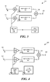
FIG. 4 depicts a pseudo-differential sigma-delta ADC, according to some embodiments; -
FIG. 5A depicts a buffer configured to add a dither signal to a received analog signal, according to some embodiments; -
FIG. 5B depicts a buffer configured to add a dither signal to a received analog signal, according to some embodiments; and -
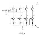
FIG. 6 depicts a digitally-controlled variable current source, according to some embodiments. - Features and advantages of the illustrated embodiments will become more apparent from the detailed description set forth below when taken in conjunction with the drawings.
- The inventors have recognized and appreciated that the performance of multi-bit sigma-delta ADCs can be improved by reducing spurious noise tones introduced by the sigma-delta modulator. The inventors have recognized and appreciated that the noise tones can be reduced by adding a filtered dither signal to two inputs of a pseudo-differential sigma-delta ADC, such that the dither output can be essentially cancelled from the ADC output signal without requiring special filtering or additional circuitry to remove the dither signal at the ADC output.
FIG. 1 depicts just one example of a sigma-delta ADC 100 in which a dither signal can be used to reduce spurious noise tones of the sigma-delta modulators. - Before describing the circuit of
FIG. 1 , it is helpful to describe three different types of circuit configurations: single-ended, fully-differential, and pseudo-differential. A single-ended circuit operates on an input signal, which may be time varying, that is referenced to another reference potential that is typically fixed or constant. In many cases, the reference potential is "ground", and conventionally represented as zero volts. A fully-differential circuit typically operates on an input signal that is carried by two wires or conductors to two input terminals of the circuit. The signal on both wires may be time varying, and the fully-differential circuit is designed to be sensitive to the difference between these two signals. However, essentially all internal signals of the circuit and also the output signal show only a little or zero sensitivity to common-mode values appearing on each input signal. - A pseudo-differential circuit also operates on an input signal that is carried by two wires or conductors to two input terminals of the circuit, where the signal on both wires may be time varying. The pseudo-differential circuit is also designed to be sensitive to the difference between these two signals, and its output signal is sensitive to the difference between these two input signals. The output signal has little or no sensitivity to the common-mode values of the two input signals. Unlike the fully-differential circuit, some or all internal signals in a pseudo-differential circuit may have considerable sensitivity to common-mode values. In some cases, a pseudo-differential circuit may consist of two independent sub-circuits, each operating on one of the two electrical input signals and each providing an output signal. Accordingly, each subcircuit will be sensitive to common-mode values appearing at each circuit's input. The two output signals may then be differenced to obtain an overall output signal from the pseudo-differential circuit. Provided that the two sub-circuits are essentially identical and linear, the overall output signal is essentially insensitive to common-mode values of the two input signals.
- The
ADC 100 ofFIG. 1 depicts a pseudo-differential circuit in which two signals output from two sigma-delta (∑Δ)converters 120 are differenced to provide an overall digital output. According to some embodiments, apseudo-differential ADC 100 comprises two analogsignal input terminals delta ADC 120 connected to receive a signal from a corresponding input terminal. Apseudo-differential ADC 100 may further comprise adigital differencing element 130 and an output terminal coupled to outputs of the ∑Δconverters 120. According to some implementations, apseudo-differential ADC 100 may further comprise a high-pass filter 115 configured to filter a received dither signal that is applied to the ∑Δ converters. Apseudo-differential ADC 100 may, or may not, include adither signal generator 110. In some cases, a dither signal may be received at a dithersignal input terminal 105. In some embodiments, thepseudo-differential ADC 100 may be connected to two output terminals of a radio-frequency antenna 101 upstream. There may be an analog low-noise amplifier between theantenna 101 andADC 100. - In operation, time varying signals may be received at
input terminals delta ADCs 120. The ∑Δ ADCs may receive a clocking signal to sample the input signals at a frequency fs , and convert each sampled signal to a digital output signal. The ADCs may also receive a filtered dither signal fromdither generator 110. The dither signal may be high-pass filtered withfilter 115, so as to attenuate "in-band" frequency components that lie within the conversion band of the ∑ΔADCs 120. According to some embodiments, the conversion band of the ADCs covers a range of frequencies from DC up to about one-half the sampling frequency fs . The same filtered dither signal may be applied to both of the ∑Δ ADCs in a manner to vary the output signals from the ∑Δ ADCs by a small amount, e.g., between 2% and 10% of their nominal output value. The digital outputs from each ∑ΔADC 120 may then be differenced (e.g., digitally subtracted) by differencingelement 130, and the resulting difference provided as a converted digital output signal representative of a difference between the two analog input signals. By taking the difference of the output signals, the dither component is removed. - The dither signal applied to the sigma-delta ADCs may be a random signal (e.g., a signal derived from white noise), or a pseudo-random signal (e.g., a signal generated by a pseudo-random signal generator). In some implementations, the dither signal may comprise a swept frequency signal or a ramp signal. When applied directly to the ∑Δ ADCs, the dither signal may add to the analog signals before conversion, or add to integration values in modulator loops of the ∑Δ converters 120 (e.g., inject charge into an integrating capacitor in each modulator loop). By adding a small dither signal to the two
converters 120, spurious noise tones associated with limit-cycle periodicity in the ∑Δ converters can be suppressed. As long as the same amount of dither is applied to each ∑Δ ADC circuit path and the twoADCs 120 respond in essentially the same way, subtraction of the signals by differencingelement 130 will effectively remove the dither signal from the overall digital output signal, so that special filtering is not needed to remove the dither signals. - The inventors have recognized and appreciated that there are second-order effects that may cause incomplete cancellation of the dither signal from the digital output of the
pseudo-differential ADC 100. For example, nonlinear intermodulation products can occur between an input signal and an applied dither signal in each circuit path. These intermodulation products can affect the digital signal value at the output of each ∑Δconverter 120. Because the intermodulation products are created by a nonlinear process, their amplitudes may not be the same for eachconverter 120. Therefore, their contributions to the outputs from theconverters 120 may not cancel each other completely after subtraction by differencingelement 130. Further, if the conversion gains of the two ∑Δconverters 120 are not exactly identical, their responses to the dither signal will differ slightly. As a result, the effects of dither may not cancel completely after subtraction. - To reduce residual dither signal components resulting from second-order effects, the inventors have recognized and appreciated that the dither signal can be filtered before being applied to each differential circuit path of the
pseudo-differential ADC 100. In some embodiments, afilter 115 is configured as a high-pass filter that attenuates in-band frequencies of the applied dither signal between approximately 3 dB and 10 dB. A small amount of attenuation of in-band frequency components of the dither signal can appreciably reduce in-band intermodulation products, because the intermodulation products are produced by a nonlinear process. For example, attenuation of in-band frequency components of the dither signal by a factor of two can reduce corresponding intermodulation products by a factor of eight. - In further detail and referring again to
FIG. 1 , each sigma-delta converter 120 may comprise analog and digital components integrated onto a semiconductor substrate. The two ∑Δconverters 120 may have a same structure, and may respond to an input signal in a same way (e.g., produce an output signal of essentially the same magnitude for a same input signal). One example of amodulator 200 for a first-order ∑Δ converter is depicted inFIG. 2 . The illustrated example is for instructional purposes only, and is not intended to limit the structure of sigma-delta converters 120. Themodulator 200 comprises the front end of a sigma-delta converter. It receives an analog signal at itsinput 201, and outputs a stream of pulses at itsoutput 250. The first-order modulator loop comprises a summingnode 210, andintegrator 220, acomparator 230, and a 1-bit digital-to-analog converter (DAC) 240. The output is fed back through theDAC 240 and is subtracted from the input signal at summingnode 210. The pulse stream from theoutput 250 may be sent to a counter (not shown), which counts the number of pulses during a sampling time interval to determine a digital signal level that corresponds to the sampled analog signal. Other types of sigma-delta converters 120 may include second-order and third-order sigma-delta converters. In some embodiments, theADCs 120 may be voltage-controlled-oscillator-based ADC. In some cases, the outputs from theADCs 120 may be single-ended outputs. Such converters may be used in apseudo-differential ADC 100, and may have additional circuit components beyond what is shown inFIG. 2 , as will be appreciated by one skilled in the art of analog-to-digital conversion. - The
filter 115 may comprise an integrated, analog high-pass filter. Any suitable filter design may be used that attenuates in-band frequency components of a received signal relative to out-of-band frequency components.Filter 115 may comprise a combination of resistive and capacitive components, in some cases, and may be integrated onto a same substrate as the sigma-delta converters 120. In some embodiments,filter 115 may be a passive filter, while in other embodiments,filter 115 may be an active filter and comprise one or more transistors. -
Differencing component 130 may comprise an integrated digital circuit configured to subtract a first received value from a second received value. For example,differencing component 130 may comprise a logic adder or an arithmetic logic unit (ALU) integrated onto a same substrate as the ∑Δconverters 120. -
Dither generator 110 may comprise any suitable random or pseudo-random signal generator. In some embodiments, dither generator may provide amplified white noise as a dither signal. In some cases, dither generator may comprise a ramp or triangular wave generator or variable frequency source. A frequency of the dither signal may be varied deterministically, pseudo-randomly, or randomly in time. Circuitry for thedither generator 110 may be integrated on a same substrate as the ∑Δconverters 120, in some cases. In some embodiments, circuitry for dither generation may be located off-chip, and theADC 100 may receive a dither signal at adither input terminal 105. - Another embodiment of a pseudo-differential sigma-
delta ADC 300 is depicted inFIG. 3 . In this embodiment, a filtered dither signal may be added to input analog signals at summingcircuits 310 in each of the two differential circuit paths. Other circuit components may be the same as described above in connection withFIG. 1 . The summingcircuits 310 may each comprise an analog summing amplifiers, according to some embodiments. -
FIG. 4 depicts a pseudo-differential sigma-delta ADC 400 that is configured to receive a pseudo-random bit sequence (PRBS) for dithering analog input signals. The ADC may compriseinput buffers 410 in each differential analog input path and a digital filter 415 configured to filter a received PRBS. The PRBS may be generated by an on-chip PRBS generator 420, or by a PRBS generator or processor located off-chip. APRBS generator 420 is configured to provide a sequence of N-bit words (N > 1) having pseudo-randomized or randomized values. The PRBS generator and digital filter may be clocked at a clock frequency fclk . According to some embodiments, the clock frequency fclk is less than one-half the ADC sampling frequency fs . - According to some embodiments, digital filter 415 is configured to attenuate in-band frequency components of the PRBS dither signal relative to out-of-band frequency components. In some embodiments, digital filter 415 comprises a finite-impulse-response (FIR) high-pass filter, though other filter designs may be used in some cases. In some implementations, digital filter 415 has a transfer function H(z) with two zeros at DC: H(z) = (1 - z-1)2. Filtered digital values may then be provided to input buffers 410.
- The input buffers may be configured to dither a received analog signal value by a small amount based upon digital values received from the digital filter 415. Subtraction at
differencing element 130 essentially removes the dither signal from the overall output digital signal. One example of aninput buffer 410 is depicted inFIG. 5A . In some implementations, the input buffer may be configured as a modified source follower. According to some embodiments, aninput buffer 410 comprises a transistor M1 connected in series with a fixedcurrent source 510 between a voltage supply Vdd and a voltage reference Vref. The voltage reference may be ground, in some implementations. The transistor M1 may be any type of transistor, e.g., a bipolar junction transistor, a junction field effect transistor, a metal-oxide-semiconductor field effect transistor, a fin field effect transistor, etc. and may be of either type (e.g., p-type or n-type). Acontrol terminal 502 of the transistor may be connected to input terminal 102 and receive an analog input signal. Anoutput terminal 525 of thebuffer 410 may connect to a node between the transistor M1 and fixedcurrent source 510. Theinput buffer 410 may further include a variablecurrent source 520 connected in parallel with the fixedcurrent source 510 between theoutput terminal 525 and reference potential Vref. The variablecurrent source 520 may be configured to receive an N-bit digital word that determines an amount of current provided by the variable current source. - For the
input buffer 410 depicted inFIG. 5A , an amount of dither current Id provided by the variablecurrent source 520 can be denoted as:
output terminal 525 is approximately equal to:
component 130, the dither signal itself need not be a precision signal. Accordingly, the variablecurrent source 520 can be constructed from simple analog circuit components (e.g., CMOS transistors and resistors). -
FIG. 5B illustrates another embodiment of aninput buffer 410 configured to dither differential analog input signals of apseudo-differential ADC 400. In some embodiments, aninput buffer 410 may further include anamplifier 530 configured to have a gain A connected to provide feedback from theoutput terminal 525 to an inverting input of the amplifier. An analog signal may be applied to thenon-inverting input terminal 502. With theamplifier 530 and feedback configuration ofFIG. 5B , the amount of dither signal ΔV can be tuned. For this circuit configuration, the amount of dither signal ΔV added tooutput terminal 525 is approximately equal to:
amplifier 530 may comprise an operational amplifier. - An example of a digitally-controlled variable
current source 520 is depicted inFIG. 6 , according to some embodiments. A variable current source may comprise a plurality of switching transistors M2, each connected in series with a fixed current source. Each fixed current source may comprise a transistor M3 connected in series with a resistor. The value of the resistor Rn may vary for each fixed current source. For example, the value of each resistor may be selected so that the current flowing in each fixed current source is given by id/2m where m=0, 1, 2, 3,... According to this circuit, a digital word received at adigital input 610 will selectively activate transistors M2 to provide a total current that is proportional to the value of the received digital word. Other embodiments of digitally controlled current sources may be used in some embodiments of input buffers 410. - The terms "approximately" and "about" may be used to mean within ±20% of a target dimension in some embodiments, within ±10% of a target dimension in some embodiments, within ±5% of a target dimension in some embodiments, and yet within ±2% of a target dimension in some embodiments. The terms "approximately" and "about" may include the target dimension.
- The technology described herein may be embodied as a method, of which at least some acts have been described. The acts performed as part of the method may be ordered in any suitable way. Accordingly, embodiments may be constructed in which acts are performed in an order different than described, which may include performing some acts simultaneously, even though described as sequential acts in illustrative embodiments. Additionally, a method may include more acts than those described, in some embodiments, and fewer acts than those described in other embodiments.
Claims (15)
- A differential analog-to-digital converter (ADC) comprising:a differential analog input comprising a first signal input terminal and a second signal input terminal;a first ADC connected to the first signal input terminal in a first signal path; anda second ADC connected to the second signal input terminal in a second signal path characterized in that the differential ADC further includes:a dither input terminal configured to receive a dither signal;a filter configured to filter the dither signal, wherein an output from the filter is coupled to both the first and second signal paths so that the output from the filter dithers output signals from the first ADC and second ADC; anda differencing circuit element that is configured to receive a first output signal from the first ADC and a second output signal from the second ADC and output a digital output signal that comprises a difference between the first output signal and the second output signal.
- The differential ADC of claim 1, wherein the first ADC has a same structure as the second ADC, such that the output signals from the first ADC and second ADC are dithered by essentially equal amounts.
- The differential ADC of claim 1 or 2, wherein the first ADC is configured to respond to an input signal to produce a first output signal of approximately the same magnitude as a second output signal produced by the second ADC in response to the input signal.
- The differential ADC of any one of claims 1 through 3, wherein the first ADC and the second ADC comprise sigma-delta modulators, or wherein the first ADC and the second ADC are voltage-controlled-oscillator-based ADCs.
- The differential ADC of any one of claims 1 through 4, wherein outputs from the first ADC and the second ADC are each single-ended outputs.
- The differential ADC of any one of claims 1 through 5, wherein the first signal path is configured to couple to a first side of a receiving antenna and the second signal path is configured to couple to a second side of the receiving antenna.
- The differential ADC of any one of claims 1 through 6, wherein the filter is a high-pass filter configured to attenuate frequency components of the dither signal in a conversion band of the first ADC and second ADC, or wherein the filter is a digital finite-impulse-response high-pass filter configured to attenuate frequency components of the dither signal in a conversion band of the first ADC and second ADC, and optionally wherein the differential ADC is a pseudo-differential circuit.
- The differential ADC of any one of claims 1 through 7, further comprising:a first analog summing circuit in the first signal path configured to add the dither signal to an analog signal from the first signal input terminal; anda second analog summing circuit in the second signal path configured to add the dither signal to an analog signal from the second signal input terminal.
- The differential ADC of any one of claims 1 through 7, further comprising:a first buffer in the first signal path configured to receive a digital dither signal and to receive an analog signal from the first signal input terminal; anda second buffer in the second signal path configured to receive the digital dither signal and to receive an analog signal from the second signal input terminal.
- The differential ADC of claim 9, wherein each buffer comprises:a source follower circuit having a transistor connected in series with a first fixed current source; anda variable current source connected in parallel with the fixed current source,
wherein the variable current source is controllable with a digital word input. - The differential ADC of claim 9, wherein each buffer comprises:a source follower circuit having a transistor connected in series with a first fixed current source;an amplifier having an output connected to a control terminal of the transistor, a non-inverting input connected to one of the first and second signal input terminals, and an inverting input connected to a node between the transistor and fixed current source; anda variable current source connected in parallel with the fixed current source,
wherein the variable current source is controllable with a digital word input. - A method for converting analog to digital signals, the method comprising:receiving, at a first input terminal, a first analog signal; andreceiving, at a second input terminal, a second analog signal characterized in that the method further includes applying essentially a same amount of dither to the first analog signal and the second analog signal to produce a first dithered analog signal and second dithered analog signal;applying the first dithered analog signal to a first ADC;applying the second dithered analog signal to a second ADC; anddifferencing output signals from the first ADC and the second ADC.
- The method of claim 12, further comprising filtering a dither signal that is applied to dither the first analog signal and second analog signal, wherein the filtering comprises high-pass filtering to attenuate frequency components of the dither signal that are in conversion bands of the first ADC and second ADC, and optionally wherein filtering the dither signal comprises filtering with a digital finite-impulse-response filter.
- The method of claim 12 or 13, wherein applying essentially a same amount of dither comprises summing a same dither signal to the first analog signal and the second analog signal.
- The method of claim 12 or 13, wherein applying essentially a same amount of dither comprises:receiving the first analog signal at a first buffer;receiving digital words at the first buffer;modulating the first analog signal at the first buffer based on the digital words;receiving the second analog signal at a second buffer;receiving the same digital words at the second buffer; andmodulating the second analog signal at the second buffer based on the digital words.
Applications Claiming Priority (3)
| Application Number | Priority Date | Filing Date | Title |
|---|---|---|---|
| US201562103182P | 2015-01-14 | 2015-01-14 | |
| US201562162245P | 2015-05-15 | 2015-05-15 | |
| US14/842,353 US9385745B1 (en) | 2015-01-14 | 2015-09-01 | Sigma-delta ADC with dither |
Publications (1)
| Publication Number | Publication Date |
|---|---|
| EP3048731A1 true EP3048731A1 (en) | 2016-07-27 |
Family
ID=55085601
Family Applications (1)
| Application Number | Title | Priority Date | Filing Date |
|---|---|---|---|
| EP16150944.3A Ceased EP3048731A1 (en) | 2015-01-14 | 2016-01-12 | Sigma-delta adc with dither |
Country Status (3)
| Country | Link |
|---|---|
| US (1) | US9385745B1 (en) |
| EP (1) | EP3048731A1 (en) |
| CN (1) | CN105790765A (en) |
Families Citing this family (10)
| Publication number | Priority date | Publication date | Assignee | Title |
|---|---|---|---|---|
| DE102016103995B4 (en) * | 2016-03-04 | 2018-03-01 | Infineon Technologies Ag | Spectrally shaped random signal |
| DE102017124818B4 (en) * | 2017-10-24 | 2022-12-22 | Infineon Technologies Ag | Method and device for signal conversion |
| US11121718B1 (en) | 2020-08-12 | 2021-09-14 | Analog Devices International Unlimited Company | Multi-stage sigma-delta analog-to-digital converter with dither |
| CN112055295B (en) * | 2020-08-24 | 2021-11-09 | 清华大学 | Method and system for driving thermoacoustic device by using digitized real-time audio signal |
| US11444635B2 (en) * | 2020-10-02 | 2022-09-13 | Texas Instruments Incorporated | Delta sigma modulator |
| CN112581971B (en) * | 2020-12-11 | 2024-05-03 | 杭州海康威视数字技术股份有限公司 | Audio signal processing method and device |
| CN113884862B (en) * | 2021-12-03 | 2022-02-22 | 北京壁仞科技开发有限公司 | Chip and chip test method |
| CN114915291A (en) * | 2022-04-26 | 2022-08-16 | 珠海市运泰利自动化设备有限公司 | Method for improving performance of test system |
| US12224761B2 (en) * | 2022-04-26 | 2025-02-11 | Texas Instruments Incorporated | Noise-shaping of additive dither in analog-to-digital converters |
| CN117879599A (en) * | 2023-12-05 | 2024-04-12 | 上海先楫半导体科技有限公司 | Signal processing device, method and system |
Citations (4)
| Publication number | Priority date | Publication date | Assignee | Title |
|---|---|---|---|---|
| US5148163A (en) * | 1990-11-15 | 1992-09-15 | Sony Corporation | Digital to analog conversion circuit with dither and overflow prevention |
| US6320526B1 (en) * | 1999-07-19 | 2001-11-20 | Stmicroelectronics S.R.L. | Sigma-delta analog/digital converter with adaptive dither |
| US6326911B1 (en) * | 1997-11-19 | 2001-12-04 | Texas Instruments Incorporated | Method and apparatus for dithering idle channel tones in delta-sigma analog-to-digital converters |
| US8766836B2 (en) * | 2012-02-10 | 2014-07-01 | Analog Devices, Inc. | Sigma delta modulator with dither |
Family Cites Families (3)
| Publication number | Priority date | Publication date | Assignee | Title |
|---|---|---|---|---|
| JP2010035098A (en) * | 2008-07-31 | 2010-02-12 | Sony Corp | Phase synchronization circuit, recording and reproducing device, and electronic device |
| US8542138B2 (en) | 2011-01-28 | 2013-09-24 | The Regents Of The University Of California | Ring oscillator delta sigma ADC modulator with replica path nonlinearity calibration |
| JP5779511B2 (en) * | 2012-01-20 | 2015-09-16 | ルネサスエレクトロニクス株式会社 | Semiconductor integrated circuit device |
-
2015
- 2015-09-01 US US14/842,353 patent/US9385745B1/en active Active
- 2015-11-25 CN CN201510833560.XA patent/CN105790765A/en not_active Withdrawn
-
2016
- 2016-01-12 EP EP16150944.3A patent/EP3048731A1/en not_active Ceased
Patent Citations (4)
| Publication number | Priority date | Publication date | Assignee | Title |
|---|---|---|---|---|
| US5148163A (en) * | 1990-11-15 | 1992-09-15 | Sony Corporation | Digital to analog conversion circuit with dither and overflow prevention |
| US6326911B1 (en) * | 1997-11-19 | 2001-12-04 | Texas Instruments Incorporated | Method and apparatus for dithering idle channel tones in delta-sigma analog-to-digital converters |
| US6320526B1 (en) * | 1999-07-19 | 2001-11-20 | Stmicroelectronics S.R.L. | Sigma-delta analog/digital converter with adaptive dither |
| US8766836B2 (en) * | 2012-02-10 | 2014-07-01 | Analog Devices, Inc. | Sigma delta modulator with dither |
Non-Patent Citations (4)
| Title |
|---|
| GERRY TAYLOR ET AL: "A Mostly-Digital Variable-Rate Continuous-Time Delta-Sigma Modulator ADC", IEEE JOURNAL OF SOLID-STATE CIRCUITS., vol. 45, no. 12, 1 December 2010 (2010-12-01), PISCATAWAY, NJ, USA, pages 2634 - 2646, XP055363347, ISSN: 0018-9200, DOI: 10.1109/JSSC.2010.2073193 * |
| GHOSH ABHISHEK ET AL: "A 50MHz bandwidth, 10-b ENOB, 8.2mW VCO-based ADC enabled by filtered-dithering based linearization", PROCEEDINGS OF THE IEEE 2013 CUSTOM INTEGRATED CIRCUITS CONFERENCE, IEEE, 22 September 2013 (2013-09-22), pages 1 - 4, XP032524698, DOI: 10.1109/CICC.2013.6658456 * |
| QIU LEI ET AL: "Source follower-based high-speed switched capacitor amplifier for pipelined ADCs", ELECTRONICS LETTERS, IEE STEVENAGE, GB, vol. 51, no. 1, 8 January 2015 (2015-01-08), pages 21 - 23, XP006050372, ISSN: 0013-5194, DOI: 10.1049/EL.2014.3171 * |
| WALT KESTER: "MT-001: Taking the Mystery out of the Infamous Formula, "SNR=6.02N + 1.76dB," and Why You Should Care", 10 March 2005 (2005-03-10), XP055271959, Retrieved from the Internet <URL:http://qtwork.tudelft.nl/~schouten/linkload/adc-tutorial.pdf> [retrieved on 20160511] * |
Also Published As
| Publication number | Publication date |
|---|---|
| US20160204793A1 (en) | 2016-07-14 |
| CN105790765A (en) | 2016-07-20 |
| US9385745B1 (en) | 2016-07-05 |
Similar Documents
| Publication | Publication Date | Title |
|---|---|---|
| US9385745B1 (en) | Sigma-delta ADC with dither | |
| CN106888018B (en) | Digital measurement of DAC timing mismatch error | |
| US9419642B1 (en) | Ultra low power dual quantizer architecture for oversampling delta-sigma modulator | |
| KR100367339B1 (en) | Sigma-Delta Converters with Digital Logic Cores | |
| Taylor et al. | A mostly-digital variable-rate continuous-time delta-sigma modulator ADC | |
| CN106888020B (en) | Digital measurement of DAC switch mismatch error | |
| US11329660B2 (en) | VCO-based continuous-time pipelined ADC | |
| EP2041875B1 (en) | Sigma-delta modulation with offset | |
| US10651870B2 (en) | Input path matching in pipelined continuous-time analog-to-digital converters | |
| US20160211861A1 (en) | System and method for measuring the dc-transfer characteristic of an analog-to-digital converter | |
| US9461660B2 (en) | Digitally-corrected analog-to-digital converters | |
| US7277032B2 (en) | Low-pass filter based delta-sigma modulator | |
| US6697001B1 (en) | Continuous-time sigma-delta modulator with discrete time common-mode feedback | |
| US11545996B1 (en) | Low-noise, high-accuracy single-ended input stage for continuous-time sigma delta (CTSD) analog-to-digital converter (ADC) | |
| US9793908B2 (en) | Protection circuits for tunable resistor at continuous-time ADC input | |
| US8400340B2 (en) | Achieving high dynamic range in a sigma delta analog to digital converter | |
| US11265010B2 (en) | Incremental analog-to-digital converter | |
| US8745115B2 (en) | Pixel sensor converters and associated apparatus and methods | |
| US10897232B2 (en) | Multi-level capacitive digital-to-analog converter for use in a sigma-delta modulator | |
| US9742426B2 (en) | Signal transfer function equalization in multi-stage delta-sigma analog-to-digital converters | |
| Tortosa et al. | A new high-level synthesis methodology of cascaded continuous-time $ SigmaDelta $ modulators | |
| JP2874218B2 (en) | A / D converter | |
| Gupta | Design techniques for low noise and high speed A/D converters | |
| EP3340474A1 (en) | Sigma-delta converter | |
| Rao et al. | A deterministic background calibration technique for voltage controlled oscillator based ADC |
Legal Events
| Date | Code | Title | Description |
|---|---|---|---|
| PUAI | Public reference made under article 153(3) epc to a published international application that has entered the european phase |
Free format text: ORIGINAL CODE: 0009012 |
|
| AK | Designated contracting states |
Kind code of ref document: A1 Designated state(s): AL AT BE BG CH CY CZ DE DK EE ES FI FR GB GR HR HU IE IS IT LI LT LU LV MC MK MT NL NO PL PT RO RS SE SI SK SM TR |
|
| AX | Request for extension of the european patent |
Extension state: BA ME |
|
| STAA | Information on the status of an ep patent application or granted ep patent |
Free format text: STATUS: REQUEST FOR EXAMINATION WAS MADE |
|
| 17P | Request for examination filed |
Effective date: 20170126 |
|
| RBV | Designated contracting states (corrected) |
Designated state(s): AL AT BE BG CH CY CZ DE DK EE ES FI FR GB GR HR HU IE IS IT LI LT LU LV MC MK MT NL NO PL PT RO RS SE SI SK SM TR |
|
| STAA | Information on the status of an ep patent application or granted ep patent |
Free format text: STATUS: EXAMINATION IS IN PROGRESS |
|
| 17Q | First examination report despatched |
Effective date: 20180702 |
|
| STAA | Information on the status of an ep patent application or granted ep patent |
Free format text: STATUS: THE APPLICATION HAS BEEN REFUSED |
|
| 18R | Application refused |
Effective date: 20191103 |