EP3048679A1 - Self-heating mitigation in an acoustic distributed feedback laser - Google Patents
Self-heating mitigation in an acoustic distributed feedback laser Download PDFInfo
- Publication number
- EP3048679A1 EP3048679A1 EP15290046.0A EP15290046A EP3048679A1 EP 3048679 A1 EP3048679 A1 EP 3048679A1 EP 15290046 A EP15290046 A EP 15290046A EP 3048679 A1 EP3048679 A1 EP 3048679A1
- Authority
- EP
- European Patent Office
- Prior art keywords
- signal
- semiconductor region
- active semiconductor
- emission wavelength
- laser
- Prior art date
- Legal status (The legal status is an assumption and is not a legal conclusion. Google has not performed a legal analysis and makes no representation as to the accuracy of the status listed.)
- Granted
Links
- 238000010438 heat treatment Methods 0.000 title claims abstract description 37
- 230000000116 mitigating effect Effects 0.000 title abstract description 9
- 239000004065 semiconductor Substances 0.000 claims abstract description 142
- 230000000737 periodic effect Effects 0.000 claims abstract description 62
- 230000003287 optical effect Effects 0.000 claims abstract description 37
- 238000010897 surface acoustic wave method Methods 0.000 claims abstract description 34
- 238000000034 method Methods 0.000 claims abstract description 28
- 230000008859 change Effects 0.000 claims abstract description 9
- 230000004044 response Effects 0.000 claims abstract description 6
- 238000007493 shaping process Methods 0.000 claims description 27
- 230000036962 time dependent Effects 0.000 claims description 23
- 230000005540 biological transmission Effects 0.000 claims description 18
- 238000012935 Averaging Methods 0.000 claims description 8
- 230000011664 signaling Effects 0.000 claims description 2
- 239000000463 material Substances 0.000 description 13
- 238000010586 diagram Methods 0.000 description 6
- 230000000712 assembly Effects 0.000 description 5
- 238000000429 assembly Methods 0.000 description 5
- 230000000694 effects Effects 0.000 description 5
- 230000003993 interaction Effects 0.000 description 3
- 230000008901 benefit Effects 0.000 description 2
- 230000015556 catabolic process Effects 0.000 description 1
- 230000003247 decreasing effect Effects 0.000 description 1
- 238000006731 degradation reaction Methods 0.000 description 1
- 230000001934 delay Effects 0.000 description 1
- 238000009533 lab test Methods 0.000 description 1
- 230000007246 mechanism Effects 0.000 description 1
- 230000004048 modification Effects 0.000 description 1
- 238000012986 modification Methods 0.000 description 1
- 238000012545 processing Methods 0.000 description 1
- 239000000758 substrate Substances 0.000 description 1
Images


Classifications
-
- H—ELECTRICITY
- H01—ELECTRIC ELEMENTS
- H01S—DEVICES USING THE PROCESS OF LIGHT AMPLIFICATION BY STIMULATED EMISSION OF RADIATION [LASER] TO AMPLIFY OR GENERATE LIGHT; DEVICES USING STIMULATED EMISSION OF ELECTROMAGNETIC RADIATION IN WAVE RANGES OTHER THAN OPTICAL
- H01S5/00—Semiconductor lasers
- H01S5/10—Construction or shape of the optical resonator, e.g. extended or external cavity, coupled cavities, bent-guide, varying width, thickness or composition of the active region
- H01S5/12—Construction or shape of the optical resonator, e.g. extended or external cavity, coupled cavities, bent-guide, varying width, thickness or composition of the active region the resonator having a periodic structure, e.g. in distributed feedback [DFB] lasers
- H01S5/1234—Actively induced grating, e.g. acoustically or electrically induced
-
- H—ELECTRICITY
- H01—ELECTRIC ELEMENTS
- H01S—DEVICES USING THE PROCESS OF LIGHT AMPLIFICATION BY STIMULATED EMISSION OF RADIATION [LASER] TO AMPLIFY OR GENERATE LIGHT; DEVICES USING STIMULATED EMISSION OF ELECTROMAGNETIC RADIATION IN WAVE RANGES OTHER THAN OPTICAL
- H01S5/00—Semiconductor lasers
- H01S5/06—Arrangements for controlling the laser output parameters, e.g. by operating on the active medium
- H01S5/0617—Arrangements for controlling the laser output parameters, e.g. by operating on the active medium using memorised or pre-programmed laser characteristics
-
- H—ELECTRICITY
- H01—ELECTRIC ELEMENTS
- H01S—DEVICES USING THE PROCESS OF LIGHT AMPLIFICATION BY STIMULATED EMISSION OF RADIATION [LASER] TO AMPLIFY OR GENERATE LIGHT; DEVICES USING STIMULATED EMISSION OF ELECTROMAGNETIC RADIATION IN WAVE RANGES OTHER THAN OPTICAL
- H01S5/00—Semiconductor lasers
- H01S5/06—Arrangements for controlling the laser output parameters, e.g. by operating on the active medium
- H01S5/068—Stabilisation of laser output parameters
Definitions
- This application relates to laser assemblies (laser modules) comprising semiconductor lasers, particularly for use in burst-mode operation, and to methods for driving semiconductor lasers, particularly in burst-mode operation.
- the application particularly relates to laser modules comprising acoustically tunable distributed feedback (ADFB) lasers and methods for driving ADFB lasers in burst-mode operation.
- ADFB distributed feedback
- Directly tunable lasers such as e.g. distributed feedback (DFB) lasers suffer from self-heating induced wavelength drifts during burst-mode operation. In signal processing, this drift results in signal degradations when signals generated by these lasers are passed through narrowband wavelength filters at the receive side, e.g. at the optical line termination (OLT) in a time and wavelength division multiplexed passive optical network (TWDM-PON).
- OLT optical line termination
- TWDM-PON time and wavelength division multiplexed passive optical network
- ADFB lasers A number of generic mitigation techniques that are applicable to ADFB lasers have been proposed so far, e.g. applying accelerated heating, elevated subthreshold bias current or operation at low output powers.
- these mitigation techniques in order for these mitigation techniques to be efficient, the respective ADFB laser would need to be driven in a non-optimal point of operation, resulting in system penalties due to e.g. lower power or degraded eye openings.
- the present document proposes a laser assembly and a method of driving a semiconductor laser having the features of the respective independent claims.
- the laser assembly may comprise a semiconductor laser with an (optically) active region or gain region (an active semiconductor region) for emitting an optical signal in response to a drive current that is applied to the active semiconductor region, i.e. that is injected to the active semiconductor region, and a drive circuit for generating the drive current in accordance with an input signal and applying the drive current to the active semiconductor region.
- the laser assembly may further comprise a controllable oscillator for generating a periodic electric signal that is used to generate a surface acoustic wave (SAW) in the semiconductor laser.
- SAW surface acoustic wave
- the periodic electric signal may be applied to layers or regions of the semiconductor laser that comprise piezoelectric electrodes and are arranged in proximity to the active semiconductor region.
- the surface acoustic wave may be a standing wave.
- the surface acoustic wave may be generated such that a laser mode in the active semiconductor region may interact with the surface acoustic wave. This interaction may take place in or near the active semiconductor region.
- a diffraction grating structure i.e. a periodic modulation of the diffraction index of the semiconductor material
- the semiconductor laser e.g. in or near the active semiconductor region
- An emission wavelength of the active semiconductor region may be determined (set) by a periodicity of the diffraction grating structure (i.e. by a lattice constant of the diffraction grating structure), or correspondingly, by a wavelength of the surface acoustic wave.
- the controllable oscillator may be configured to set a frequency of the periodic electric signal in accordance with a control signal.
- the laser assembly may further comprise a control circuit for generating the control signal for the controllable oscillator.
- the control circuit may generate the control signal in such a manner that a shift of the emission wavelength away from a predetermined emission wavelength, the shift resulting from heating of the active semiconductor region during emission of the optical signal, is at least partially compensated by an opposite shift of the emission wavelength that results from a change of the periodicity of the diffraction grating structure in or near the active semiconductor region.
- control signal may be configured such that the controllable oscillator is controlled to change the frequency of the periodic electric signal away from a predetermined frequency corresponding to a periodicity of the diffraction grating structure that would, in the absence of self-heating, result in emission at the predetermined emission wavelength.
- the semiconductor laser may be operated in burst-mode to emit the optical signal during respective transmission periods and to not emit the optical signal in the intervals between successive transmission periods.
- the laser assembly is enabled to keep constant the emission wavelength of the semiconductor laser in a simple and efficient, and non-signal-degrading manner. This is achieved by taking advantage of the working principle of the ADFB laser, for which the emission wavelength is set by a wavelength of a standing surface acoustic wave inside the semiconductor material.
- the self-heating mitigation technique employed by the laser assembly does not require modification of the semiconductor laser as such, but merely requires generation of a modified control signal for the controllable oscillator responsible for generating the surface acoustic wave. Consequently, costs for implementing the mitigation technique at hand are very low.
- the self-heating induced drift of the emission wavelength can be substantially cancelled, which makes the laser assembly a perfect candidate for use e.g. in TWDM-PONs with filter widths of 50 GHz or less, such as a NG-PON2 network.
- control signal may be a time-dependent control signal.
- the control circuit may be configured to generate the control signal in such a manner that the controllable oscillator is controlled to increase the frequency of the periodic electric signal during emission of the optical signal, i.e. during respective transmission periods in burst mode operation.
- the wavelength of the standing surface acoustic wave in the semiconductor material needs to be reduced in order to compensate the self-heating induced shift of the emission wavelength. This is achieved by controlling the controllable oscillator to increase the frequency of the periodic electric signal that is applied to the semiconductor laser during periods of time where the semiconductor laser is operating and the optical signal is emitted.
- control signal may comprise a constant contribution corresponding to the predetermined emission wavelength of the optical signal and a time-dependent contribution corresponding to the shift of the emission wavelength opposite to the shift due to self-heating.
- Tuning the constant contribution to the control signal allows to adapt the laser assembly to different desired emission wavelengths, whereas the time-dependent contribution allows to compensate for a self-heating induced shift of the emission wavelength during data bursts of the laser assembly.
- control circuit may be configured to generate the control signal on the basis of the input signal that is also used by the drive circuit for deriving the drive current for the active semiconductor region.
- control circuit receives a copy of the input signal to generate the control signal based thereupon.
- the input signal may comprise a rectangular pulse (a burst enable signal; e.g. as a rectangular pulse of a sequence of rectangular pulses, each rectangular pulse corresponding to a respective transmission period) indicating the transmission period
- the control signal may be generated on the basis of the rectangular pulse.
- the control signal may be generated on the basis of a shape of the rectangular pulse, in particular the time instants of pulse edges i.e. when the pulse begins and ends, and the height of the pulse.
- the control signal may correspond to its constant contribution unless the rectangular pulse is present.
- the control circuit may comprise a pulse shaping circuit for generating an output voltage level (a voltage signal) depending on the rectangular pulse, and the controllable oscillator may be a voltage controlled oscillator (VCO).
- VCO voltage controlled oscillator
- the input signal may comprise a data signal indicative of data to be transmitted by means of the optical signal.
- the control circuit may be configured to determine an envelope of the data signal, and the control signal may be generated on the basis of the envelope of the data signal. In particular, the control signal may be generated on the basis of a shape of the envelope of the data signal.
- the control circuit may comprise an averaging circuit for determining the envelope of the data signal and a pulse shaping circuit for generating an output voltage level (a voltage signal) depending on the determined envelope of the data signal.
- the averaging circuit may be a low pass filter.
- the controllable oscillator may be a voltage controlled oscillator.
- burst enable signal or to (the envelope of) the data signal provides for convenient means of deriving the control signal necessary for compensating the self-heating induced drift of the emission wavelength during data bursts.
- the pulse shaping circuit may comprise a look-up table or a filter unit which may be implemented as an analog electrical filter, or a digital filter.
- a look-up table or a filter unit which may be implemented as an analog electrical filter, or a digital filter.
- an analog-to-digital converter and a digital to analog converter may be provided in the pulse shaping circuit.
- the look-up table may be configured to relate a pulse shape input to the pulse shaping circuit to an appropriate time-dependent voltage level (voltage signal) resulting in a time-dependent frequency of the periodic electric signal that in turn results in a periodicity of the diffraction grating structure that compensates for the drift of the emission wavelength due to self-heating effects.
- the filter unit may be configured to output, for a pulse shape input to the, pulse shaping circuit, an appropriate time-dependent signal (e.g. a voltage signal) resulting in a time-dependent frequency of the periodic electric signal that in turn results in a periodicity of the diffraction grating structure that compensates for the drift of the emission wavelength due to self-heating effects.
- the pulse-shaping circuit may also apply a self-learning algorithm to determine appropriate time-dependent output voltage levels on the basis of input pulse shapes.
- the pulse shaping circuit may comprise a delay element that delays output of the time-dependent voltage level (voltage signal).
- the semiconductor laser may have an (optically) active region or gain region (an active semiconductor region) for emitting an optical signal in response to a drive current that is applied to the active semiconductor region, i.e. that is injected to the active semiconductor region.
- the method may comprise generating the drive current in accordance with an input signal and applying the drive current to the active semiconductor region.
- the method may further comprise generating a surface acoustic wave in the active semiconductor region by using a periodic electric signal.
- the method may comprise applying the periodic electric signal to the semiconductor laser, such that a diffraction grating structure (i.e. a periodic modulation of the diffraction index of the semiconductor material) is created in the semiconductor laser (e.g.
- the periodic electric signal may be applied to layers or regions of the semiconductor laser that comprise piezoelectric electrodes and are arranged in proximity to the active semiconductor region.
- the surface acoustic wave may be a standing wave.
- the surface acoustic wave may be generated such that a laser mode in the active semiconductor region may interact with the diffraction grating structure generated by the surface acoustic wave. This interaction may take place in or near the active semiconductor region.
- An emission wavelength of the active semiconductor region may be determined (set) by a periodicity of the diffraction grating structure (i.e. by a lattice constant of the diffraction grating structure), or correspondingly, by a wavelength of the surface acoustic wave.
- the method may further comprise controlling a frequency of the periodic electric signal in such a manner that a shift of the emission wavelength away from a predetermined emission wavelength, the shift resulting from heating of the active semiconductor region during emission of the optical signal, is at least partially compensated by an opposite shift of the emission wavelength that results from a change of the periodicity of the diffraction grating structure in the active semiconductor region.
- the frequency of the periodic electric signal may be controlled to change away from a predetermined frequency corresponding to a periodicity of the diffraction grating structure that would, in the absence of self-heating, result in emission at the predetermined emission wavelength, in order to compensate self-heating effects on emission wavelength.
- the semiconductor laser may be operated in burst-mode to emit the optical signal during respective transmission periods and to not emit the optical signal in the intervals between successive transmission periods. The above described compensation is applied during transmission periods where the laser is in operation and generates heat that may produce wavelength drifts.
- controlling the frequency of the electric signal may involve increasing the frequency of the periodic electric signal during emission of the optical signal, i.e. during respective transmission periods.
- controlling the frequency of the electric signal may involve controlling the frequency of the periodic electric signal on the basis of the input signal that is also used for deriving the drive current for the active semiconductor region.
- the input signal may comprise a rectangular pulse (a burst enable signal; e.g. as a rectangular pulse of a sequence of rectangular pulses, each rectangular pulse corresponding to a respective transmission period) indicating a transmission period.
- Controlling the frequency of the periodic electric signal may involve controlling the frequency of the periodic electric signal on the basis of the rectangular pulse. In particular, this may involve controlling the frequency of the periodic electric signal on the basis of a shape of the rectangular pulse.
- the input signal may comprise a data signal indicative of data to be transmitted by means of the optical signal.
- Controlling the frequency of the periodic electric signal may involve determining an envelope of the data signal and controlling the frequency of the periodic electric signal on the basis of the envelope of the data signal. In particular, this may involve controlling the frequency of the periodic electric signal on the basis of a shape of the envelope of the data signal.
- Fig. 1 schematically illustrates an example of a laser assembly (laser module) 100 according to embodiments of the disclosure.
- the laser assembly 100 comprises a semiconductor laser 110, which is an ADFB laser or any other semiconductor laser in which a diffraction grating structure is created by means of generating a surface acoustic wave in the semiconductor material, and a drive circuit (laser driver) 120 for driving the semiconductor laser 110, i.e. for generating a drive current for the semiconductor laser 110.
- the laser assembly 100 receives an input signal from a logic circuit (e.g. a PON logic) 130 and feeds the input signal to the drive circuit 120.
- the laser assembly 100 further comprises a controllable oscillator (oscillator circuit, e.g.
- the laser assembly 100 further comprises a pulse shaping circuit (pulse shaper) 160.
- pulse shaper pulse shaper
- the semiconductor laser 110 comprises an active semiconductor region (gain region, optically active region) for emitting an optical signal in response to the drive current that is applied to the active semiconductor region.
- the active semiconductor region may be a semiconductor layer or part of a semiconductor layer.
- the wavelength selection mechanism of the semiconductor laser 110 (which may be an ADFB laser) is based on creating a standing surface acoustic wave inside the semiconductor material. Presence of the standing surface' acoustic wave in the semiconductor material results in a periodic modulation of the diffraction index of the semiconductor material (e.g. in or near the active semiconductor region), and thus effectively generates a diffraction grating structure.
- the wavelength of the surface acoustic wave in the semiconductor material i.e.
- the periodicity (lattice constant) of the diffraction grating structure determines the wavelength of the optical emission of the semiconductor laser 110 by interaction, in or near the active semiconductor region, of the laser mode in the active semiconductor region with the diffraction grating structure.
- the controllable oscillator 140 generates a periodic electric signal (an RF driving signal) that is applied to the semiconductor laser 110.
- the periodic electric signal may be applied to layers or regions of the semiconductor laser 110 that comprise piezoelectric electrodes and are arranged in proximity to the active semiconductor region.
- the periodic electric signal may be a periodic voltage signal.
- Application of the periodic electric signal to the semiconductor laser 110 creates the standing surface acoustic wave in the semiconductor material, i.e. also in or near the active semiconductor region, e.g. through the piezo-electric effect.
- a frequency of the periodic electric signal is set by the controllable oscillator 140 in accordance with a control signal (e.g. a voltage signal) that is input to the controllable oscillator 140.
- a control signal e.g. a voltage signal
- the emission wavelength of the semiconductor laser 110 can be tuned by changing the frequency of the periodic electric signal that is applied to the semiconductor material and that creates the surface acoustic wave.
- the controllable voltage source 150 generates a voltage signal that forms a contribution to the control signal that is input to the controllable oscillator 140.
- the voltage signal generated by the controllable voltage source 150 is constant.
- the emission wavelength of the semiconductor laser 110 can be tuned by changing the voltage level of the voltage signal generated by the controllable voltage source 150, while during operation of the semiconductor laser 110 the voltage level of the voltage signal generated by the controllable voltage source 150 remains constant, as indicated above.
- the input signal generated by the logic circuit 130 comprises a burst enable signal (a sequence of rectangular pulses, each rectangular pulse corresponding to a respective transmission period) indicating transmission periods of the semiconductor laser 110 and biasing the semiconductor laser 110 at its operation point, and a data signal indicating actual data to be transmitted by means of optical emission by the semiconductor laser 110.
- the burst enable signal and the data signal are fed to the drive circuit 120, and the burst enable signal is additionally fed to the pulse shaping circuit 160.
- the drive circuit 120 generates the drive current that is applied to the active semiconductor region of the semiconductor laser 110 on the basis of the input signal, i.e. on the basis of the burst enable signal and/or the data signal.
- the emission wavelength of the semiconductor laser 110 changes during a burst (i.e. during a transmission period) due to the self-heating effect in the active semiconductor region of the semiconductor laser 110
- this shift of emission wavelength is compensated for, at least partially, by slightly detuning the frequency of the periodic electric signal (RF driving frequency) generated by the controllable oscillator 140.
- the frequency of the periodic electric signal is slightly detuned such as to modify the wavelength of the standing surface acoustic wave (and correspondingly the periodicity of the diffraction grating structure) in the semiconductor material and thus to shift the emission wavelength of the semiconductor laser 110 into the opposite direction compared to the self-heating induced shift. If implemented correctly, the self-heating induced shift and the surface acoustic wave induced shift cancel out each other.
- the burst enable signal included in the input signal which essentially corresponds to a sequence of rectangular pulses (each rectangular pulse corresponding to a respective transmission period), is fed to the pulse shaping circuit 160, as indicated above.
- the pulse shaping circuit 160 generates a time-dependent contribution to the control signal, on the basis of the burst enable signal (e.g. on the basis of a shape thereof). For instance, the pulse shaping circuit 160 may generate a time-dependent voltage signal on the basis of the burst enable signal, i.e. output a time-dependent voltage level depending on the burst enable signal.
- the pulse shaping circuit 160 is configured to generate the time-dependent contribution to the control signal for the controllable oscillator 140 in such a manner that appropriate detuning of the frequency of the periodic electric signal (and correspondingly, an appropriate shift of the emission wavelength that cancels the self-heating induced shift) is achieved.
- the controllable voltage source 150 and the pulse shaping circuit 160 may be said to form a control circuit for generating the control signal for the controllable oscillator 140 on the basis of the input signal.
- the control circuit for generating the control signal for the controllable oscillator 140 can be said to generate the control signal in such a manner that a shift of the emission wavelength away from a predetermined emission wavelength, that results from heating of the active semiconductor region during emission of the optical signal (i.e. from self-heating), is at least partially-compensated by an opposite shift of the emission wavelength that results from the change of the periodicity of the diffraction grating structure in or near the active semiconductor region.
- Fig. 2 schematically illustrates another example of a laser assembly (laser module) 200 according to embodiments of the disclosure.
- the laser assembly 200 comprises the semiconductor laser 110, the drive circuit 120, the controllable oscillator 140, the controllable voltage source 150, and the pulse shaping circuit 160 described above with reference to Fig. 1 , and receives an input signal from the logic circuit 130 for feeding to the drive circuit 120. Unless indicated otherwise, these components of the laser assembly 200 correspond to respective like-numbered components of the laser assembly 100 described above.
- the laser assembly 200 of Fig. 2 further comprises an averaging circuit (averager) 170 to which the data signal output by the logic circuit 130 is fed.
- the averaging circuit 170 may be a low pass filter.
- the burst enable signal is not fed to the pulse shaping circuit 160 in this configuration.
- detuning the frequency of the periodic electric signal is performed as follows.
- the data signal included in the input signal is fed to the averaging circuit 170, as indicated above.
- the averaging circuit 170 generates an envelope of the data signal on the basis of the data signal.
- Said envelope of the data signal which is essentially a sequence of rectangular pulses (each rectangular pulse corresponding to a respective transmission period), is fed to the pulse shaping circuit 160.
- the pulse shaping circuit 160 generates a time-dependent contribution to the control signal on the basis of the envelope of the data signal (e.g. on the basis of a shape thereof).
- the pulse shaping circuit 160 may generate a time-dependent voltage signal (output a time dependent voltage signal) on the basis of the envelope of the data signal.
- the pulse shaping circuit 160 is configured to generate the time-dependent contribution to the control signal for the controllable oscillator 140 in such a manner that appropriate detuning of the frequency of the periodic electric signal (and correspondingly, an appropriate shift of the emission wavelength that cancels the self-heating induced shift) is achieved.
- the controllable voltage source 150, the pulse shaping circuit 160, and the averaging circuit 170 may be said to form a control circuit for generating the control signal for the controllable oscillator 140 on the basis of the input signal.
- the control circuit for generating the control signal for the controllable oscillator 140 can be said to generate the control signal in such a manner that a shift of the emission wavelength away from a predetermined emission wavelength, that results from heating of the active semiconductor region during emission of the optical signal (i.e. from self-heating), is-at least partially-compensated by an opposite shift of the emission wavelength that results from the change of the periodicity of the diffraction grating structure in or near the active semiconductor region.
- the required amount of detuning of the frequency of the periodic electric signal as well as its time-dependence have to be determined on a per laser structure and/or wafer basis, i.e. by measuring and evaluating a couple of sample devices.
- the appropriate detuning can be implemented by e.g. using one or more look-up tables in generating (the time-dependent contribution to) the control signal, or by generating (the time-dependent contribution to) the control signal using an appropriate filter unit, e.g. implemented as a digital filter or an analog electrical filter.
- the look-up table and the filter unit may be comprised by the pulse shaping circuit 160.
- control circuit may be configured to generate the control signal in such a manner that the frequency of the periodic electric signal is increased during a data burst (during emission of the optical signal), i.e. the control circuit may control the controllable oscillator 140 to increase the frequency of the periodic electric signal during the data burst.
- the control circuit may control the controllable oscillator 140 to increase the frequency of the periodic electric signal during the data burst.
- self-heating results in a gradual increase of the emission wavelength of the semiconductor laser 110.
- the wavelength of the standing surface acoustic wave i.e. the periodicity of the diffraction grating structure
- the periodic electric signal i.e. the periodicity of the diffraction grating structure
- Fig. 3 schematically illustrates an example of a semiconductor laser 110 in laser assemblies according to embodiments of the disclosure.
- the semiconductor laser 110 comprises a semiconductor substrate 310, 320 and an active semiconductor region (active region, gain region), or laser stripe 350.
- the active semiconductor region 350 borders on layers 330, 340 comprising piezoelectric electrodes that are driven by the periodic electric signal and generate the surface acoustic wave. It is understood that alternative means for generating the surface acoustic wave are readily apparent to the skilled person and that the present disclosure shall not be construed to be limited to the use of piezoelectric electrodes for generating the surface acoustic wave.
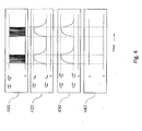
- Fig. 4 is an exemplary schematic timing diagram of time-dependent quantities related to operation of laser assemblies according to embodiments of the invention.
- the topmost diagram 410 indicates the laser drive current output by the drive circuit 120 and injected to the active semiconductor region of the semiconductor laser 110, and the output optical power of the semiconductor laser 110.
- the laser drive current and the output optical power are illustrated to have qualitatively the same variation in time.
- the second diagram 420 from the top indicates the laser temperature within the active semiconductor layer and the emission wavelength of the optical signal output by the semiconductor laser 110 during data bursts, both for a case in which the self-heating technique according to the disclosure is not applied.
- the laser temperature and the emission wavelength are schematically illustrated to have qualitatively the same variation in time.
- the emission wavelength is understood to be zero during intervals between data bursts.
- the third diagram 430 from the top indicates the control signal (voltage signal) that is input to the controllable oscillator 140 and the frequency of the periodic electric signal output by the controllable oscillator 140. Also the control signal and the frequency of the periodic electric signal are schematically illustrated to have qualitatively the same variation, in time.
- the lowermost diagram 440 indicates the emission wavelength of the optical signal output by the semiconductor laser 110 during data bursts for the case in which the self-heating technique according to the disclosure is applied.
- the laser temperature rises during data bursts, and the emission wavelength increases proportionally to the temperature increase.
- the control signal for the controllable oscillator 140 as well as the frequency of the periodic electric signal output by the controllable oscillator 140 are substantially proportional to the drift of the emission wavelength. If the self-heating mitigation technique according to the disclosure is applied, the emission wavelength is substantially constant over time during data bursts.
Landscapes
- Physics & Mathematics (AREA)
- Condensed Matter Physics & Semiconductors (AREA)
- General Physics & Mathematics (AREA)
- Electromagnetism (AREA)
- Optics & Photonics (AREA)
- Acoustics & Sound (AREA)
- Semiconductor Lasers (AREA)
Abstract
Description
- This application relates to laser assemblies (laser modules) comprising semiconductor lasers, particularly for use in burst-mode operation, and to methods for driving semiconductor lasers, particularly in burst-mode operation. The application particularly relates to laser modules comprising acoustically tunable distributed feedback (ADFB) lasers and methods for driving ADFB lasers in burst-mode operation.
- Directly tunable lasers, such as e.g. distributed feedback (DFB) lasers suffer from self-heating induced wavelength drifts during burst-mode operation. In signal processing, this drift results in signal degradations when signals generated by these lasers are passed through narrowband wavelength filters at the receive side, e.g. at the optical line termination (OLT) in a time and wavelength division multiplexed passive optical network (TWDM-PON). This issue also applies to ADFB lasers, so that conventional ADFB lasers are not useable in networks with filter widths in the order of 50 GHz or less.
- A number of generic mitigation techniques that are applicable to ADFB lasers have been proposed so far, e.g. applying accelerated heating, elevated subthreshold bias current or operation at low output powers. However, in order for these mitigation techniques to be efficient, the respective ADFB laser would need to be driven in a non-optimal point of operation, resulting in system penalties due to e.g. lower power or degraded eye openings.
- Thus, there is a need for improved self-heating mitigation techniques applicable to ADFB lasers.
- In view of this need, the present document proposes a laser assembly and a method of driving a semiconductor laser having the features of the respective independent claims.
- An aspect of the disclosure relates to a laser assembly (a laser module). The laser assembly may comprise a semiconductor laser with an (optically) active region or gain region (an active semiconductor region) for emitting an optical signal in response to a drive current that is applied to the active semiconductor region, i.e. that is injected to the active semiconductor region, and a drive circuit for generating the drive current in accordance with an input signal and applying the drive current to the active semiconductor region. The laser assembly may further comprise a controllable oscillator for generating a periodic electric signal that is used to generate a surface acoustic wave (SAW) in the semiconductor laser. By applying the periodic electric signal to the semiconductor laser, a surface acoustic wave is generated in the semiconductor material. The periodic electric signal may be applied to layers or regions of the semiconductor laser that comprise piezoelectric electrodes and are arranged in proximity to the active semiconductor region. The surface acoustic wave may be a standing wave. The surface acoustic wave may be generated such that a laser mode in the active semiconductor region may interact with the surface acoustic wave. This interaction may take place in or near the active semiconductor region. Due to the presence of the surface acoustic wave, a diffraction grating structure (i.e. a periodic modulation of the diffraction index of the semiconductor material) is created in the semiconductor laser (e.g. in or near the active semiconductor region) and may interact with the laser mode in the active semiconductor region. An emission wavelength of the active semiconductor region may be determined (set) by a periodicity of the diffraction grating structure (i.e. by a lattice constant of the diffraction grating structure), or correspondingly, by a wavelength of the surface acoustic wave.
- The controllable oscillator may be configured to set a frequency of the periodic electric signal in accordance with a control signal. The laser assembly may further comprise a control circuit for generating the control signal for the controllable oscillator. The control circuit may generate the control signal in such a manner that a shift of the emission wavelength away from a predetermined emission wavelength, the shift resulting from heating of the active semiconductor region during emission of the optical signal, is at least partially compensated by an opposite shift of the emission wavelength that results from a change of the periodicity of the diffraction grating structure in or near the active semiconductor region. To this end, the control signal may be configured such that the controllable oscillator is controlled to change the frequency of the periodic electric signal away from a predetermined frequency corresponding to a periodicity of the diffraction grating structure that would, in the absence of self-heating, result in emission at the predetermined emission wavelength. The semiconductor laser may be operated in burst-mode to emit the optical signal during respective transmission periods and to not emit the optical signal in the intervals between successive transmission periods.
- Configured as above, the laser assembly is enabled to keep constant the emission wavelength of the semiconductor laser in a simple and efficient, and non-signal-degrading manner. This is achieved by taking advantage of the working principle of the ADFB laser, for which the emission wavelength is set by a wavelength of a standing surface acoustic wave inside the semiconductor material. Notably, the self-heating mitigation technique employed by the laser assembly does not require modification of the semiconductor laser as such, but merely requires generation of a modified control signal for the controllable oscillator responsible for generating the surface acoustic wave. Consequently, costs for implementing the mitigation technique at hand are very low. By appropriately choosing the shift in frequency of the periodic electric signal, the self-heating induced drift of the emission wavelength can be substantially cancelled, which makes the laser assembly a perfect candidate for use e.g. in TWDM-PONs with filter widths of 50 GHz or less, such as a NG-PON2 network.
- In embodiments, the control signal may be a time-dependent control signal. The control circuit may be configured to generate the control signal in such a manner that the controllable oscillator is controlled to increase the frequency of the periodic electric signal during emission of the optical signal, i.e. during respective transmission periods in burst mode operation.
- Since self-heating of the semiconductor laser results in an increase of the emission wavelength of the active semiconductor region, the wavelength of the standing surface acoustic wave in the semiconductor material needs to be reduced in order to compensate the self-heating induced shift of the emission wavelength. This is achieved by controlling the controllable oscillator to increase the frequency of the periodic electric signal that is applied to the semiconductor laser during periods of time where the semiconductor laser is operating and the optical signal is emitted.
- In embodiments, the control signal may comprise a constant contribution corresponding to the predetermined emission wavelength of the optical signal and a time-dependent contribution corresponding to the shift of the emission wavelength opposite to the shift due to self-heating.
- Tuning the constant contribution to the control signal allows to adapt the laser assembly to different desired emission wavelengths, whereas the time-dependent contribution allows to compensate for a self-heating induced shift of the emission wavelength during data bursts of the laser assembly.
- In embodiments, the control circuit may be configured to generate the control signal on the basis of the input signal that is also used by the drive circuit for deriving the drive current for the active semiconductor region. Thus, the control circuit receives a copy of the input signal to generate the control signal based thereupon.
- In embodiments, the input signal may comprise a rectangular pulse (a burst enable signal; e.g. as a rectangular pulse of a sequence of rectangular pulses, each rectangular pulse corresponding to a respective transmission period) indicating the transmission period, and the control signal may be generated on the basis of the rectangular pulse. In particular, the control signal may be generated on the basis of a shape of the rectangular pulse, in particular the time instants of pulse edges i.e. when the pulse begins and ends, and the height of the pulse. The control signal may correspond to its constant contribution unless the rectangular pulse is present. Further, the control circuit may comprise a pulse shaping circuit for generating an output voltage level (a voltage signal) depending on the rectangular pulse, and the controllable oscillator may be a voltage controlled oscillator (VCO).
- In embodiments, the input signal may comprise a data signal indicative of data to be transmitted by means of the optical signal. The control circuit may be configured to determine an envelope of the data signal, and the control signal may be generated on the basis of the envelope of the data signal. In particular, the control signal may be generated on the basis of a shape of the envelope of the data signal. Further, the control circuit may comprise an averaging circuit for determining the envelope of the data signal and a pulse shaping circuit for generating an output voltage level (a voltage signal) depending on the determined envelope of the data signal. For example, the averaging circuit may be a low pass filter. The controllable oscillator may be a voltage controlled oscillator.
- Referring to the burst enable signal or to (the envelope of) the data signal provides for convenient means of deriving the control signal necessary for compensating the self-heating induced drift of the emission wavelength during data bursts.
- In embodiments, the pulse shaping circuit may comprise a look-up table or a filter unit which may be implemented as an analog electrical filter, or a digital filter. For the case of the pulse shaping circuit comprising the look-up table or the digital filter, an analog-to-digital converter and a digital to analog converter may be provided in the pulse shaping circuit. The look-up table may be configured to relate a pulse shape input to the pulse shaping circuit to an appropriate time-dependent voltage level (voltage signal) resulting in a time-dependent frequency of the periodic electric signal that in turn results in a periodicity of the diffraction grating structure that compensates for the drift of the emission wavelength due to self-heating effects. Likewise, the filter unit may be configured to output, for a pulse shape input to the, pulse shaping circuit, an appropriate time-dependent signal (e.g. a voltage signal) resulting in a time-dependent frequency of the periodic electric signal that in turn results in a periodicity of the diffraction grating structure that compensates for the drift of the emission wavelength due to self-heating effects. The pulse-shaping circuit may also apply a self-learning algorithm to determine appropriate time-dependent output voltage levels on the basis of input pulse shapes. Further, the pulse shaping circuit may comprise a delay element that delays output of the time-dependent voltage level (voltage signal).
- Employing one or more appropriately prepared look-up tables or an appropriately configured filter unit enables to derive the control signal necessary for compensating the self-heating induced drift of the emission wavelength during data bursts based on the burst enable signal or the envelope of the data signal. Any required calibration may be encapsulated in these look-up tables or filter unit such as an analog electric filter.
- Another aspect of the disclosure relates to a method of driving a semiconductor laser. The semiconductor laser may have an (optically) active region or gain region (an active semiconductor region) for emitting an optical signal in response to a drive current that is applied to the active semiconductor region, i.e. that is injected to the active semiconductor region. The method may comprise generating the drive current in accordance with an input signal and applying the drive current to the active semiconductor region. The method may further comprise generating a surface acoustic wave in the active semiconductor region by using a periodic electric signal. The method may comprise applying the periodic electric signal to the semiconductor laser, such that a diffraction grating structure (i.e. a periodic modulation of the diffraction index of the semiconductor material) is created in the semiconductor laser (e.g. in or near the active semiconductor region) by the surface acoustic wave. The periodic electric signal may be applied to layers or regions of the semiconductor laser that comprise piezoelectric electrodes and are arranged in proximity to the active semiconductor region. The surface acoustic wave may be a standing wave. The surface acoustic wave may be generated such that a laser mode in the active semiconductor region may interact with the diffraction grating structure generated by the surface acoustic wave. This interaction may take place in or near the active semiconductor region. An emission wavelength of the active semiconductor region may be determined (set) by a periodicity of the diffraction grating structure (i.e. by a lattice constant of the diffraction grating structure), or correspondingly, by a wavelength of the surface acoustic wave.
- The method may further comprise controlling a frequency of the periodic electric signal in such a manner that a shift of the emission wavelength away from a predetermined emission wavelength, the shift resulting from heating of the active semiconductor region during emission of the optical signal, is at least partially compensated by an opposite shift of the emission wavelength that results from a change of the periodicity of the diffraction grating structure in the active semiconductor region. To this end, the frequency of the periodic electric signal may be controlled to change away from a predetermined frequency corresponding to a periodicity of the diffraction grating structure that would, in the absence of self-heating, result in emission at the predetermined emission wavelength, in order to compensate self-heating effects on emission wavelength. The semiconductor laser may be operated in burst-mode to emit the optical signal during respective transmission periods and to not emit the optical signal in the intervals between successive transmission periods. The above described compensation is applied during transmission periods where the laser is in operation and generates heat that may produce wavelength drifts.
- In embodiments, controlling the frequency of the electric signal may involve increasing the frequency of the periodic electric signal during emission of the optical signal, i.e. during respective transmission periods.
- In embodiments, controlling the frequency of the electric signal may involve controlling the frequency of the periodic electric signal on the basis of the input signal that is also used for deriving the drive current for the active semiconductor region.
- In embodiments, the input signal may comprise a rectangular pulse (a burst enable signal; e.g. as a rectangular pulse of a sequence of rectangular pulses, each rectangular pulse corresponding to a respective transmission period) indicating a transmission period. Controlling the frequency of the periodic electric signal may involve controlling the frequency of the periodic electric signal on the basis of the rectangular pulse. In particular, this may involve controlling the frequency of the periodic electric signal on the basis of a shape of the rectangular pulse.
- In embodiments, the input signal may comprise a data signal indicative of data to be transmitted by means of the optical signal. Controlling the frequency of the periodic electric signal may involve determining an envelope of the data signal and controlling the frequency of the periodic electric signal on the basis of the envelope of the data signal. In particular, this may involve controlling the frequency of the periodic electric signal on the basis of a shape of the envelope of the data signal.
- It will be appreciated that method steps and apparatus features may be interchanged in many ways. In particular, the details of the disclosed apparatus can be implemented as a method, as the skilled person will appreciate.
- Embodiments of the disclosure are explained below in an exemplary manner with reference to the accompanying drawings, wherein
-
Fig. 1 schematically illustrates an example of a laser assembly according to embodiments of the disclosure; -
Fig..2 schematically illustrates another example of a laser assembly according to embodiments of the disclosure; -
Fig. 3 schematically illustrates an example of a semiconductor laser in laser assemblies according to embodiments of the disclosure; and -
Fig. 4 is a schematic timing diagram of time-dependent quantities related to operation of laser assemblies according to embodiments of the invention. -
Fig. 1 schematically illustrates an example of a laser assembly (laser module) 100 according to embodiments of the disclosure. Thelaser assembly 100 comprises asemiconductor laser 110, which is an ADFB laser or any other semiconductor laser in which a diffraction grating structure is created by means of generating a surface acoustic wave in the semiconductor material, and a drive circuit (laser driver) 120 for driving thesemiconductor laser 110, i.e. for generating a drive current for thesemiconductor laser 110. Thelaser assembly 100 receives an input signal from a logic circuit (e.g. a PON logic) 130 and feeds the input signal to thedrive circuit 120. Thelaser assembly 100 further comprises a controllable oscillator (oscillator circuit, e.g. a VCO, optionally having an integrated RF amplifier) 140, and acontrollable voltage source 150 for generating an adjustable DC voltage signal that is fed to thecontrollable oscillator 140. Thelaser assembly 100 further comprises a pulse shaping circuit (pulse shaper) 160. - The
semiconductor laser 110 comprises an active semiconductor region (gain region, optically active region) for emitting an optical signal in response to the drive current that is applied to the active semiconductor region. The active semiconductor region may be a semiconductor layer or part of a semiconductor layer. The wavelength selection mechanism of the semiconductor laser 110 (which may be an ADFB laser) is based on creating a standing surface acoustic wave inside the semiconductor material. Presence of the standing surface' acoustic wave in the semiconductor material results in a periodic modulation of the diffraction index of the semiconductor material (e.g. in or near the active semiconductor region), and thus effectively generates a diffraction grating structure. The wavelength of the surface acoustic wave in the semiconductor material, i.e. the periodicity (lattice constant) of the diffraction grating structure, determines the wavelength of the optical emission of thesemiconductor laser 110 by interaction, in or near the active semiconductor region, of the laser mode in the active semiconductor region with the diffraction grating structure. - The
controllable oscillator 140 generates a periodic electric signal (an RF driving signal) that is applied to thesemiconductor laser 110. The periodic electric signal may be applied to layers or regions of thesemiconductor laser 110 that comprise piezoelectric electrodes and are arranged in proximity to the active semiconductor region. The periodic electric signal may be a periodic voltage signal. Application of the periodic electric signal to thesemiconductor laser 110 creates the standing surface acoustic wave in the semiconductor material, i.e. also in or near the active semiconductor region, e.g. through the piezo-electric effect. A frequency of the periodic electric signal is set by thecontrollable oscillator 140 in accordance with a control signal (e.g. a voltage signal) that is input to thecontrollable oscillator 140. The emission wavelength of thesemiconductor laser 110 can be tuned by changing the frequency of the periodic electric signal that is applied to the semiconductor material and that creates the surface acoustic wave. Thecontrollable voltage source 150 generates a voltage signal that forms a contribution to the control signal that is input to thecontrollable oscillator 140. For a given desired emission wavelength of thesemiconductor laser 110, the voltage signal generated by thecontrollable voltage source 150 is constant. If desired, the emission wavelength of thesemiconductor laser 110 can be tuned by changing the voltage level of the voltage signal generated by thecontrollable voltage source 150, while during operation of thesemiconductor laser 110 the voltage level of the voltage signal generated by thecontrollable voltage source 150 remains constant, as indicated above. - The input signal generated by the
logic circuit 130 comprises a burst enable signal (a sequence of rectangular pulses, each rectangular pulse corresponding to a respective transmission period) indicating transmission periods of thesemiconductor laser 110 and biasing thesemiconductor laser 110 at its operation point, and a data signal indicating actual data to be transmitted by means of optical emission by thesemiconductor laser 110. The burst enable signal and the data signal are fed to thedrive circuit 120, and the burst enable signal is additionally fed to thepulse shaping circuit 160. Thedrive circuit 120 generates the drive current that is applied to the active semiconductor region of thesemiconductor laser 110 on the basis of the input signal, i.e. on the basis of the burst enable signal and/or the data signal. - If now the emission wavelength of the
semiconductor laser 110 changes during a burst (i.e. during a transmission period) due to the self-heating effect in the active semiconductor region of thesemiconductor laser 110, this shift of emission wavelength is compensated for, at least partially, by slightly detuning the frequency of the periodic electric signal (RF driving frequency) generated by thecontrollable oscillator 140. In particular, the frequency of the periodic electric signal is slightly detuned such as to modify the wavelength of the standing surface acoustic wave (and correspondingly the periodicity of the diffraction grating structure) in the semiconductor material and thus to shift the emission wavelength of thesemiconductor laser 110 into the opposite direction compared to the self-heating induced shift. If implemented correctly, the self-heating induced shift and the surface acoustic wave induced shift cancel out each other. - Detuning the frequency of the periodic electric signal is performed as follows in the
laser assembly 100 ofFig. 1 , The burst enable signal included in the input signal, which essentially corresponds to a sequence of rectangular pulses (each rectangular pulse corresponding to a respective transmission period), is fed to thepulse shaping circuit 160, as indicated above. Thepulse shaping circuit 160 generates a time-dependent contribution to the control signal, on the basis of the burst enable signal (e.g. on the basis of a shape thereof). For instance, thepulse shaping circuit 160 may generate a time-dependent voltage signal on the basis of the burst enable signal, i.e. output a time-dependent voltage level depending on the burst enable signal. Thepulse shaping circuit 160 is configured to generate the time-dependent contribution to the control signal for thecontrollable oscillator 140 in such a manner that appropriate detuning of the frequency of the periodic electric signal (and correspondingly, an appropriate shift of the emission wavelength that cancels the self-heating induced shift) is achieved. - The
controllable voltage source 150 and thepulse shaping circuit 160 may be said to form a control circuit for generating the control signal for thecontrollable oscillator 140 on the basis of the input signal. Referring again to the above-described detuning of the frequency of the periodic electric signal, the control circuit for generating the control signal for thecontrollable oscillator 140 can be said to generate the control signal in such a manner that a shift of the emission wavelength away from a predetermined emission wavelength, that results from heating of the active semiconductor region during emission of the optical signal (i.e. from self-heating), is at least partially-compensated by an opposite shift of the emission wavelength that results from the change of the periodicity of the diffraction grating structure in or near the active semiconductor region. -
Fig. 2 schematically illustrates another example of a laser assembly (laser module) 200 according to embodiments of the disclosure. Thelaser assembly 200 comprises thesemiconductor laser 110, thedrive circuit 120, thecontrollable oscillator 140, thecontrollable voltage source 150, and thepulse shaping circuit 160 described above with reference toFig. 1 , and receives an input signal from thelogic circuit 130 for feeding to thedrive circuit 120. Unless indicated otherwise, these components of thelaser assembly 200 correspond to respective like-numbered components of thelaser assembly 100 described above. - The
laser assembly 200 ofFig. 2 further comprises an averaging circuit (averager) 170 to which the data signal output by thelogic circuit 130 is fed. The averagingcircuit 170 may be a low pass filter. By contrast toFig. 1 , the burst enable signal is not fed to thepulse shaping circuit 160 in this configuration. - In the
laser assembly 200 ofFig. 2 , detuning the frequency of the periodic electric signal is performed as follows. The data signal included in the input signal is fed to the averagingcircuit 170, as indicated above. The averagingcircuit 170 generates an envelope of the data signal on the basis of the data signal. Said envelope of the data signal, which is essentially a sequence of rectangular pulses (each rectangular pulse corresponding to a respective transmission period), is fed to thepulse shaping circuit 160. Thepulse shaping circuit 160 generates a time-dependent contribution to the control signal on the basis of the envelope of the data signal (e.g. on the basis of a shape thereof). For instance, thepulse shaping circuit 160 may generate a time-dependent voltage signal (output a time dependent voltage signal) on the basis of the envelope of the data signal. Thepulse shaping circuit 160 is configured to generate the time-dependent contribution to the control signal for thecontrollable oscillator 140 in such a manner that appropriate detuning of the frequency of the periodic electric signal (and correspondingly, an appropriate shift of the emission wavelength that cancels the self-heating induced shift) is achieved. - The
controllable voltage source 150, thepulse shaping circuit 160, and the averagingcircuit 170 may be said to form a control circuit for generating the control signal for thecontrollable oscillator 140 on the basis of the input signal. Referring again to the above-described detuning of the frequency of the periodic electric signal, the control circuit for generating the control signal for thecontrollable oscillator 140 can be said to generate the control signal in such a manner that a shift of the emission wavelength away from a predetermined emission wavelength, that results from heating of the active semiconductor region during emission of the optical signal (i.e. from self-heating), is-at least partially-compensated by an opposite shift of the emission wavelength that results from the change of the periodicity of the diffraction grating structure in or near the active semiconductor region. - In both the above examples, the required amount of detuning of the frequency of the periodic electric signal as well as its time-dependence have to be determined on a per laser structure and/or wafer basis, i.e. by measuring and evaluating a couple of sample devices. Then the appropriate detuning can be implemented by e.g. using one or more look-up tables in generating (the time-dependent contribution to) the control signal, or by generating (the time-dependent contribution to) the control signal using an appropriate filter unit, e.g. implemented as a digital filter or an analog electrical filter. The look-up table and the filter unit may be comprised by the
pulse shaping circuit 160. Further, it is also conceivable to implement a self learning algorithm in an intra-module ASIC, µProcessor etc., taking advantage of a control signal derived from a receiver behind a narrowband optical filter, either in a lab test set-up or in the network in operation. - Further, in both the above examples, the control circuit may be configured to generate the control signal in such a manner that the frequency of the periodic electric signal is increased during a data burst (during emission of the optical signal), i.e. the control circuit may control the
controllable oscillator 140 to increase the frequency of the periodic electric signal during the data burst. Typically, self-heating results in a gradual increase of the emission wavelength of thesemiconductor laser 110. In order to compensate for this shift of emission wavelength away from the predetermined wavelength, the wavelength of the standing surface acoustic wave (i.e. the periodicity of the diffraction grating structure) is appropriately decreased by appropriately increasing the frequency of the periodic electric signal. -
Fig. 3 schematically illustrates an example of asemiconductor laser 110 in laser assemblies according to embodiments of the disclosure. Thesemiconductor laser 110 comprises asemiconductor substrate laser stripe 350. On both sides, theactive semiconductor region 350 borders onlayers -
Fig. 4 is an exemplary schematic timing diagram of time-dependent quantities related to operation of laser assemblies according to embodiments of the invention. The topmost diagram 410 indicates the laser drive current output by thedrive circuit 120 and injected to the active semiconductor region of thesemiconductor laser 110, and the output optical power of thesemiconductor laser 110. In this schematic representation, the laser drive current and the output optical power are illustrated to have qualitatively the same variation in time. The second diagram 420 from the top indicates the laser temperature within the active semiconductor layer and the emission wavelength of the optical signal output by thesemiconductor laser 110 during data bursts, both for a case in which the self-heating technique according to the disclosure is not applied. Also the laser temperature and the emission wavelength are schematically illustrated to have qualitatively the same variation in time. Needless to say, the emission wavelength is understood to be zero during intervals between data bursts. The third diagram 430 from the top indicates the control signal (voltage signal) that is input to thecontrollable oscillator 140 and the frequency of the periodic electric signal output by thecontrollable oscillator 140. Also the control signal and the frequency of the periodic electric signal are schematically illustrated to have qualitatively the same variation, in time. The lowermost diagram 440 indicates the emission wavelength of the optical signal output by thesemiconductor laser 110 during data bursts for the case in which the self-heating technique according to the disclosure is applied. - As can be seen from
Fig. 4 , without applied self-heating mitigation technique, the laser temperature rises during data bursts, and the emission wavelength increases proportionally to the temperature increase. The control signal for thecontrollable oscillator 140 as well as the frequency of the periodic electric signal output by thecontrollable oscillator 140 are substantially proportional to the drift of the emission wavelength. If the self-heating mitigation technique according to the disclosure is applied, the emission wavelength is substantially constant over time during data bursts. - It should be noted that the apparatus features described above correspond to respective method features that are however not explicitly described, for reasons of conciseness. The disclosure of the present document is considered to extend also to such method features.
- It should be noted that the description and drawings merely illustrate the principles of the proposed apparatus. Those skilled in the art will be able to implement various arrangements that, although not explicitly described or shown herein, embody the principles of the invention and are included within its spirit and scope. Furthermore, all examples and embodiment outlined in the present document are principally Intended expressly to be only for explanatory purposes to help the reader in understanding the principles of the proposed apparatus. Furthermore, all statements herein providing principles, aspects, and embodiments of the invention, as well as specific examples thereof, are intended to encompass equivalents thereof.
Claims (15)
- A laser assembly (100), comprising:a semiconductor laser (110) with an active semiconductor region for emitting an optical signal in response to a drive current that is applied to the active semiconductor region;a drive circuit (120) for generating the drive current in accordance with an input signal and applying the drive current to the active semiconductor region;a controllable oscillator (140) for generating a periodic electric signal that is applied to the semiconductor laser (110) to generate a surface acoustic wave in or near the active semiconductor region such that a diffraction grating structure is created in or near the active semiconductor region by the surface acoustic wave, an emission wavelength of the active semiconductor region being determined by a periodicity of the diffraction grating structure, wherein the controllable oscillator (140) is configured to set a frequency of the periodic electric signal in accordance with a control signal; anda control circuit (150, 160, 70) for generating the control signal for the controllable oscillator (140) in such a manner that a shift of the emission wavelength away from a predetermined emission wavelength that results from heating of the active semiconductor region during emission of the optical signal is at least partially compensated by an opposite shift of the emission wavelength that results from a change of the periodicity of the diffraction grating structure in or near the active semiconductor region.
- The laser assembly (100) according to claim 1, wherein the control signal is a time-dependent control signal.
- The laser assembly (100) according to claim 1 or 2, wherein the control circuit (150, 160, 170) is configured to generate the control signal in such a manner that the controllable oscillator (140) increases the frequency of the periodic electric signal during emission of the optical signal.
- The laser assembly (100) according to any one of claims 1 to 3, wherein the control signal comprises a constant contribution corresponding to the predetermined emission wavelength and a time-dependent contribution corresponding to the opposite shift of the emission wavelength.
- The laser assembly (100) according to any one of claims 1 to 4, wherein the control circuit (150, 160, 170) is configured to generate the control signal on the basis of the Input signal.
- The laser assembly (100) according to any one of claims 1 to 5, wherein the input signal comprises a rectangular pulse indicating a transmission period, and the control signal is generated on the basis of the rectangular pulse.
- The laser assembly (100) according to claim 6,
wherein the control circuit (150, 160, 170) comprises a pulse shaping circuit (160) for generating an output voltage level depending on the rectangular pulse; and
the controllable oscillator (140) is a voltage controlled oscillator. - The laser assembly (100) according to any one of claims 1 to 5,
wherein the input signal comprises a data signal indicative of data to be transmitted by means of the optical signal;
the control circuit (150, 160, 170) is configured to determine an envelope of the data signal; and
the control signal is generated on the basis of the envelope of the data signal. - The laser assembly (100) according to claim 8,
wherein the control circuit (150, 160, 170) comprises an averaging circuit (170) for determining the envelope of the data signal and a pulse shaping circuit (160) for generating an output voltage level depending on the determined envelope of the data signal; and
the controllable oscillator (140) is a voltage controlled oscillator. - The laser assembly (100) according to claim 7 or 9, wherein the pulse shaping circuit (160) comprises a look-up table or a filter unit.
- A method of driving a semiconductor laser (110) having an active semiconductor region for emitting an optical signal in response to a drive current that is applied to the active semiconductor region, the method comprising:generating the drive current in accordance with an input signal and applying the drive current to the active semiconductor region;generating a surface acoustic wave in or near the active semiconductor region by applying a periodic electric signal to the semiconductor laser such that a diffraction grating structure is created in or near the active semiconductor region by the surface acoustic wave, an emission wavelength of the active semiconductor region being determined by a periodicity of the diffraction grating structure; andcontrolling a frequency of the periodic electric signal in such a manner that a shift of the emission wavelength away from a predetermined emission wavelength that results from heating of the active semiconductor region during emission of the optical signal is at least partially compensated by an opposite shift of the emission wavelength that results from a change of the periodicity of the diffraction grating structure in or near the active semiconductor region.
- The method according to claim 11, wherein controlling the frequency of the electric signal involves increasing the frequency of the periodic electric signal during emission of the optical signal.
- The method according to claim 11 or 12, wherein controlling the frequency of the electric signal involves controlling the frequency of the periodic electric signal on the basis of the input signal.
- The method according to any one of claims 11 to 13,
wherein the input signal comprises a rectangular pulse indicating a transmission period; and
controlling the frequency of the periodic electric signal involves controlling the frequency of the periodic electric signal on the basis of the rectangular pulse. - The method according to any one of claims 11 to 13,
wherein the input signal comprises a data signal indicative of data to be transmitted by means of the optical signal; and
controlling the frequency of the periodic electric signal involves:determining an envelope of the data signal and controlling the frequency of the periodic electric signal on the basis of the envelope of the data signal.
Priority Applications (5)
| Application Number | Priority Date | Filing Date | Title |
|---|---|---|---|
| EP15290046.0A EP3048679B1 (en) | 2015-01-23 | 2015-01-23 | Self-heating mitigation in an acoustic distributed feedback laser |
| PCT/EP2015/079522 WO2016116224A1 (en) | 2015-01-23 | 2015-12-14 | Self-heating mitigation in an acoustically tunable distributed feedback laser |
| KR1020177020356A KR20170098292A (en) | 2015-01-23 | 2015-12-14 | Self Heated Mitigation Technique of Acoustic Tunable Distributed Feedback Laser |
| US15/539,327 US9954342B2 (en) | 2015-01-23 | 2015-12-14 | Self-heating mitigation in an acoustically tunable distributed feedback laser |
| CN201580073612.6A CN107112721A (en) | 2015-01-23 | 2015-12-14 | Self-heating in acoustics is tunable distributed feedback laser is alleviated |
Applications Claiming Priority (1)
| Application Number | Priority Date | Filing Date | Title |
|---|---|---|---|
| EP15290046.0A EP3048679B1 (en) | 2015-01-23 | 2015-01-23 | Self-heating mitigation in an acoustic distributed feedback laser |
Publications (2)
| Publication Number | Publication Date |
|---|---|
| EP3048679A1 true EP3048679A1 (en) | 2016-07-27 |
| EP3048679B1 EP3048679B1 (en) | 2017-10-18 |
Family
ID=52697334
Family Applications (1)
| Application Number | Title | Priority Date | Filing Date |
|---|---|---|---|
| EP15290046.0A Not-in-force EP3048679B1 (en) | 2015-01-23 | 2015-01-23 | Self-heating mitigation in an acoustic distributed feedback laser |
Country Status (5)
| Country | Link |
|---|---|
| US (1) | US9954342B2 (en) |
| EP (1) | EP3048679B1 (en) |
| KR (1) | KR20170098292A (en) |
| CN (1) | CN107112721A (en) |
| WO (1) | WO2016116224A1 (en) |
Families Citing this family (2)
| Publication number | Priority date | Publication date | Assignee | Title |
|---|---|---|---|---|
| CN106253994B (en) * | 2016-08-26 | 2018-12-14 | 武汉电信器件有限公司 | A kind of compensation method and compensation device of wave length shift |
| JP6946748B2 (en) * | 2017-05-29 | 2021-10-06 | 株式会社島津製作所 | Laser device |
Citations (2)
| Publication number | Priority date | Publication date | Assignee | Title |
|---|---|---|---|---|
| US20030174950A1 (en) * | 2002-03-18 | 2003-09-18 | Fujitsu Limited | Wavelength controllable optical device and light control method |
| US20040125829A1 (en) * | 2002-12-31 | 2004-07-01 | Williams David L. | Ultrasonic tunable laser |
Family Cites Families (3)
| Publication number | Priority date | Publication date | Assignee | Title |
|---|---|---|---|---|
| US4217036A (en) * | 1978-04-17 | 1980-08-12 | Itek Corporation | Acoustic-optic coherent modulator and detection system |
| US4297704A (en) * | 1979-08-13 | 1981-10-27 | Hughes Aircraft Company | Phase sensitive spectrum analyzer |
| CN103094832B (en) * | 2013-01-18 | 2014-12-03 | 中国科学院半导体研究所 | Manufacture method for monolithic integration titanium film thermal resistor tunable distributed feed back (DFB) laser |
-
2015
- 2015-01-23 EP EP15290046.0A patent/EP3048679B1/en not_active Not-in-force
- 2015-12-14 CN CN201580073612.6A patent/CN107112721A/en active Pending
- 2015-12-14 KR KR1020177020356A patent/KR20170098292A/en not_active Ceased
- 2015-12-14 WO PCT/EP2015/079522 patent/WO2016116224A1/en not_active Ceased
- 2015-12-14 US US15/539,327 patent/US9954342B2/en active Active
Patent Citations (2)
| Publication number | Priority date | Publication date | Assignee | Title |
|---|---|---|---|---|
| US20030174950A1 (en) * | 2002-03-18 | 2003-09-18 | Fujitsu Limited | Wavelength controllable optical device and light control method |
| US20040125829A1 (en) * | 2002-12-31 | 2004-07-01 | Williams David L. | Ultrasonic tunable laser |
Non-Patent Citations (1)
| Title |
|---|
| VAN VEEN DOUTJE ET AL: "Measurement and mitigation of wavelength drift due to self-heating of tunable burst-mode DML for TWDM-PON", OFC 2014, OSA, 9 March 2014 (2014-03-09), pages 1 - 3, XP032632801, DOI: 10.1109/OFC.2014.6886999 * |
Also Published As
| Publication number | Publication date |
|---|---|
| EP3048679B1 (en) | 2017-10-18 |
| WO2016116224A1 (en) | 2016-07-28 |
| US20170365980A1 (en) | 2017-12-21 |
| KR20170098292A (en) | 2017-08-29 |
| CN107112721A (en) | 2017-08-29 |
| US9954342B2 (en) | 2018-04-24 |
Similar Documents
| Publication | Publication Date | Title |
|---|---|---|
| US8416819B2 (en) | Method and device for generating a self-referenced optical frequency comb | |
| EP3309581B1 (en) | Apparatus for controlling driver current for illumination source | |
| JP3798751B2 (en) | Use of electromagnetic signals | |
| CN102782965B (en) | Laser amplification system and laser amplification method for generating repeatedly recallable laser pulses | |
| CN111712980B (en) | Optical module, wavelength control method thereof and calibration method thereof | |
| JP6355496B2 (en) | Laser processing apparatus and pulse laser beam output method | |
| KR20120112035A (en) | Correction circuit, driving circuit, light emitting apparatus, and method of correcting electric current pulse waveform | |
| JP2005521233A (en) | Tunable laser control system | |
| JP2018006539A (en) | Optical transmission module and control method for optical transmission module | |
| US9954342B2 (en) | Self-heating mitigation in an acoustically tunable distributed feedback laser | |
| EP2747219A2 (en) | Laser system | |
| KR20110109872A (en) | Correction circuit, drive circuit, light emitting device, and correction method of current pulse waveform | |
| TW201526435A (en) | Via-hole drilling in a printed circuit board using a carbon monoxide laser | |
| EP3048680A1 (en) | Transient wavelength drift reduction in semiconductor lasers | |
| US9374168B2 (en) | Thermal tuning of optical devices | |
| KR101917874B1 (en) | Apparatus and method for stablizing laser modulation signal | |
| KR102556710B1 (en) | Beam modulator by frequency conversion and corresponding method and laser processing machine | |
| JP2016066671A (en) | Wavelength variable light source, and method of determining temperature control initial value | |
| JP2022137910A (en) | Frequency control device and method for optical frequency comb | |
| EP3627696A2 (en) | Frequency comb generating device and method for generating a frequency comb | |
| EP1309110B1 (en) | Method and system for generating narrow optical pulses | |
| EP2738571A1 (en) | Optical wave distance measurement device | |
| US20210391690A1 (en) | Fast modulation of the resonant frequency of an optical resonator | |
| EP1324072B1 (en) | Distance measuring device | |
| KR101880440B1 (en) | Method and Apparatus for Stabilzation of Laser Frequency |
Legal Events
| Date | Code | Title | Description |
|---|---|---|---|
| PUAI | Public reference made under article 153(3) epc to a published international application that has entered the european phase |
Free format text: ORIGINAL CODE: 0009012 |
|
| AK | Designated contracting states |
Kind code of ref document: A1 Designated state(s): AL AT BE BG CH CY CZ DE DK EE ES FI FR GB GR HR HU IE IS IT LI LT LU LV MC MK MT NL NO PL PT RO RS SE SI SK SM TR |
|
| AX | Request for extension of the european patent |
Extension state: BA ME |
|
| 17P | Request for examination filed |
Effective date: 20170127 |
|
| RBV | Designated contracting states (corrected) |
Designated state(s): AL AT BE BG CH CY CZ DE DK EE ES FI FR GB GR HR HU IE IS IT LI LT LU LV MC MK MT NL NO PL PT RO RS SE SI SK SM TR |
|
| GRAJ | Information related to disapproval of communication of intention to grant by the applicant or resumption of examination proceedings by the epo deleted |
Free format text: ORIGINAL CODE: EPIDOSDIGR1 |
|
| GRAP | Despatch of communication of intention to grant a patent |
Free format text: ORIGINAL CODE: EPIDOSNIGR1 |
|
| RIC1 | Information provided on ipc code assigned before grant |
Ipc: H01S 5/12 20060101ALI20170529BHEP Ipc: H01S 5/068 20060101AFI20170529BHEP Ipc: H01S 5/06 20060101ALN20170529BHEP |
|
| RIC1 | Information provided on ipc code assigned before grant |
Ipc: H01S 5/12 20060101ALI20170602BHEP Ipc: H01S 5/06 20060101ALN20170602BHEP Ipc: H01S 5/068 20060101AFI20170602BHEP |
|
| RIN1 | Information on inventor provided before grant (corrected) |
Inventor name: PFEIFFER, THOMAS |
|
| RIC1 | Information provided on ipc code assigned before grant |
Ipc: H01S 5/12 20060101ALI20170620BHEP Ipc: H01S 5/06 20060101ALN20170620BHEP Ipc: H01S 5/068 20060101AFI20170620BHEP |
|
| INTG | Intention to grant announced |
Effective date: 20170705 |
|
| GRAS | Grant fee paid |
Free format text: ORIGINAL CODE: EPIDOSNIGR3 |
|
| GRAA | (expected) grant |
Free format text: ORIGINAL CODE: 0009210 |
|
| AK | Designated contracting states |
Kind code of ref document: B1 Designated state(s): AL AT BE BG CH CY CZ DE DK EE ES FI FR GB GR HR HU IE IS IT LI LT LU LV MC MK MT NL NO PL PT RO RS SE SI SK SM TR |
|
| REG | Reference to a national code |
Ref country code: GB Ref legal event code: FG4D |
|
| REG | Reference to a national code |
Ref country code: CH Ref legal event code: EP |
|
| REG | Reference to a national code |
Ref country code: AT Ref legal event code: REF Ref document number: 938715 Country of ref document: AT Kind code of ref document: T Effective date: 20171115 Ref country code: IE Ref legal event code: FG4D |
|
| REG | Reference to a national code |
Ref country code: DE Ref legal event code: R096 Ref document number: 602015005441 Country of ref document: DE |
|
| REG | Reference to a national code |
Ref country code: FR Ref legal event code: PLFP Year of fee payment: 4 |
|
| REG | Reference to a national code |
Ref country code: NL Ref legal event code: MP Effective date: 20171018 |
|
| REG | Reference to a national code |
Ref country code: LT Ref legal event code: MG4D |
|
| REG | Reference to a national code |
Ref country code: AT Ref legal event code: MK05 Ref document number: 938715 Country of ref document: AT Kind code of ref document: T Effective date: 20171018 |
|
| REG | Reference to a national code |
Ref country code: CH Ref legal event code: PCOW Free format text: NEW ADDRESS: SITE NOKIA PARIS SACLAY ROUTE DE VILLEJUST, 91620 NOZAY (FR) |
|
| PG25 | Lapsed in a contracting state [announced via postgrant information from national office to epo] |
Ref country code: NL Free format text: LAPSE BECAUSE OF FAILURE TO SUBMIT A TRANSLATION OF THE DESCRIPTION OR TO PAY THE FEE WITHIN THE PRESCRIBED TIME-LIMIT Effective date: 20171018 |
|
| RAP2 | Party data changed (patent owner data changed or rights of a patent transferred) |
Owner name: ALCATEL LUCENT |
|
| PG25 | Lapsed in a contracting state [announced via postgrant information from national office to epo] |
Ref country code: LT Free format text: LAPSE BECAUSE OF FAILURE TO SUBMIT A TRANSLATION OF THE DESCRIPTION OR TO PAY THE FEE WITHIN THE PRESCRIBED TIME-LIMIT Effective date: 20171018 Ref country code: FI Free format text: LAPSE BECAUSE OF FAILURE TO SUBMIT A TRANSLATION OF THE DESCRIPTION OR TO PAY THE FEE WITHIN THE PRESCRIBED TIME-LIMIT Effective date: 20171018 Ref country code: SE Free format text: LAPSE BECAUSE OF FAILURE TO SUBMIT A TRANSLATION OF THE DESCRIPTION OR TO PAY THE FEE WITHIN THE PRESCRIBED TIME-LIMIT Effective date: 20171018 Ref country code: ES Free format text: LAPSE BECAUSE OF FAILURE TO SUBMIT A TRANSLATION OF THE DESCRIPTION OR TO PAY THE FEE WITHIN THE PRESCRIBED TIME-LIMIT Effective date: 20171018 Ref country code: NO Free format text: LAPSE BECAUSE OF FAILURE TO SUBMIT A TRANSLATION OF THE DESCRIPTION OR TO PAY THE FEE WITHIN THE PRESCRIBED TIME-LIMIT Effective date: 20180118 |
|
| PGFP | Annual fee paid to national office [announced via postgrant information from national office to epo] |
Ref country code: DE Payment date: 20180122 Year of fee payment: 4 |
|
| PG25 | Lapsed in a contracting state [announced via postgrant information from national office to epo] |
Ref country code: AT Free format text: LAPSE BECAUSE OF FAILURE TO SUBMIT A TRANSLATION OF THE DESCRIPTION OR TO PAY THE FEE WITHIN THE PRESCRIBED TIME-LIMIT Effective date: 20171018 Ref country code: GR Free format text: LAPSE BECAUSE OF FAILURE TO SUBMIT A TRANSLATION OF THE DESCRIPTION OR TO PAY THE FEE WITHIN THE PRESCRIBED TIME-LIMIT Effective date: 20180119 Ref country code: HR Free format text: LAPSE BECAUSE OF FAILURE TO SUBMIT A TRANSLATION OF THE DESCRIPTION OR TO PAY THE FEE WITHIN THE PRESCRIBED TIME-LIMIT Effective date: 20171018 Ref country code: IS Free format text: LAPSE BECAUSE OF FAILURE TO SUBMIT A TRANSLATION OF THE DESCRIPTION OR TO PAY THE FEE WITHIN THE PRESCRIBED TIME-LIMIT Effective date: 20180218 Ref country code: BG Free format text: LAPSE BECAUSE OF FAILURE TO SUBMIT A TRANSLATION OF THE DESCRIPTION OR TO PAY THE FEE WITHIN THE PRESCRIBED TIME-LIMIT Effective date: 20180118 Ref country code: LV Free format text: LAPSE BECAUSE OF FAILURE TO SUBMIT A TRANSLATION OF THE DESCRIPTION OR TO PAY THE FEE WITHIN THE PRESCRIBED TIME-LIMIT Effective date: 20171018 Ref country code: RS Free format text: LAPSE BECAUSE OF FAILURE TO SUBMIT A TRANSLATION OF THE DESCRIPTION OR TO PAY THE FEE WITHIN THE PRESCRIBED TIME-LIMIT Effective date: 20171018 |
|
| PGFP | Annual fee paid to national office [announced via postgrant information from national office to epo] |
Ref country code: FR Payment date: 20180119 Year of fee payment: 4 |
|
| REG | Reference to a national code |
Ref country code: DE Ref legal event code: R097 Ref document number: 602015005441 Country of ref document: DE |
|
| PG25 | Lapsed in a contracting state [announced via postgrant information from national office to epo] |
Ref country code: SK Free format text: LAPSE BECAUSE OF FAILURE TO SUBMIT A TRANSLATION OF THE DESCRIPTION OR TO PAY THE FEE WITHIN THE PRESCRIBED TIME-LIMIT Effective date: 20171018 Ref country code: DK Free format text: LAPSE BECAUSE OF FAILURE TO SUBMIT A TRANSLATION OF THE DESCRIPTION OR TO PAY THE FEE WITHIN THE PRESCRIBED TIME-LIMIT Effective date: 20171018 Ref country code: EE Free format text: LAPSE BECAUSE OF FAILURE TO SUBMIT A TRANSLATION OF THE DESCRIPTION OR TO PAY THE FEE WITHIN THE PRESCRIBED TIME-LIMIT Effective date: 20171018 Ref country code: CZ Free format text: LAPSE BECAUSE OF FAILURE TO SUBMIT A TRANSLATION OF THE DESCRIPTION OR TO PAY THE FEE WITHIN THE PRESCRIBED TIME-LIMIT Effective date: 20171018 |
|
| PLBE | No opposition filed within time limit |
Free format text: ORIGINAL CODE: 0009261 |
|
| STAA | Information on the status of an ep patent application or granted ep patent |
Free format text: STATUS: NO OPPOSITION FILED WITHIN TIME LIMIT |
|
| PG25 | Lapsed in a contracting state [announced via postgrant information from national office to epo] |
Ref country code: IT Free format text: LAPSE BECAUSE OF FAILURE TO SUBMIT A TRANSLATION OF THE DESCRIPTION OR TO PAY THE FEE WITHIN THE PRESCRIBED TIME-LIMIT Effective date: 20171018 Ref country code: RO Free format text: LAPSE BECAUSE OF FAILURE TO SUBMIT A TRANSLATION OF THE DESCRIPTION OR TO PAY THE FEE WITHIN THE PRESCRIBED TIME-LIMIT Effective date: 20171018 Ref country code: PL Free format text: LAPSE BECAUSE OF FAILURE TO SUBMIT A TRANSLATION OF THE DESCRIPTION OR TO PAY THE FEE WITHIN THE PRESCRIBED TIME-LIMIT Effective date: 20171018 Ref country code: SM Free format text: LAPSE BECAUSE OF FAILURE TO SUBMIT A TRANSLATION OF THE DESCRIPTION OR TO PAY THE FEE WITHIN THE PRESCRIBED TIME-LIMIT Effective date: 20171018 |
|
| REG | Reference to a national code |
Ref country code: CH Ref legal event code: PL |
|
| 26N | No opposition filed |
Effective date: 20180719 |
|
| PG25 | Lapsed in a contracting state [announced via postgrant information from national office to epo] |
Ref country code: LU Free format text: LAPSE BECAUSE OF NON-PAYMENT OF DUE FEES Effective date: 20180123 |
|
| REG | Reference to a national code |
Ref country code: IE Ref legal event code: MM4A |
|
| REG | Reference to a national code |
Ref country code: BE Ref legal event code: MM Effective date: 20180131 |
|
| PG25 | Lapsed in a contracting state [announced via postgrant information from national office to epo] |
Ref country code: SI Free format text: LAPSE BECAUSE OF FAILURE TO SUBMIT A TRANSLATION OF THE DESCRIPTION OR TO PAY THE FEE WITHIN THE PRESCRIBED TIME-LIMIT Effective date: 20171018 Ref country code: LI Free format text: LAPSE BECAUSE OF NON-PAYMENT OF DUE FEES Effective date: 20180131 Ref country code: CH Free format text: LAPSE BECAUSE OF NON-PAYMENT OF DUE FEES Effective date: 20180131 Ref country code: BE Free format text: LAPSE BECAUSE OF NON-PAYMENT OF DUE FEES Effective date: 20180131 |
|
| PG25 | Lapsed in a contracting state [announced via postgrant information from national office to epo] |
Ref country code: IE Free format text: LAPSE BECAUSE OF NON-PAYMENT OF DUE FEES Effective date: 20180123 |
|
| PG25 | Lapsed in a contracting state [announced via postgrant information from national office to epo] |
Ref country code: MC Free format text: LAPSE BECAUSE OF FAILURE TO SUBMIT A TRANSLATION OF THE DESCRIPTION OR TO PAY THE FEE WITHIN THE PRESCRIBED TIME-LIMIT Effective date: 20171018 |
|
| REG | Reference to a national code |
Ref country code: DE Ref legal event code: R119 Ref document number: 602015005441 Country of ref document: DE |
|
| GBPC | Gb: european patent ceased through non-payment of renewal fee |
Effective date: 20190123 |
|
| PG25 | Lapsed in a contracting state [announced via postgrant information from national office to epo] |
Ref country code: FR Free format text: LAPSE BECAUSE OF NON-PAYMENT OF DUE FEES Effective date: 20190131 Ref country code: DE Free format text: LAPSE BECAUSE OF NON-PAYMENT OF DUE FEES Effective date: 20190801 |
|
| PG25 | Lapsed in a contracting state [announced via postgrant information from national office to epo] |
Ref country code: GB Free format text: LAPSE BECAUSE OF NON-PAYMENT OF DUE FEES Effective date: 20190123 |
|
| PG25 | Lapsed in a contracting state [announced via postgrant information from national office to epo] |
Ref country code: MT Free format text: LAPSE BECAUSE OF NON-PAYMENT OF DUE FEES Effective date: 20180123 |
|
| PG25 | Lapsed in a contracting state [announced via postgrant information from national office to epo] |
Ref country code: TR Free format text: LAPSE BECAUSE OF FAILURE TO SUBMIT A TRANSLATION OF THE DESCRIPTION OR TO PAY THE FEE WITHIN THE PRESCRIBED TIME-LIMIT Effective date: 20171018 |
|
| PG25 | Lapsed in a contracting state [announced via postgrant information from national office to epo] |
Ref country code: PT Free format text: LAPSE BECAUSE OF FAILURE TO SUBMIT A TRANSLATION OF THE DESCRIPTION OR TO PAY THE FEE WITHIN THE PRESCRIBED TIME-LIMIT Effective date: 20171018 |
|
| PG25 | Lapsed in a contracting state [announced via postgrant information from national office to epo] |
Ref country code: MK Free format text: LAPSE BECAUSE OF NON-PAYMENT OF DUE FEES Effective date: 20171018 Ref country code: HU Free format text: LAPSE BECAUSE OF FAILURE TO SUBMIT A TRANSLATION OF THE DESCRIPTION OR TO PAY THE FEE WITHIN THE PRESCRIBED TIME-LIMIT; INVALID AB INITIO Effective date: 20150123 Ref country code: CY Free format text: LAPSE BECAUSE OF FAILURE TO SUBMIT A TRANSLATION OF THE DESCRIPTION OR TO PAY THE FEE WITHIN THE PRESCRIBED TIME-LIMIT Effective date: 20171018 |
|
| PG25 | Lapsed in a contracting state [announced via postgrant information from national office to epo] |
Ref country code: AL Free format text: LAPSE BECAUSE OF FAILURE TO SUBMIT A TRANSLATION OF THE DESCRIPTION OR TO PAY THE FEE WITHIN THE PRESCRIBED TIME-LIMIT Effective date: 20171018 |
|
| REG | Reference to a national code |
Ref country code: DE Ref legal event code: R082 Ref document number: 602015005441 Country of ref document: DE Representative=s name: BARKHOFF REIMANN VOSSIUS, DE Ref country code: DE Ref legal event code: R081 Ref document number: 602015005441 Country of ref document: DE Owner name: WSOU INVESTMENTS, LLC, LOS ANGELES, US Free format text: FORMER OWNER: ALCATEL LUCENT, BOULOGNE BILLANCOURT, FR |
|
| REG | Reference to a national code |
Ref country code: GB Ref legal event code: 732E Free format text: REGISTERED BETWEEN 20201022 AND 20201028 |