EP3048618A1 - Common mode choke - Google Patents
Common mode choke Download PDFInfo
- Publication number
- EP3048618A1 EP3048618A1 EP15151828.9A EP15151828A EP3048618A1 EP 3048618 A1 EP3048618 A1 EP 3048618A1 EP 15151828 A EP15151828 A EP 15151828A EP 3048618 A1 EP3048618 A1 EP 3048618A1
- Authority
- EP
- European Patent Office
- Prior art keywords
- coil
- planar
- mode choke
- common mode
- plane
- Prior art date
- Legal status (The legal status is an assumption and is not a legal conclusion. Google has not performed a legal analysis and makes no representation as to the accuracy of the status listed.)
- Granted
Links
Images


Classifications
-
- H—ELECTRICITY
- H01—ELECTRIC ELEMENTS
- H01F—MAGNETS; INDUCTANCES; TRANSFORMERS; SELECTION OF MATERIALS FOR THEIR MAGNETIC PROPERTIES
- H01F27/00—Details of transformers or inductances, in general
- H01F27/28—Coils; Windings; Conductive connections
- H01F27/2804—Printed windings
-
- H—ELECTRICITY
- H01—ELECTRIC ELEMENTS
- H01F—MAGNETS; INDUCTANCES; TRANSFORMERS; SELECTION OF MATERIALS FOR THEIR MAGNETIC PROPERTIES
- H01F17/00—Fixed inductances of the signal type
- H01F17/02—Fixed inductances of the signal type without magnetic core
-
- H—ELECTRICITY
- H03—ELECTRONIC CIRCUITRY
- H03H—IMPEDANCE NETWORKS, e.g. RESONANT CIRCUITS; RESONATORS
- H03H7/00—Multiple-port networks comprising only passive electrical elements as network components
- H03H7/42—Networks for transforming balanced signals into unbalanced signals and vice versa, e.g. baluns
- H03H7/425—Balance-balance networks
- H03H7/427—Common-mode filters
-
- H—ELECTRICITY
- H01—ELECTRIC ELEMENTS
- H01F—MAGNETS; INDUCTANCES; TRANSFORMERS; SELECTION OF MATERIALS FOR THEIR MAGNETIC PROPERTIES
- H01F27/00—Details of transformers or inductances, in general
- H01F27/28—Coils; Windings; Conductive connections
-
- H—ELECTRICITY
- H01—ELECTRIC ELEMENTS
- H01F—MAGNETS; INDUCTANCES; TRANSFORMERS; SELECTION OF MATERIALS FOR THEIR MAGNETIC PROPERTIES
- H01F17/00—Fixed inductances of the signal type
- H01F2017/0093—Common mode choke coil
Definitions
- This disclosure relates to a common mode choke.
- it relates to a planar, metal on silicon common mode choke configured to operate on a differential signal.
- the disclosure also relates to an electronic device that utilises the common mode choke to filter a signal.
- a common mode choke comprising a first planar coil for receiving a first signal, a second planar coil for receiving a second signal, the first and second coils comprising substantially mirror images of one another and arranged side by side in a common plane, the first planar coil and second planar coil electromagnetically coupled by a closed coupling loop.
- the planar coils (the signal receiving coils) of the common mode choke can be arranged symmetrically.
- the closed coupling loop provides for the magnetic coupling of the planar coils.
- the closed coupling loop may be substantially planar and configured to extend, at least in part, in a plane adjacent but spaced from the common plane. This arrangement is advantageous as the common mode choke may be provided in a plurality of metal layers in a silicon substrate, for example.
- the closed coupling loop may be symmetrical.
- the closed coupling loop may extend in the common plane alongside the first planar coil and the second planar coil.
- the closed coupling loop may comprise a first coil portion arranged complementary to at least a portion of the first planar coil, a second coil portion arranged complementary to at least a portion of the second planar coil and a connecting portion arranged to connect the first and second coil portions to form a closed loop.
- the coil portions may be configured to track the planar coils to magnetically couple thereto and the connecting portion provides the link between the coil portions to magnetically couple the planar coils together.
- the connecting portion comprises a first track and a second track, the first track configured to connect a first end of the first coil portion to a complementary first end of the second coil portion and the second track configured to connect a second end of the first coil portion to a complementary second end of the second coil portion, the first and second tracks configured to extend in different planes.
- the connecting portion may comprise a first track and a second track, the first track configured to connect a first end of the first coil portion to a complementary first end of the second coil portion and the second track configured to connect a second end of the first coil portion to a complementary second end of the second coil portion, the first and second tracks configured to extend in the same plane.
- This is advantageous as the common mode choke may be provided over two metal layers.
- the common mode choke may be symmetrical about a plane extending between the first and second planar coils.
- a symmetrical common mode choke may provide low signal distortion.
- a plurality of closed coupling loops may be provided each configured to electromagnetically couple the first and second planar coils.
- each closed coupling loop may be complementary to only part of the first planar coil and to only part of the second planar coil, with each of the closed coupling loops covering a different part of the first and second coils.
- At least two of the plurality of closed coupling loops may extend in the same plane.
- all of the closed coupling loops extend in the same plane.
- a first of the plurality of closed coupling loops may extend in plane above the common plane and a second of the plurality of closed coupling loops extends in plane below the common plane.
- the first planar coil may include a straight section and a coiled section and the second planar coil may include a straight section and a coiled section, wherein the straight sections of the first and second planar coils are arranged parallel to one another.
- the number of closed coupling loops may be equal to or one greater than the number of turns of the first or second planar coil.
- the first and/or second planar coils may comprise spirals and have an outer spiral end and an inner spiral end arranged in the common plane.
- the or each inner spiral end may connect to a bridge track that extends in a plane adjacent to but spaced from the common plane to provide a connection point that lies outside of the spiral.
- the first and second planar coils may comprise at least 1.5 turns or at least 2 turns or at least 2.5 turns.
- the first planar coil and the second planar coil may be each arranged over a plurality of parallel planes, with corresponding parts of the first planar coil and the second planar coil arranged in common planes of the plurality of parallel planes.
- the first and second planar coil parts that extend in common planes are substantially mirror images of one another.
- the closed coupling loop may or may not extend in a plane different to the first and second planar coils.
- the first and second planar coils may be spirals and each may have an outer spiral end and an inner spiral end and the common mode choke, including the closed coupling loop, may extend over only three layers including bridge tracks to provide a connection between the inner spiral ends and a point outside the spirals.
- the first and second planar coils may be spirals and each may have an outer spiral end and an inner spiral end and the common mode choke, including the closed coupling loop, may extend over only two layers including bridge tracks to provide a connection between the inner ends and a point outside the spirals.
- the electronic device may comprise a transmitter or a receiver configured to transmit or receive a signal arranged over two signal channels wherein the first planar coil of the common mode choke is configured to connect to one of the two signal channels and the second planar coil of the common mode choke is configured to connect to the other of the two signal channels.
- Figures 1 and 2a show a common mode choke 1 having a first planar coil 2 forming a first signal channel and a second planar coil 3 forming a second signal channel.
- the first signal channel is configured to receive a first signal
- the second signal channel is configured to receive a second signal.
- the first signal and second signal comprise component parts of a differentially transmitted signal.
- the common mode choke 1 is configured to receive the differential signal over the two signal channels and attenuate common mode signals thereof and allow the differential signals to pass.
- the first planar coil 2 and the second planar coil 3 are substantially mirror images of one another and arranged side by side in a common plane 4.
- the first planar coil 2 and second planar coil 3 are electromagnetically coupled to one another by a closed coupling loop 5.
- the common mode choke 1 is substantially symmetrical along a plane SL that extends between the first and second planar coils 2, 3 and perpendicular thereto.
- the symmetrical common mode choke 1 may have advantages over asymmetrical common mode chokes.
- the first planar coil 2 and the second planar coil 3 are formed as a track in a metal layer on a substrate, such as a silicon substrate.
- the coils 2, 3 each have substantially 2.5 turns, although it will be appreciated the coils could have other numbers of turns.
- the coils 2, 3 are, in this example, spirals and thus comprise a tightening curve.
- the planar coils 2, 3 extend over one metal layer of the silicon substrate.
- the first planar coil 2 includes a first terminal 6 and a second terminal 7.
- the first and second terminals 6 and 7 form an input and an output terminal for the first signal channel.
- the second planar coil 3 includes a first terminal 8 and a second terminal 9.
- the first and second terminals 8 and 9 form an input and an output terminal for the second signal channel.
- the second terminal 7 of the first planar coil and the second terminal 9 of the second planar coil 3 may be configured to connect to a respective first and second bridge track 10, 11.
- the bridge tracks 10 and 11 are configured to provide a connection point 7', 9' (shown also in Figure 2c ) to the second terminals 7 and 9 that is located outside the first and second planar coils 2, 3.
- the first and second bridge tracks 10, 11 extend in a third plane 12, aligned with but spaced from the common plane 4.
- the bridge tracks 10, 11 may be provided in a top metal layer of a die (not shown) in which the common mode choke is formed.
- the coupling loop 5 comprises a closed loop and is thus short circuited.
- the coupling loop 5, although shown extending slightly alongside the first and second planar coils 2, 3 in figure 2a , is, in fact, configured to extend in a different plane and follow the first and second planar coils 2, 3 at least in part.
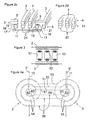
- Figure 2b shows the coupling coil 5 extending in a second plane 13 aligned with but spaced from the common plane 4 and the third plane 12.
- the second plane 13 extends between the common plane 4 and the third plane 12.
- the second terminal 7 of the first planar coil 2 extends by way of a via 14 to a metal pad (not shown) in the second plane 13 and then onto the first bridge track 10 by way of a second via 15.
- the second terminal 9 of the second planar coil 3 extends by way of a via 16 to a metal pad 19 (shown in Figure 2c ) in the second plane 13 and then onto the second bridge track 11 by way of a second via 17.
- the second bridge track 11 extends to a metal pad 19' in the second plane 13 by way of a via 17' and onto the connection point 9' in the common plate 4 by way of a via 16'.
- the closed coupling loop 5 comprises a first coil portion 20 arranged complementary to at least a part of the first planar coil 2 and a second coil portion 21 arranged complementary to at least a part of the second planar coil 3.
- the first and second coil portions 20, 21 are connected together by a connecting portion 22 to form a closed loop.
- Figure 2d which comprises section through B-B of Figure 2a , shows the tracks of the first coil 2 in the common plane 4 and the tracks of the first coil portion 20 of the coupling loop 5 arranged complementary to the first coil 2 in the second plane 13.
- the connecting portion comprises two connector tracks; a first connector track 23 and a second connector track 24 arranged to extend between the two coil portions 20, 21.
- first and second coil portions 20 and 21 track the first and second planar coils 2, 3, they are spirals and thus have outer spiral ends and inner spiral ends.
- the outer spiral ends of the first and second coil portions 20 and 21 are connected together by the first connector track 23, which extends in the same plane as the coil portions 20, 21 (the second plane 13 in this example).
- the second connector track 24, which connects to the inner spiral ends of the first and second coil portions 20 and 21 is required to traverse the first and second coil portions 20 and 21 in order to close the coupling loop 5. Accordingly, the second connector track 24 extends in a different plane to the remainder of the coupling loop 5 so that it can traverse the coils of the first and second coil portions.
- the closed coupling loop 5 is thus substantially planar and extends over a single plane except for a portion (the second connector track 24) that extends between the coil portions 20, 21.
- the second connector track 24, in this example, extends in the same plane as the bridge tracks 10, 11, which may be a top metal layer of a die (not shown).
- the common mode choke 1, in this example is provided over three metal layers of a silicon substrate.
- One or all of the substantially two-dimensional layer may be symmetrical about a line extending between planar coils.
- the common mode choke 1 extends in several layers it is also substantially symmetrical about a plane aligned with symmetry line SL that extends between the first and second planar coils 2, 3 and orthogonal to the common plane 4, the second plane 13 and the third plane 12.
- the common mode choke 1 is provided with a differentially signalled signal, which is provided over two lines.
- the first line is connected to the first terminal 6 and the second line is connected to the first terminal 8.
- the second terminal 7 comprises an output from the first coil 2 and the second terminal 9 provides an output from the second coil 3.
- the two lines of the differential data channel will see the same impedances when passing through the symmetric common mode choke 1. This may result in reduced data distortion compared to asymmetric layouts.
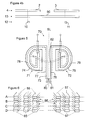
- Figures 3, 4a and 4b show a second example in which a plurality of coupling loops 50 are provided to electromagnetically couple the first and second planar coils.
- the same reference numerals have been used for identical parts.
- the first planar coil 2 and the second planar coil 3 have substantially the same layout as shown in Figure 2a . However, it will be appreciated that other planar coil shapes are possible. Further, the planar coils 2, 3 connect to first and second bridge tracks 10 and 11 to provide a connection point 7', 9' that is located outside the first and second planar coils 2, 3
- the coupling loops 50 each comprise closed loops and are each configured to electromagnetically couple the first and second planar coils 2, 3.
- three closed coupling loops 51, 52, 53 are provided.
- the three closed coupling loops 51, 52, 53 are, in this example, concentric.
- the loops 50 all lie in the same plane arranged one inside the other. It will be appreciated that in other embodiments, the coupling loops 50 may be provided in different planes or layers. For example, one or more closed coupling loops may extend in plane above the common plane 4 and one or more closed coupling loops may extend in plane below the common plane 4.
- the common mode choke 1 (comprising the planar coils 2, 3 and the coupling coils 50) is provided over two metal layers of a silicon substrate (as shown in Figure 4b ).
- the bridge tracks 10, 11 which connect to the first and second planar coils 2, 3 are provided in a third layer 12 but other connections to the second terminal 7 and the second terminal 9 are possible.
- Each closed coupling loop 51, 52, 53 comprises a first coil portion 54 arranged complementary to part of the first planar coil 2 and a second coil portion 55 arranged complementary to part of the second planar coil 3.
- the first and second coil portions 54, 55 are connected together by a connecting portion 56 to form a closed loop.
- the connecting portion 56 comprises a first track 57 and a second track 58.
- the first track 57 is configured to connect a first end 60 of the first coil portion 54 to a complementary first end 61 of the second coil portion 55 and the second track 58 is configured to connect a second end 62 of the first coil portion 54 to a complementary second end 63 of the second coil portion 55.
- the first and second tracks 57, 58 of the connecting portion 56 extend in the same plane 13.
- the first coil portion 54 comprises less than one turn and tracks part of the first planar coil 2.
- the second coil portion 55 comprises less than one turn and tracks part of the second planar coil 3.
- the number of coupling coils may be sufficient to track each turn or part turn of the planar coils 2, 3.
- the first and second planar coils 2, 3 have approximately 2.5 turns and thus three coil turns intersect a radially extending plane centred on the planar coils 2, 3 at at least one radial position. Accordingly, an equivalent number (three) of coupling coils 50 are provided. It will be appreciated that other numbers of a coupling coils 50 may be provided, which may or may not be related to the number of turns of the first and/or second planar coils 2, 3.
- Figure 5 shows a further example layout comprising a symmetrical common mode choke 70.
- the same reference numerals have been used for identical parts.
- the first and second planar coils 71, 72 have a different shape.
- the first planar coil 71 includes a straight section 73 and a coiled section 74.
- the second planar coil 72 includes a straight section 75 and a coiled section 76.
- the first and second planar coils are mirror images of one another and accordingly coil in opposite directions (anti-clockwise and clockwise respectively for example).
- the straight sections 73, 75 of the first and second planar coils 71, 72 are arranged parallel to one another adjacent a line of symmetry SL of the common mode choke 70.
- a single coupling coil 77 is provided and comprises a closed loop.
- the coupling coil 77 is shown in dashed lines in Figure 5 and alongside the first and second planar coils 71, 72. However, it will be appreciated that the coupling coil 77 is arranged in an adjacent plane aligned with but spaced from the plane in which the first and second planar coils lie.
- the coupling coil 77 comprises a first coil portion 78 and a second coil portion 79 connected together by a connecting portion 80.
- the connecting portion 80 comprises two connector tracks; a first connector track 81 and a second connector track 82 arranged to extend between the two coil portions 78, 79.
- the first and second coil portions 78 and 79 track the first and second planar coils 71, 72 (in their adjacent plane or layer) and thus they are spirals and have outer spiral ends and inner spiral ends.
- the outer spiral ends of the first and second coil portions 78 and 79 are connected together by the first connector track 81, which extends in the same plane as the coil portions 78, 79 (the second plane 13 in this example).
- the second connector track 82 which connects to the inner spiral ends of the first and second coil portions 78 and 79 is required to traverse the first and second coil portions 78 and 79 in order to close the coupling loop 5.
- the second connector track 82 extends in a different plane to the remainder of the coupling loop 77 so that it can traverse the coils of the first and second coil portions 78, 79.
- the closed coupling loop 77 is thus substantially planar and extends over a single plane except for a portion (the second connector track 82) that extends between the coil portions.
- the second connector track is shown schematically and in practice may have a layout closer to that described for the second connector track 24 of Figures 2a and 2b .
- Figure 6 shows a sectional view through part of a first planar coil 85 and a closed coupling loop 86 and an equivalent part of a second planar coil 87. Only the outermost turns of each of the coils/loop 85, 86, 87 are shown.
- the first planar coil 85 extends over two planes A, D (connected by vias between the layers (not shown)).
- Corresponding but mirror image parts of the second planar coil 87 extend over the planes A, D.
- the first and second planar coils thus extend over common planes.
- the first and second planar coils can be each considered to comprise a first part that extends in a first plane and a second part that extends in a second plane.
- the corresponding parts are substantially mirror images of one another and the corresponding parts each extend in common planes.
- the first part of the first planar coil 85 extends in common plane A with the corresponding first part of the second planar coil 86.
- the second part of the first planar coil 85 extends in common plane D with the corresponding second part of the second planar coil 86.
- the closed coupling loop 86 may also extend over two planes B, C to magnetically couple the first and second parts of the first and second planar coils 85, 86. It will be appreciated that the relative positions of the first and second planar coils 85, 87 and the closed coupling loop in the planes A-D may be different provided that corresponding parts, i.e. mirror image parts, of each of the first and second planar coils lie in common planes.
- Figure 7 shows a further example common mode choke in which the first planar coil, second planar coil, the closed coupling loop and bridge tracks are provided in only two layers.
- the first planar coil 88 and the second planar coil 89 are provided in a single common plane, which comprises a first layer.
- the first planar coil includes an outer spiral end 88a and in inner spiral end 88b.
- the second planar coil includes an outer spiral end 89a and an inner spiral end 89b.
- the closed coupling loop 90 shown in dotted lines, comprises a plurality of loops (two) 90a, 90b.
- the closed coupling loop 90 is formed in a second layer, parallel to and spaced from the first layer.
- the closed coupling loop 90 and first and second planar coils 88, 89 are shown in figure 7 as extending side by side (for clarity) they, in fact, directly overlie one another in the parallel first and second layers.
- the closed coupling loops 90 are configured to extend inwardly, in plan view, of the inner spiral ends 88b, 89b.
- the closed coupling loops each include a divergent section 93, 94 in which they leave a path that substantially tracks the first planar coil or second planar coil such that they extend inwardly of the inner spiral ends 88b, 89b.
- bridge tracks 91, 92 which connect the inner spiral ends 89a, 89b to outside the plan of the spiral coils 88, 89, are able to extend in the same plane as the closed coupling loop 90.
- first and second planar coils 88, 89 in this example are of spiral shape but extend in an annular region rather than spiralling to a point central to the spiral.
- Figure 8 shows part of an example common mode choke in which the first and second planar coils are wound bifilar with the closed coupling loop.
- the closed coupling loop is shown in a different layer to the first and second planar coils, in this example the first planar coil is inter-wound with the closed coupling loop and the second planar coil is inter-wound with the closed coupling loop.
- Figure 8 shows the first planar coil 95 inter-wound with the closed coupling loop 96. Three turns of the first planar coil 95 are shown and two turns of the closed coupling loop 96.
- Figure 9 shows an electronic device 100 which may comprise a transmitter or receiver of a telecommunications network.
- the device 100 includes a common mode choke 101 as described in any of the examples above.
- the first planar coil 2, 71 receives a first line of a differentially signalled input signal received over two signal lines 102 and the second planar coil 3, 72 receives a second line of the differentially signalled input signal received over the two signal lines 102.
- the first and second planar coils 2, 71, 3, 72 provide a differentially signalled output signal over two signal lines 103.
- the electronic device 100 may include other electronic components, for signal processing for example.
Landscapes
- Engineering & Computer Science (AREA)
- Power Engineering (AREA)
- Microelectronics & Electronic Packaging (AREA)
- Coils Or Transformers For Communication (AREA)
Abstract
Description
- This disclosure relates to a common mode choke. In particular, it relates to a planar, metal on silicon common mode choke configured to operate on a differential signal. The disclosure also relates to an electronic device that utilises the common mode choke to filter a signal.
- According to a first aspect we provide a common mode choke comprising a first planar coil for receiving a first signal, a second planar coil for receiving a second signal, the first and second coils comprising substantially mirror images of one another and arranged side by side in a common plane, the first planar coil and second planar coil electromagnetically coupled by a closed coupling loop.
- This is advantageous as by providing the first and second planar coils side-by-side rather than face to face, the planar coils (the signal receiving coils) of the common mode choke can be arranged symmetrically. Thus, the closed coupling loop provides for the magnetic coupling of the planar coils.
- The closed coupling loop may be substantially planar and configured to extend, at least in part, in a plane adjacent but spaced from the common plane. This arrangement is advantageous as the common mode choke may be provided in a plurality of metal layers in a silicon substrate, for example. The closed coupling loop may be symmetrical. The closed coupling loop may extend in the common plane alongside the first planar coil and the second planar coil.
- The closed coupling loop may comprise a first coil portion arranged complementary to at least a portion of the first planar coil, a second coil portion arranged complementary to at least a portion of the second planar coil and a connecting portion arranged to connect the first and second coil portions to form a closed loop. Thus, the coil portions may be configured to track the planar coils to magnetically couple thereto and the connecting portion provides the link between the coil portions to magnetically couple the planar coils together.
- The connecting portion comprises a first track and a second track, the first track configured to connect a first end of the first coil portion to a complementary first end of the second coil portion and the second track configured to connect a second end of the first coil portion to a complementary second end of the second coil portion, the first and second tracks configured to extend in different planes.
- The connecting portion may comprise a first track and a second track, the first track configured to connect a first end of the first coil portion to a complementary first end of the second coil portion and the second track configured to connect a second end of the first coil portion to a complementary second end of the second coil portion, the first and second tracks configured to extend in the same plane. This is advantageous as the common mode choke may be provided over two metal layers.
- The common mode choke may be symmetrical about a plane extending between the first and second planar coils. A symmetrical common mode choke may provide low signal distortion.
- A plurality of closed coupling loops may be provided each configured to electromagnetically couple the first and second planar coils. Thus, each closed coupling loop may be complementary to only part of the first planar coil and to only part of the second planar coil, with each of the closed coupling loops covering a different part of the first and second coils.
- At least two of the plurality of closed coupling loops may extend in the same plane. Optionally, all of the closed coupling loops extend in the same plane.
- A first of the plurality of closed coupling loops may extend in plane above the common plane and a second of the plurality of closed coupling loops extends in plane below the common plane.
- The first planar coil may include a straight section and a coiled section and the second planar coil may include a straight section and a coiled section, wherein the straight sections of the first and second planar coils are arranged parallel to one another.
- The number of closed coupling loops may be equal to or one greater than the number of turns of the first or second planar coil.
- The first and/or second planar coils may comprise spirals and have an outer spiral end and an inner spiral end arranged in the common plane. The or each inner spiral end may connect to a bridge track that extends in a plane adjacent to but spaced from the common plane to provide a connection point that lies outside of the spiral.
- The first and second planar coils may comprise at least 1.5 turns or at least 2 turns or at least 2.5 turns.
- The first planar coil and the second planar coil may be each arranged over a plurality of parallel planes, with corresponding parts of the first planar coil and the second planar coil arranged in common planes of the plurality of parallel planes. Thus, the first and second planar coil parts that extend in common planes are substantially mirror images of one another. The closed coupling loop may or may not extend in a plane different to the first and second planar coils.
- The first and second planar coils may be spirals and each may have an outer spiral end and an inner spiral end and the common mode choke, including the closed coupling loop, may extend over only three layers including bridge tracks to provide a connection between the inner spiral ends and a point outside the spirals. Alternatively, the first and second planar coils may be spirals and each may have an outer spiral end and an inner spiral end and the common mode choke, including the closed coupling loop, may extend over only two layers including bridge tracks to provide a connection between the inner ends and a point outside the spirals.
- According to a further aspect we provide an electronic device including the common mode choke of the first aspect.
- The electronic device may comprise a transmitter or a receiver configured to transmit or receive a signal arranged over two signal channels wherein the first planar coil of the common mode choke is configured to connect to one of the two signal channels and the second planar coil of the common mode choke is configured to connect to the other of the two signal channels.
- There now follows, by way of example only, a detailed description of embodiments of the disclosure with reference to the following figures, in which:
-
Figure 1 shows a diagram representative of an example common mode choke; -
Figure 2a shows a plan view of the layout of the example common mode choke represented inFigure 1 ; -
Figure 2b shows a side view of the layout ofFigure 2a ; -
Figure 2c shows a perspective view of a cross section through A-A of the layout ofFigure 2a ; -
Figure 2d shows a perspective view of a cross section through B-B of the layout ofFigure 2a ; -
Figure 3 shows a diagram representative of a second example common mode choke; -
Figure 4a shows a plan view of the layout of the second example common mode choke represented inFigure 3 ; -
Figure 4b shows a side view of the layout ofFigure 4a ; -
Figure 5 shows a diagram representative of a third example common mode choke; -
Figure 6 shows an example common mode choke in which the first and second planar coils extend in more than one parallel plane; -
Figure 7 shows an example common mode choke formed in only two layers; -
Figure 8 shows an example common mode choke in which the first and second planar coils have a bifilar arrangement with the closed coupling loop; and -
Figure 9 shows an example electronic device. -
Figures 1 and 2a show acommon mode choke 1 having a firstplanar coil 2 forming a first signal channel and a secondplanar coil 3 forming a second signal channel. The first signal channel is configured to receive a first signal and the second signal channel is configured to receive a second signal. The first signal and second signal comprise component parts of a differentially transmitted signal. Thecommon mode choke 1 is configured to receive the differential signal over the two signal channels and attenuate common mode signals thereof and allow the differential signals to pass. - The first
planar coil 2 and the secondplanar coil 3 are substantially mirror images of one another and arranged side by side in acommon plane 4. The firstplanar coil 2 and secondplanar coil 3 are electromagnetically coupled to one another by a closedcoupling loop 5. Thecommon mode choke 1 is substantially symmetrical along a plane SL that extends between the first and secondplanar coils common mode choke 1 may have advantages over asymmetrical common mode chokes. - The first
planar coil 2 and the secondplanar coil 3 are formed as a track in a metal layer on a substrate, such as a silicon substrate. Thecoils coils planar coils planar coil 2 includes afirst terminal 6 and asecond terminal 7. The first andsecond terminals planar coil 3 includes afirst terminal 8 and asecond terminal 9. The first andsecond terminals - The
second terminal 7 of the first planar coil and thesecond terminal 9 of the secondplanar coil 3 may be configured to connect to a respective first andsecond bridge track Figure 2c ) to thesecond terminals planar coils third plane 12, aligned with but spaced from thecommon plane 4. In some examples, the bridge tracks 10, 11 may be provided in a top metal layer of a die (not shown) in which the common mode choke is formed. - The
coupling loop 5 comprises a closed loop and is thus short circuited. Thecoupling loop 5, although shown extending slightly alongside the first and secondplanar coils figure 2a , is, in fact, configured to extend in a different plane and follow the first and secondplanar coils Figure 2b shows thecoupling coil 5 extending in asecond plane 13 aligned with but spaced from thecommon plane 4 and thethird plane 12. Thesecond plane 13 extends between thecommon plane 4 and thethird plane 12. Thus, thesecond terminal 7 of the firstplanar coil 2 extends by way of a via 14 to a metal pad (not shown) in thesecond plane 13 and then onto thefirst bridge track 10 by way of a second via 15. Likewise, thesecond terminal 9 of the secondplanar coil 3 extends by way of a via 16 to a metal pad 19 (shown inFigure 2c ) in thesecond plane 13 and then onto thesecond bridge track 11 by way of a second via 17. With reference toFigure 2c , thesecond bridge track 11 extends to a metal pad 19' in thesecond plane 13 by way of a via 17' and onto the connection point 9' in thecommon plate 4 by way of a via 16'. - The
closed coupling loop 5 comprises afirst coil portion 20 arranged complementary to at least a part of the firstplanar coil 2 and asecond coil portion 21 arranged complementary to at least a part of the secondplanar coil 3. The first andsecond coil portions portion 22 to form a closed loop.Figure 2d , which comprises section through B-B ofFigure 2a , shows the tracks of thefirst coil 2 in thecommon plane 4 and the tracks of thefirst coil portion 20 of thecoupling loop 5 arranged complementary to thefirst coil 2 in thesecond plane 13. Thus, the tracks in different planes may be aligned. The connecting portion comprises two connector tracks; afirst connector track 23 and asecond connector track 24 arranged to extend between the twocoil portions second coil portions planar coils second coil portions first connector track 23, which extends in the same plane as thecoil portions 20, 21 (thesecond plane 13 in this example). Thesecond connector track 24, which connects to the inner spiral ends of the first andsecond coil portions second coil portions coupling loop 5. Accordingly, thesecond connector track 24 extends in a different plane to the remainder of thecoupling loop 5 so that it can traverse the coils of the first and second coil portions. Theclosed coupling loop 5 is thus substantially planar and extends over a single plane except for a portion (the second connector track 24) that extends between thecoil portions second connector track 24, in this example, extends in the same plane as the bridge tracks 10, 11, which may be a top metal layer of a die (not shown). Thus, thecommon mode choke 1, in this example, is provided over three metal layers of a silicon substrate. One or all of the substantially two-dimensional layer may be symmetrical about a line extending between planar coils. Further, as thecommon mode choke 1 extends in several layers it is also substantially symmetrical about a plane aligned with symmetry line SL that extends between the first and secondplanar coils common plane 4, thesecond plane 13 and thethird plane 12. - In use, the
common mode choke 1 is provided with a differentially signalled signal, which is provided over two lines. The first line is connected to thefirst terminal 6 and the second line is connected to thefirst terminal 8. Thesecond terminal 7 comprises an output from thefirst coil 2 and thesecond terminal 9 provides an output from thesecond coil 3. The two lines of the differential data channel will see the same impedances when passing through the symmetriccommon mode choke 1. This may result in reduced data distortion compared to asymmetric layouts. -
Figures 3, 4a and4b show a second example in which a plurality ofcoupling loops 50 are provided to electromagnetically couple the first and second planar coils. The same reference numerals have been used for identical parts. The firstplanar coil 2 and the secondplanar coil 3 have substantially the same layout as shown inFigure 2a . However, it will be appreciated that other planar coil shapes are possible. Further, theplanar coils planar coils - The
coupling loops 50 each comprise closed loops and are each configured to electromagnetically couple the first and secondplanar coils closed coupling loops closed coupling loops loops 50 all lie in the same plane arranged one inside the other. It will be appreciated that in other embodiments, thecoupling loops 50 may be provided in different planes or layers. For example, one or more closed coupling loops may extend in plane above thecommon plane 4 and one or more closed coupling loops may extend in plane below thecommon plane 4. However, in this example, the common mode choke 1 (comprising theplanar coils Figure 4b ). The bridge tracks 10, 11 which connect to the first and secondplanar coils third layer 12 but other connections to thesecond terminal 7 and thesecond terminal 9 are possible. - Each
closed coupling loop first coil portion 54 arranged complementary to part of the firstplanar coil 2 and asecond coil portion 55 arranged complementary to part of the secondplanar coil 3. The first andsecond coil portions portion 56 to form a closed loop. The connectingportion 56 comprises afirst track 57 and asecond track 58. Thefirst track 57 is configured to connect afirst end 60 of thefirst coil portion 54 to a complementaryfirst end 61 of thesecond coil portion 55 and thesecond track 58 is configured to connect asecond end 62 of thefirst coil portion 54 to a complementarysecond end 63 of thesecond coil portion 55. Unlike the first example described above, the first andsecond tracks portion 56 extend in thesame plane 13. - The
first coil portion 54 comprises less than one turn and tracks part of the firstplanar coil 2. Likewise, thesecond coil portion 55 comprises less than one turn and tracks part of the secondplanar coil 3. The number of coupling coils may be sufficient to track each turn or part turn of theplanar coils planar coils planar coils planar coils -
Figure 5 shows a further example layout comprising a symmetricalcommon mode choke 70. The same reference numerals have been used for identical parts. In this example the first and secondplanar coils planar coil 71 includes astraight section 73 and acoiled section 74. Likewise, the secondplanar coil 72 includes astraight section 75 and acoiled section 76. The first and second planar coils are mirror images of one another and accordingly coil in opposite directions (anti-clockwise and clockwise respectively for example). Thestraight sections planar coils common mode choke 70. - A
single coupling coil 77 is provided and comprises a closed loop. Thecoupling coil 77 is shown in dashed lines inFigure 5 and alongside the first and secondplanar coils coupling coil 77 is arranged in an adjacent plane aligned with but spaced from the plane in which the first and second planar coils lie. As in the example shown in relation toFigure 2a , thecoupling coil 77 comprises afirst coil portion 78 and asecond coil portion 79 connected together by a connectingportion 80. The connectingportion 80 comprises two connector tracks; afirst connector track 81 and asecond connector track 82 arranged to extend between the twocoil portions second coil portions planar coils 71, 72 (in their adjacent plane or layer) and thus they are spirals and have outer spiral ends and inner spiral ends. The outer spiral ends of the first andsecond coil portions first connector track 81, which extends in the same plane as thecoil portions 78, 79 (thesecond plane 13 in this example). Thesecond connector track 82, which connects to the inner spiral ends of the first andsecond coil portions second coil portions coupling loop 5. Accordingly, thesecond connector track 82 extends in a different plane to the remainder of thecoupling loop 77 so that it can traverse the coils of the first andsecond coil portions closed coupling loop 77 is thus substantially planar and extends over a single plane except for a portion (the second connector track 82) that extends between the coil portions. InFigure 5 , the second connector track is shown schematically and in practice may have a layout closer to that described for thesecond connector track 24 ofFigures 2a and 2b . -
Figure 6 shows a sectional view through part of a firstplanar coil 85 and aclosed coupling loop 86 and an equivalent part of a secondplanar coil 87. Only the outermost turns of each of the coils/loop planar coil 85 extends over two planes A, D (connected by vias between the layers (not shown)). Corresponding but mirror image parts of the secondplanar coil 87 extend over the planes A, D. The first and second planar coils thus extend over common planes. The first and second planar coils can be each considered to comprise a first part that extends in a first plane and a second part that extends in a second plane. The corresponding parts are substantially mirror images of one another and the corresponding parts each extend in common planes. Thus, the first part of the firstplanar coil 85 extends in common plane A with the corresponding first part of the secondplanar coil 86. Likewise, the second part of the firstplanar coil 85 extends in common plane D with the corresponding second part of the secondplanar coil 86. Theclosed coupling loop 86 may also extend over two planes B, C to magnetically couple the first and second parts of the first and secondplanar coils planar coils -
Figure 7 shows a further example common mode choke in which the first planar coil, second planar coil, the closed coupling loop and bridge tracks are provided in only two layers. In particular, the firstplanar coil 88 and the secondplanar coil 89 are provided in a single common plane, which comprises a first layer. The first planar coil includes an outerspiral end 88a and in innerspiral end 88b. Likewise, the second planar coil includes an outer spiral end 89a and an innerspiral end 89b. The closed coupling loop 90, shown in dotted lines, comprises a plurality of loops (two) 90a, 90b. The closed coupling loop 90 is formed in a second layer, parallel to and spaced from the first layer. Thus, although the closed coupling loop 90 and first and secondplanar coils figure 7 as extending side by side (for clarity) they, in fact, directly overlie one another in the parallel first and second layers. The closed coupling loops 90 are configured to extend inwardly, in plan view, of the inner spiral ends 88b, 89b. In particular, the closed coupling loops each include adivergent section planar coils -
Figure 8 shows part of an example common mode choke in which the first and second planar coils are wound bifilar with the closed coupling loop. Thus, while inFigure 2a described above the closed coupling loop is shown in a different layer to the first and second planar coils, in this example the first planar coil is inter-wound with the closed coupling loop and the second planar coil is inter-wound with the closed coupling loop. Thus, in section the coils and the closed coupling loop extend in the same plane albeit for any bridge tracks.Figure 8 shows the firstplanar coil 95 inter-wound with theclosed coupling loop 96. Three turns of the firstplanar coil 95 are shown and two turns of theclosed coupling loop 96. -
Figure 9 shows anelectronic device 100 which may comprise a transmitter or receiver of a telecommunications network. Thedevice 100 includes acommon mode choke 101 as described in any of the examples above. The firstplanar coil signal lines 102 and the secondplanar coil signal lines 102. The first and secondplanar coils signal lines 103. It will be appreciated that theelectronic device 100 may include other electronic components, for signal processing for example.
Claims (15)
- A common mode choke comprising a first planar coil for receiving a first signal, a second planar coil for receiving a second signal, the first and second coils comprising substantially mirror images of one another and arranged side by side in a common plane, the first planar coil and second planar coil electromagnetically coupled by a closed coupling loop.
- A common mode choke according to claim 1, in which the closed coupling loop is planar and configured to extend at least in part in a plane adjacent to but spaced from the common plane.
- A common mode choke according to claim 1 or claim 2, in which the closed coupling loop comprises a first coil portion arranged complementary to at least a portion of the first planar coil, a second coil portion arranged complementary to at least a portion of the second planar coil and a connecting portion arranged to connect the first and second coil portions to form a closed loop.
- A common mode choke according to claim 3, in which the connecting portion comprises a first track and a second track, the first track configured to connect a first end of the first coil portion to a complementary first end of the second coil portion and the second track configured to connect a second end of the first coil portion to a complementary second end of the second coil portion, the first and second tracks configured to extend in the same plane.
- A common mode choke according to claim 3, in which the connecting portion comprises a first track and a second track, the first track configured to connect a first end of the first coil portion to a complementary first end of the second coil portion and the second track configured to connect a second end of the first coil portion to a complementary second end of the second coil portion, the first and second tracks configured to extend in different planes.
- A common mode choke according to any preceding claim, in which the common mode choke is symmetrical about a plane extending between the first and second planar coils.
- A common mode choke according to any preceding claim, in which a plurality of closed coupling loops are provided each configured to electromagnetically couple the first and second planar coils.
- A common mode choke according to claim 7, in which at least two of the plurality of closed coupling loops extend in the same plane.
- A common mode choke according to claim 7, in which a first of the plurality of closed coupling loops extends in plane above the common plane and a second of the plurality of closed coupling loops extends in plane below the common plane.
- A common mode choke according to any preceding claim, in which the first planar coil includes a straight section and a coiled section and the second planar coil includes a straight section and a coiled section, wherein the straight sections of the first and second planar coils are arranged parallel to one another.
- A common mode choke according to any one of claims 7 to 9, in which the number of closed coupling loops is equal to or one greater than the number of turns of the first or second planar coil.
- A common mode choke according to any preceding claim, in which the first and/or second planar coils comprise spirals and have an outer spiral end and an inner spiral end arranged in the common plane and wherein the or each inner spiral end connects to a bridge track that extends in a plane adjacent to but spaced from the common plane to provide a connection point that lies outside of the spiral.
- A common mode choke according to any preceding claim, in which the first planar coil and the second planar coil are each arranged over a plurality of parallel planes, with corresponding parts of the first planar coil and the second planar coil arranged in common planes of the plurality of parallel planes.
- An electronic device including the common mode choke of any preceding claim.
- An electronic device according to claim 14 comprising a transmitter or a receiver configured to transmit or receive a signal arranged over two signal channels wherein the first planar coil of the common mode choke is configured to connect to one of the two signal channels and the second planar coil of the common mode choke is configured to connect to the other of the two signal channels.
Priority Applications (3)
| Application Number | Priority Date | Filing Date | Title |
|---|---|---|---|
| EP15151828.9A EP3048618B1 (en) | 2015-01-20 | 2015-01-20 | Common mode choke |
| US14/984,614 US10096419B2 (en) | 2015-01-20 | 2015-12-30 | Common mode choke |
| CN201610034290.0A CN105810385B (en) | 2015-01-20 | 2016-01-19 | common mode choke |
Applications Claiming Priority (1)
| Application Number | Priority Date | Filing Date | Title |
|---|---|---|---|
| EP15151828.9A EP3048618B1 (en) | 2015-01-20 | 2015-01-20 | Common mode choke |
Publications (2)
| Publication Number | Publication Date |
|---|---|
| EP3048618A1 true EP3048618A1 (en) | 2016-07-27 |
| EP3048618B1 EP3048618B1 (en) | 2019-05-29 |
Family
ID=52354846
Family Applications (1)
| Application Number | Title | Priority Date | Filing Date |
|---|---|---|---|
| EP15151828.9A Active EP3048618B1 (en) | 2015-01-20 | 2015-01-20 | Common mode choke |
Country Status (3)
| Country | Link |
|---|---|
| US (1) | US10096419B2 (en) |
| EP (1) | EP3048618B1 (en) |
| CN (1) | CN105810385B (en) |
Cited By (1)
| Publication number | Priority date | Publication date | Assignee | Title |
|---|---|---|---|---|
| US20220165476A1 (en) * | 2020-11-20 | 2022-05-26 | Analog Devices International Unlimited Company | Symmetric split transformer for emi reduction |
Families Citing this family (2)
| Publication number | Priority date | Publication date | Assignee | Title |
|---|---|---|---|---|
| CN107871594B (en) * | 2017-05-31 | 2019-07-02 | 洪豪立 | Taiji type graphene filter choke coil and its manufacturing method |
| US20240186054A1 (en) * | 2022-10-25 | 2024-06-06 | Delta Electronics, Inc. | Isolated power supply for gate driver |
Citations (2)
| Publication number | Priority date | Publication date | Assignee | Title |
|---|---|---|---|---|
| JP2007266140A (en) * | 2006-03-27 | 2007-10-11 | Aw Japan:Kk | Line filter having flat structure |
| US20130181803A1 (en) * | 2012-01-16 | 2013-07-18 | Telefonaktiebolaget Lm Ericsson (Publ) | Wideband multilayer transmission line transformer |
Family Cites Families (13)
| Publication number | Priority date | Publication date | Assignee | Title |
|---|---|---|---|---|
| US4425511A (en) * | 1981-02-09 | 1984-01-10 | Amnon Brosh | Planar coil apparatus employing a stationary and a movable board |
| EP0507360B1 (en) * | 1991-01-30 | 1996-05-08 | The Boeing Company | Current mode bus coupler with planar coils and shields |
| JP3484971B2 (en) * | 1998-03-19 | 2004-01-06 | 松下電器産業株式会社 | Common mode choke coil |
| US6097273A (en) * | 1999-08-04 | 2000-08-01 | Lucent Technologies Inc. | Thin-film monolithic coupled spiral balun transformer |
| US6653910B2 (en) * | 2001-12-21 | 2003-11-25 | Motorola, Inc. | Spiral balun |
| US6842158B2 (en) * | 2001-12-27 | 2005-01-11 | Skycross, Inc. | Wideband low profile spiral-shaped transmission line antenna |
| JP2006093603A (en) * | 2004-09-27 | 2006-04-06 | Mitsubishi Materials Corp | Multilayer common mode choke coil array |
| JP2006261585A (en) * | 2005-03-18 | 2006-09-28 | Tdk Corp | Common mode choke coil |
| JP4835751B2 (en) * | 2007-05-14 | 2011-12-14 | 株式会社村田製作所 | Common mode choke coil |
| JP5073373B2 (en) * | 2007-06-08 | 2012-11-14 | Tdk株式会社 | Common mode choke coil |
| US8044759B2 (en) * | 2008-01-08 | 2011-10-25 | Samsung Electro-Mechanics | Overlapping compact multiple transformers |
| US8593244B2 (en) * | 2008-09-18 | 2013-11-26 | The Boeing Company | Control of leakage inductance |
| EP2814113B1 (en) * | 2013-06-14 | 2019-08-07 | Ampleon Netherlands B.V. | Marchand balun and power amplifier using the same |
-
2015
- 2015-01-20 EP EP15151828.9A patent/EP3048618B1/en active Active
- 2015-12-30 US US14/984,614 patent/US10096419B2/en active Active
-
2016
- 2016-01-19 CN CN201610034290.0A patent/CN105810385B/en active Active
Patent Citations (2)
| Publication number | Priority date | Publication date | Assignee | Title |
|---|---|---|---|---|
| JP2007266140A (en) * | 2006-03-27 | 2007-10-11 | Aw Japan:Kk | Line filter having flat structure |
| US20130181803A1 (en) * | 2012-01-16 | 2013-07-18 | Telefonaktiebolaget Lm Ericsson (Publ) | Wideband multilayer transmission line transformer |
Cited By (1)
| Publication number | Priority date | Publication date | Assignee | Title |
|---|---|---|---|---|
| US20220165476A1 (en) * | 2020-11-20 | 2022-05-26 | Analog Devices International Unlimited Company | Symmetric split transformer for emi reduction |
Also Published As
| Publication number | Publication date |
|---|---|
| EP3048618B1 (en) | 2019-05-29 |
| US10096419B2 (en) | 2018-10-09 |
| CN105810385A (en) | 2016-07-27 |
| CN105810385B (en) | 2017-09-22 |
| US20160211068A1 (en) | 2016-07-21 |
Similar Documents
| Publication | Publication Date | Title |
|---|---|---|
| US11373795B2 (en) | Transformer device | |
| CN111755227B (en) | Inductance device | |
| US10636561B2 (en) | Common mode noise filter | |
| US11515072B2 (en) | Inductor device | |
| JP6526075B2 (en) | Magnetic core used in wireless power transfer system | |
| US7812701B2 (en) | Compact multiple transformers | |
| US7924135B2 (en) | Transformer | |
| US6717502B2 (en) | Integrated balun and transformer structures | |
| US8044759B2 (en) | Overlapping compact multiple transformers | |
| US10559415B2 (en) | Common mode filter capable of balancing induced inductance and distributed capacitance | |
| US10366821B2 (en) | Common mode noise filter | |
| US10305441B2 (en) | Common mode noise filter | |
| US20200082977A1 (en) | Transformer and signal transmission system | |
| US10778177B2 (en) | Common mode noise filter | |
| US10096419B2 (en) | Common mode choke | |
| JP2006286884A (en) | Common mode choke coil | |
| CN107527728A (en) | Common-mode noise filter | |
| KR20190046664A (en) | Balanced-to-unbalanced (balun) transformer | |
| US20190148064A1 (en) | Inductive coupling system and communication system | |
| US20180190423A1 (en) | Common mode choke coil | |
| JP6421896B2 (en) | Phase shifter module, multiplexer / demultiplexer, and communication device | |
| CN107731485B (en) | Semiconductor device with a plurality of semiconductor chips | |
| CN114724820B (en) | Transformer | |
| EP4374140A1 (en) | High-layer excitation coil for inductive position sensor | |
| JP2010081185A (en) | Directional coupler and transmitter/receiver |
Legal Events
| Date | Code | Title | Description |
|---|---|---|---|
| PUAI | Public reference made under article 153(3) epc to a published international application that has entered the european phase |
Free format text: ORIGINAL CODE: 0009012 |
|
| AK | Designated contracting states |
Kind code of ref document: A1 Designated state(s): AL AT BE BG CH CY CZ DE DK EE ES FI FR GB GR HR HU IE IS IT LI LT LU LV MC MK MT NL NO PL PT RO RS SE SI SK SM TR |
|
| AX | Request for extension of the european patent |
Extension state: BA ME |
|
| RAP1 | Party data changed (applicant data changed or rights of an application transferred) |
Owner name: NEXPERIA B.V. |
|
| STAA | Information on the status of an ep patent application or granted ep patent |
Free format text: STATUS: REQUEST FOR EXAMINATION WAS MADE |
|
| 17P | Request for examination filed |
Effective date: 20170127 |
|
| RBV | Designated contracting states (corrected) |
Designated state(s): AL AT BE BG CH CY CZ DE DK EE ES FI FR GB GR HR HU IE IS IT LI LT LU LV MC MK MT NL NO PL PT RO RS SE SI SK SM TR |
|
| RAP1 | Party data changed (applicant data changed or rights of an application transferred) |
Owner name: NEXPERIA B.V. |
|
| GRAP | Despatch of communication of intention to grant a patent |
Free format text: ORIGINAL CODE: EPIDOSNIGR1 |
|
| STAA | Information on the status of an ep patent application or granted ep patent |
Free format text: STATUS: GRANT OF PATENT IS INTENDED |
|
| INTG | Intention to grant announced |
Effective date: 20190206 |
|
| GRAS | Grant fee paid |
Free format text: ORIGINAL CODE: EPIDOSNIGR3 |
|
| GRAA | (expected) grant |
Free format text: ORIGINAL CODE: 0009210 |
|
| STAA | Information on the status of an ep patent application or granted ep patent |
Free format text: STATUS: THE PATENT HAS BEEN GRANTED |
|
| AK | Designated contracting states |
Kind code of ref document: B1 Designated state(s): AL AT BE BG CH CY CZ DE DK EE ES FI FR GB GR HR HU IE IS IT LI LT LU LV MC MK MT NL NO PL PT RO RS SE SI SK SM TR |
|
| REG | Reference to a national code |
Ref country code: GB Ref legal event code: FG4D |
|
| REG | Reference to a national code |
Ref country code: CH Ref legal event code: EP |
|
| REG | Reference to a national code |
Ref country code: DE Ref legal event code: R096 Ref document number: 602015031027 Country of ref document: DE |
|
| REG | Reference to a national code |
Ref country code: AT Ref legal event code: REF Ref document number: 1138755 Country of ref document: AT Kind code of ref document: T Effective date: 20190615 |
|
| REG | Reference to a national code |
Ref country code: IE Ref legal event code: FG4D |
|
| REG | Reference to a national code |
Ref country code: NL Ref legal event code: MP Effective date: 20190529 |
|
| REG | Reference to a national code |
Ref country code: LT Ref legal event code: MG4D |
|
| PG25 | Lapsed in a contracting state [announced via postgrant information from national office to epo] |
Ref country code: FI Free format text: LAPSE BECAUSE OF FAILURE TO SUBMIT A TRANSLATION OF THE DESCRIPTION OR TO PAY THE FEE WITHIN THE PRESCRIBED TIME-LIMIT Effective date: 20190529 Ref country code: PT Free format text: LAPSE BECAUSE OF FAILURE TO SUBMIT A TRANSLATION OF THE DESCRIPTION OR TO PAY THE FEE WITHIN THE PRESCRIBED TIME-LIMIT Effective date: 20190930 Ref country code: SE Free format text: LAPSE BECAUSE OF FAILURE TO SUBMIT A TRANSLATION OF THE DESCRIPTION OR TO PAY THE FEE WITHIN THE PRESCRIBED TIME-LIMIT Effective date: 20190529 Ref country code: LT Free format text: LAPSE BECAUSE OF FAILURE TO SUBMIT A TRANSLATION OF THE DESCRIPTION OR TO PAY THE FEE WITHIN THE PRESCRIBED TIME-LIMIT Effective date: 20190529 Ref country code: ES Free format text: LAPSE BECAUSE OF FAILURE TO SUBMIT A TRANSLATION OF THE DESCRIPTION OR TO PAY THE FEE WITHIN THE PRESCRIBED TIME-LIMIT Effective date: 20190529 Ref country code: AL Free format text: LAPSE BECAUSE OF FAILURE TO SUBMIT A TRANSLATION OF THE DESCRIPTION OR TO PAY THE FEE WITHIN THE PRESCRIBED TIME-LIMIT Effective date: 20190529 Ref country code: NO Free format text: LAPSE BECAUSE OF FAILURE TO SUBMIT A TRANSLATION OF THE DESCRIPTION OR TO PAY THE FEE WITHIN THE PRESCRIBED TIME-LIMIT Effective date: 20190829 Ref country code: HR Free format text: LAPSE BECAUSE OF FAILURE TO SUBMIT A TRANSLATION OF THE DESCRIPTION OR TO PAY THE FEE WITHIN THE PRESCRIBED TIME-LIMIT Effective date: 20190529 |
|
| PG25 | Lapsed in a contracting state [announced via postgrant information from national office to epo] |
Ref country code: GR Free format text: LAPSE BECAUSE OF FAILURE TO SUBMIT A TRANSLATION OF THE DESCRIPTION OR TO PAY THE FEE WITHIN THE PRESCRIBED TIME-LIMIT Effective date: 20190830 Ref country code: LV Free format text: LAPSE BECAUSE OF FAILURE TO SUBMIT A TRANSLATION OF THE DESCRIPTION OR TO PAY THE FEE WITHIN THE PRESCRIBED TIME-LIMIT Effective date: 20190529 Ref country code: BG Free format text: LAPSE BECAUSE OF FAILURE TO SUBMIT A TRANSLATION OF THE DESCRIPTION OR TO PAY THE FEE WITHIN THE PRESCRIBED TIME-LIMIT Effective date: 20190829 Ref country code: RS Free format text: LAPSE BECAUSE OF FAILURE TO SUBMIT A TRANSLATION OF THE DESCRIPTION OR TO PAY THE FEE WITHIN THE PRESCRIBED TIME-LIMIT Effective date: 20190529 |
|
| REG | Reference to a national code |
Ref country code: AT Ref legal event code: MK05 Ref document number: 1138755 Country of ref document: AT Kind code of ref document: T Effective date: 20190529 |
|
| PG25 | Lapsed in a contracting state [announced via postgrant information from national office to epo] |
Ref country code: RO Free format text: LAPSE BECAUSE OF FAILURE TO SUBMIT A TRANSLATION OF THE DESCRIPTION OR TO PAY THE FEE WITHIN THE PRESCRIBED TIME-LIMIT Effective date: 20190529 Ref country code: CZ Free format text: LAPSE BECAUSE OF FAILURE TO SUBMIT A TRANSLATION OF THE DESCRIPTION OR TO PAY THE FEE WITHIN THE PRESCRIBED TIME-LIMIT Effective date: 20190529 Ref country code: AT Free format text: LAPSE BECAUSE OF FAILURE TO SUBMIT A TRANSLATION OF THE DESCRIPTION OR TO PAY THE FEE WITHIN THE PRESCRIBED TIME-LIMIT Effective date: 20190529 Ref country code: NL Free format text: LAPSE BECAUSE OF FAILURE TO SUBMIT A TRANSLATION OF THE DESCRIPTION OR TO PAY THE FEE WITHIN THE PRESCRIBED TIME-LIMIT Effective date: 20190529 Ref country code: DK Free format text: LAPSE BECAUSE OF FAILURE TO SUBMIT A TRANSLATION OF THE DESCRIPTION OR TO PAY THE FEE WITHIN THE PRESCRIBED TIME-LIMIT Effective date: 20190529 Ref country code: EE Free format text: LAPSE BECAUSE OF FAILURE TO SUBMIT A TRANSLATION OF THE DESCRIPTION OR TO PAY THE FEE WITHIN THE PRESCRIBED TIME-LIMIT Effective date: 20190529 Ref country code: SK Free format text: LAPSE BECAUSE OF FAILURE TO SUBMIT A TRANSLATION OF THE DESCRIPTION OR TO PAY THE FEE WITHIN THE PRESCRIBED TIME-LIMIT Effective date: 20190529 |
|
| PG25 | Lapsed in a contracting state [announced via postgrant information from national office to epo] |
Ref country code: IT Free format text: LAPSE BECAUSE OF FAILURE TO SUBMIT A TRANSLATION OF THE DESCRIPTION OR TO PAY THE FEE WITHIN THE PRESCRIBED TIME-LIMIT Effective date: 20190529 Ref country code: SM Free format text: LAPSE BECAUSE OF FAILURE TO SUBMIT A TRANSLATION OF THE DESCRIPTION OR TO PAY THE FEE WITHIN THE PRESCRIBED TIME-LIMIT Effective date: 20190529 |
|
| REG | Reference to a national code |
Ref country code: DE Ref legal event code: R097 Ref document number: 602015031027 Country of ref document: DE |
|
| PG25 | Lapsed in a contracting state [announced via postgrant information from national office to epo] |
Ref country code: TR Free format text: LAPSE BECAUSE OF FAILURE TO SUBMIT A TRANSLATION OF THE DESCRIPTION OR TO PAY THE FEE WITHIN THE PRESCRIBED TIME-LIMIT Effective date: 20190529 |
|
| PLBE | No opposition filed within time limit |
Free format text: ORIGINAL CODE: 0009261 |
|
| STAA | Information on the status of an ep patent application or granted ep patent |
Free format text: STATUS: NO OPPOSITION FILED WITHIN TIME LIMIT |
|
| PG25 | Lapsed in a contracting state [announced via postgrant information from national office to epo] |
Ref country code: PL Free format text: LAPSE BECAUSE OF FAILURE TO SUBMIT A TRANSLATION OF THE DESCRIPTION OR TO PAY THE FEE WITHIN THE PRESCRIBED TIME-LIMIT Effective date: 20190529 |
|
| 26N | No opposition filed |
Effective date: 20200303 |
|
| PG25 | Lapsed in a contracting state [announced via postgrant information from national office to epo] |
Ref country code: SI Free format text: LAPSE BECAUSE OF FAILURE TO SUBMIT A TRANSLATION OF THE DESCRIPTION OR TO PAY THE FEE WITHIN THE PRESCRIBED TIME-LIMIT Effective date: 20190529 |
|
| PG25 | Lapsed in a contracting state [announced via postgrant information from national office to epo] |
Ref country code: MC Free format text: LAPSE BECAUSE OF FAILURE TO SUBMIT A TRANSLATION OF THE DESCRIPTION OR TO PAY THE FEE WITHIN THE PRESCRIBED TIME-LIMIT Effective date: 20190529 |
|
| REG | Reference to a national code |
Ref country code: CH Ref legal event code: PL |
|
| GBPC | Gb: european patent ceased through non-payment of renewal fee |
Effective date: 20200120 |
|
| REG | Reference to a national code |
Ref country code: BE Ref legal event code: MM Effective date: 20200131 |
|
| PG25 | Lapsed in a contracting state [announced via postgrant information from national office to epo] |
Ref country code: LU Free format text: LAPSE BECAUSE OF NON-PAYMENT OF DUE FEES Effective date: 20200120 Ref country code: FR Free format text: LAPSE BECAUSE OF NON-PAYMENT OF DUE FEES Effective date: 20200131 Ref country code: GB Free format text: LAPSE BECAUSE OF NON-PAYMENT OF DUE FEES Effective date: 20200120 |
|
| PG25 | Lapsed in a contracting state [announced via postgrant information from national office to epo] |
Ref country code: LI Free format text: LAPSE BECAUSE OF NON-PAYMENT OF DUE FEES Effective date: 20200131 Ref country code: BE Free format text: LAPSE BECAUSE OF NON-PAYMENT OF DUE FEES Effective date: 20200131 Ref country code: CH Free format text: LAPSE BECAUSE OF NON-PAYMENT OF DUE FEES Effective date: 20200131 |
|
| PG25 | Lapsed in a contracting state [announced via postgrant information from national office to epo] |
Ref country code: IE Free format text: LAPSE BECAUSE OF NON-PAYMENT OF DUE FEES Effective date: 20200120 |
|
| PG25 | Lapsed in a contracting state [announced via postgrant information from national office to epo] |
Ref country code: MT Free format text: LAPSE BECAUSE OF FAILURE TO SUBMIT A TRANSLATION OF THE DESCRIPTION OR TO PAY THE FEE WITHIN THE PRESCRIBED TIME-LIMIT Effective date: 20190529 Ref country code: CY Free format text: LAPSE BECAUSE OF FAILURE TO SUBMIT A TRANSLATION OF THE DESCRIPTION OR TO PAY THE FEE WITHIN THE PRESCRIBED TIME-LIMIT Effective date: 20190529 |
|
| PG25 | Lapsed in a contracting state [announced via postgrant information from national office to epo] |
Ref country code: MK Free format text: LAPSE BECAUSE OF FAILURE TO SUBMIT A TRANSLATION OF THE DESCRIPTION OR TO PAY THE FEE WITHIN THE PRESCRIBED TIME-LIMIT Effective date: 20190529 Ref country code: IS Free format text: LAPSE BECAUSE OF FAILURE TO SUBMIT A TRANSLATION OF THE DESCRIPTION OR TO PAY THE FEE WITHIN THE PRESCRIBED TIME-LIMIT Effective date: 20190929 |
|
| PGFP | Annual fee paid to national office [announced via postgrant information from national office to epo] |
Ref country code: DE Payment date: 20260127 Year of fee payment: 12 |