EP3048474A1 - Display device - Google Patents
Display device Download PDFInfo
- Publication number
- EP3048474A1 EP3048474A1 EP15195594.5A EP15195594A EP3048474A1 EP 3048474 A1 EP3048474 A1 EP 3048474A1 EP 15195594 A EP15195594 A EP 15195594A EP 3048474 A1 EP3048474 A1 EP 3048474A1
- Authority
- EP
- European Patent Office
- Prior art keywords
- disposed
- layer
- display device
- microcavity
- optical member
- Prior art date
- Legal status (The legal status is an assumption and is not a legal conclusion. Google has not performed a legal analysis and makes no representation as to the accuracy of the status listed.)
- Withdrawn
Links
- 230000003287 optical effect Effects 0.000 claims abstract description 50
- 239000000758 substrate Substances 0.000 claims abstract description 33
- 239000004973 liquid crystal related substance Substances 0.000 claims abstract description 28
- 238000009413 insulation Methods 0.000 claims abstract description 24
- 238000002347 injection Methods 0.000 claims abstract description 18
- 239000007924 injection Substances 0.000 claims abstract description 18
- 239000010409 thin film Substances 0.000 claims abstract description 16
- 239000010410 layer Substances 0.000 description 142
- 230000000903 blocking effect Effects 0.000 description 12
- 239000004065 semiconductor Substances 0.000 description 12
- 239000000463 material Substances 0.000 description 10
- VYPSYNLAJGMNEJ-UHFFFAOYSA-N Silicium dioxide Chemical compound O=[Si]=O VYPSYNLAJGMNEJ-UHFFFAOYSA-N 0.000 description 8
- 239000011229 interlayer Substances 0.000 description 8
- 239000012044 organic layer Substances 0.000 description 8
- 229910052814 silicon oxide Inorganic materials 0.000 description 8
- 239000011810 insulating material Substances 0.000 description 7
- 238000004519 manufacturing process Methods 0.000 description 7
- 238000002161 passivation Methods 0.000 description 7
- ZOKXTWBITQBERF-UHFFFAOYSA-N Molybdenum Chemical compound [Mo] ZOKXTWBITQBERF-UHFFFAOYSA-N 0.000 description 6
- 229910045601 alloy Inorganic materials 0.000 description 6
- 239000000956 alloy Substances 0.000 description 6
- 230000005684 electric field Effects 0.000 description 6
- 229910052750 molybdenum Inorganic materials 0.000 description 6
- 239000011733 molybdenum Substances 0.000 description 6
- 239000004020 conductor Substances 0.000 description 5
- 229910052751 metal Inorganic materials 0.000 description 5
- 239000002184 metal Substances 0.000 description 5
- 229910052581 Si3N4 Inorganic materials 0.000 description 4
- 229910004205 SiNX Inorganic materials 0.000 description 4
- 229910052782 aluminium Inorganic materials 0.000 description 4
- XAGFODPZIPBFFR-UHFFFAOYSA-N aluminium Chemical compound [Al] XAGFODPZIPBFFR-UHFFFAOYSA-N 0.000 description 4
- 239000011651 chromium Substances 0.000 description 4
- 239000003086 colorant Substances 0.000 description 4
- 238000010586 diagram Methods 0.000 description 4
- HQVNEWCFYHHQES-UHFFFAOYSA-N silicon nitride Chemical compound N12[Si]34N5[Si]62N3[Si]51N64 HQVNEWCFYHHQES-UHFFFAOYSA-N 0.000 description 4
- VYZAMTAEIAYCRO-UHFFFAOYSA-N Chromium Chemical compound [Cr] VYZAMTAEIAYCRO-UHFFFAOYSA-N 0.000 description 3
- 229910052804 chromium Inorganic materials 0.000 description 3
- 239000010949 copper Substances 0.000 description 3
- 238000000034 method Methods 0.000 description 3
- 239000011368 organic material Substances 0.000 description 3
- 230000002093 peripheral effect Effects 0.000 description 3
- -1 region Substances 0.000 description 3
- 238000009751 slip forming Methods 0.000 description 3
- 239000010936 titanium Substances 0.000 description 3
- RYGMFSIKBFXOCR-UHFFFAOYSA-N Copper Chemical compound [Cu] RYGMFSIKBFXOCR-UHFFFAOYSA-N 0.000 description 2
- BQCADISMDOOEFD-UHFFFAOYSA-N Silver Chemical compound [Ag] BQCADISMDOOEFD-UHFFFAOYSA-N 0.000 description 2
- RTAQQCXQSZGOHL-UHFFFAOYSA-N Titanium Chemical compound [Ti] RTAQQCXQSZGOHL-UHFFFAOYSA-N 0.000 description 2
- 229910021417 amorphous silicon Inorganic materials 0.000 description 2
- 239000000470 constituent Substances 0.000 description 2
- 229910052802 copper Inorganic materials 0.000 description 2
- 239000010408 film Substances 0.000 description 2
- 239000011521 glass Substances 0.000 description 2
- 239000011159 matrix material Substances 0.000 description 2
- 230000000704 physical effect Effects 0.000 description 2
- 239000004033 plastic Substances 0.000 description 2
- 230000010287 polarization Effects 0.000 description 2
- 239000003870 refractory metal Substances 0.000 description 2
- 229910052709 silver Inorganic materials 0.000 description 2
- 239000004332 silver Substances 0.000 description 2
- 229910052715 tantalum Inorganic materials 0.000 description 2
- GUVRBAGPIYLISA-UHFFFAOYSA-N tantalum atom Chemical compound [Ta] GUVRBAGPIYLISA-UHFFFAOYSA-N 0.000 description 2
- 229910052719 titanium Inorganic materials 0.000 description 2
- 229910001316 Ag alloy Inorganic materials 0.000 description 1
- 229910000838 Al alloy Inorganic materials 0.000 description 1
- 229910000881 Cu alloy Inorganic materials 0.000 description 1
- 229910001182 Mo alloy Inorganic materials 0.000 description 1
- OAICVXFJPJFONN-UHFFFAOYSA-N Phosphorus Chemical compound [P] OAICVXFJPJFONN-UHFFFAOYSA-N 0.000 description 1
- 239000004642 Polyimide Substances 0.000 description 1
- XUIMIQQOPSSXEZ-UHFFFAOYSA-N Silicon Chemical compound [Si] XUIMIQQOPSSXEZ-UHFFFAOYSA-N 0.000 description 1
- 239000003795 chemical substances by application Substances 0.000 description 1
- 239000012535 impurity Substances 0.000 description 1
- AMGQUBHHOARCQH-UHFFFAOYSA-N indium;oxotin Chemical compound [In].[Sn]=O AMGQUBHHOARCQH-UHFFFAOYSA-N 0.000 description 1
- 150000002739 metals Chemical class 0.000 description 1
- 238000012986 modification Methods 0.000 description 1
- 230000004048 modification Effects 0.000 description 1
- 229910052698 phosphorus Inorganic materials 0.000 description 1
- 239000011574 phosphorus Substances 0.000 description 1
- 229920005575 poly(amic acid) Polymers 0.000 description 1
- 229920000052 poly(p-xylylene) Polymers 0.000 description 1
- 229910021420 polycrystalline silicon Inorganic materials 0.000 description 1
- 229920001721 polyimide Polymers 0.000 description 1
- 229920005591 polysilicon Polymers 0.000 description 1
- 229920001296 polysiloxane Polymers 0.000 description 1
- 229910021332 silicide Inorganic materials 0.000 description 1
- FVBUAEGBCNSCDD-UHFFFAOYSA-N silicide(4-) Chemical compound [Si-4] FVBUAEGBCNSCDD-UHFFFAOYSA-N 0.000 description 1
- 229910052710 silicon Inorganic materials 0.000 description 1
- 239000010703 silicon Substances 0.000 description 1
- 238000002834 transmittance Methods 0.000 description 1
- 238000009281 ultraviolet germicidal irradiation Methods 0.000 description 1
- YVTHLONGBIQYBO-UHFFFAOYSA-N zinc indium(3+) oxygen(2-) Chemical compound [O--].[Zn++].[In+3] YVTHLONGBIQYBO-UHFFFAOYSA-N 0.000 description 1
Images





Classifications
-
- G—PHYSICS
- G02—OPTICS
- G02F—OPTICAL DEVICES OR ARRANGEMENTS FOR THE CONTROL OF LIGHT BY MODIFICATION OF THE OPTICAL PROPERTIES OF THE MEDIA OF THE ELEMENTS INVOLVED THEREIN; NON-LINEAR OPTICS; FREQUENCY-CHANGING OF LIGHT; OPTICAL LOGIC ELEMENTS; OPTICAL ANALOGUE/DIGITAL CONVERTERS
- G02F1/00—Devices or arrangements for the control of the intensity, colour, phase, polarisation or direction of light arriving from an independent light source, e.g. switching, gating or modulating; Non-linear optics
- G02F1/01—Devices or arrangements for the control of the intensity, colour, phase, polarisation or direction of light arriving from an independent light source, e.g. switching, gating or modulating; Non-linear optics for the control of the intensity, phase, polarisation or colour
- G02F1/13—Devices or arrangements for the control of the intensity, colour, phase, polarisation or direction of light arriving from an independent light source, e.g. switching, gating or modulating; Non-linear optics for the control of the intensity, phase, polarisation or colour based on liquid crystals, e.g. single liquid crystal display cells
- G02F1/133—Constructional arrangements; Operation of liquid crystal cells; Circuit arrangements
- G02F1/1333—Constructional arrangements; Manufacturing methods
- G02F1/133377—Cells with plural compartments or having plurality of liquid crystal microcells partitioned by walls, e.g. one microcell per pixel
-
- G—PHYSICS
- G02—OPTICS
- G02F—OPTICAL DEVICES OR ARRANGEMENTS FOR THE CONTROL OF LIGHT BY MODIFICATION OF THE OPTICAL PROPERTIES OF THE MEDIA OF THE ELEMENTS INVOLVED THEREIN; NON-LINEAR OPTICS; FREQUENCY-CHANGING OF LIGHT; OPTICAL LOGIC ELEMENTS; OPTICAL ANALOGUE/DIGITAL CONVERTERS
- G02F1/00—Devices or arrangements for the control of the intensity, colour, phase, polarisation or direction of light arriving from an independent light source, e.g. switching, gating or modulating; Non-linear optics
- G02F1/01—Devices or arrangements for the control of the intensity, colour, phase, polarisation or direction of light arriving from an independent light source, e.g. switching, gating or modulating; Non-linear optics for the control of the intensity, phase, polarisation or colour
- G02F1/13—Devices or arrangements for the control of the intensity, colour, phase, polarisation or direction of light arriving from an independent light source, e.g. switching, gating or modulating; Non-linear optics for the control of the intensity, phase, polarisation or colour based on liquid crystals, e.g. single liquid crystal display cells
- G02F1/133—Constructional arrangements; Operation of liquid crystal cells; Circuit arrangements
- G02F1/1333—Constructional arrangements; Manufacturing methods
- G02F1/1335—Structural association of cells with optical devices, e.g. polarisers or reflectors
- G02F1/133526—Lenses, e.g. microlenses or Fresnel lenses
-
- G—PHYSICS
- G02—OPTICS
- G02F—OPTICAL DEVICES OR ARRANGEMENTS FOR THE CONTROL OF LIGHT BY MODIFICATION OF THE OPTICAL PROPERTIES OF THE MEDIA OF THE ELEMENTS INVOLVED THEREIN; NON-LINEAR OPTICS; FREQUENCY-CHANGING OF LIGHT; OPTICAL LOGIC ELEMENTS; OPTICAL ANALOGUE/DIGITAL CONVERTERS
- G02F1/00—Devices or arrangements for the control of the intensity, colour, phase, polarisation or direction of light arriving from an independent light source, e.g. switching, gating or modulating; Non-linear optics
- G02F1/01—Devices or arrangements for the control of the intensity, colour, phase, polarisation or direction of light arriving from an independent light source, e.g. switching, gating or modulating; Non-linear optics for the control of the intensity, phase, polarisation or colour
- G02F1/13—Devices or arrangements for the control of the intensity, colour, phase, polarisation or direction of light arriving from an independent light source, e.g. switching, gating or modulating; Non-linear optics for the control of the intensity, phase, polarisation or colour based on liquid crystals, e.g. single liquid crystal display cells
- G02F1/133—Constructional arrangements; Operation of liquid crystal cells; Circuit arrangements
- G02F1/1333—Constructional arrangements; Manufacturing methods
- G02F1/133345—Insulating layers
-
- G—PHYSICS
- G02—OPTICS
- G02F—OPTICAL DEVICES OR ARRANGEMENTS FOR THE CONTROL OF LIGHT BY MODIFICATION OF THE OPTICAL PROPERTIES OF THE MEDIA OF THE ELEMENTS INVOLVED THEREIN; NON-LINEAR OPTICS; FREQUENCY-CHANGING OF LIGHT; OPTICAL LOGIC ELEMENTS; OPTICAL ANALOGUE/DIGITAL CONVERTERS
- G02F1/00—Devices or arrangements for the control of the intensity, colour, phase, polarisation or direction of light arriving from an independent light source, e.g. switching, gating or modulating; Non-linear optics
- G02F1/01—Devices or arrangements for the control of the intensity, colour, phase, polarisation or direction of light arriving from an independent light source, e.g. switching, gating or modulating; Non-linear optics for the control of the intensity, phase, polarisation or colour
- G02F1/13—Devices or arrangements for the control of the intensity, colour, phase, polarisation or direction of light arriving from an independent light source, e.g. switching, gating or modulating; Non-linear optics for the control of the intensity, phase, polarisation or colour based on liquid crystals, e.g. single liquid crystal display cells
- G02F1/133—Constructional arrangements; Operation of liquid crystal cells; Circuit arrangements
- G02F1/1333—Constructional arrangements; Manufacturing methods
- G02F1/1335—Structural association of cells with optical devices, e.g. polarisers or reflectors
-
- G—PHYSICS
- G02—OPTICS
- G02F—OPTICAL DEVICES OR ARRANGEMENTS FOR THE CONTROL OF LIGHT BY MODIFICATION OF THE OPTICAL PROPERTIES OF THE MEDIA OF THE ELEMENTS INVOLVED THEREIN; NON-LINEAR OPTICS; FREQUENCY-CHANGING OF LIGHT; OPTICAL LOGIC ELEMENTS; OPTICAL ANALOGUE/DIGITAL CONVERTERS
- G02F1/00—Devices or arrangements for the control of the intensity, colour, phase, polarisation or direction of light arriving from an independent light source, e.g. switching, gating or modulating; Non-linear optics
- G02F1/01—Devices or arrangements for the control of the intensity, colour, phase, polarisation or direction of light arriving from an independent light source, e.g. switching, gating or modulating; Non-linear optics for the control of the intensity, phase, polarisation or colour
- G02F1/13—Devices or arrangements for the control of the intensity, colour, phase, polarisation or direction of light arriving from an independent light source, e.g. switching, gating or modulating; Non-linear optics for the control of the intensity, phase, polarisation or colour based on liquid crystals, e.g. single liquid crystal display cells
- G02F1/133—Constructional arrangements; Operation of liquid crystal cells; Circuit arrangements
- G02F1/1333—Constructional arrangements; Manufacturing methods
- G02F1/1335—Structural association of cells with optical devices, e.g. polarisers or reflectors
- G02F1/13356—Structural association of cells with optical devices, e.g. polarisers or reflectors characterised by the placement of the optical elements
-
- G—PHYSICS
- G02—OPTICS
- G02F—OPTICAL DEVICES OR ARRANGEMENTS FOR THE CONTROL OF LIGHT BY MODIFICATION OF THE OPTICAL PROPERTIES OF THE MEDIA OF THE ELEMENTS INVOLVED THEREIN; NON-LINEAR OPTICS; FREQUENCY-CHANGING OF LIGHT; OPTICAL LOGIC ELEMENTS; OPTICAL ANALOGUE/DIGITAL CONVERTERS
- G02F1/00—Devices or arrangements for the control of the intensity, colour, phase, polarisation or direction of light arriving from an independent light source, e.g. switching, gating or modulating; Non-linear optics
- G02F1/01—Devices or arrangements for the control of the intensity, colour, phase, polarisation or direction of light arriving from an independent light source, e.g. switching, gating or modulating; Non-linear optics for the control of the intensity, phase, polarisation or colour
- G02F1/13—Devices or arrangements for the control of the intensity, colour, phase, polarisation or direction of light arriving from an independent light source, e.g. switching, gating or modulating; Non-linear optics for the control of the intensity, phase, polarisation or colour based on liquid crystals, e.g. single liquid crystal display cells
- G02F1/133—Constructional arrangements; Operation of liquid crystal cells; Circuit arrangements
- G02F1/1333—Constructional arrangements; Manufacturing methods
- G02F1/1337—Surface-induced orientation of the liquid crystal molecules, e.g. by alignment layers
-
- G—PHYSICS
- G02—OPTICS
- G02F—OPTICAL DEVICES OR ARRANGEMENTS FOR THE CONTROL OF LIGHT BY MODIFICATION OF THE OPTICAL PROPERTIES OF THE MEDIA OF THE ELEMENTS INVOLVED THEREIN; NON-LINEAR OPTICS; FREQUENCY-CHANGING OF LIGHT; OPTICAL LOGIC ELEMENTS; OPTICAL ANALOGUE/DIGITAL CONVERTERS
- G02F1/00—Devices or arrangements for the control of the intensity, colour, phase, polarisation or direction of light arriving from an independent light source, e.g. switching, gating or modulating; Non-linear optics
- G02F1/01—Devices or arrangements for the control of the intensity, colour, phase, polarisation or direction of light arriving from an independent light source, e.g. switching, gating or modulating; Non-linear optics for the control of the intensity, phase, polarisation or colour
- G02F1/13—Devices or arrangements for the control of the intensity, colour, phase, polarisation or direction of light arriving from an independent light source, e.g. switching, gating or modulating; Non-linear optics for the control of the intensity, phase, polarisation or colour based on liquid crystals, e.g. single liquid crystal display cells
- G02F1/133—Constructional arrangements; Operation of liquid crystal cells; Circuit arrangements
- G02F1/1333—Constructional arrangements; Manufacturing methods
- G02F1/1337—Surface-induced orientation of the liquid crystal molecules, e.g. by alignment layers
- G02F1/13378—Surface-induced orientation of the liquid crystal molecules, e.g. by alignment layers by treatment of the surface, e.g. embossing, rubbing or light irradiation
- G02F1/133788—Surface-induced orientation of the liquid crystal molecules, e.g. by alignment layers by treatment of the surface, e.g. embossing, rubbing or light irradiation by light irradiation, e.g. linearly polarised light photo-polymerisation
-
- G—PHYSICS
- G02—OPTICS
- G02F—OPTICAL DEVICES OR ARRANGEMENTS FOR THE CONTROL OF LIGHT BY MODIFICATION OF THE OPTICAL PROPERTIES OF THE MEDIA OF THE ELEMENTS INVOLVED THEREIN; NON-LINEAR OPTICS; FREQUENCY-CHANGING OF LIGHT; OPTICAL LOGIC ELEMENTS; OPTICAL ANALOGUE/DIGITAL CONVERTERS
- G02F1/00—Devices or arrangements for the control of the intensity, colour, phase, polarisation or direction of light arriving from an independent light source, e.g. switching, gating or modulating; Non-linear optics
- G02F1/01—Devices or arrangements for the control of the intensity, colour, phase, polarisation or direction of light arriving from an independent light source, e.g. switching, gating or modulating; Non-linear optics for the control of the intensity, phase, polarisation or colour
- G02F1/13—Devices or arrangements for the control of the intensity, colour, phase, polarisation or direction of light arriving from an independent light source, e.g. switching, gating or modulating; Non-linear optics for the control of the intensity, phase, polarisation or colour based on liquid crystals, e.g. single liquid crystal display cells
- G02F1/133—Constructional arrangements; Operation of liquid crystal cells; Circuit arrangements
- G02F1/1333—Constructional arrangements; Manufacturing methods
- G02F1/1339—Gaskets; Spacers; Sealing of cells
- G02F1/13394—Gaskets; Spacers; Sealing of cells spacers regularly patterned on the cell subtrate, e.g. walls, pillars
-
- G—PHYSICS
- G02—OPTICS
- G02F—OPTICAL DEVICES OR ARRANGEMENTS FOR THE CONTROL OF LIGHT BY MODIFICATION OF THE OPTICAL PROPERTIES OF THE MEDIA OF THE ELEMENTS INVOLVED THEREIN; NON-LINEAR OPTICS; FREQUENCY-CHANGING OF LIGHT; OPTICAL LOGIC ELEMENTS; OPTICAL ANALOGUE/DIGITAL CONVERTERS
- G02F1/00—Devices or arrangements for the control of the intensity, colour, phase, polarisation or direction of light arriving from an independent light source, e.g. switching, gating or modulating; Non-linear optics
- G02F1/01—Devices or arrangements for the control of the intensity, colour, phase, polarisation or direction of light arriving from an independent light source, e.g. switching, gating or modulating; Non-linear optics for the control of the intensity, phase, polarisation or colour
- G02F1/13—Devices or arrangements for the control of the intensity, colour, phase, polarisation or direction of light arriving from an independent light source, e.g. switching, gating or modulating; Non-linear optics for the control of the intensity, phase, polarisation or colour based on liquid crystals, e.g. single liquid crystal display cells
- G02F1/133—Constructional arrangements; Operation of liquid crystal cells; Circuit arrangements
- G02F1/1333—Constructional arrangements; Manufacturing methods
- G02F1/1341—Filling or closing of cells
-
- G—PHYSICS
- G02—OPTICS
- G02F—OPTICAL DEVICES OR ARRANGEMENTS FOR THE CONTROL OF LIGHT BY MODIFICATION OF THE OPTICAL PROPERTIES OF THE MEDIA OF THE ELEMENTS INVOLVED THEREIN; NON-LINEAR OPTICS; FREQUENCY-CHANGING OF LIGHT; OPTICAL LOGIC ELEMENTS; OPTICAL ANALOGUE/DIGITAL CONVERTERS
- G02F1/00—Devices or arrangements for the control of the intensity, colour, phase, polarisation or direction of light arriving from an independent light source, e.g. switching, gating or modulating; Non-linear optics
- G02F1/01—Devices or arrangements for the control of the intensity, colour, phase, polarisation or direction of light arriving from an independent light source, e.g. switching, gating or modulating; Non-linear optics for the control of the intensity, phase, polarisation or colour
- G02F1/13—Devices or arrangements for the control of the intensity, colour, phase, polarisation or direction of light arriving from an independent light source, e.g. switching, gating or modulating; Non-linear optics for the control of the intensity, phase, polarisation or colour based on liquid crystals, e.g. single liquid crystal display cells
- G02F1/133—Constructional arrangements; Operation of liquid crystal cells; Circuit arrangements
- G02F1/1333—Constructional arrangements; Manufacturing methods
- G02F1/1343—Electrodes
-
- G—PHYSICS
- G02—OPTICS
- G02F—OPTICAL DEVICES OR ARRANGEMENTS FOR THE CONTROL OF LIGHT BY MODIFICATION OF THE OPTICAL PROPERTIES OF THE MEDIA OF THE ELEMENTS INVOLVED THEREIN; NON-LINEAR OPTICS; FREQUENCY-CHANGING OF LIGHT; OPTICAL LOGIC ELEMENTS; OPTICAL ANALOGUE/DIGITAL CONVERTERS
- G02F1/00—Devices or arrangements for the control of the intensity, colour, phase, polarisation or direction of light arriving from an independent light source, e.g. switching, gating or modulating; Non-linear optics
- G02F1/01—Devices or arrangements for the control of the intensity, colour, phase, polarisation or direction of light arriving from an independent light source, e.g. switching, gating or modulating; Non-linear optics for the control of the intensity, phase, polarisation or colour
- G02F1/13—Devices or arrangements for the control of the intensity, colour, phase, polarisation or direction of light arriving from an independent light source, e.g. switching, gating or modulating; Non-linear optics for the control of the intensity, phase, polarisation or colour based on liquid crystals, e.g. single liquid crystal display cells
- G02F1/133—Constructional arrangements; Operation of liquid crystal cells; Circuit arrangements
- G02F1/136—Liquid crystal cells structurally associated with a semi-conducting layer or substrate, e.g. cells forming part of an integrated circuit
- G02F1/1362—Active matrix addressed cells
-
- G—PHYSICS
- G02—OPTICS
- G02F—OPTICAL DEVICES OR ARRANGEMENTS FOR THE CONTROL OF LIGHT BY MODIFICATION OF THE OPTICAL PROPERTIES OF THE MEDIA OF THE ELEMENTS INVOLVED THEREIN; NON-LINEAR OPTICS; FREQUENCY-CHANGING OF LIGHT; OPTICAL LOGIC ELEMENTS; OPTICAL ANALOGUE/DIGITAL CONVERTERS
- G02F1/00—Devices or arrangements for the control of the intensity, colour, phase, polarisation or direction of light arriving from an independent light source, e.g. switching, gating or modulating; Non-linear optics
- G02F1/01—Devices or arrangements for the control of the intensity, colour, phase, polarisation or direction of light arriving from an independent light source, e.g. switching, gating or modulating; Non-linear optics for the control of the intensity, phase, polarisation or colour
- G02F1/13—Devices or arrangements for the control of the intensity, colour, phase, polarisation or direction of light arriving from an independent light source, e.g. switching, gating or modulating; Non-linear optics for the control of the intensity, phase, polarisation or colour based on liquid crystals, e.g. single liquid crystal display cells
- G02F1/133—Constructional arrangements; Operation of liquid crystal cells; Circuit arrangements
- G02F1/136—Liquid crystal cells structurally associated with a semi-conducting layer or substrate, e.g. cells forming part of an integrated circuit
- G02F1/1362—Active matrix addressed cells
- G02F1/1368—Active matrix addressed cells in which the switching element is a three-electrode device
-
- G—PHYSICS
- G02—OPTICS
- G02F—OPTICAL DEVICES OR ARRANGEMENTS FOR THE CONTROL OF LIGHT BY MODIFICATION OF THE OPTICAL PROPERTIES OF THE MEDIA OF THE ELEMENTS INVOLVED THEREIN; NON-LINEAR OPTICS; FREQUENCY-CHANGING OF LIGHT; OPTICAL LOGIC ELEMENTS; OPTICAL ANALOGUE/DIGITAL CONVERTERS
- G02F1/00—Devices or arrangements for the control of the intensity, colour, phase, polarisation or direction of light arriving from an independent light source, e.g. switching, gating or modulating; Non-linear optics
- G02F1/01—Devices or arrangements for the control of the intensity, colour, phase, polarisation or direction of light arriving from an independent light source, e.g. switching, gating or modulating; Non-linear optics for the control of the intensity, phase, polarisation or colour
- G02F1/13—Devices or arrangements for the control of the intensity, colour, phase, polarisation or direction of light arriving from an independent light source, e.g. switching, gating or modulating; Non-linear optics for the control of the intensity, phase, polarisation or colour based on liquid crystals, e.g. single liquid crystal display cells
- G02F1/133—Constructional arrangements; Operation of liquid crystal cells; Circuit arrangements
- G02F1/1333—Constructional arrangements; Manufacturing methods
- G02F1/1337—Surface-induced orientation of the liquid crystal molecules, e.g. by alignment layers
- G02F1/133738—Surface-induced orientation of the liquid crystal molecules, e.g. by alignment layers for homogeneous alignment
Definitions
- the present application relates to a display device to be formed with one substrate and to include an optical member, and a manufacturing method thereof.
- a liquid crystal display includes two display panels on which electric field generating electrodes such as a pixel electrode and a common electrode are formed, and a liquid crystal layer interposed between the two display panels.
- the LCD generates an electric field on the liquid crystal layer by applying a voltage to the electric field generating electrodes, determines alignment directions of liquid crystal molecules of the liquid crystal layer through the generated electric field, and controls polarization of incident light, thereby displaying an image.
- Two sheets of display panels of which the LCD consists may include a thin film transistor array panel and an opposing display panel.
- a gate line for transmitting a gate signal and a data line for transmitting a data signal are formed to cross each other, and a thin film transistor coupled to the gate line and the data line, a pixel electrode coupled to the thin film transistor, and the like may be formed.
- a light blocking member, a color filter, a common electrode, and the like may be formed. If necessary, the light blocking member, the color filter, and the common electrode may be formed on the thin film transistor array panel.
- Embodiments have been made in an effort to provide a display device and a manufacturing method thereof that may reduce weight, thickness, cost, and processing time by manufacturing the display device using one substrate.
- embodiments have made in an effort to provide a display device and a manufacturing method thereof that may prevent total reflection of light, bad alignment, and light leakage by including an optical member.
- An exemplary embodiment provides a display device including: a thin film transistor disposed on an insulation substrate including a plurality of pixels; a common electrode and a pixel electrode disposed on the thin film transistor to overlap each other while interposing an insulating layer therebetween; a liquid crystal layer filling microcavities differentiated by pixel electrodes, the pixel electrodes comprising the pixel electrode; a roof layer that is disposed on a microcavity of the microcavities and includes an injection hole extending to the microcavity and a supporting member to support the microcavity; and an optical member disposed on the supporting member, wherein the injection hole is disposed between adjacent microcavities in a column direction, and the supporting member is disposed between adjacent microcavities in a row direction.
- the optical member may have a semicircular-pillar shape.
- the optical member may be disposed to have a convex shape on the insulation substrate.
- An edge of the optical member may be disposed overlapping at least a portion of adjacent microcavities.
- a diameter of the optical member may be disposed to be wider than a width of a predetermined second valley, and to be narrower than a sum of widths of the second valley and the microcavity.
- the optical member may be disposed at the same layer as the roof layer.
- Liquid crystal molecules contained in the liquid crystal layer may be disposed in a horizontal alignment mode.
- An alignment layer disposed on a surface of the microcavity may be further included, wherein the alignment layer may be a horizontal alignment layer.
- An overcoat disposed on the roof layer to cover the injection hole may be further included.
- a first insulating layer disposed under the roof layer and a second insulating layer disposed over the roof layer may be further included.
- the optical member may be disposed to have a concave shape on the insulation substrate.
- the optical member may have a many-sided surface disposed with a polygon shape, and may be disposed to have a convex shape on the insulation substrate.
- one substrate may be used to manufacture the display device, thereby reducing weight, thickness, cost, and processing time of the display device.
- the optical member may be included in the display device, thereby preventing total reflection of light, bad alignment, and light leakage which may occur in the display device.
- FIGS. 1 to 3 First, a display device according to a first exemplary embodiment will be described with reference to FIGS. 1 to 3 .
- FIG. 1 is a top plan view illustrating a pixel of the display device according to the first exemplary embodiment
- FIG. 2 is a cross-sectional view of FIG. 1 taken along the line II-II
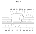
- FIG. 3 is a cross-sectional view of FIG. 1 taken along the line III-III.
- the display device includes an insulation substrate 110 that is formed of a material such as glass or plastic, and a roof layer 360,which also may by called a cover layer, formed on the insulation substrate 110.
- Microcavities 305 covered by the roof layer 360 are formed on the insulation substrate 110.
- the roof layer 360 extends in a row direction, and a plurality of microcavities 305 are formed under the single roof layer 360.
- a plurality of pixels PX are positioned on the insulation substrate 110.
- the pixels PX are arranged in a matrix form that includes a plurality of pixel columns and rows.
- One pixel PX is a region that overlaps one pixel electrode 191.
- a first valley V1 is positioned along an extending direction of a gate line 121 between the adjacent pixels PX, and a second valley V2 is positioned between rows of the adjacent pixels PX.
- the microcavities 305 may be arranged in a matrix form, the first valley V1 may be positioned between the microcavities 305 adjacent in a column direction, and the second valley V2 may be positioned between the microcavities 305 adjacent in a row direction.
- the roof layer 360 is formed in the extending direction of a data line 171. In this case, an injection hole 307 is formed in the first valley V1 such that the roof layer 360 is removed and then constituent elements positioned under the roof layer 360 are exposed.
- Each roof layer 360 is formed between the adjacent second valleys V2 to be separated from the insulation substrate 110, thereby forming the microcavity 305.
- each roof layer 360 is formed in the second valley V2 to be attached to the insulation substrate 110, thereby covering the opposite sides of the microcavity 305.
- a supporting member 365 forming opposite lateral walls of the microcavity 305 may be formed in each roof layer 360 of the second valley V2 such that it may support the microcavity 305.
- the aforementioned structure of the display device according to the first exemplary embodiment may be seen as an example, and thus it may be modified in various ways.
- arrangement of the pixel PX, the first valley V1, and the second valley V2 may be modified, the roof layers 360 may be coupled to each other in the first valley V1, and each roof layer 360 may be formed to be partially separated from the substrate 110 in the second valley V2 such that the adjacent microcavities 305 are coupled to each other.
- the display device according to the first exemplary embodiment will now be described with reference to FIGS. 1 to 3 .
- a gate conductor including the gate line 121 is formed on an insulation substrate 110 that is formed of transparent glass or plastic.
- the gate line 121 includes a wide end portion for connection with a gate electrode 124 and other layers or an external driving circuit (not shown).
- the gate line 121 may be formed of an aluminum-based metal such as aluminum (Al) or an aluminum alloy, a silver-based metal such as silver (Ag) or a silver alloy, a copper-based metal such as copper (Cu) or a copper alloy, a molybdenum-based metal such as molybdenum (Mo) or a molybdenum alloy, chromium (Cr), tantalum (Ta), titanium (Ti), etc.
- the gate line 121 may have a multilayer structure including at least two conductive layers having different physical properties.
- a gate insulating layer 140 formed of a silicon nitride (SiNx) or a silicon oxide (SiOx) is formed on the gate line 121.
- the gate insulating layer 140 may have a multilayer structure in which at least two insulating layers having different physical properties are included.
- a semiconductor 154 formed of amorphous silicon or polysilicon is formed on the gate insulating layer 140.
- the semiconductor 154 may include an oxide semiconductor.
- Ohmic contacts are formed on the semiconductor 154.
- the ohmic contacts may be formed of a material such as n+ hydrogenated amorphous silicon highly doped with an n-type impurity such as phosphorus, or may be formed of a silicide.
- the ohmic contacts may be coupled in pairs to be disposed on the semiconductor 154.
- the ohmic contacts may be omitted if the semiconductor 154 is the oxide semiconductor.
- the data line 171 including a source electrode 173 and a data conductor including a drain electrode 175 are formed on the semiconductor 154 and the gate insulating layer 140.
- the data line 171 includes a wide end portion for connection with another layer or an external driving circuit (not shown).
- the data line 171 transmits a data signal and mainly extends in a vertical direction to cross the gate line 121.
- the data line 171 may include a first curved portion having a curved shape, and parts of the curved portion may meet each other in a middle region of the pixel area to form a V shape.
- a second curved portion may be further included in the middle region of the pixel area such that it is curved to form a predetermined angle with the first curved portion.
- the first curved portion of the data line 171 may be curved to form an angle of about 7° with a vertical reference line that forms an angle of 90° with a direction in which the gate line 121 extends.
- the second curved portion disposed in the intermediate region of the pixel area may be curved to form an angle of about 7° to about 15° with the first curved portion.
- the source electrode 173 is a part of the data line 171 and is disposed on the same line as the data line 171.
- the drain electrode 175 is formed to extend in parallel with the source electrode 173. Thus, the drain electrode 175 is in parallel with the part of the data line 171.
- the gate electrode 124, the source electrode 173, and the drain electrode 175 form one thin film transistor (TFT) along with the semiconductor 154, and a channel of the thin film transistor is formed in the semiconductor 154 between the source electrode 173 and the drain electrode 175.
- TFT thin film transistor
- the display device By including the source electrode 173 that is positioned on the same line as the data line 171 and the drain electrode 175 that extends in parallel with the data line 171, the display device according to the exemplary embodiment can increase a width of the thin film transistor without increasing an area taken up by the data conductor, thereby increasing the aperture ratio of the display device.
- a display device may be formed such that its source and drain electrodes 173 and 175 have different shapes.
- the data line 171 and the drain electrode 175 may be preferably formed of a refractory metal such as molybdenum, chromium, tantalum, titanium, etc., or an alloy thereof, and they may have a multilayer structure including a refractory metal layer (not shown) and a low-resistance conductive layer (not shown).
- An example of the multilayer structure may be a double layer of a chromium or molybdenum (alloy) lower layer and an aluminum (alloy) upper layer, or a triple layer of a molybdenum (alloy) lower layer, an aluminum (alloy) middle layer, and a molybdenum (alloy) upper layer.
- the data line 171 and the drain electrode 175 may be made of various metals or conductors.
- a passivation layer 180 is disposed on the data conductors 171, 173, and 175, the gate insulating layer 140, and an exposed portion of the semiconductor 154.
- the passivation layer 180 may be made of an organic insulating material, an inorganic insulating material, or the like.
- a color filter 230 is formed in each pixel area PX on the passivation layer 180.
- Each color filter 230 may display one of the primary colors such as three primary colors of red, green, and blue.
- the color filter 230 is not limited to display the three primary colors of red, green, and blue, but may display cyan, magenta, yellow, and white-based colors. Unlike those illustrated above, the color filter 230 may be elongated in the column direction along between the adjacent data lines 171.
- An organic layer 240 is disposed on the color filter 230.
- the organic layer 240 has a larger thickness than that of the passivation layer 180, and may have a smooth surface.
- the organic layer 240 may be disposed in a display area where a plurality of pixels are disposed, and may not be disposed in a peripheral area where a gate pad portion or data pad portion is formed. Alternatively, the organic layer 240 may be positioned even in the peripheral area where the gate pad portion or data pad portion is formed.
- a contact hole 184 is provided in the organic layer 240, the color filter 230, and the passivation layer 180.
- a common electrode 270 is positioned on the organic layer 240.
- the common electrode 270 may have a planar shape, and may be disposed in the display area where the plurality of pixels are disposed but not in the peripheral area where the gate pad portion or data pad portion is formed.
- the common electrode 270 is formed of a transparent conductive layer such as indium tin oxide (ITO) or indium zinc oxide (IZO).
- ITO indium tin oxide
- IZO indium zinc oxide
- the interlayer insulating layer 250 is disposed on the common electrode 270.
- the interlayer insulating layer 250 may be formed of an inorganic insulating material such as a silicon nitride (SiNx), a silicon oxide (SiOx), a silicon oxynitride (SiOxNy), etc.
- the interlayer insulating layer 250 serves to protect the color filter 230 made of the organic material and to insulate the common electrode 270 from the pixel electrode 191. That is, even if the common electrode 270 is formed to overlap the pixel electrode 191, the common electrode 270 and the pixel electrode 191 may be prevented from being short-circuited because the interlayer insulating layer 250 is formed on the common electrode 270.
- the pixel electrode 191 is disposed on the interlayer insulating layer 250.
- the pixel electrode 191 includes a curved edge that is substantially in parallel with the first and second curved portions of the data line 171.
- the pixel electrode 191 may be formed of a transparent conductive layer such as ITO or IZO.
- the pixel electrode 191 is physically and electrically coupled to the drain electrode 175 through the contact hole 184 that is formed in the organic layer 240, the color filter 230, and the passivation layer 180, and is applied with a voltage from the drain electrode 175.
- the pixel electrode 191 is applied with a data voltage from the drain electrode 175, and the common electrode 270 is applied with a predetermined reference voltage from a reference voltage applying unit that is disposed outside of the display area.
- the pixel electrode 191 and the common electrode 270 generate an electric field according to these applied voltages, and liquid crystal molecules 310 of a liquid crystal layer over the two electrodes 191 and 270 rotate in a direction parallel to a direction of the electric field.
- Polarization of light passing through the liquid crystal layer varies depending on rotation directions of the liquid crystal molecules 310 determined as described above.
- a first insulating layer 350 may be further formed on the pixel electrode 191 such that it is separated by a predetermined distance from the pixel electrode 191.
- the first insulating layer 350 may be made of an inorganic insulating material such as a silicon nitride (SiNx), a silicon oxide (SiOx), etc.
- the microcavity 305 is formed between the pixel electrode 191 and the first insulating layer 350. In other words, the microcavity 305 is enclosed by the pixel electrode 191 and the first insulating layer 350. Widths and sizes of the microcavity 305 may be variously modified depending on sizes and resolutions of the display devices.
- a first alignment layer 11 is formed on the pixel electrode 191.
- the first alignment layer 11 may be formed directly on the interlayer insulating layer 250 that is not covered by the pixel electrode 191.
- a second alignment layer 21 is formed under the first insulating layer 350 that faces the first alignment layer 11.
- the first alignment layer 11 and the second alignment layer 21 may be formed as vertical alignment layers, and may be made of an aligning material such as polyamic acid, polysiloxane, polyimide, etc.
- the first and second alignment layers 11 and 21 may be coupled to each other at an edge of the pixel as illustrated in FIG. 3 .
- the liquid crystal layer consisting of the liquid crystal molecules 310 is formed in the microcavity 305 that is positioned between the pixel electrode 191 and the lower insulating layer 350.
- a light blocking member 220 is formed in a region between the adjacent color filters 230, and particularly, the light blocking member 220 may be positioned, as illustrated in FIG. 2 , on the pixel electrode 191 and the interlayer insulating layer 250 that is not covered by the pixel electrode 191.
- the light blocking member 220 is formed on a boundary of the pixel PX and the thin film transistor to prevent light leakage.
- the light blocking member 220 is upwardly and downwardly expanded while extending along the gate line 121, and may include a horizontal light blocking member covering a region where the thin film transistor and the like are formed and a vertical light blocking member extending along the data line 171.
- the horizontal light blocking member may be formed in the first valley V1
- the vertical light blocking member may be formed in the second valley V2.
- the color filter 230 and the light blocking member 220 may overlap each other in some regions.
- the roof layer 360 is formed on the lower (first) insulating layer 350.
- the roof layer 360 may be formed of an organic material.
- the microcavity 305 is formed under the roof layer 360, and the roof layer 360 maintains a shape of the microcavity 305 because it is hardened by a hardening process.
- the roof layer 360 is formed to be spaced apart from the pixel electrode 191 while interposing the microcavity 305 therebetween.
- the roof layer 360 is formed in each pixel PX and the second valley V2 along the pixel row, but the roof layer 360 is not formed in the first valley V1. In the second valley V2, the microcavity 305 is not formed under the roof layer 360.
- a thickness of the roof layer 360 positioned in the second valley V2 may be formed to be larger than that of the roof layer 360 that is positioned in the pixel area, and the thicker region may be referred to as a support member 365.
- the microcavity 305 is formed such that its top and lateral surfaces are covered by the roof layer 360.
- opposite sides of the microcavity 305 may be supported by the supporting member 365 formed on the same layer as the roof layer 360.
- an optical member 300 is formed on a portion corresponding to the supporting member 365 formed in the second valley V2 of the roof layer 360.
- the optical member 300 is continuously formed on a top portion of the supporting member 365 along the supporting member 365 formed on the second valley V2 in a convex semicircular-pillar shape on the insulation substrate 110. An edge of the optical member 300 overlapping at least a portion of the adjacent microcavities 305.
- the optical member 300 may be formed of the same material as the roof layer 360, and formed in an upward convex shape, thereby refracting a direction of light that is incident on the insulation substrate 110 from the outside.
- a process of rubbing the alignment layer 11 and 21 in one direction is difficult due to the microcavity 305 and the roof layer 360 covering the microcavity 305.
- a photo-alignment method that aligns the alignment layers 11 and 21 using UV irradiation and the like is used.
- a lateral wall of the microcavity 305 adjacent to the second valley V2 may be formed to be inclined. Due to the inclined lateral wall of the microcavity 305, while photo-aligning, a path of irradiated UV light is changed, thus total reflection of the UV light occurs. Accordingly, alignment may not be implemented at a portion of the alignment layers 11 and 21 corresponding to the inclined lateral wall of the microcavity 305.
- the irradiated light is vertically irradiated on the lateral wall of the microcavity 305 by using the optical member 300 according to the exemplary embodiment, thereby preventing bad alignment.
- the diameter of the optical member 300 may be formed to be wider than a width of the second valley V2, and to be narrower than a sum of widths of the second valley V2 and the microcavity 305.
- the injection hole 307 is formed in the roof layer 360 to extend to and partially expose the microcavity 305.
- the first insulating layer 350 adjacent to a region where the injection hole 307 is formed may include a region that protrudes further than the roof layer 360.
- the injection hole 307 may be formed at at least one or more edges of the pixel PX and the microcavity 305 is exposed by the injection hole 307, an aligning agent or a liquid crystal material may be injected into the microcavity 305 through the injection hole 307.
- a second insulating layer 370 may be further formed on the roof layer 360.
- the second insulating layer 370 may be made of an inorganic insulating material such as a silicon nitride (SiNx), a silicon oxide (SiOx), etc.
- the second insulating layer 370 may be formed to cover the top and lateral surfaces of the roof layer 360.
- the second insulating layer 370 serves to protect the roof layer 360 that is formed of an organic material, and may be omitted if necessary.
- the second insulating layer 370 may contact, as shown in FIG. 2 , the first insulating layer 350 that protrudes further than the roof layer 360 in a region where the injection hole 307 is positioned. Further, the second insulating layer 370 may have a stepped cross-section due to a step between a region contacting the first insulating layer 350 and a region covering the roof layer 360.
- the second insulating layer 370 may be coupled to the lower insulating layer 350.
- An overcoat 390 may be formed on the second insulating layer 370 and the injection hole 307.
- the overcoat 390 is formed to cover the injection hole 307 through which the microcavity 305 is partially exposed outside. That is, the overcoat 390 may seal the microcavity 305 such that the liquid crystal molecules 310 inside the microcavity 305 are not discharged outside.
- the overcoat 390 may be made of a material that does not react with the liquid crystal molecules 310 because it contacts the liquid crystal molecules 310.
- the overcoat 390 may be made of parylene and the like.
- the overcoat 390 serves to smooth the optical member 300 with the upward convex shape.
- the overcoat 390 may be formed of a multilayer such as a double layer, a triple layer, etc.
- the double layer may be formed of two layers that are made of different materials.
- the triple layer consists of three layers, in which forming materials of adjacent layers are different from each other.
- the overcoat 390 may include a layer formed of an organic insulating material and a layer formed of an inorganic insulating material.
- polarizers may be formed on top and bottom surfaces of the display device.
- the polarizers may include a first polarizer and a second polarizer.
- the first polarizer may be attached to a bottom surface of the insulation substrate 110, and the second polarizer may be attached on top of the overcoat 390.
- FIG. 4 is a cross-sectional view illustrating a display device according to a second exemplary embodiment
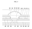
- FIG. 5 is a cross-sectional view illustrating a display device according to a third exemplary embodiment.
- an optical member 301 is continuously formed along a supporting member 365 formed in the second valley V2 in a concave semicircular shape for a direction of the insulation substrate 110.
- the optical member 301 may be formed of the same material as the roof layer 360, and may be formed in the concave semicircular shape for the direction of the insulation substrate 110, thereby refracting a direction of light that is incident on the insulation substrate 110 from the outside.
- a diameter of the optical member 301 may be formed to be wider than the width of the second valley V2, and to be narrower than the sum of widths of the second valley V2 and the microcavity 305.
- an optical member 302 may be continuously formed along the supporting member 365 formed in the second valley V2 in a upward convex shape for the insulation substrate 110, a cross-sectional surface of the optical member 302 may have a polygon shape with a many-sided surface; and a line completely linking outermost portions may have a semicircular shape.
- the optical member 302 may be formed of the same material as the roof layer 360.
- a diameter of the optical member 302 may be formed to be wider than a width of the supporting member 365 formed in the second valley V2, and to be narrower than the sum of widths of the supporting member 365 and the microcavity 305.
- FIGS. 6A and 6B are schematic diagrams for explaining an operating principle with respect to the optical member of the display device according to the first exemplary embodiment
- FIGS. 7A and 7B are schematic diagrams for explaining an operating principle with respect to the optical member of the display device according to the second exemplary embodiment.
- the lateral wall of the microcavity 305 is formed to be inclined.
- the optical members 300 and 301 according to the first and second exemplary embodiments cover the lateral walls of the adjacent microcavities 305, and are formed in an upward convex shape or a downward concave shape.
- an incident angle of light may be changed on the convex-shaped or concave-shaped optical member 300 or 301 depending on a position at which the light is incident.
- the first and second exemplary embodiments respectively, include the optical members 300 and 301, the incident angle gradually increases from a central portion to an outside portion of the semicircular shape, thus refraction of the light occurs and light may be vertically incident on the inclined lateral wall of the microcavity 305.
- one substrate may be used to manufacture the display device, thereby reducing weight, thickness, cost, and processing time of the display device, and the optical member may be included in the display device, thereby preventing total reflection of light, bad alignment, and light leakage which may occur in the display device.
- first alignment layer 21 second alignment layer 110: substrate 121: gate line 124: gate electrode 140: gate insulating layer 154: semiconductor 171: data line 173: source electrode 175: drain electrode 180: passivation layer 184: contact hole 191: pixel electrode 220: light blocking member 230: color filter 240: organic layer 250: interlayer insulating layer 270: common electrode 305: microcavity 307: injection hole 310: liquid crystal molecule 350: first insulating layer 360: roof layer 365: supporting member 370: second insulating layer 390: overcoat 300, 301, 302: optical member
Landscapes
- Physics & Mathematics (AREA)
- Nonlinear Science (AREA)
- Mathematical Physics (AREA)
- Chemical & Material Sciences (AREA)
- Crystallography & Structural Chemistry (AREA)
- General Physics & Mathematics (AREA)
- Optics & Photonics (AREA)
- Spectroscopy & Molecular Physics (AREA)
- Engineering & Computer Science (AREA)
- Microelectronics & Electronic Packaging (AREA)
- Liquid Crystal (AREA)
- Devices For Indicating Variable Information By Combining Individual Elements (AREA)
Abstract
Description
- The present application relates to a display device to be formed with one substrate and to include an optical member, and a manufacturing method thereof.
- As one of the most widely used flat panel displays at present, a liquid crystal display (LCD) includes two display panels on which electric field generating electrodes such as a pixel electrode and a common electrode are formed, and a liquid crystal layer interposed between the two display panels. The LCD generates an electric field on the liquid crystal layer by applying a voltage to the electric field generating electrodes, determines alignment directions of liquid crystal molecules of the liquid crystal layer through the generated electric field, and controls polarization of incident light, thereby displaying an image.
- Two sheets of display panels of which the LCD consists may include a thin film transistor array panel and an opposing display panel. In the thin film transistor array panel, a gate line for transmitting a gate signal and a data line for transmitting a data signal are formed to cross each other, and a thin film transistor coupled to the gate line and the data line, a pixel electrode coupled to the thin film transistor, and the like may be formed. In the opposing display panel, a light blocking member, a color filter, a common electrode, and the like may be formed. If necessary, the light blocking member, the color filter, and the common electrode may be formed on the thin film transistor array panel.
- However, in a conventional liquid crystal display, two substrates are indispensably used and constituent elements are separately formed on the two substrates, thereby requiring a long processing time as well as making the display device heavy, thick, and costly.
- The above information disclosed in this Background section is only for enhancement of understanding of the background and therefore it may contain information that does not form the prior art that is already known in this country to a person of ordinary skill in the art.
- Embodiments have been made in an effort to provide a display device and a manufacturing method thereof that may reduce weight, thickness, cost, and processing time by manufacturing the display device using one substrate.
- Further, embodiments have made in an effort to provide a display device and a manufacturing method thereof that may prevent total reflection of light, bad alignment, and light leakage by including an optical member.
- An exemplary embodiment provides a display device including: a thin film transistor disposed on an insulation substrate including a plurality of pixels; a common electrode and a pixel electrode disposed on the thin film transistor to overlap each other while interposing an insulating layer therebetween; a liquid crystal layer filling microcavities differentiated by pixel electrodes, the pixel electrodes comprising the pixel electrode; a roof layer that is disposed on a microcavity of the microcavities and includes an injection hole extending to the microcavity and a supporting member to support the microcavity; and an optical member disposed on the supporting member, wherein the injection hole is disposed between adjacent microcavities in a column direction, and the supporting member is disposed between adjacent microcavities in a row direction.
- The optical member may have a semicircular-pillar shape.
- The optical member may be disposed to have a convex shape on the insulation substrate.
- An edge of the optical member may be disposed overlapping at least a portion of adjacent microcavities.
- A diameter of the optical member may be disposed to be wider than a width of a predetermined second valley, and to be narrower than a sum of widths of the second valley and the microcavity.
- The optical member may be disposed at the same layer as the roof layer.
- Liquid crystal molecules contained in the liquid crystal layer may be disposed in a horizontal alignment mode.
- An alignment layer disposed on a surface of the microcavity may be further included, wherein the alignment layer may be a horizontal alignment layer.
- An overcoat disposed on the roof layer to cover the injection hole may be further included.
- A first insulating layer disposed under the roof layer and a second insulating layer disposed over the roof layer may be further included.
- The optical member may be disposed to have a concave shape on the insulation substrate.
- The optical member may have a many-sided surface disposed with a polygon shape, and may be disposed to have a convex shape on the insulation substrate.
- According to the exemplary embodiment, one substrate may be used to manufacture the display device, thereby reducing weight, thickness, cost, and processing time of the display device.
- In addition, according to the exemplary embodiment, the optical member may be included in the display device, thereby preventing total reflection of light, bad alignment, and light leakage which may occur in the display device.
-
-
FIG. 1 is a top plan view illustrating a pixel of a display device according to a first exemplary embodiment. -
FIG. 2 is a cross-sectional view ofFIG. 1 taken along the line II-II. -
FIG. 3 is a cross-sectional view ofFIG. 1 taken along III-III. -
FIG. 4 is a cross-sectional view illustrating a display device according to a second exemplary embodiment. -
FIG. 5 is a cross-sectional view illustrating a display device according to a third exemplary embodiment. -
FIGS. 6A and6B are schematic diagrams for explaining an operating principle with respect to an optical member of the display device according to the first exemplary embodiment. -
FIGS. 7A and7B are schematic diagrams for explaining an operating principle with respect to an optical member of the display device according to the second exemplary embodiment. - The inventive concept will be described more fully hereinafter with reference to the accompanying drawings, in which exemplary embodiments are shown. As those skilled in the art would realize, the described embodiments may be modified in various different ways, all without departing from the spirit or scope of the inventive concept.
- In the drawings, the thickness of layers, films, panels, regions, etc., are exaggerated for clarity. Like reference numerals designate like elements throughout the specification. It will be understood that when an element such as a layer, film, region, or substrate is referred to as being "on' another element, it can be directly on the other element or intervening elements may also be present. In contrast, when an element is referred to as being "directly on" another element, there are no intervening elements present.
- First, a display device according to a first exemplary embodiment will be described with reference to
FIGS. 1 to 3 . -
FIG. 1 is a top plan view illustrating a pixel of the display device according to the first exemplary embodiment,FIG. 2 is a cross-sectional view ofFIG. 1 taken along the line II-II, andFIG. 3 is a cross-sectional view ofFIG. 1 taken along the line III-III. - First, the display device according to the first exemplary embodiment will be schematically described.
- The display device according to the first exemplary embodiment includes an
insulation substrate 110 that is formed of a material such as glass or plastic, and aroof layer 360,which also may by called a cover layer, formed on theinsulation substrate 110. -
Microcavities 305 covered by theroof layer 360 are formed on theinsulation substrate 110. Theroof layer 360 extends in a row direction, and a plurality ofmicrocavities 305 are formed under thesingle roof layer 360. - A plurality of pixels PX are positioned on the
insulation substrate 110. The pixels PX are arranged in a matrix form that includes a plurality of pixel columns and rows. One pixel PX is a region that overlaps onepixel electrode 191. - A first valley V1 is positioned along an extending direction of a
gate line 121 between the adjacent pixels PX, and a second valley V2 is positioned between rows of the adjacent pixels PX. - In other words, the
microcavities 305 may be arranged in a matrix form, the first valley V1 may be positioned between themicrocavities 305 adjacent in a column direction, and the second valley V2 may be positioned between themicrocavities 305 adjacent in a row direction. - The
roof layer 360 is formed in the extending direction of adata line 171. In this case, aninjection hole 307 is formed in the first valley V1 such that theroof layer 360 is removed and then constituent elements positioned under theroof layer 360 are exposed. - Each
roof layer 360 is formed between the adjacent second valleys V2 to be separated from theinsulation substrate 110, thereby forming themicrocavity 305. In addition, eachroof layer 360 is formed in the second valley V2 to be attached to theinsulation substrate 110, thereby covering the opposite sides of themicrocavity 305. - In other words, a supporting
member 365 forming opposite lateral walls of themicrocavity 305 may be formed in eachroof layer 360 of the second valley V2 such that it may support themicrocavity 305. - The aforementioned structure of the display device according to the first exemplary embodiment may be seen as an example, and thus it may be modified in various ways. For example, arrangement of the pixel PX, the first valley V1, and the second valley V2 may be modified, the
roof layers 360 may be coupled to each other in the first valley V1, and eachroof layer 360 may be formed to be partially separated from thesubstrate 110 in the second valley V2 such that theadjacent microcavities 305 are coupled to each other. - The display device according to the first exemplary embodiment will now be described with reference to
FIGS. 1 to 3 . - First, a gate conductor including the
gate line 121 is formed on aninsulation substrate 110 that is formed of transparent glass or plastic. - The
gate line 121 includes a wide end portion for connection with agate electrode 124 and other layers or an external driving circuit (not shown). Thegate line 121 may be formed of an aluminum-based metal such as aluminum (Al) or an aluminum alloy, a silver-based metal such as silver (Ag) or a silver alloy, a copper-based metal such as copper (Cu) or a copper alloy, a molybdenum-based metal such as molybdenum (Mo) or a molybdenum alloy, chromium (Cr), tantalum (Ta), titanium (Ti), etc. However, thegate line 121 may have a multilayer structure including at least two conductive layers having different physical properties. - A
gate insulating layer 140 formed of a silicon nitride (SiNx) or a silicon oxide (SiOx) is formed on thegate line 121. Thegate insulating layer 140 may have a multilayer structure in which at least two insulating layers having different physical properties are included. - A
semiconductor 154 formed of amorphous silicon or polysilicon is formed on thegate insulating layer 140. Thesemiconductor 154 may include an oxide semiconductor. - Ohmic contacts (not shown) are formed on the
semiconductor 154. The ohmic contacts may be formed of a material such as n+ hydrogenated amorphous silicon highly doped with an n-type impurity such as phosphorus, or may be formed of a silicide. The ohmic contacts may be coupled in pairs to be disposed on thesemiconductor 154. The ohmic contacts may be omitted if thesemiconductor 154 is the oxide semiconductor. - The
data line 171 including asource electrode 173 and a data conductor including adrain electrode 175 are formed on thesemiconductor 154 and thegate insulating layer 140. - The
data line 171 includes a wide end portion for connection with another layer or an external driving circuit (not shown). Thedata line 171 transmits a data signal and mainly extends in a vertical direction to cross thegate line 121. - In this case, in order to obtain maximum transmittance of the liquid crystal display, the
data line 171 may include a first curved portion having a curved shape, and parts of the curved portion may meet each other in a middle region of the pixel area to form a V shape. A second curved portion may be further included in the middle region of the pixel area such that it is curved to form a predetermined angle with the first curved portion. - The first curved portion of the
data line 171 may be curved to form an angle of about 7° with a vertical reference line that forms an angle of 90° with a direction in which thegate line 121 extends. The second curved portion disposed in the intermediate region of the pixel area may be curved to form an angle of about 7° to about 15° with the first curved portion. - The
source electrode 173 is a part of thedata line 171 and is disposed on the same line as thedata line 171. Thedrain electrode 175 is formed to extend in parallel with thesource electrode 173. Thus, thedrain electrode 175 is in parallel with the part of thedata line 171. - The
gate electrode 124, thesource electrode 173, and thedrain electrode 175 form one thin film transistor (TFT) along with thesemiconductor 154, and a channel of the thin film transistor is formed in thesemiconductor 154 between thesource electrode 173 and thedrain electrode 175. - By including the
source electrode 173 that is positioned on the same line as thedata line 171 and thedrain electrode 175 that extends in parallel with thedata line 171, the display device according to the exemplary embodiment can increase a width of the thin film transistor without increasing an area taken up by the data conductor, thereby increasing the aperture ratio of the display device. - However, a display device according to another exemplary embodiment may be formed such that its source and drain
electrodes - The
data line 171 and thedrain electrode 175 may be preferably formed of a refractory metal such as molybdenum, chromium, tantalum, titanium, etc., or an alloy thereof, and they may have a multilayer structure including a refractory metal layer (not shown) and a low-resistance conductive layer (not shown). An example of the multilayer structure may be a double layer of a chromium or molybdenum (alloy) lower layer and an aluminum (alloy) upper layer, or a triple layer of a molybdenum (alloy) lower layer, an aluminum (alloy) middle layer, and a molybdenum (alloy) upper layer. However, in addition to those described above, thedata line 171 and thedrain electrode 175 may be made of various metals or conductors. - A
passivation layer 180 is disposed on thedata conductors gate insulating layer 140, and an exposed portion of thesemiconductor 154. Thepassivation layer 180 may be made of an organic insulating material, an inorganic insulating material, or the like. - A
color filter 230 is formed in each pixel area PX on thepassivation layer 180. Eachcolor filter 230 may display one of the primary colors such as three primary colors of red, green, and blue. Thecolor filter 230 is not limited to display the three primary colors of red, green, and blue, but may display cyan, magenta, yellow, and white-based colors. Unlike those illustrated above, thecolor filter 230 may be elongated in the column direction along between the adjacent data lines 171. - An
organic layer 240 is disposed on thecolor filter 230. Theorganic layer 240 has a larger thickness than that of thepassivation layer 180, and may have a smooth surface. - The
organic layer 240 may be disposed in a display area where a plurality of pixels are disposed, and may not be disposed in a peripheral area where a gate pad portion or data pad portion is formed. Alternatively, theorganic layer 240 may be positioned even in the peripheral area where the gate pad portion or data pad portion is formed. - A
contact hole 184 is provided in theorganic layer 240, thecolor filter 230, and thepassivation layer 180. - A
common electrode 270 is positioned on theorganic layer 240. Thecommon electrode 270 may have a planar shape, and may be disposed in the display area where the plurality of pixels are disposed but not in the peripheral area where the gate pad portion or data pad portion is formed. - The
common electrode 270 is formed of a transparent conductive layer such as indium tin oxide (ITO) or indium zinc oxide (IZO). - An interlayer insulating
layer 250 is disposed on thecommon electrode 270. The interlayer insulatinglayer 250 may be formed of an inorganic insulating material such as a silicon nitride (SiNx), a silicon oxide (SiOx), a silicon oxynitride (SiOxNy), etc. The interlayer insulatinglayer 250 serves to protect thecolor filter 230 made of the organic material and to insulate thecommon electrode 270 from thepixel electrode 191. That is, even if thecommon electrode 270 is formed to overlap thepixel electrode 191, thecommon electrode 270 and thepixel electrode 191 may be prevented from being short-circuited because theinterlayer insulating layer 250 is formed on thecommon electrode 270. - The
pixel electrode 191 is disposed on theinterlayer insulating layer 250. Thepixel electrode 191 includes a curved edge that is substantially in parallel with the first and second curved portions of thedata line 171. - The
pixel electrode 191 may be formed of a transparent conductive layer such as ITO or IZO. - The
pixel electrode 191 is physically and electrically coupled to thedrain electrode 175 through thecontact hole 184 that is formed in theorganic layer 240, thecolor filter 230, and thepassivation layer 180, and is applied with a voltage from thedrain electrode 175. - The
pixel electrode 191 is applied with a data voltage from thedrain electrode 175, and thecommon electrode 270 is applied with a predetermined reference voltage from a reference voltage applying unit that is disposed outside of the display area. - The
pixel electrode 191 and thecommon electrode 270 generate an electric field according to these applied voltages, andliquid crystal molecules 310 of a liquid crystal layer over the twoelectrodes liquid crystal molecules 310 determined as described above. - A first insulating
layer 350 may be further formed on thepixel electrode 191 such that it is separated by a predetermined distance from thepixel electrode 191. The first insulatinglayer 350 may be made of an inorganic insulating material such as a silicon nitride (SiNx), a silicon oxide (SiOx), etc. - The
microcavity 305 is formed between thepixel electrode 191 and the first insulatinglayer 350. In other words, themicrocavity 305 is enclosed by thepixel electrode 191 and the first insulatinglayer 350. Widths and sizes of themicrocavity 305 may be variously modified depending on sizes and resolutions of the display devices. - A
first alignment layer 11 is formed on thepixel electrode 191. Thefirst alignment layer 11 may be formed directly on theinterlayer insulating layer 250 that is not covered by thepixel electrode 191. - A
second alignment layer 21 is formed under the first insulatinglayer 350 that faces thefirst alignment layer 11. - The
first alignment layer 11 and thesecond alignment layer 21 may be formed as vertical alignment layers, and may be made of an aligning material such as polyamic acid, polysiloxane, polyimide, etc. The first and second alignment layers 11 and 21 may be coupled to each other at an edge of the pixel as illustrated inFIG. 3 . - The liquid crystal layer consisting of the
liquid crystal molecules 310 is formed in themicrocavity 305 that is positioned between thepixel electrode 191 and the lower insulatinglayer 350. - Further, a
light blocking member 220 is formed in a region between theadjacent color filters 230, and particularly, thelight blocking member 220 may be positioned, as illustrated inFIG. 2 , on thepixel electrode 191 and the interlayer insulatinglayer 250 that is not covered by thepixel electrode 191. Thelight blocking member 220 is formed on a boundary of the pixel PX and the thin film transistor to prevent light leakage. - The
light blocking member 220 is upwardly and downwardly expanded while extending along thegate line 121, and may include a horizontal light blocking member covering a region where the thin film transistor and the like are formed and a vertical light blocking member extending along thedata line 171. In other words, the horizontal light blocking member may be formed in the first valley V1, and the vertical light blocking member may be formed in the second valley V2. Thecolor filter 230 and thelight blocking member 220 may overlap each other in some regions. - Next, the
roof layer 360 is formed on the lower (first) insulatinglayer 350. Theroof layer 360 may be formed of an organic material. Themicrocavity 305 is formed under theroof layer 360, and theroof layer 360 maintains a shape of themicrocavity 305 because it is hardened by a hardening process. Theroof layer 360 is formed to be spaced apart from thepixel electrode 191 while interposing themicrocavity 305 therebetween. - The
roof layer 360 is formed in each pixel PX and the second valley V2 along the pixel row, but theroof layer 360 is not formed in the first valley V1. In the second valley V2, themicrocavity 305 is not formed under theroof layer 360. Thus, a thickness of theroof layer 360 positioned in the second valley V2 may be formed to be larger than that of theroof layer 360 that is positioned in the pixel area, and the thicker region may be referred to as asupport member 365. Themicrocavity 305 is formed such that its top and lateral surfaces are covered by theroof layer 360. - In other words, opposite sides of the
microcavity 305 may be supported by the supportingmember 365 formed on the same layer as theroof layer 360. - In the display device according to the first exemplary embodiment, an
optical member 300 is formed on a portion corresponding to the supportingmember 365 formed in the second valley V2 of theroof layer 360. - The
optical member 300 is continuously formed on a top portion of the supportingmember 365 along the supportingmember 365 formed on the second valley V2 in a convex semicircular-pillar shape on theinsulation substrate 110. An edge of theoptical member 300 overlapping at least a portion of theadjacent microcavities 305. - The
optical member 300 may be formed of the same material as theroof layer 360, and formed in an upward convex shape, thereby refracting a direction of light that is incident on theinsulation substrate 110 from the outside. - In a typical display device using one
insulation substrate 110, whenliquid crystal molecules 310 are not vertically aligned, that is, when theliquid crystal molecules 310 are horizontally aligned, a process of rubbing thealignment layer microcavity 305 and theroof layer 360 covering themicrocavity 305. Thus, to align the alignment layers 11 and 21 of a display device that uses oneinsulation substrate 110 and in which theliquid crystal molecules 310 are horizontally aligned, a photo-alignment method that aligns the alignment layers 11 and 21 using UV irradiation and the like is used. - When the
microcavity 305 is formed according to a typical manufacturing process of a display device, a lateral wall of themicrocavity 305 adjacent to the second valley V2 may be formed to be inclined. Due to the inclined lateral wall of themicrocavity 305, while photo-aligning, a path of irradiated UV light is changed, thus total reflection of the UV light occurs. Accordingly, alignment may not be implemented at a portion of the alignment layers 11 and 21 corresponding to the inclined lateral wall of themicrocavity 305. - Therefore, while photo-aligning, the irradiated light is vertically irradiated on the lateral wall of the
microcavity 305 by using theoptical member 300 according to the exemplary embodiment, thereby preventing bad alignment. - When a diameter of the
optical member 300 is too small or too large, the irradiated light may not be properly incident on the lateral wall of themicrocavity 305, and the path of the irradiated light may not be easily changed. Accordingly, the diameter of theoptical member 300 may be formed to be wider than a width of the second valley V2, and to be narrower than a sum of widths of the second valley V2 and themicrocavity 305. - The changing of the path of the light irradiated on the lateral wall of the
microcavity 305 by theoptical member 300 will be described later in detail. - The
injection hole 307 is formed in theroof layer 360 to extend to and partially expose themicrocavity 305. The first insulatinglayer 350 adjacent to a region where theinjection hole 307 is formed may include a region that protrudes further than theroof layer 360. - Since the
injection hole 307 may be formed at at least one or more edges of the pixel PX and themicrocavity 305 is exposed by theinjection hole 307, an aligning agent or a liquid crystal material may be injected into themicrocavity 305 through theinjection hole 307. - A second insulating
layer 370 may be further formed on theroof layer 360. The secondinsulating layer 370 may be made of an inorganic insulating material such as a silicon nitride (SiNx), a silicon oxide (SiOx), etc. The secondinsulating layer 370 may be formed to cover the top and lateral surfaces of theroof layer 360. The secondinsulating layer 370 serves to protect theroof layer 360 that is formed of an organic material, and may be omitted if necessary. - The second
insulating layer 370 may contact, as shown inFIG. 2 , the first insulatinglayer 350 that protrudes further than theroof layer 360 in a region where theinjection hole 307 is positioned. Further, the second insulatinglayer 370 may have a stepped cross-section due to a step between a region contacting the first insulatinglayer 350 and a region covering theroof layer 360. - Further, the second insulating
layer 370 may be coupled to the lower insulatinglayer 350. - An
overcoat 390 may be formed on the second insulatinglayer 370 and theinjection hole 307. - The
overcoat 390 is formed to cover theinjection hole 307 through which themicrocavity 305 is partially exposed outside. That is, theovercoat 390 may seal themicrocavity 305 such that theliquid crystal molecules 310 inside themicrocavity 305 are not discharged outside. Theovercoat 390 may be made of a material that does not react with theliquid crystal molecules 310 because it contacts theliquid crystal molecules 310. For example, theovercoat 390 may be made of parylene and the like. - Further, the
overcoat 390 serves to smooth theoptical member 300 with the upward convex shape. - The
overcoat 390 may be formed of a multilayer such as a double layer, a triple layer, etc. The double layer may be formed of two layers that are made of different materials. The triple layer consists of three layers, in which forming materials of adjacent layers are different from each other. For example, theovercoat 390 may include a layer formed of an organic insulating material and a layer formed of an inorganic insulating material. - Though not illustrated, polarizers may be formed on top and bottom surfaces of the display device. The polarizers may include a first polarizer and a second polarizer. The first polarizer may be attached to a bottom surface of the
insulation substrate 110, and the second polarizer may be attached on top of theovercoat 390. - Next, the display device according to the second and third exemplary embodiments will be described with reference to
FIGS. 4 and5 . -
FIG. 4 is a cross-sectional view illustrating a display device according to a second exemplary embodiment, andFIG. 5 is a cross-sectional view illustrating a display device according to a third exemplary embodiment. - First, compared with the display device of the first exemplary embodiment shown in
FIG. 3 , since the display devices of the second and third exemplary embodiments shown inFIGS. 4 and5 are the same as that of the first exemplary embodiment except for the shape of theoptical member 300, a repeated description thereof will be omitted. - First, as shown in
FIG. 4 , anoptical member 301 according to the second exemplary embodiment is continuously formed along a supportingmember 365 formed in the second valley V2 in a concave semicircular shape for a direction of theinsulation substrate 110. An edge of theoptical member 301 overlapping at least a portion of theadjacent microcavities 305. Theoptical member 301 may be formed of the same material as theroof layer 360, and may be formed in the concave semicircular shape for the direction of theinsulation substrate 110, thereby refracting a direction of light that is incident on theinsulation substrate 110 from the outside. - In this case, a diameter of the
optical member 301 may be formed to be wider than the width of the second valley V2, and to be narrower than the sum of widths of the second valley V2 and themicrocavity 305. - Next, referring to
FIG. 5 , anoptical member 302 according to the third exemplary embodiment may be continuously formed along the supportingmember 365 formed in the second valley V2 in a upward convex shape for theinsulation substrate 110, a cross-sectional surface of theoptical member 302 may have a polygon shape with a many-sided surface; and a line completely linking outermost portions may have a semicircular shape. - An edge of the
optical member 302 overlapping at least a portion of theadjacent microcavities 305. - The
optical member 302 may be formed of the same material as theroof layer 360. - In this case, a diameter of the
optical member 302 may be formed to be wider than a width of the supportingmember 365 formed in the second valley V2, and to be narrower than the sum of widths of the supportingmember 365 and themicrocavity 305. - An operating principle with respect to the
optical members FIGS. 6A to 7B . -
FIGS. 6A and6B are schematic diagrams for explaining an operating principle with respect to the optical member of the display device according to the first exemplary embodiment, andFIGS. 7A and7B are schematic diagrams for explaining an operating principle with respect to the optical member of the display device according to the second exemplary embodiment. - Referring to
FIGS. 6A and7A , the lateral wall of themicrocavity 305 is formed to be inclined. Theoptical members adjacent microcavities 305, and are formed in an upward convex shape or a downward concave shape. - Next, referring to
FIGS. 6B and7B , an incident angle of light may be changed on the convex-shaped or concave-shapedoptical member optical members microcavity 305. - Accordingly, while aligning the alignment layers 11 and 21, a non-aligned portion does not occur by the
optical members - According to the exemplary embodiment, one substrate may be used to manufacture the display device, thereby reducing weight, thickness, cost, and processing time of the display device, and the optical member may be included in the display device, thereby preventing total reflection of light, bad alignment, and light leakage which may occur in the display device.
- While the inventive concept has been described in connection with what is presently considered to be practical exemplary embodiments, it is to be understood that the inventive concept is not limited to the disclosed embodiments, but, on the contrary, is intended to cover various modifications and equivalent arrangements included within the spirit and scope of the appended claims.
<Description of symbols> 11: first alignment layer 21: second alignment layer 110: substrate 121: gate line 124: gate electrode 140: gate insulating layer 154: semiconductor 171: data line 173: source electrode 175: drain electrode 180: passivation layer 184: contact hole 191: pixel electrode 220: light blocking member 230: color filter 240: organic layer 250: interlayer insulating layer 270: common electrode 305: microcavity 307: injection hole 310: liquid crystal molecule 350: first insulating layer 360: roof layer 365: supporting member 370: second insulating layer 390: overcoat 300, 301, 302: optical member
Claims (11)
- A display device comprising:a thin film transistor (TFT) disposed on an insulation substrate (110) including a plurality of pixels (PX);a common electrode (270) and a pixel electrode (191) disposed on the thin film transistor (TFT) to overlap each other while interposing an insulating layer (250) therebetween;a liquid crystal layer filling microcavities (305) differentiated by pixel electrodes (191), the pixel electrodes (191) comprising the pixel electrode (191); anda roof layer (360) that is disposed on a microcavity (305) of the microcavities (305) and includes an injection hole (307) extending to the microcavity (305) and a supporting member (365) to support the microcavity (305); andan optical member (300, 301, 302) disposed on the supporting member (365),wherein the injection hole (307) is disposed between adjacent microcavities (305) in a column direction, and the supporting member (365) is disposed between adjacent microcavities (305) in a row direction.
- The display device of claim 1, wherein
the optical member (300, 301, 302) has a semicircular-pillar shape. - The display device of one of claims 1 or 2, wherein
the optical member (300, 301, 302) is disposed to have a convex shape on the insulation substrate (110). - The display device of one of claims 1 to 3, wherein
an edge of the optical member (300, 301, 302) is disposed overlapping at least a portion of adjacent microcavities (305). - The display device of one of claims 1 to 4, wherein
a diameter of the optical member (300, 301, 302) is disposed to be wider than a width of a predetermined second valley (V2), and to be narrower than a sum of widths of the second valley (V2) and the microcavity (305). - The display device of one of claims 1 to 5, wherein
the optical member (300, 301, 302) is disposed at the same layer as the roof layer (360). - The display device of one of claims 1 to 6, wherein
liquid crystal molecules (310) contained in the liquid crystal layer are disposed in a horizontal alignment mode. - The display device of one of claims 1 to 7, further comprising:an alignment layer (11,21) disposed on a surface of the microcavity (305),wherein the alignment layer (11,21) is a horizontal alignment layer (11, 21).
- The display device of one of claims 1 to 8, further comprising:an overcoat (390) disposed on the roof layer (360) to cover the injection hole (307).
- The display device of one of claims 1 to 9, further comprising:a first insulating layer (350) disposed under the roof layer (360); anda second insulating layer (370) disposed over the roof layer (360).
- The display device of one of claims 1 to 10, wherein
the optical member (300, 301, 302) is disposed to have a concave shape on the insulation substrate (110).
Applications Claiming Priority (1)
| Application Number | Priority Date | Filing Date | Title |
|---|---|---|---|
| KR1020150010087A KR20160090454A (en) | 2015-01-21 | 2015-01-21 | Display device |
Publications (1)
| Publication Number | Publication Date |
|---|---|
| EP3048474A1 true EP3048474A1 (en) | 2016-07-27 |
Family
ID=54608444
Family Applications (1)
| Application Number | Title | Priority Date | Filing Date |
|---|---|---|---|
| EP15195594.5A Withdrawn EP3048474A1 (en) | 2015-01-21 | 2015-11-20 | Display device |
Country Status (4)
| Country | Link |
|---|---|
| US (1) | US10247975B2 (en) |
| EP (1) | EP3048474A1 (en) |
| KR (1) | KR20160090454A (en) |
| CN (1) | CN105807465A (en) |
Families Citing this family (2)
| Publication number | Priority date | Publication date | Assignee | Title |
|---|---|---|---|---|
| KR102386112B1 (en) | 2015-07-30 | 2022-04-14 | 삼성디스플레이 주식회사 | Display apparatus |
| CN108957868B (en) * | 2018-07-27 | 2022-08-12 | 厦门天马微电子有限公司 | Display panel and display device |
Citations (2)
| Publication number | Priority date | Publication date | Assignee | Title |
|---|---|---|---|---|
| US20140160395A1 (en) * | 2012-12-11 | 2014-06-12 | Samsung Display Co., Ltd. | Liquid crystal display |
| EP2808729A1 (en) * | 2013-05-30 | 2014-12-03 | Samsung Display Co., Ltd. | Display device and manufacturing method thereof |
Family Cites Families (22)
| Publication number | Priority date | Publication date | Assignee | Title |
|---|---|---|---|---|
| KR20050060568A (en) | 2003-12-16 | 2005-06-22 | 엘지.필립스 엘시디 주식회사 | Transflective lcd |
| CN101341438B (en) * | 2005-12-20 | 2011-12-07 | 夏普株式会社 | Display device and liquid crystal display device |
| JP2007212969A (en) * | 2006-02-13 | 2007-08-23 | Nec Lcd Technologies Ltd | REFLECTOR, LIQUID CRYSTAL DISPLAY DEVICE PROVIDED WITH THE REFLECTOR AND MANUFACTURING METHOD THEREOF |
| TWI397745B (en) * | 2009-06-23 | 2013-06-01 | Hannstar Display Corp | Transflective dispalying device and methof for assembling the same |
| KR101613312B1 (en) | 2009-08-19 | 2016-04-20 | 삼성디스플레이 주식회사 | Display apparatus and method of manufacturing the same |
| US8351017B2 (en) * | 2009-08-26 | 2013-01-08 | Empire Technology Development, Llc | Optically intelligent image sensing device |
| KR20110046130A (en) * | 2009-10-28 | 2011-05-04 | 삼성전자주식회사 | Liquid crystal display panel |
| KR20110073210A (en) | 2009-12-21 | 2011-06-29 | 엘지디스플레이 주식회사 | Backlight unit |
| KR101605821B1 (en) | 2010-09-10 | 2016-03-24 | 삼성디스플레이 주식회사 | Display device and fabrication method thereof |
| US8614776B2 (en) | 2010-10-26 | 2013-12-24 | Samsung Display Co., Ltd. | Display panel, display apparatus having the same, method of manufacturing the same and method of cutting the same |
| KR101844015B1 (en) * | 2011-02-24 | 2018-04-02 | 삼성디스플레이 주식회사 | Liquid crystal display |
| KR101822078B1 (en) | 2011-06-14 | 2018-01-26 | 삼성디스플레이 주식회사 | Display panel and manufacturing method thereof |
| KR101887217B1 (en) | 2012-01-06 | 2018-08-10 | 삼성디스플레이 주식회사 | Display apparatus and method of manufacturing the same |
| KR101697703B1 (en) | 2012-01-18 | 2017-01-19 | 삼성디스플레이 주식회사 | Display apparatus and method of manufacturing the same |
| KR20130121545A (en) * | 2012-04-27 | 2013-11-06 | 삼성디스플레이 주식회사 | Display device and manufacturing method thereof |
| KR101984873B1 (en) * | 2012-05-07 | 2019-06-03 | 삼성디스플레이 주식회사 | Display device and manufacturing method thereof |
| KR101665558B1 (en) | 2012-11-23 | 2016-10-25 | 삼성디스플레이 주식회사 | Liquid crystal display device and manufacturing method thereof |
| KR20150007175A (en) * | 2013-07-10 | 2015-01-20 | 삼성디스플레이 주식회사 | Display device and manufacturing method thereof |
| KR20150008758A (en) | 2013-07-15 | 2015-01-23 | 삼성디스플레이 주식회사 | Liquid crystal display device and manufacturing method thereof |
| KR102057970B1 (en) | 2013-08-01 | 2019-12-23 | 삼성디스플레이 주식회사 | Display device and manufacturing method thereof |
| KR102106004B1 (en) | 2013-10-22 | 2020-05-04 | 삼성디스플레이 주식회사 | Liquid crystal display and method of manufacturing the same |
| KR20150055952A (en) | 2013-11-14 | 2015-05-22 | 삼성디스플레이 주식회사 | Liquid crystal display and method of manufacturing the same |
-
2015
- 2015-01-21 KR KR1020150010087A patent/KR20160090454A/en not_active Ceased
- 2015-11-13 US US14/941,393 patent/US10247975B2/en active Active
- 2015-11-17 CN CN201510792644.3A patent/CN105807465A/en active Pending
- 2015-11-20 EP EP15195594.5A patent/EP3048474A1/en not_active Withdrawn
Patent Citations (2)
| Publication number | Priority date | Publication date | Assignee | Title |
|---|---|---|---|---|
| US20140160395A1 (en) * | 2012-12-11 | 2014-06-12 | Samsung Display Co., Ltd. | Liquid crystal display |
| EP2808729A1 (en) * | 2013-05-30 | 2014-12-03 | Samsung Display Co., Ltd. | Display device and manufacturing method thereof |
Also Published As
| Publication number | Publication date |
|---|---|
| KR20160090454A (en) | 2016-08-01 |
| US20160209699A1 (en) | 2016-07-21 |
| CN105807465A (en) | 2016-07-27 |
| US10247975B2 (en) | 2019-04-02 |
Similar Documents
| Publication | Publication Date | Title |
|---|---|---|
| US10663813B2 (en) | Liquid crystal display | |
| US9658482B2 (en) | Liquid crystal display | |
| EP2752879B1 (en) | Thin film transistor array panel | |
| US9291849B2 (en) | Liquid crystal display | |
| KR102334140B1 (en) | Display device and manufacturing method thereof | |
| US9366897B2 (en) | Display device and manufacturing method thereof | |
| US9530364B2 (en) | Liquid crystal display | |
| KR20120004045A (en) | Liquid crystal display | |
| US9568798B2 (en) | Liquid crystal display | |
| US10168584B2 (en) | Liquid crystal display having improved texture resistance and side visibility | |
| US9829759B2 (en) | Liquid crystal display device | |
| US20160124275A1 (en) | Liquid crystal display having improved transmittance | |
| US8017947B2 (en) | Thin film transistor array panel, display device including the same, and method thereof | |
| US9625769B2 (en) | Liquid crystal display including protruding auxiliary wires corresponding to spacer | |
| KR102262431B1 (en) | Liquid crystal display | |
| US10247975B2 (en) | Display device | |
| US10162238B2 (en) | Display device | |
| US20170102591A1 (en) | Liquid crystal display device | |
| US9897842B2 (en) | Display device and manufacturing method thereof | |
| KR20060092521A (en) | Liquid crystal display |
Legal Events
| Date | Code | Title | Description |
|---|---|---|---|
| PUAI | Public reference made under article 153(3) epc to a published international application that has entered the european phase |
Free format text: ORIGINAL CODE: 0009012 |
|
| AK | Designated contracting states |
Kind code of ref document: A1 Designated state(s): AL AT BE BG CH CY CZ DE DK EE ES FI FR GB GR HR HU IE IS IT LI LT LU LV MC MK MT NL NO PL PT RO RS SE SI SK SM TR |
|
| AX | Request for extension of the european patent |
Extension state: BA ME |
|
| 17P | Request for examination filed |
Effective date: 20160923 |
|
| RBV | Designated contracting states (corrected) |
Designated state(s): AL AT BE BG CH CY CZ DE DK EE ES FI FR GB GR HR HU IE IS IT LI LT LU LV MC MK MT NL NO PL PT RO RS SE SI SK SM TR |
|
| GRAP | Despatch of communication of intention to grant a patent |
Free format text: ORIGINAL CODE: EPIDOSNIGR1 |
|
| RIC1 | Information provided on ipc code assigned before grant |
Ipc: G02F 1/1337 20060101ALI20180822BHEP Ipc: G02F 1/1335 20060101ALI20180822BHEP Ipc: G02F 1/1333 20060101AFI20180822BHEP |
|
| INTG | Intention to grant announced |
Effective date: 20180912 |
|
| STAA | Information on the status of an ep patent application or granted ep patent |
Free format text: STATUS: THE APPLICATION IS DEEMED TO BE WITHDRAWN |
|
| 18D | Application deemed to be withdrawn |
Effective date: 20190123 |