EP3043266A1 - Store merge processing device, store merge processing system, store merge processing method, and storage medium - Google Patents
Store merge processing device, store merge processing system, store merge processing method, and storage medium Download PDFInfo
- Publication number
- EP3043266A1 EP3043266A1 EP14842063.1A EP14842063A EP3043266A1 EP 3043266 A1 EP3043266 A1 EP 3043266A1 EP 14842063 A EP14842063 A EP 14842063A EP 3043266 A1 EP3043266 A1 EP 3043266A1
- Authority
- EP
- European Patent Office
- Prior art keywords
- entry
- information
- storage
- address
- block
- Prior art date
- Legal status (The legal status is an assumption and is not a legal conclusion. Google has not performed a legal analysis and makes no representation as to the accuracy of the status listed.)
- Ceased
Links
Images





Classifications
-
- G—PHYSICS
- G06—COMPUTING OR CALCULATING; COUNTING
- G06F—ELECTRIC DIGITAL DATA PROCESSING
- G06F12/00—Accessing, addressing or allocating within memory systems or architectures
- G06F12/02—Addressing or allocation; Relocation
- G06F12/08—Addressing or allocation; Relocation in hierarchically structured memory systems, e.g. virtual memory systems
- G06F12/12—Replacement control
- G06F12/121—Replacement control using replacement algorithms
-
- G—PHYSICS
- G06—COMPUTING OR CALCULATING; COUNTING
- G06F—ELECTRIC DIGITAL DATA PROCESSING
- G06F3/00—Input arrangements for transferring data to be processed into a form capable of being handled by the computer; Output arrangements for transferring data from processing unit to output unit, e.g. interface arrangements
- G06F3/06—Digital input from, or digital output to, record carriers, e.g. RAID, emulated record carriers or networked record carriers
- G06F3/0601—Interfaces specially adapted for storage systems
- G06F3/0602—Interfaces specially adapted for storage systems specifically adapted to achieve a particular effect
- G06F3/061—Improving I/O performance
- G06F3/0611—Improving I/O performance in relation to response time
-
- G—PHYSICS
- G06—COMPUTING OR CALCULATING; COUNTING
- G06F—ELECTRIC DIGITAL DATA PROCESSING
- G06F12/00—Accessing, addressing or allocating within memory systems or architectures
- G06F12/02—Addressing or allocation; Relocation
- G06F12/08—Addressing or allocation; Relocation in hierarchically structured memory systems, e.g. virtual memory systems
- G06F12/10—Address translation
- G06F12/1027—Address translation using associative or pseudo-associative address translation means, e.g. translation look-aside buffer [TLB]
- G06F12/1036—Address translation using associative or pseudo-associative address translation means, e.g. translation look-aside buffer [TLB] for multiple virtual address spaces, e.g. segmentation
-
- G—PHYSICS
- G06—COMPUTING OR CALCULATING; COUNTING
- G06F—ELECTRIC DIGITAL DATA PROCESSING
- G06F12/00—Accessing, addressing or allocating within memory systems or architectures
- G06F12/02—Addressing or allocation; Relocation
- G06F12/08—Addressing or allocation; Relocation in hierarchically structured memory systems, e.g. virtual memory systems
- G06F12/12—Replacement control
- G06F12/121—Replacement control using replacement algorithms
- G06F12/128—Replacement control using replacement algorithms adapted to multidimensional cache systems, e.g. set-associative, multicache, multiset or multilevel
-
- G—PHYSICS
- G06—COMPUTING OR CALCULATING; COUNTING
- G06F—ELECTRIC DIGITAL DATA PROCESSING
- G06F3/00—Input arrangements for transferring data to be processed into a form capable of being handled by the computer; Output arrangements for transferring data from processing unit to output unit, e.g. interface arrangements
- G06F3/06—Digital input from, or digital output to, record carriers, e.g. RAID, emulated record carriers or networked record carriers
- G06F3/0601—Interfaces specially adapted for storage systems
- G06F3/0628—Interfaces specially adapted for storage systems making use of a particular technique
- G06F3/0638—Organizing or formatting or addressing of data
- G06F3/064—Management of blocks
-
- G—PHYSICS
- G06—COMPUTING OR CALCULATING; COUNTING
- G06F—ELECTRIC DIGITAL DATA PROCESSING
- G06F3/00—Input arrangements for transferring data to be processed into a form capable of being handled by the computer; Output arrangements for transferring data from processing unit to output unit, e.g. interface arrangements
- G06F3/06—Digital input from, or digital output to, record carriers, e.g. RAID, emulated record carriers or networked record carriers
- G06F3/0601—Interfaces specially adapted for storage systems
- G06F3/0668—Interfaces specially adapted for storage systems adopting a particular infrastructure
- G06F3/0671—In-line storage system
- G06F3/0673—Single storage device
- G06F3/0679—Non-volatile semiconductor memory device, e.g. flash memory, one time programmable memory [OTP]
-
- G—PHYSICS
- G06—COMPUTING OR CALCULATING; COUNTING
- G06F—ELECTRIC DIGITAL DATA PROCESSING
- G06F2212/00—Indexing scheme relating to accessing, addressing or allocation within memory systems or architectures
- G06F2212/62—Details of cache specific to multiprocessor cache arrangements
- G06F2212/621—Coherency control relating to peripheral accessing, e.g. from DMA or I/O device
-
- G—PHYSICS
- G06—COMPUTING OR CALCULATING; COUNTING
- G06F—ELECTRIC DIGITAL DATA PROCESSING
- G06F2212/00—Indexing scheme relating to accessing, addressing or allocation within memory systems or architectures
- G06F2212/65—Details of virtual memory and virtual address translation
- G06F2212/657—Virtual address space management
Definitions
- the claimed invention relates to a store merge processing device and the like that, after collecting a plurality of write instructions of which access addresses are within a predetermined region, issues the write instructions to the storage device of a writing target.
- Store merge processing is known as processing when the access addresses relating to a plurality of write instructions are, for example, on the same line for performing writing to a storage device, such as a main memory or a cache.
- a write instruction is not transmitted to a storage device one by one, but a write instruction is transmitted to the storage device after write instructions are collected as one instruction.
- Store merge processing can improve the performance of accessing a storage device by decreasing the number of write accesses to the storage device.
- PTL 1 discloses a device that includes a store buffer which stores data relating to a plurality of write instructions and suppresses access to a storage device, even when write instructions for different addresses on the storage device are issued.
- PTL 2 discloses a device that realizes a decreased number of partial write accesses for the main memory by having a plurality of address buffers and data buffers in parallel for storing addresses and data relating to partial write processing for the main memory.
- PTL 3 discloses a system of performing store merge processing by merging write data using a data queue for temporarily storing write data, in the same way as byte marks.
- store merge processing is performed except in the case of a combination of a leading full write access and a subsequent partial write access.
- PTLs 1 and 2 do not particularly refer to a technique of performing store merge processing, when there are accesses with different block sizes relating to write data.
- PTLs 3 refers to store merge processing when there are accesses with different block sizes relating to write data, but PTL 3 is not sufficient to solve the above-described problem, as there are significant limitations for performing store merge processing.
- the main objective of the claimed invention is to realize store merge processing with simple hardware even when there are accesses with different block sizes relating to write data for a storage device.
- An aspect of the present invention is a store merge processing device including: a storage means that stores a plurality of entries, with regard to a plurality of first write instructions that are a plurality of write instructions issued by an external device issuable of write instructions of different block sizes, have access addresses including upper addresses and lower addresses, of which upper addresses are equal and have equal block sizes for writing data to a storage device, the entries including identification information for identifying a block size, a plurality of pieces of block data, address information indicating an upper address, and storage information indicating a storage state for each piece of the block data in association with one another; and an update means for, when the entries include an entry of which identification information and address information matches those of a second write instruction that has been newly issued by the external device, writing the block data included in the second write instruction in a position specified by the access address in the entry, and updates the storage information regarding the block data.
- a store merge processing method including: by an information processing device, storing, with regard to a plurality of first write instructions that are a plurality of write instructions issued by an external device issuable of write instructions of different block sizes, have access addresses including upper addresses and lower addresses, of which upper addresses are equal, and have equal block sizes for writing data to a storage device, into any one of a plurality of entries, identification information for identifying a block size, a plurality of pieces of block data, address information indicating an upper address, and storage information indicating a storage state for each piece of the block data in association with one another; and when the entries include an entry of which identification information and address information match those of a second write instruction that has been newly issued by the external device, writing the block data included in the second write instruction in a position specified by the access address in the entry, and updating the storage information regarding the block data.
- a storage medium that stores a store merge program causing a computer to execute: storage processing that stores, with regard to a plurality of first write instructions that are a plurality of write instructions issued by an external device issuable of write instructions of different block sizes, have access addresses including upper addresses and lower addresses, of which upper addresses are equal, and have equal block sizes for writing data to a storage device, into any one of a plurality of entries, identification information for identifying a block size, a plurality of pieces of block data, address information indicating an upper address, and storage information indicating a storage state for each piece of the block data in association with one another; and update processing that, when the entries include an entry, of which identification information and address information match those of a second write instruction that has been newly issued by the external device, writes the block data included in the second write instruction in a position specified by the access address in the entry, and updates the storage information regarding the block data.
- the present invention can be implemented by a non-transitory computer readable storage medium storing the above information reading program (computer program).
- the claimed invention enables implementation of store merge processing with simple hardware even when there are accesses with different block sizes relating to write data for a storage device.
- Fig. 1 is a block diagram conceptually illustrating a configuration of a store merge processing system 1 in a first exemplary embodiment.
- the store merge processing system 1 in the first exemplary embodiment has a store merge processing device 10, a central processing unit 20, and a main memory 30.
- the central processing unit 20 issues a write instruction 200 for the main memory 20, and transmits the write instruction 200, together with write data 210, to the store merge processing device 10.
- the bus width of an input/output interface relating to the central processing unit 20 is 8 bytes (hereinafter, bytes are expressed as B), and the write data 210 is assumed to be 8B data.
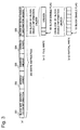
- the write instruction 200 includes block size identification information 201, an address (upper) 202, an address (middle) 203, an address (lower) 204, and block-by-block enable information 205.
- the block size identification information 201 is information for identifying the block size of the write data 210 relating to the write instruction 200.
- the block size identification information 201 is set to "1" for a full write instruction of 4B block size, and "0" for a partial write instruction of 1B block size by the central processing unit 20.
- the address (upper) 202, the address (middle) 203, and the address (lower) 204 are the access address in the main memory 30 relating to the write instruction 200, and are, respectively, upper bits, middle bits, and lower bits of the access address.
- the block-by-block enable information 205 is 8-bit information that indicates whether or not each piece of block data in the write data 210 is valid. As illustrated in (b-1) of Fig. 3 , when the write instruction 200 is a full write instruction, the block-by-block enable information 205 indicates whether or not each of two pieces of 4B data included in the write data 210 is valid. In this case, the remaining 6 bits in the block-by-block enable information are unused. As illustrated in (b-2) of Fig. 3 , when the write instruction 200 is a partial write instruction, the block-by-block enable information 205 indicates whether or not each of eight pieces of 1B data included in the write data 210 is valid.
- the store merge processing device 10 performs store merge processing, when store merge processing can be performed with respect to the received plurality of the write instructions 200 and the write data 210. After this processing, the store merge processing device 10 transmits a write instruction as a collection of the plurality of write instructions to the main memory 30.
- the main memory 30 writes data to the designated address in accordance with the write instruction received from the store merge processing device 10. It is assumed that the line size for accessing the main memory 30 is 128B.
- the store merge processing device 10 includes a storage unit 11, an update unit 12, and a generation unit 13.
- the storage unit 11 is a storage device, such as an electronic memory, of which access is controlled by an electronic circuit or a computer program and a processor that operates in accordance with the computer program.
- the update unit 12 and the generation unit 13 may be an electronic circuit, or realized by a computer program and a processor that operates in accordance with the computer program.
- the storage unit 11 includes a store buffer address array 110 and a store buffer data array 111.
- the store buffer address array 110 stores a plurality of entries that include information which serves as a basis for the update unit 12 to determine whether or not store merge processing is possible for writing to a specific address of the main memory 30.
- the store buffer data array 111 holds write data for the main memory 30, that is associated with each entry in the store buffer address array 110.
- Each entry in the store buffer data array 111 stores 128B data with respect to a full write instruction, and 32B data with respect to a partial write instruction as write data equal to one line of the main memory 30.
- One entry in the store buffer address array 110 and the store buffer data array 111 includes information relating to one specific address, and the entry is registered and updated by the update unit 12.
- Each entry includes valid information 1101, block size identification information 1102, address information 1103, and block data storage information 1104 in association with one another.
- the valid information 1101 is information that indicates whether or not the relevant entry is valid, and the valid information is set to "1" when the relevant entry is valid and "0" when the relevant entry is invalid or unused.
- the block size identification information 1102 is information that indicates whether the relevant entry is an entry relating to access data of a full write instruction or an entry relating to access data of a partial write instruction. The block size identification information 1102 is set to "0" for the former case and "1" for the latter case.
- the address information 1103 is information relating to an access address for the main memory 30.
- the block data storage information 1104 is 32-bit information that indicates, for each block data in the write data, whether store merge processing relating to the relevant entry is performed as write data for the main memory 30.
- the block data storage information 1104 includes 32 flags. Each flag in the block data storage information 1104 indicates information on each 4B block with respect to a full write instruction, and information on each 1B block with respect to a partial write instruction.
- Fig. 5 also illustrates how information included in a write instruction 200 is used, when the update unit 12 updates an entry in the store buffer address array 110 and the store buffer data array 111.
- the store buffer address array 110 and the store buffer data array 111 store information by m ways of a set associative method that includes m (m is integer not less than 1) number of entries for each address, of which address (middle) 203 in the main memory 30 is equal.
- Each entry in the store buffer address array 110 holds a value indicated by the address (upper) 202 as address information 1103.
- the update unit 12 receives the write instruction 200 and the write data 210 for the main memory 30 that were issued by the central processing unit 20.
- the search circuit 120 in the update unit 12 searches a predetermined entry from among m number of entries designated by the address (middle) 203 in the store buffer address array 110.
- the predetermined entry is an entry, of which address information 1103 is equal to the address (upper) 202, and valid information 1101 is "1".
- the search circuit 120 inputs the search result to a selection circuit 121 in the update unit 12.
- the update unit 12 When the block size identification information 1102 in the entry, that is searched and specified by the search circuit 120, is equal to the block size identification information 201 in the write instruction 200, the update unit 12 performs the following processing: That is, the update unit 12 specifies the position of block data from values indicated by the block size identification information 201 and the address (lower) 204 with respect to the block data, of which block-by-block enable information 205 with respect to the block data is set to "1". The update unit 12 sets the flag with respect to the relevant block data in the block data storage information 1104 to "1".
- the selection circuit 121 selects an entry that is associated with the above-described entry in the store buffer data array 111 based on the search result which is input from the search circuit 120.
- the update unit 12 writes the block data that is specified by values indicated by the block size identification information 201, the address (lower) 204, and the block-by-block enable information 205 to the entry selected by the selection circuit 121 as store buffer data 1110.
- the search circuit 120 checks whether there is an unused entry, of which valid information 1101 is "0" from the m number of entries. When there is at least one unused entry, the search circuit 120 selects any one of the unused entries and inputs the selection result to the selection circuit 121.
- the update unit 12 sets the valid information 1101 in the relevant entry to "1", sets the block size identification information 1102 to the value indicated by the block size identification information 201, and sets the address information 1103 to the value indicated by the address (upper) 202.
- the selection circuit 121 selects an entry that is associated with the above-described entry in the store buffer data array 111 based on the selection result which is input by the search circuit 120.
- the update unit 12 writes the block data that is specified by values indicated by the block size identification information 201, the address (lower) 204, and the block-by-block enable information 205 to the entry selected by the selection circuit 121 as the store buffer data 1110.
- the search circuit 120 selects any one of entries from among the m number of entries in accordance with predetermined criteria.
- the predetermined criteria include an algorithm, such as LRU (Least Recently Used).
- the search circuit 120 inputs the selection result to the selection circuit 121.
- the selection circuit 121 selects an entry that is associated with the above-described entry in the store buffer data array 111 based on the selection result which is input from the search circuit 120.
- the update unit 12 inputs information that is held in the entry in the store buffer address array 110 selected by the search circuit 120, and in the entry in the store buffer data array 111 selected by the selection circuit 121 to the generation unit 13.
- the update unit 12 sets the values relating to the block size identification information 1102, the address information 1103, and the block data storage information 1104 to the entry selected by the search circuit 120 in the same way as described above. Further, the update unit 12 writes the block data in the entry selected by the selection circuit 121 as store buffer data 1110.
- the update unit 12 inputs the information held in the entry selected by the search circuit 120 and selection circuit 121 to the generation unit 13.
- the update unit 12 in the same way as described above, inputs the values to the entry selected by the search circuit 120 and selection circuit 121.
- the generation unit 13 Based on the information input by the update unit 12, the generation unit 13 generates a write instruction for the main memory 30 and transmits the generated write instruction to the main memory 30, together with the write data.
- the generation unit 13 generates a write instruction, as illustrated in a write instruction list 130 generated by the generation unit 13 for the main memory 30, based on the values indicated by the block size identification information 1102 and the block data storage information 1104.
- the generation unit 13 For example, in the case 1 where the block size identification information 1102 indicates full write and 32 bits relating to the block data storage information 1104 are all "1", the generation unit 13 generates a 128B write instruction once. In the case 5 where the block size identification information 1102 indicates partial write and 32 bits relating to the block data storage information 1104 are all "1", the generation unit 13 generates a 32B write instruction once.
- the case 1 and the case 5 are illustrated in Fig. 7A .
- the generation unit 13 In the case 2 where the block size identification information 1102 indicates full write and the upper half or the lower half of 16 bits relating to the block data storage information 1104 are all "1" (exclusive of a case corresponding to the case 1), the generation unit 13 generates a 64B write instruction once. In the case 6 where the block size identification information 1102 indicates partial write and the upper half or the lower half of 16 bits relating to the block data storage information 1104 are all "1" (exclusive of a case corresponding to the case 5), the generation unit 13 generates a 16B write instruction once. An example of the case 2 and the case 6 is illustrated in Fig. 7B .
- the generation unit 13 When the block data storage information 1104 is the value illustrated in Fig. 7C , incase that the block size identification information 1102 indicates full write, the generation unit 13 generates a 4B write instruction for seven times and a 32B write instruction once. When the block size identification information 1102 indicates partial write, the generation unit 13 generates a 1B write instruction for seven times and a 32B write instruction once.
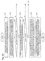
- the update unit 12 receives the write instruction 200 and write data 210 for the main memory 30, that are issued by the central processing unit 20 (step S101).
- the update unit 12 searches an entry, of which address information 1103 is equal to the address (upper) 202 and the valid information 1101 is "1" from among the m number of entries, which are designated by the address (middle) 203, in the store buffer address array 110 (step S102).
- the update unit 12 compares the block size identification information 1102 in the hit entry and the block size identification information 201 (step S104). When the values are equal (Yes at step S105), the update unit 12 sets a flag, specified by the block size identification information 201, the address (lower) 204, and the block-by-block enable information 205 in the block data storage information 1104 of the relevant entry, to "1" (step S106). The update unit 12 writes block data specified by the block size identification information 201, the address (lower) 204, and the block-by-block enable information 205 in an entry relating to the relevant entry in the store buffer data array 111 (step S107). This ends the entire processing.
- the update unit 12 checks whether there is an unused entry, of which valid information 1101 is "0", from among the m number of entries designated by the address (middle) 203, in the store buffer address array 110 (step S201). When there are unused entries (Yes at step S202), the update unit 12 selects any one of the unused entries and sets the valid information in the relevant entry to "1", the block size identification information 1102 to the value indicated by the block size identification information 201, and the address information 1103 to the value indicated by the address (upper) 202 (S203). The processing thereafter proceeds to step S106.
- the update unit 12 selects any one of the entries from the m number of entries designated by the address (middle) 203 in the store buffer address array 110 in accordance with predetermined criteria (step S301).
- the update unit 12 inputs the information held in the selected entry and the entry in the store buffer data array 111, which is associated with the relevant entry, to the generation unit 13 (step S302).
- the generation unit 13 generates a write instruction for the main memory 30 based on the input information, and transmits the generated write instruction to the main memory 30 together with the write data (step S303).
- the update unit 12 sets the block size identification information 1102 in the relevant entry to the value indicated by the block size identification information 201, and the address information 1103 to the value indicated by the address (upper) 202 (step S304), and the processing proceeds to step S106.
- step S105 When the values are different at step S105 (No at step S105), the update unit 12 inputs the information held in the hit entry and the entry in the store buffer data array 111, which is associated with the relevant entry, to the generation unit 13 (step S305). The processing thereafter proceeds to step S303.
- the store merge processing device 10 can realize store merge processing by simple hardware even when there are accesses with different block sizes relating to write data for a storage device. This is because of the following reasons: that is,
- each entry in the storage unit 11 stores block size identification information 1102.
- the update unit 12 performs store merge processing, when there is an entry relating to a write instruction with equal block size and access address to the received write instruction 200. That is, the store merge processing device 10 performs store merge processing after confirming that the data of equal block size is written in the same address region.
- the store merge processing device 10 can realize store merge processing by simple hardware even in a system where there are accesses with different block sizes relating to write data for a storage device.
- the generation unit 13 in the first exemplary embodiment generates a write instruction for collectively writing a plurality of pieces of block data to the main memory 30. Accordingly, the store merge processing device 10 can improve the performance of accessing the main memory 30 by decreasing the number of write accesses for the main memory 30.
- the target, to which the store merge processing device 10 writes data is not limited to the main memory, and may be, for example, a storage device, such as a cache.
- the central processing unit 30 issues a write instruction of two kinds of block sizes, full write accesses and partial write accesses, but the central processing unit 30 may issue a write instruction of three or more kinds of block sizes.
- the block size identification information 1102 in each entry indicates a value that identifies three or more kinds of block sizes, and the store merge processing device 10 performs store merge processing for writing data of equal block sizes in the same address region.
- Fig. 8 is a block diagram conceptually illustrating a configuration of the store merge processing device 40 in a second exemplary embodiment.
- the store merge processing device 40 in the second exemplary embodiment includes a storage unit 41 and an update unit 42.
- the storage unit 41 receives a plurality of write instructions issued by an external device 50 issuable of write instructions with different block sizes.
- the storage unit 41 includes n (n is integer of 2 or more) number of entries 410-1 to 410-n. Each of the entries 410-1 to 410-n has an access address within a predetermined region, and stores predetermined information with respect to a plurality of write instructions with equal block sizes for writing data to the storage device 60.
- the predetermined information includes identification information for identifying a block size, a plurality of pieces of block data, address information indicating the position of a predetermined region, and storage information indicating the storage state of each piece of block data, that are stored in association with one another.
- the update unit 42 stores the block data included in the relevant write instruction in a position specified by the access address in the relevant entry. Along with that, the update unit 42 updates the storage information relating to the relevant block data.
- the second exemplary embodiment can realize store merge processing with simple hardware, even when there are accesses with different block sizes relating to write data for a storage device. This is because of the following reason: each entry in the storage unit 41 stores identification information for identifying a block size. Further, the update unit 42 performs store merge processing relating to the received write instruction based on the information stored in the entry relating to the write instruction, of which block size and access address are equal to the received write instruction.
- each part illustrated in Figs. 1 and 8 can be regarded as functional (processing) units (software modules) of a software program.
- processing processing units
- categorization of each part illustrated in the drawings is a configuration for convenience of explanation, and various configurations may be considered for implementation.
- An example of the hardware environment in such a case will be described with reference to Fig. 9 .
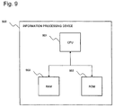
- Fig. 9 is a diagram illustratively describing a configuration of the information processing device 900 (a computer) that can execute the store merge processing device according to the exemplary embodiments of the present invention. That is, Fig. 9 is a computer (information processing device) configuration that can realize store merge processing device illustrated in Figs. 1 and 8 , which represents hardware environment that can realize each function of the above-described exemplary embodiments.
- the information processing device 900 illustrated in Fig. 9 is a common computer including a CPU 901 (Central Processing Unit), a ROM 902 (Read Only Memory), and a RAM 903 (Random Access Memory), all of which components are connected to one another through a bus (a communication line).
- a CPU 901 Central Processing Unit
- ROM 902 Read Only Memory
- RAM 903 Random Access Memory
- the present invention described with the above-described exemplary embodiments as examples provides the information processing device 900 illustrated in Fig. 9 with a computer program that can realize the functions of the block configuration diagrams ( Figs. 1 and 8 ) or the flowcharts ( Figs. 2A to 2C ), which are referred to in the description of the exemplary embodiments.
- the functions are achieved by loading the computer program on the CPU 901 of the relevant hardware, interpreting and executing the computer program.
- the computer program provided in the relevant device may be stored in a storage device, such as a readable and writable volatile storage memory (RAM 903) or non-volatile storage memory (ROM 902).
- the present invention is described using the above-described exemplary embodiments as typical examples. However, the present invention is not limited to the above-described exemplary embodiments. That is, the present invention can be applied to a variety of modes that can be understood by those skilled in the art within the scope of the present invention.
Landscapes
- Engineering & Computer Science (AREA)
- Theoretical Computer Science (AREA)
- Physics & Mathematics (AREA)
- General Engineering & Computer Science (AREA)
- General Physics & Mathematics (AREA)
- Human Computer Interaction (AREA)
- Memory System Of A Hierarchy Structure (AREA)
- Memory System (AREA)
Abstract
Description
- The claimed invention relates to a store merge processing device and the like that, after collecting a plurality of write instructions of which access addresses are within a predetermined region, issues the write instructions to the storage device of a writing target.
- Store merge processing is known as processing when the access addresses relating to a plurality of write instructions are, for example, on the same line for performing writing to a storage device, such as a main memory or a cache. In store merge processing, a write instruction is not transmitted to a storage device one by one, but a write instruction is transmitted to the storage device after write instructions are collected as one instruction. Store merge processing can improve the performance of accessing a storage device by decreasing the number of write accesses to the storage device.
- A technique relating to such store merge processing is, for example, disclosed in
PTL 1.PTL 1 discloses a device that includes a store buffer which stores data relating to a plurality of write instructions and suppresses access to a storage device, even when write instructions for different addresses on the storage device are issued. - Further,
PTL 2 discloses a device that realizes a decreased number of partial write accesses for the main memory by having a plurality of address buffers and data buffers in parallel for storing addresses and data relating to partial write processing for the main memory. - Further,
PTL 3 discloses a system of performing store merge processing by merging write data using a data queue for temporarily storing write data, in the same way as byte marks. In this system, store merge processing is performed except in the case of a combination of a leading full write access and a subsequent partial write access. -
- [PTL 1] Japanese Unexamined Patent Application Publication No.
2012-043202 - [PTL 2] Japanese Unexamined Patent Application Publication No. Hei
09-282221 - [PTL 3] Japanese Unexamined Patent Application Publication No.
Hei 05-181742 - In write accesses to a storage device, such as a main memory or a cache, there are cases where there are accesses with different sizes of block data that constitute write data, such as full write accesses and partial write accesses. When store merge processing is performed in a system where there are such cases, it is necessary to consider that the units for collecting write data are matched, and there is a problem that it is difficult to realize store merge processing with a simple hardware configuration.
- The above-described
PTLs - Further,
PTLs 3 refers to store merge processing when there are accesses with different block sizes relating to write data, butPTL 3 is not sufficient to solve the above-described problem, as there are significant limitations for performing store merge processing. - The main objective of the claimed invention is to realize store merge processing with simple hardware even when there are accesses with different block sizes relating to write data for a storage device.
- An aspect of the present invention is a store merge processing device including: a storage means that stores a plurality of entries, with regard to a plurality of first write instructions that are a plurality of write instructions issued by an external device issuable of write instructions of different block sizes, have access addresses including upper addresses and lower addresses, of which upper addresses are equal and have equal block sizes for writing data to a storage device, the entries including identification information for identifying a block size, a plurality of pieces of block data, address information indicating an upper address, and storage information indicating a storage state for each piece of the block data in association with one another; and an update means for, when the entries include an entry of which identification information and address information matches those of a second write instruction that has been newly issued by the external device, writing the block data included in the second write instruction in a position specified by the access address in the entry, and updates the storage information regarding the block data.
- Another aspect of the present invention, to achieve the above object, is a store merge processing method including: by an information processing device, storing, with regard to a plurality of first write instructions that are a plurality of write instructions issued by an external device issuable of write instructions of different block sizes, have access addresses including upper addresses and lower addresses, of which upper addresses are equal, and have equal block sizes for writing data to a storage device, into any one of a plurality of entries, identification information for identifying a block size, a plurality of pieces of block data, address information indicating an upper address, and storage information indicating a storage state for each piece of the block data in association with one another; and when the entries include an entry of which identification information and address information match those of a second write instruction that has been newly issued by the external device, writing the block data included in the second write instruction in a position specified by the access address in the entry, and updating the storage information regarding the block data.
- Another aspect of the present invention, to achieve the above object, is a storage medium that stores a store merge program causing a computer to execute: storage processing that stores, with regard to a plurality of first write instructions that are a plurality of write instructions issued by an external device issuable of write instructions of different block sizes, have access addresses including upper addresses and lower addresses, of which upper addresses are equal, and have equal block sizes for writing data to a storage device, into any one of a plurality of entries, identification information for identifying a block size, a plurality of pieces of block data, address information indicating an upper address, and storage information indicating a storage state for each piece of the block data in association with one another; and update processing that, when the entries include an entry, of which identification information and address information match those of a second write instruction that has been newly issued by the external device, writes the block data included in the second write instruction in a position specified by the access address in the entry, and updates the storage information regarding the block data.
- Furthermore, the present invention can be implemented by a non-transitory computer readable storage medium storing the above information reading program (computer program).
- The claimed invention enables implementation of store merge processing with simple hardware even when there are accesses with different block sizes relating to write data for a storage device.
-
-
Fig. 1 is a block diagram illustrating a configuration of a store merge processing system according to a first exemplary embodiment of the claimed invention; -
Fig. 2A is a flowchart (1 of 3) illustrating operation of the store merge processing system in the first exemplary embodiment of the claimed invention; -
Fig. 2B is a flowchart (2 of 3) illustrating operation of the store merge processing system in the first exemplary embodiment of the claimed invention; -
Fig. 2C is a flowchart (3 of 3) illustrating operation of the store merge processing system in the first exemplary embodiment of the claimed invention; -
Fig. 3 is a diagram illustrating a configuration example of a write instruction for the main memory, that is issued from the central processing unit, in the first exemplary embodiment of the claimed invention; -
Fig. 4 is a diagram illustrating a configuration example of information, that is stored in each entry of the store buffer address array, in the first exemplary embodiment of the claimed invention; -
Fig. 5 is a block diagram illustrating a detailed configuration of an update unit in the first exemplary embodiment of the claimed invention; -
Fig. 6 is a diagram illustrating a list of write instructions for the main memory, that is generated by a generation unit, in the first exemplary embodiment of the claimed invention; -
Fig. 7A is a diagram (1 of 3) illustrating a specific example relating to a write instruction for the main memory, that is generated by the generation unit, in the first exemplary embodiment of the claimed invention; -
Fig. 7B is a diagram (2 of 3) illustrating a specific example relating to a write instruction for the main memory, that is generated by the generation unit, in the first exemplary embodiment of the claimed invention; -
Fig. 7C is a diagram (3 of 3) illustrating a specific example relating to a write instruction for the main memory, that is generated by the generation unit, in the first exemplary embodiment of the claimed invention; -
Fig. 8 is a block diagram illustrating a configuration of a store merge processing device according to a second exemplary embodiment of the claimed invention; and -
Fig. 9 is a block diagram illustrating a configuration of an information processing device that can execute a store merge processing device, in the exemplary embodiments of the claimed invention. - The following will describe the details of the exemplary embodiments of the claimed invention with reference to the drawings.
-
Fig. 1 is a block diagram conceptually illustrating a configuration of a storemerge processing system 1 in a first exemplary embodiment. The storemerge processing system 1 in the first exemplary embodiment has a storemerge processing device 10, acentral processing unit 20, and amain memory 30. - The
central processing unit 20 issues awrite instruction 200 for themain memory 20, and transmits thewrite instruction 200, together with writedata 210, to the storemerge processing device 10. The bus width of an input/output interface relating to thecentral processing unit 20 is 8 bytes (hereinafter, bytes are expressed as B), and thewrite data 210 is assumed to be 8B data. - A configuration example of the
write instruction 200 is illustrated inFig. 3 . Thewrite instruction 200, as illustrated in (a) ofFig. 3 , includes blocksize identification information 201, an address (upper) 202, an address (middle) 203, an address (lower) 204, and block-by-block enableinformation 205. - The block
size identification information 201 is information for identifying the block size of the writedata 210 relating to thewrite instruction 200. The blocksize identification information 201 is set to "1" for a full write instruction of 4B block size, and "0" for a partial write instruction of 1B block size by thecentral processing unit 20. The address (upper) 202, the address (middle) 203, and the address (lower) 204 are the access address in themain memory 30 relating to thewrite instruction 200, and are, respectively, upper bits, middle bits, and lower bits of the access address. - The block-by-block enable
information 205 is 8-bit information that indicates whether or not each piece of block data in thewrite data 210 is valid. As illustrated in (b-1) ofFig. 3 , when thewrite instruction 200 is a full write instruction, the block-by-block enableinformation 205 indicates whether or not each of two pieces of 4B data included in thewrite data 210 is valid. In this case, the remaining 6 bits in the block-by-block enable information are unused. As illustrated in (b-2) ofFig. 3 , when thewrite instruction 200 is a partial write instruction, the block-by-block enableinformation 205 indicates whether or not each of eight pieces of 1B data included in thewrite data 210 is valid. - The store
merge processing device 10 performs store merge processing, when store merge processing can be performed with respect to the received plurality of thewrite instructions 200 and thewrite data 210. After this processing, the storemerge processing device 10 transmits a write instruction as a collection of the plurality of write instructions to themain memory 30. - The
main memory 30 writes data to the designated address in accordance with the write instruction received from the storemerge processing device 10. It is assumed that the line size for accessing themain memory 30 is 128B. - The store
merge processing device 10 includes astorage unit 11, anupdate unit 12, and ageneration unit 13. Thestorage unit 11 is a storage device, such as an electronic memory, of which access is controlled by an electronic circuit or a computer program and a processor that operates in accordance with the computer program. Theupdate unit 12 and thegeneration unit 13 may be an electronic circuit, or realized by a computer program and a processor that operates in accordance with the computer program. - The
storage unit 11 includes a storebuffer address array 110 and a storebuffer data array 111. The storebuffer address array 110 stores a plurality of entries that include information which serves as a basis for theupdate unit 12 to determine whether or not store merge processing is possible for writing to a specific address of themain memory 30. The storebuffer data array 111 holds write data for themain memory 30, that is associated with each entry in the storebuffer address array 110. Each entry in the storebuffer data array 111stores 128B data with respect to a full write instruction, and 32B data with respect to a partial write instruction as write data equal to one line of themain memory 30. One entry in the storebuffer address array 110 and the storebuffer data array 111 includes information relating to one specific address, and the entry is registered and updated by theupdate unit 12. - A configuration example of information held in each entry of the store
buffer address array 110 is illustrated inFig. 4 . Each entry includesvalid information 1101, blocksize identification information 1102,address information 1103, and blockdata storage information 1104 in association with one another. Thevalid information 1101 is information that indicates whether or not the relevant entry is valid, and the valid information is set to "1" when the relevant entry is valid and "0" when the relevant entry is invalid or unused. The blocksize identification information 1102 is information that indicates whether the relevant entry is an entry relating to access data of a full write instruction or an entry relating to access data of a partial write instruction. The blocksize identification information 1102 is set to "0" for the former case and "1" for the latter case. - The
address information 1103 is information relating to an access address for themain memory 30. The blockdata storage information 1104 is 32-bit information that indicates, for each block data in the write data, whether store merge processing relating to the relevant entry is performed as write data for themain memory 30. The blockdata storage information 1104 includes 32 flags. Each flag in the blockdata storage information 1104 indicates information on each 4B block with respect to a full write instruction, and information on each 1B block with respect to a partial write instruction. - The detailed configuration of the
update unit 12 is illustrated inFig. 5. Fig. 5 also illustrates how information included in awrite instruction 200 is used, when theupdate unit 12 updates an entry in the storebuffer address array 110 and the storebuffer data array 111. - As illustrated in
Fig. 5 , the storebuffer address array 110 and the storebuffer data array 111 store information by m ways of a set associative method that includes m (m is integer not less than 1) number of entries for each address, of which address (middle) 203 in themain memory 30 is equal. Each entry in the storebuffer address array 110 holds a value indicated by the address (upper) 202 asaddress information 1103. - The
update unit 12 receives thewrite instruction 200 and thewrite data 210 for themain memory 30 that were issued by thecentral processing unit 20. Thesearch circuit 120 in theupdate unit 12 searches a predetermined entry from among m number of entries designated by the address (middle) 203 in the storebuffer address array 110. The predetermined entry is an entry, of which addressinformation 1103 is equal to the address (upper) 202, andvalid information 1101 is "1". Thesearch circuit 120 inputs the search result to aselection circuit 121 in theupdate unit 12. - When the block
size identification information 1102 in the entry, that is searched and specified by thesearch circuit 120, is equal to the blocksize identification information 201 in thewrite instruction 200, theupdate unit 12 performs the following processing: That is, theupdate unit 12 specifies the position of block data from values indicated by the blocksize identification information 201 and the address (lower) 204 with respect to the block data, of which block-by-block enableinformation 205 with respect to the block data is set to "1". Theupdate unit 12 sets the flag with respect to the relevant block data in the blockdata storage information 1104 to "1". Theselection circuit 121 selects an entry that is associated with the above-described entry in the storebuffer data array 111 based on the search result which is input from thesearch circuit 120. Theupdate unit 12 writes the block data that is specified by values indicated by the blocksize identification information 201, the address (lower) 204, and the block-by-block enableinformation 205 to the entry selected by theselection circuit 121 asstore buffer data 1110. - There is a case where there is no entry, of which address
information 1103 is equal to the address (upper) 202, andvalid information 1101 is "1" in the above-described m number of entries. In such a case, thesearch circuit 120 checks whether there is an unused entry, of whichvalid information 1101 is "0" from the m number of entries. When there is at least one unused entry, thesearch circuit 120 selects any one of the unused entries and inputs the selection result to theselection circuit 121. Theupdate unit 12 sets thevalid information 1101 in the relevant entry to "1", sets the blocksize identification information 1102 to the value indicated by the blocksize identification information 201, and sets theaddress information 1103 to the value indicated by the address (upper) 202. Theselection circuit 121 selects an entry that is associated with the above-described entry in the storebuffer data array 111 based on the selection result which is input by thesearch circuit 120. Theupdate unit 12 writes the block data that is specified by values indicated by the blocksize identification information 201, the address (lower) 204, and the block-by-block enableinformation 205 to the entry selected by theselection circuit 121 as thestore buffer data 1110. - When there is no unused entry in the m number of entries as the result of the above-described checking of whether there is an unused entry, the
search circuit 120 selects any one of entries from among the m number of entries in accordance with predetermined criteria. The predetermined criteria include an algorithm, such as LRU (Least Recently Used). Thesearch circuit 120 inputs the selection result to theselection circuit 121. Theselection circuit 121 selects an entry that is associated with the above-described entry in the storebuffer data array 111 based on the selection result which is input from thesearch circuit 120. Theupdate unit 12 inputs information that is held in the entry in the storebuffer address array 110 selected by thesearch circuit 120, and in the entry in the storebuffer data array 111 selected by theselection circuit 121 to thegeneration unit 13. Theupdate unit 12 sets the values relating to the blocksize identification information 1102, theaddress information 1103, and the blockdata storage information 1104 to the entry selected by thesearch circuit 120 in the same way as described above. Further, theupdate unit 12 writes the block data in the entry selected by theselection circuit 121 asstore buffer data 1110. - Suppose there is an entry, of which address
information 1103 searched and specified by thesearch circuit 120 is equal to the address (upper) 202, and thevalid information 1101 is "1". Further, with respect to this entry, suppose the value indicated by the blocksize identification information 1102 is different from the value indicated by the blocksize identification information 201 in thewrite instruction 200. In this case, in the same way as described above, theupdate unit 12 inputs the information held in the entry selected by thesearch circuit 120 andselection circuit 121 to thegeneration unit 13. Theupdate unit 12, in the same way as described above, inputs the values to the entry selected by thesearch circuit 120 andselection circuit 121. - Based on the information input by the
update unit 12, thegeneration unit 13 generates a write instruction for themain memory 30 and transmits the generated write instruction to themain memory 30, together with the write data. - An example of the write instruction for the
main memory 30, generated by thegeneration unit 13, is illustrated inFigs. 6 to 7C . Thegeneration unit 13 generates a write instruction, as illustrated in awrite instruction list 130 generated by thegeneration unit 13 for themain memory 30, based on the values indicated by the blocksize identification information 1102 and the blockdata storage information 1104. - For example, in the
case 1 where the blocksize identification information 1102 indicates full write and 32 bits relating to the blockdata storage information 1104 are all "1", thegeneration unit 13 generates a 128B write instruction once. In thecase 5 where the blocksize identification information 1102 indicates partial write and 32 bits relating to the blockdata storage information 1104 are all "1", thegeneration unit 13 generates a 32B write instruction once. Thecase 1 and thecase 5 are illustrated inFig. 7A . - In the
case 2 where the blocksize identification information 1102 indicates full write and the upper half or the lower half of 16 bits relating to the blockdata storage information 1104 are all "1" (exclusive of a case corresponding to the case 1), thegeneration unit 13 generates a 64B write instruction once. In thecase 6 where the blocksize identification information 1102 indicates partial write and the upper half or the lower half of 16 bits relating to the blockdata storage information 1104 are all "1" (exclusive of a case corresponding to the case 5), thegeneration unit 13 generates a 16B write instruction once. An example of thecase 2 and thecase 6 is illustrated inFig. 7B . - When the block
data storage information 1104 is the value illustrated inFig. 7C , incase that the blocksize identification information 1102 indicates full write, thegeneration unit 13 generates a 4B write instruction for seven times and a 32B write instruction once. When the blocksize identification information 1102 indicates partial write, thegeneration unit 13 generates a 1B write instruction for seven times and a 32B write instruction once. - Next, operation (processing) of the store
merge processing system 1 in the first exemplary embodiment will be described in detail with reference to the flowchart ofFigs. 2A to 2C . - The
update unit 12 receives thewrite instruction 200 and writedata 210 for themain memory 30, that are issued by the central processing unit 20 (step S101). Theupdate unit 12 searches an entry, of which addressinformation 1103 is equal to the address (upper) 202 and thevalid information 1101 is "1" from among the m number of entries, which are designated by the address (middle) 203, in the store buffer address array 110 (step S102). - When any one of the entries is hit (Yes at step S103), the
update unit 12 compares the blocksize identification information 1102 in the hit entry and the block size identification information 201 (step S104). When the values are equal (Yes at step S105), theupdate unit 12 sets a flag, specified by the blocksize identification information 201, the address (lower) 204, and the block-by-block enableinformation 205 in the blockdata storage information 1104 of the relevant entry, to "1" (step S106). Theupdate unit 12 writes block data specified by the blocksize identification information 201, the address (lower) 204, and the block-by-block enableinformation 205 in an entry relating to the relevant entry in the store buffer data array 111 (step S107). This ends the entire processing. - When there is no hit entry at step S103 (No at step S103), the
update unit 12 checks whether there is an unused entry, of whichvalid information 1101 is "0", from among the m number of entries designated by the address (middle) 203, in the store buffer address array 110 (step S201). When there are unused entries (Yes at step S202), theupdate unit 12 selects any one of the unused entries and sets the valid information in the relevant entry to "1", the blocksize identification information 1102 to the value indicated by the blocksize identification information 201, and theaddress information 1103 to the value indicated by the address (upper) 202 (S203). The processing thereafter proceeds to step S106. - When there is no unused entry at step S202 (No at step S202), the
update unit 12 selects any one of the entries from the m number of entries designated by the address (middle) 203 in the storebuffer address array 110 in accordance with predetermined criteria (step S301). Theupdate unit 12 inputs the information held in the selected entry and the entry in the storebuffer data array 111, which is associated with the relevant entry, to the generation unit 13 (step S302). - The
generation unit 13 generates a write instruction for themain memory 30 based on the input information, and transmits the generated write instruction to themain memory 30 together with the write data (step S303). Theupdate unit 12 sets the blocksize identification information 1102 in the relevant entry to the value indicated by the blocksize identification information 201, and theaddress information 1103 to the value indicated by the address (upper) 202 (step S304), and the processing proceeds to step S106. - When the values are different at step S105 (No at step S105), the
update unit 12 inputs the information held in the hit entry and the entry in the storebuffer data array 111, which is associated with the relevant entry, to the generation unit 13 (step S305). The processing thereafter proceeds to step S303. - The store
merge processing device 10 according to the first exemplary embodiment can realize store merge processing by simple hardware even when there are accesses with different block sizes relating to write data for a storage device. This is because of the following reasons: that is, - Each entry in the
storage unit 11 stores the blocksize identification information 1102. - The
update unit 12 performs store merge processing relating to thewrite instruction 200 based on the information stored in the entries relating to the write instructions, of which block sizes and access addresses are equal to those of the receivedwrite instruction 200. - In a system where there are accesses with different block sizes relating to write data for the storage device, there are cases where data of different block sizes are written in the same address region. Even in such cases, there is a problem that the size of hardware, which performs store merge processing, becomes larger as data of different block sizes are merged when store merge processing is performed.
- In the store
merge processing device 10 in the first exemplary embodiment, each entry in thestorage unit 11 stores blocksize identification information 1102. Theupdate unit 12 performs store merge processing, when there is an entry relating to a write instruction with equal block size and access address to the receivedwrite instruction 200. That is, the storemerge processing device 10 performs store merge processing after confirming that the data of equal block size is written in the same address region. Thus, it is not necessary to have a function of merging data of different block sizes. Accordingly, the storemerge processing device 10 can realize store merge processing by simple hardware even in a system where there are accesses with different block sizes relating to write data for a storage device. - Further, when the block
data storage information 1104 input by theupdate unit 12 indicates that a plurality of pieces of block data with continuous access addresses are in a state of store merge processing, thegeneration unit 13 in the first exemplary embodiment generates a write instruction for collectively writing a plurality of pieces of block data to themain memory 30. Accordingly, the storemerge processing device 10 can improve the performance of accessing themain memory 30 by decreasing the number of write accesses for themain memory 30. - Note that the target, to which the store
merge processing device 10 writes data, is not limited to the main memory, and may be, for example, a storage device, such as a cache. - Further, in the exemplary embodiment, the
central processing unit 30 issues a write instruction of two kinds of block sizes, full write accesses and partial write accesses, but thecentral processing unit 30 may issue a write instruction of three or more kinds of block sizes. In such a case, the blocksize identification information 1102 in each entry indicates a value that identifies three or more kinds of block sizes, and the storemerge processing device 10 performs store merge processing for writing data of equal block sizes in the same address region. -
Fig. 8 is a block diagram conceptually illustrating a configuration of the storemerge processing device 40 in a second exemplary embodiment. - The store
merge processing device 40 in the second exemplary embodiment includes astorage unit 41 and anupdate unit 42. - The
storage unit 41 receives a plurality of write instructions issued by anexternal device 50 issuable of write instructions with different block sizes. Thestorage unit 41 includes n (n is integer of 2 or more) number of entries 410-1 to 410-n. Each of the entries 410-1 to 410-n has an access address within a predetermined region, and stores predetermined information with respect to a plurality of write instructions with equal block sizes for writing data to thestorage device 60. The predetermined information includes identification information for identifying a block size, a plurality of pieces of block data, address information indicating the position of a predetermined region, and storage information indicating the storage state of each piece of block data, that are stored in association with one another. - There are cases where there are entries for a write instruction, of which identification information for identifying the block size matches, and a predetermined region specified by the address information includes an access address. In this case, the
update unit 42 stores the block data included in the relevant write instruction in a position specified by the access address in the relevant entry. Along with that, theupdate unit 42 updates the storage information relating to the relevant block data. - The second exemplary embodiment can realize store merge processing with simple hardware, even when there are accesses with different block sizes relating to write data for a storage device. This is because of the following reason: each entry in the
storage unit 41 stores identification information for identifying a block size. Further, theupdate unit 42 performs store merge processing relating to the received write instruction based on the information stored in the entry relating to the write instruction, of which block size and access address are equal to the received write instruction. - In each of the above-described exemplary embodiments, each part illustrated in
Figs. 1 and8 can be regarded as functional (processing) units (software modules) of a software program. However, the categorization of each part illustrated in the drawings is a configuration for convenience of explanation, and various configurations may be considered for implementation. An example of the hardware environment in such a case will be described with reference toFig. 9 . -
Fig. 9 is a diagram illustratively describing a configuration of the information processing device 900 (a computer) that can execute the store merge processing device according to the exemplary embodiments of the present invention. That is,Fig. 9 is a computer (information processing device) configuration that can realize store merge processing device illustrated inFigs. 1 and8 , which represents hardware environment that can realize each function of the above-described exemplary embodiments. - The
information processing device 900 illustrated inFig. 9 is a common computer including a CPU 901 (Central Processing Unit), a ROM 902 (Read Only Memory), and a RAM 903 (Random Access Memory), all of which components are connected to one another through a bus (a communication line). - Then, the present invention described with the above-described exemplary embodiments as examples provides the
information processing device 900 illustrated inFig. 9 with a computer program that can realize the functions of the block configuration diagrams (Figs. 1 and8 ) or the flowcharts (Figs. 2A to 2C ), which are referred to in the description of the exemplary embodiments. Hereafter, the functions are achieved by loading the computer program on theCPU 901 of the relevant hardware, interpreting and executing the computer program. Further, the computer program provided in the relevant device may be stored in a storage device, such as a readable and writable volatile storage memory (RAM 903) or non-volatile storage memory (ROM 902). - As above, the present invention is described using the above-described exemplary embodiments as typical examples. However, the present invention is not limited to the above-described exemplary embodiments. That is, the present invention can be applied to a variety of modes that can be understood by those skilled in the art within the scope of the present invention.
- This application claims priority based on Japanese Patent Application No.
2013-183215 filed on September 4, 2013 -
- 1 Store merge processing system
- 10 Store merge processing device
- 11 Storage unit
- 110 Store buffer address array
- 111 Store buffer data array
- 1101 Valid information
- 1102 Block size identification information
- 1103 Address information
- 1104 Block data storage information
- 1110 Store buffer data
- 12 Update unit
- 120 Search circuit
- 121 Selection circuit
- 13 Generation unit
- 130 Write instruction list for
main memory 30, generated bygeneration unit 13 - 20 Central processing unit
- 200 Write instruction
- 201 Block size identification information
- 202 Address (upper)
- 203 Address (middle)
- 204 Address (lower)
- 205 Block-by-block enable information
- 30 Main memory
- 40 Store merge processing device
- 41 Storage unit
- 410-1 to 410-n Entry
- 42 Update unit
- 50 External device
- 60 Storage device
- 900 Information processing device
- 901 CPU
- 902 ROM
- 903 RAM
Claims (10)
- A store merge processing device comprising:a storage means that stores a plurality of entries, with regard to a plurality of first write instructions that are a plurality of write instructions issued by an external device issuable of write instructions of different block sizes, have access addresses including upper addresses and lower addresses, of which upper addresses are equal and have equal block sizes for writing data to a storage device, the entries including identification information for identifying a block size, a plurality of pieces of block data, address information indicating an upper address, and storage information indicating a storage state for each piece of the block data in association with one another; andan update means for, when the entries include an entry of which identification information and address information matches those of a second write instruction that has been newly issued by the external device, writing the block data included in the second write instruction in a position specified by the access address in the entry, and updates the storage information regarding the block data.
- The store merge processing device according to Claim 1, further comprising:a generation means for, when the storage information stored in the entry indicates that the entry stores a plurality of pieces of block data with continuous access addresses, generating a write instruction for collectively writing a plurality of pieces of block data to the storage device based on the identification information, address information, and storage information stored in the entry.
- The store merge processing device according to Claim 2, wherein
the update means, when there is no entry, of which identification information and address information match those of the second write instruction, and there is no unused entry, selects any one of the entries in accordance with a predetermined criteria, and inputs the identification information, block data, address information, and storage information stored in the selected entry to the generation means; and
the generation means generates a write instruction for writing into the storage device, based on the identification information, block data, address information, and storage information that was input from the update means. - A store merge processing system comprising: the store merge processing device according to any one of Claims 1 to 3 and the storage device.
- A store merge processing method comprising:by an information processing device,storing, with regard to a plurality of first write instructions that are a plurality of write instructions issued by an external device issuable of write instructions of different block sizes, have access addresses including upper addresses and lower addresses, of which upper addresses are equal, and have equal block sizes for writing data to a storage device, into any one of a plurality of entries, identification information for identifying a block size, a plurality of pieces of block data, address information indicating an upper address, and storage information indicating a storage state for each piece of the block data in association with one another; andwhen the entries include an entry of which identification information and address information match those of a second write instruction that has been newly issued by the external device, writing the block data included in the second write instruction in a position specified by the access address in the entry, and updating the storage information regarding the block data.
- The store merge processing method according to Claim 5, comprising:by an information processing device,when the storage information stored in the entry indicates that the entry stores a plurality of pieces of block data with continuous access addresses, generating a write instruction for collectively writing a plurality of pieces of block data to the storage device based on the identification information, address information, and storage information stored in the entry.
- The store merge processing method according to Claim 6, comprising:by an information processing device,when there is no entry, of which identification information and address information match those of the second write instruction, and there is no unused entry, selecting any one of the entries in accordance with a predetermined criteria; andgenerating a write instruction for writing into the storage device, based on the identification information, block data, address information, and storage information that is stored in the selected entry.
- A storage medium that stores a store merge program causing a computer to execute:storage processing that stores, with regard to a plurality of first write instructions that are a plurality of write instructions issued by an external device issuable of write instructions of different block sizes, have access addresses including upper addresses and lower addresses, of which upper addresses are equal, and have equal block sizes for writing data to a storage device, into any one of a plurality of entries, identification information for identifying a block size, a plurality of pieces of block data, address information indicating an upper address, and storage information indicating a storage state for each piece of the block data in association with one another; andupdate processing that, when the entries include an entry, of which identification information and address information match those of a second write instruction that has been newly issued by the external device, writes the block data included in the second write instruction in a position specified by the access address in the entry, and updates the storage information regarding the block data.
- The storage medium that stores the store merge program according to Claim 8 causing a computer to execute:when the storage information stored in the entry indicates that the entry stores a plurality of pieces of block data with continuous access addresses, generation processing that generates a write instruction for collectively writing a plurality of pieces of block data to the storage device based on the identification information, address information, and storage information stored in the entry.
- The storage medium that stores the store merge program according to Claim 9 for causing a computer to execute:when there is no entry, of which identification information and address information match those of the second write instruction, and there is no unused entry, selecting any one of the entries in accordance with a predetermined criteria, inputting the identification information, block data, address information, and storage information stored in the selected entry to the generation processing; andthe generation processing that generates a write instruction for writing into the storage device, based on the identification information, block data, address information, and storage information that is input from the update processing.
Applications Claiming Priority (2)
| Application Number | Priority Date | Filing Date | Title |
|---|---|---|---|
| JP2013183215A JP5658336B1 (en) | 2013-09-04 | 2013-09-04 | Store merge processing device, store merge processing system, store merge processing method, and store merge processing program |
| PCT/JP2014/004493 WO2015033551A1 (en) | 2013-09-04 | 2014-09-02 | Store merge processing device, store merge processing system, store merge processing method, and recording medium |
Publications (2)
| Publication Number | Publication Date |
|---|---|
| EP3043266A1 true EP3043266A1 (en) | 2016-07-13 |
| EP3043266A4 EP3043266A4 (en) | 2017-04-19 |
Family
ID=52437449
Family Applications (1)
| Application Number | Title | Priority Date | Filing Date |
|---|---|---|---|
| EP14842063.1A Ceased EP3043266A4 (en) | 2013-09-04 | 2014-09-02 | Store merge processing device, store merge processing system, store merge processing method, and storage medium |
Country Status (4)
| Country | Link |
|---|---|
| US (1) | US20160217082A1 (en) |
| EP (1) | EP3043266A4 (en) |
| JP (1) | JP5658336B1 (en) |
| WO (1) | WO2015033551A1 (en) |
Cited By (1)
| Publication number | Priority date | Publication date | Assignee | Title |
|---|---|---|---|---|
| EP3392762A4 (en) * | 2015-12-14 | 2019-08-07 | NEC Platforms, Ltd. | STORAGE / FUSION DEVICE, INFORMATION PROCESSING DEVICE, STORAGE CONTROL METHOD, AND RECORDING MEDIUM FOR RECORDING A COMPUTER PROGRAM |
Families Citing this family (5)
| Publication number | Priority date | Publication date | Assignee | Title |
|---|---|---|---|---|
| US9686191B2 (en) * | 2015-08-21 | 2017-06-20 | KnuEdge Incorporation | Performing read operations in network on a chip architecture |
| CN114063882B (en) | 2020-07-31 | 2024-09-03 | 伊姆西Ip控股有限责任公司 | Method, electronic device and computer program product for storage management |
| CN113486018B (en) * | 2021-07-23 | 2023-09-26 | 北京京东振世信息技术有限公司 | Production data storage method, storage device, electronic equipment and storage medium |
| US12236096B2 (en) * | 2021-10-22 | 2025-02-25 | EMC IP Holding Company, LLC | System and method for aggregation of write commits to control written block size |
| CN117742793B (en) * | 2023-11-01 | 2024-07-02 | 上海合芯数字科技有限公司 | Instruction merging circuit, method and chip for data cache instructions |
Family Cites Families (9)
| Publication number | Priority date | Publication date | Assignee | Title |
|---|---|---|---|---|
| JP3263110B2 (en) * | 1992-01-08 | 2002-03-04 | 富士通株式会社 | Store merge control method |
| JPH09282221A (en) | 1996-04-19 | 1997-10-31 | Hitachi Ltd | Main memory controller |
| JP2001325147A (en) * | 2000-05-17 | 2001-11-22 | Hitachi Ltd | Partial store processing method, memory system and large scale integrated circuit |
| US8180931B2 (en) * | 2004-01-20 | 2012-05-15 | Super Talent Electronics, Inc. | USB-attached-SCSI flash-memory system with additional command, status, and control pipes to a smart-storage switch |
| TWI371691B (en) * | 2007-12-16 | 2012-09-01 | Infortrend Technology Inc | Storage controller for handling data stream and method thereof |
| TWI372974B (en) * | 2008-03-24 | 2012-09-21 | Phison Electronics Corp | Management method, management apparatus and controller for memory data access |
| US8131951B2 (en) * | 2008-05-30 | 2012-03-06 | Freescale Semiconductor, Inc. | Utilization of a store buffer for error recovery on a store allocation cache miss |
| JP5522731B2 (en) * | 2010-08-19 | 2014-06-18 | エヌイーシーコンピュータテクノ株式会社 | Store merge apparatus, information processing apparatus, store merge method and program |
| TWI447646B (en) * | 2011-11-18 | 2014-08-01 | Asmedia Technology Inc | Data transmission device and method for merging multiple instruction |
-
2013
- 2013-09-04 JP JP2013183215A patent/JP5658336B1/en not_active Expired - Fee Related
-
2014
- 2014-09-02 EP EP14842063.1A patent/EP3043266A4/en not_active Ceased
- 2014-09-02 WO PCT/JP2014/004493 patent/WO2015033551A1/en not_active Ceased
- 2014-09-02 US US14/914,138 patent/US20160217082A1/en not_active Abandoned
Cited By (1)
| Publication number | Priority date | Publication date | Assignee | Title |
|---|---|---|---|---|
| EP3392762A4 (en) * | 2015-12-14 | 2019-08-07 | NEC Platforms, Ltd. | STORAGE / FUSION DEVICE, INFORMATION PROCESSING DEVICE, STORAGE CONTROL METHOD, AND RECORDING MEDIUM FOR RECORDING A COMPUTER PROGRAM |
Also Published As
| Publication number | Publication date |
|---|---|
| WO2015033551A1 (en) | 2015-03-12 |
| JP5658336B1 (en) | 2015-01-21 |
| JP2015049844A (en) | 2015-03-16 |
| EP3043266A4 (en) | 2017-04-19 |
| US20160217082A1 (en) | 2016-07-28 |
Similar Documents
| Publication | Publication Date | Title |
|---|---|---|
| US9858192B2 (en) | Cross-page prefetching method, apparatus, and system | |
| US20160217082A1 (en) | Store merge processing device, store merge processing system, store merge processing method, and storage medium | |
| US10740247B2 (en) | Method for accessing entry in translation lookaside buffer TLB and processing chip | |
| US20120246408A1 (en) | Arithmetic processing device and controlling method thereof | |
| CN105677580A (en) | Method and device for accessing cache | |
| US20120246410A1 (en) | Cache memory and cache system | |
| CN104079613A (en) | Method and system for multiple tenants to share application program objects | |
| JP2017516228A (en) | Method and apparatus for providing hardware support for self-modifying code | |
| US8782375B2 (en) | Hash-based managing of storage identifiers | |
| US20140289711A1 (en) | Information processing apparatus and debugging method | |
| CN114327917A (en) | Memory management method, computing device and readable storage medium | |
| EP2782016A1 (en) | Cache memory device, information processing device, and cache memory control method | |
| US10025706B2 (en) | Control device, storage device, and storage control method | |
| CN108920964A (en) | Reconfigurable hardware encipher-decipher method, system, computer equipment and storage medium | |
| US9639477B2 (en) | Memory corruption prevention system | |
| US11256630B2 (en) | Cache address mapping method and related device | |
| US10713047B2 (en) | Fast unaligned memory access | |
| CN106170776A (en) | For using, there is the invalid bandwidth read in reduction cache memory and the method and apparatus of power | |
| CN107766259A (en) | Access method, page table cache, processor chips and the memory cell of page table cache | |
| US20140013054A1 (en) | Storing data structures in cache | |
| CN116964564A (en) | Increase address space layout randomization entropy through page remapping and rotation | |
| JP2010244327A (en) | Cash system | |
| US10782973B2 (en) | Optimizing branch re-wiring in a software instruction cache | |
| CN107977282B (en) | Method and device for reading data page by SPI-Nand | |
| US11226981B2 (en) | Store merge apparatus, store control method, and recording medium for recording computer program |
Legal Events
| Date | Code | Title | Description |
|---|---|---|---|
| PUAI | Public reference made under article 153(3) epc to a published international application that has entered the european phase |
Free format text: ORIGINAL CODE: 0009012 |
|
| 17P | Request for examination filed |
Effective date: 20160330 |
|
| AK | Designated contracting states |
Kind code of ref document: A1 Designated state(s): AL AT BE BG CH CY CZ DE DK EE ES FI FR GB GR HR HU IE IS IT LI LT LU LV MC MK MT NL NO PL PT RO RS SE SI SK SM TR |
|
| AX | Request for extension of the european patent |
Extension state: BA ME |
|
| DAX | Request for extension of the european patent (deleted) | ||
| A4 | Supplementary search report drawn up and despatched |
Effective date: 20170321 |
|
| RIC1 | Information provided on ipc code assigned before grant |
Ipc: G06F 12/121 20160101ALN20170315BHEP Ipc: G06F 12/00 20060101AFI20170315BHEP Ipc: G06F 3/06 20060101ALI20170315BHEP Ipc: G06F 12/128 20160101ALN20170315BHEP Ipc: G06F 12/1036 20160101ALN20170315BHEP |
|
| 17Q | First examination report despatched |
Effective date: 20180314 |
|
| REG | Reference to a national code |
Ref country code: DE Ref legal event code: R003 |
|
| STAA | Information on the status of an ep patent application or granted ep patent |
Free format text: STATUS: THE APPLICATION HAS BEEN REFUSED |
|
| 18R | Application refused |
Effective date: 20190927 |