EP3041009A1 - Light power generation device and method for manufacturing same - Google Patents
Light power generation device and method for manufacturing same Download PDFInfo
- Publication number
- EP3041009A1 EP3041009A1 EP14840729.9A EP14840729A EP3041009A1 EP 3041009 A1 EP3041009 A1 EP 3041009A1 EP 14840729 A EP14840729 A EP 14840729A EP 3041009 A1 EP3041009 A1 EP 3041009A1
- Authority
- EP
- European Patent Office
- Prior art keywords
- photoelectric conversion
- module base
- base plate
- conversion module
- carbon nanotubes
- Prior art date
- Legal status (The legal status is an assumption and is not a legal conclusion. Google has not performed a legal analysis and makes no representation as to the accuracy of the status listed.)
- Withdrawn
Links
- 238000000034 method Methods 0.000 title claims description 51
- 238000004519 manufacturing process Methods 0.000 title claims description 34
- 238000010248 power generation Methods 0.000 title 1
- 238000006243 chemical reaction Methods 0.000 claims abstract description 138
- 239000000758 substrate Substances 0.000 claims description 31
- 239000010410 layer Substances 0.000 description 106
- OKTJSMMVPCPJKN-UHFFFAOYSA-N Carbon Chemical compound [C] OKTJSMMVPCPJKN-UHFFFAOYSA-N 0.000 description 76
- 239000002041 carbon nanotube Substances 0.000 description 76
- 229910021393 carbon nanotube Inorganic materials 0.000 description 75
- 229910052751 metal Inorganic materials 0.000 description 55
- 239000002184 metal Substances 0.000 description 55
- 239000010408 film Substances 0.000 description 28
- 230000005611 electricity Effects 0.000 description 27
- 239000000975 dye Substances 0.000 description 25
- 239000003054 catalyst Substances 0.000 description 24
- 239000002082 metal nanoparticle Substances 0.000 description 21
- 239000002086 nanomaterial Substances 0.000 description 21
- 239000007788 liquid Substances 0.000 description 20
- BASFCYQUMIYNBI-UHFFFAOYSA-N platinum Chemical compound [Pt] BASFCYQUMIYNBI-UHFFFAOYSA-N 0.000 description 20
- 239000006185 dispersion Substances 0.000 description 18
- 230000001235 sensitizing effect Effects 0.000 description 16
- IJGRMHOSHXDMSA-UHFFFAOYSA-N Atomic nitrogen Chemical compound N#N IJGRMHOSHXDMSA-UHFFFAOYSA-N 0.000 description 13
- 239000004065 semiconductor Substances 0.000 description 13
- 230000015572 biosynthetic process Effects 0.000 description 11
- 238000001035 drying Methods 0.000 description 11
- 239000003792 electrolyte Substances 0.000 description 11
- 229910052697 platinum Inorganic materials 0.000 description 11
- -1 polyethylene terephthalate Polymers 0.000 description 11
- 238000002834 transmittance Methods 0.000 description 11
- 230000003197 catalytic effect Effects 0.000 description 10
- 239000002245 particle Substances 0.000 description 10
- 239000010409 thin film Substances 0.000 description 10
- 239000002904 solvent Substances 0.000 description 9
- 230000002349 favourable effect Effects 0.000 description 8
- 239000002070 nanowire Substances 0.000 description 8
- 239000004020 conductor Substances 0.000 description 7
- AMGQUBHHOARCQH-UHFFFAOYSA-N indium;oxotin Chemical compound [In].[Sn]=O AMGQUBHHOARCQH-UHFFFAOYSA-N 0.000 description 7
- 229910044991 metal oxide Inorganic materials 0.000 description 7
- 150000004706 metal oxides Chemical class 0.000 description 7
- 150000002739 metals Chemical class 0.000 description 7
- 230000008569 process Effects 0.000 description 7
- ZMXDDKWLCZADIW-UHFFFAOYSA-N N,N-Dimethylformamide Chemical compound CN(C)C=O ZMXDDKWLCZADIW-UHFFFAOYSA-N 0.000 description 6
- 239000002135 nanosheet Substances 0.000 description 6
- 229910052757 nitrogen Inorganic materials 0.000 description 6
- 239000000243 solution Substances 0.000 description 6
- 230000000052 comparative effect Effects 0.000 description 5
- 239000002131 composite material Substances 0.000 description 5
- 239000002073 nanorod Substances 0.000 description 5
- 229920005989 resin Polymers 0.000 description 5
- 239000011347 resin Substances 0.000 description 5
- XEEYBQQBJWHFJM-UHFFFAOYSA-N Iron Chemical compound [Fe] XEEYBQQBJWHFJM-UHFFFAOYSA-N 0.000 description 4
- XLOMVQKBTHCTTD-UHFFFAOYSA-N Zinc monoxide Chemical compound [Zn]=O XLOMVQKBTHCTTD-UHFFFAOYSA-N 0.000 description 4
- 230000000694 effects Effects 0.000 description 4
- 239000002243 precursor Substances 0.000 description 4
- 238000006722 reduction reaction Methods 0.000 description 4
- 229910052709 silver Inorganic materials 0.000 description 4
- 238000001179 sorption measurement Methods 0.000 description 4
- ZWEHNKRNPOVVGH-UHFFFAOYSA-N 2-Butanone Chemical compound CCC(C)=O ZWEHNKRNPOVVGH-UHFFFAOYSA-N 0.000 description 3
- WEVYAHXRMPXWCK-UHFFFAOYSA-N Acetonitrile Chemical compound CC#N WEVYAHXRMPXWCK-UHFFFAOYSA-N 0.000 description 3
- OKKJLVBELUTLKV-UHFFFAOYSA-N Methanol Chemical compound OC OKKJLVBELUTLKV-UHFFFAOYSA-N 0.000 description 3
- 230000002411 adverse Effects 0.000 description 3
- 239000003638 chemical reducing agent Substances 0.000 description 3
- 238000005229 chemical vapour deposition Methods 0.000 description 3
- 150000001875 compounds Chemical class 0.000 description 3
- 229910052802 copper Inorganic materials 0.000 description 3
- 239000010949 copper Substances 0.000 description 3
- 230000007547 defect Effects 0.000 description 3
- 239000002270 dispersing agent Substances 0.000 description 3
- 238000011156 evaluation Methods 0.000 description 3
- 229910052737 gold Inorganic materials 0.000 description 3
- 239000010931 gold Substances 0.000 description 3
- 229910052742 iron Inorganic materials 0.000 description 3
- 239000000463 material Substances 0.000 description 3
- 239000000693 micelle Substances 0.000 description 3
- 238000000059 patterning Methods 0.000 description 3
- 230000009467 reduction Effects 0.000 description 3
- YVTHLONGBIQYBO-UHFFFAOYSA-N zinc indium(3+) oxygen(2-) Chemical compound [O--].[Zn++].[In+3] YVTHLONGBIQYBO-UHFFFAOYSA-N 0.000 description 3
- AZQWKYJCGOJGHM-UHFFFAOYSA-N 1,4-benzoquinone Chemical compound O=C1C=CC(=O)C=C1 AZQWKYJCGOJGHM-UHFFFAOYSA-N 0.000 description 2
- VZSRBBMJRBPUNF-UHFFFAOYSA-N 2-(2,3-dihydro-1H-inden-2-ylamino)-N-[3-oxo-3-(2,4,6,7-tetrahydrotriazolo[4,5-c]pyridin-5-yl)propyl]pyrimidine-5-carboxamide Chemical compound C1C(CC2=CC=CC=C12)NC1=NC=C(C=N1)C(=O)NCCC(N1CC2=C(CC1)NN=N2)=O VZSRBBMJRBPUNF-UHFFFAOYSA-N 0.000 description 2
- CSCPPACGZOOCGX-UHFFFAOYSA-N Acetone Chemical compound CC(C)=O CSCPPACGZOOCGX-UHFFFAOYSA-N 0.000 description 2
- RYGMFSIKBFXOCR-UHFFFAOYSA-N Copper Chemical compound [Cu] RYGMFSIKBFXOCR-UHFFFAOYSA-N 0.000 description 2
- 229920000089 Cyclic olefin copolymer Polymers 0.000 description 2
- IAZDPXIOMUYVGZ-UHFFFAOYSA-N Dimethylsulphoxide Chemical compound CS(C)=O IAZDPXIOMUYVGZ-UHFFFAOYSA-N 0.000 description 2
- LFQSCWFLJHTTHZ-UHFFFAOYSA-N Ethanol Chemical compound CCO LFQSCWFLJHTTHZ-UHFFFAOYSA-N 0.000 description 2
- VZCYOOQTPOCHFL-OWOJBTEDSA-N Fumaric acid Chemical compound OC(=O)\C=C\C(O)=O VZCYOOQTPOCHFL-OWOJBTEDSA-N 0.000 description 2
- MHAJPDPJQMAIIY-UHFFFAOYSA-N Hydrogen peroxide Chemical compound OO MHAJPDPJQMAIIY-UHFFFAOYSA-N 0.000 description 2
- QIGBRXMKCJKVMJ-UHFFFAOYSA-N Hydroquinone Chemical compound OC1=CC=C(O)C=C1 QIGBRXMKCJKVMJ-UHFFFAOYSA-N 0.000 description 2
- SECXISVLQFMRJM-UHFFFAOYSA-N N-Methylpyrrolidone Chemical compound CN1CCCC1=O SECXISVLQFMRJM-UHFFFAOYSA-N 0.000 description 2
- 239000004697 Polyetherimide Substances 0.000 description 2
- 239000004642 Polyimide Substances 0.000 description 2
- 239000004734 Polyphenylene sulfide Substances 0.000 description 2
- AUNGANRZJHBGPY-SCRDCRAPSA-N Riboflavin Chemical compound OC[C@@H](O)[C@@H](O)[C@@H](O)CN1C=2C=C(C)C(C)=CC=2N=C2C1=NC(=O)NC2=O AUNGANRZJHBGPY-SCRDCRAPSA-N 0.000 description 2
- BQCADISMDOOEFD-UHFFFAOYSA-N Silver Chemical compound [Ag] BQCADISMDOOEFD-UHFFFAOYSA-N 0.000 description 2
- 229920010524 Syndiotactic polystyrene Polymers 0.000 description 2
- WYURNTSHIVDZCO-UHFFFAOYSA-N Tetrahydrofuran Chemical compound C1CCOC1 WYURNTSHIVDZCO-UHFFFAOYSA-N 0.000 description 2
- 239000002156 adsorbate Substances 0.000 description 2
- 239000011230 binding agent Substances 0.000 description 2
- 230000005540 biological transmission Effects 0.000 description 2
- GDTBXPJZTBHREO-UHFFFAOYSA-N bromine Substances BrBr GDTBXPJZTBHREO-UHFFFAOYSA-N 0.000 description 2
- 229910052794 bromium Inorganic materials 0.000 description 2
- 238000000576 coating method Methods 0.000 description 2
- 239000002482 conductive additive Substances 0.000 description 2
- ZYGHJZDHTFUPRJ-UHFFFAOYSA-N coumarin Chemical compound C1=CC=C2OC(=O)C=CC2=C1 ZYGHJZDHTFUPRJ-UHFFFAOYSA-N 0.000 description 2
- JAONJTDQXUSBGG-UHFFFAOYSA-N dialuminum;dizinc;oxygen(2-) Chemical compound [O-2].[O-2].[O-2].[O-2].[O-2].[Al+3].[Al+3].[Zn+2].[Zn+2] JAONJTDQXUSBGG-UHFFFAOYSA-N 0.000 description 2
- 238000009826 distribution Methods 0.000 description 2
- 239000008151 electrolyte solution Substances 0.000 description 2
- 239000010419 fine particle Substances 0.000 description 2
- 125000000524 functional group Chemical group 0.000 description 2
- 239000011521 glass Substances 0.000 description 2
- 238000005286 illumination Methods 0.000 description 2
- 150000002500 ions Chemical class 0.000 description 2
- 238000005259 measurement Methods 0.000 description 2
- 150000002736 metal compounds Chemical class 0.000 description 2
- 238000002156 mixing Methods 0.000 description 2
- 229910052759 nickel Inorganic materials 0.000 description 2
- PXHVJJICTQNCMI-UHFFFAOYSA-N nickel Substances [Ni] PXHVJJICTQNCMI-UHFFFAOYSA-N 0.000 description 2
- 239000007800 oxidant agent Substances 0.000 description 2
- 230000003647 oxidation Effects 0.000 description 2
- 238000007254 oxidation reaction Methods 0.000 description 2
- 229910052763 palladium Inorganic materials 0.000 description 2
- KDLHZDBZIXYQEI-UHFFFAOYSA-N palladium Substances [Pd] KDLHZDBZIXYQEI-UHFFFAOYSA-N 0.000 description 2
- 230000000737 periodic effect Effects 0.000 description 2
- 229920002492 poly(sulfone) Polymers 0.000 description 2
- 229920001230 polyarylate Polymers 0.000 description 2
- 229920001601 polyetherimide Polymers 0.000 description 2
- 229920000139 polyethylene terephthalate Polymers 0.000 description 2
- 239000005020 polyethylene terephthalate Substances 0.000 description 2
- 229920001721 polyimide Polymers 0.000 description 2
- 229920000069 polyphenylene sulfide Polymers 0.000 description 2
- 238000002360 preparation method Methods 0.000 description 2
- 229910052707 ruthenium Inorganic materials 0.000 description 2
- 150000003839 salts Chemical class 0.000 description 2
- 239000000523 sample Substances 0.000 description 2
- 239000004332 silver Substances 0.000 description 2
- 239000002109 single walled nanotube Substances 0.000 description 2
- 239000003115 supporting electrolyte Substances 0.000 description 2
- 239000004094 surface-active agent Substances 0.000 description 2
- 238000010345 tape casting Methods 0.000 description 2
- XOLBLPGZBRYERU-UHFFFAOYSA-N tin dioxide Chemical compound O=[Sn]=O XOLBLPGZBRYERU-UHFFFAOYSA-N 0.000 description 2
- 229910001887 tin oxide Inorganic materials 0.000 description 2
- 229910052721 tungsten Inorganic materials 0.000 description 2
- XLYOFNOQVPJJNP-UHFFFAOYSA-N water Substances O XLYOFNOQVPJJNP-UHFFFAOYSA-N 0.000 description 2
- 239000011787 zinc oxide Substances 0.000 description 2
- HFVMEOPYDLEHBR-UHFFFAOYSA-N (2-fluorophenyl)-phenylmethanol Chemical compound C=1C=CC=C(F)C=1C(O)C1=CC=CC=C1 HFVMEOPYDLEHBR-UHFFFAOYSA-N 0.000 description 1
- CYSGHNMQYZDMIA-UHFFFAOYSA-N 1,3-Dimethyl-2-imidazolidinon Chemical compound CN1CCN(C)C1=O CYSGHNMQYZDMIA-UHFFFAOYSA-N 0.000 description 1
- RYHBNJHYFVUHQT-UHFFFAOYSA-N 1,4-Dioxane Chemical compound C1COCCO1 RYHBNJHYFVUHQT-UHFFFAOYSA-N 0.000 description 1
- UINDRJHZBAGQFD-UHFFFAOYSA-O 2-ethyl-3-methyl-1h-imidazol-3-ium Chemical compound CCC1=[NH+]C=CN1C UINDRJHZBAGQFD-UHFFFAOYSA-O 0.000 description 1
- QKPVEISEHYYHRH-UHFFFAOYSA-N 2-methoxyacetonitrile Chemical compound COCC#N QKPVEISEHYYHRH-UHFFFAOYSA-N 0.000 description 1
- SFPQDYSOPQHZAQ-UHFFFAOYSA-N 2-methoxypropanenitrile Chemical compound COC(C)C#N SFPQDYSOPQHZAQ-UHFFFAOYSA-N 0.000 description 1
- WKBOTKDWSSQWDR-UHFFFAOYSA-N Bromine atom Chemical compound [Br] WKBOTKDWSSQWDR-UHFFFAOYSA-N 0.000 description 1
- KZBUYRJDOAKODT-UHFFFAOYSA-N Chlorine Chemical compound ClCl KZBUYRJDOAKODT-UHFFFAOYSA-N 0.000 description 1
- JPVYNHNXODAKFH-UHFFFAOYSA-N Cu2+ Chemical compound [Cu+2] JPVYNHNXODAKFH-UHFFFAOYSA-N 0.000 description 1
- AUNGANRZJHBGPY-UHFFFAOYSA-N D-Lyxoflavin Natural products OCC(O)C(O)C(O)CN1C=2C=C(C)C(C)=CC=2N=C2C1=NC(=O)NC2=O AUNGANRZJHBGPY-UHFFFAOYSA-N 0.000 description 1
- UFHFLCQGNIYNRP-UHFFFAOYSA-N Hydrogen Chemical compound [H][H] UFHFLCQGNIYNRP-UHFFFAOYSA-N 0.000 description 1
- RAXXELZNTBOGNW-UHFFFAOYSA-O Imidazolium Chemical compound C1=C[NH+]=CN1 RAXXELZNTBOGNW-UHFFFAOYSA-O 0.000 description 1
- HBBGRARXTFLTSG-UHFFFAOYSA-N Lithium ion Chemical compound [Li+] HBBGRARXTFLTSG-UHFFFAOYSA-N 0.000 description 1
- FXHOOIRPVKKKFG-UHFFFAOYSA-N N,N-Dimethylacetamide Chemical compound CN(C)C(C)=O FXHOOIRPVKKKFG-UHFFFAOYSA-N 0.000 description 1
- AFCARXCZXQIEQB-UHFFFAOYSA-N N-[3-oxo-3-(2,4,6,7-tetrahydrotriazolo[4,5-c]pyridin-5-yl)propyl]-2-[[3-(trifluoromethoxy)phenyl]methylamino]pyrimidine-5-carboxamide Chemical compound O=C(CCNC(=O)C=1C=NC(=NC=1)NCC1=CC(=CC=C1)OC(F)(F)F)N1CC2=C(CC1)NN=N2 AFCARXCZXQIEQB-UHFFFAOYSA-N 0.000 description 1
- GRYLNZFGIOXLOG-UHFFFAOYSA-N Nitric acid Chemical compound O[N+]([O-])=O GRYLNZFGIOXLOG-UHFFFAOYSA-N 0.000 description 1
- KJTLSVCANCCWHF-UHFFFAOYSA-N Ruthenium Chemical compound [Ru] KJTLSVCANCCWHF-UHFFFAOYSA-N 0.000 description 1
- XUIMIQQOPSSXEZ-UHFFFAOYSA-N Silicon Chemical compound [Si] XUIMIQQOPSSXEZ-UHFFFAOYSA-N 0.000 description 1
- KDYFGRWQOYBRFD-UHFFFAOYSA-N Succinic acid Natural products OC(=O)CCC(O)=O KDYFGRWQOYBRFD-UHFFFAOYSA-N 0.000 description 1
- NINIDFKCEFEMDL-UHFFFAOYSA-N Sulfur Chemical compound [S] NINIDFKCEFEMDL-UHFFFAOYSA-N 0.000 description 1
- GWEVSGVZZGPLCZ-UHFFFAOYSA-N Titan oxide Chemical compound O=[Ti]=O GWEVSGVZZGPLCZ-UHFFFAOYSA-N 0.000 description 1
- 239000002253 acid Substances 0.000 description 1
- 239000012790 adhesive layer Substances 0.000 description 1
- 238000007754 air knife coating Methods 0.000 description 1
- 150000001298 alcohols Chemical class 0.000 description 1
- 230000004075 alteration Effects 0.000 description 1
- 150000001408 amides Chemical class 0.000 description 1
- 229910052787 antimony Inorganic materials 0.000 description 1
- 230000004888 barrier function Effects 0.000 description 1
- 229910052793 cadmium Inorganic materials 0.000 description 1
- 229910052799 carbon Inorganic materials 0.000 description 1
- 125000003178 carboxy group Chemical group [H]OC(*)=O 0.000 description 1
- 239000012159 carrier gas Substances 0.000 description 1
- 150000001768 cations Chemical class 0.000 description 1
- 239000013626 chemical specie Substances 0.000 description 1
- 239000000460 chlorine Substances 0.000 description 1
- 229910052801 chlorine Inorganic materials 0.000 description 1
- 150000001805 chlorine compounds Chemical class 0.000 description 1
- 229910052804 chromium Inorganic materials 0.000 description 1
- 239000011248 coating agent Substances 0.000 description 1
- 239000011247 coating layer Substances 0.000 description 1
- XLJKHNWPARRRJB-UHFFFAOYSA-N cobalt(2+) Chemical compound [Co+2] XLJKHNWPARRRJB-UHFFFAOYSA-N 0.000 description 1
- 238000007796 conventional method Methods 0.000 description 1
- 229960000956 coumarin Drugs 0.000 description 1
- 235000001671 coumarin Nutrition 0.000 description 1
- 238000000354 decomposition reaction Methods 0.000 description 1
- 238000003795 desorption Methods 0.000 description 1
- 238000010586 diagram Methods 0.000 description 1
- 238000007607 die coating method Methods 0.000 description 1
- SBZXBUIDTXKZTM-UHFFFAOYSA-N diglyme Chemical compound COCCOCCOC SBZXBUIDTXKZTM-UHFFFAOYSA-N 0.000 description 1
- 229910001873 dinitrogen Inorganic materials 0.000 description 1
- 238000007598 dipping method Methods 0.000 description 1
- 238000005868 electrolysis reaction Methods 0.000 description 1
- 238000001652 electrophoretic deposition Methods 0.000 description 1
- 150000002170 ethers Chemical class 0.000 description 1
- YAGKRVSRTSUGEY-UHFFFAOYSA-N ferricyanide Chemical compound [Fe+3].N#[C-].N#[C-].N#[C-].N#[C-].N#[C-].N#[C-] YAGKRVSRTSUGEY-UHFFFAOYSA-N 0.000 description 1
- 239000001530 fumaric acid Substances 0.000 description 1
- 239000007789 gas Substances 0.000 description 1
- PCHJSUWPFVWCPO-UHFFFAOYSA-N gold Chemical compound [Au] PCHJSUWPFVWCPO-UHFFFAOYSA-N 0.000 description 1
- 238000007756 gravure coating Methods 0.000 description 1
- 238000010438 heat treatment Methods 0.000 description 1
- 238000009775 high-speed stirring Methods 0.000 description 1
- 238000007602 hot air drying Methods 0.000 description 1
- 238000001027 hydrothermal synthesis Methods 0.000 description 1
- 150000003949 imides Chemical class 0.000 description 1
- 230000006872 improvement Effects 0.000 description 1
- 229910003437 indium oxide Inorganic materials 0.000 description 1
- PJXISJQVUVHSOJ-UHFFFAOYSA-N indium(iii) oxide Chemical compound [O-2].[O-2].[O-2].[In+3].[In+3] PJXISJQVUVHSOJ-UHFFFAOYSA-N 0.000 description 1
- 238000011835 investigation Methods 0.000 description 1
- 150000002497 iodine compounds Chemical class 0.000 description 1
- 229910052741 iridium Inorganic materials 0.000 description 1
- CWYNVVGOOAEACU-UHFFFAOYSA-N iron (II) ion Substances [Fe+2] CWYNVVGOOAEACU-UHFFFAOYSA-N 0.000 description 1
- 150000002576 ketones Chemical class 0.000 description 1
- 229910052745 lead Inorganic materials 0.000 description 1
- 239000011133 lead Substances 0.000 description 1
- 150000002632 lipids Chemical class 0.000 description 1
- 229910001416 lithium ion Inorganic materials 0.000 description 1
- 229910052748 manganese Inorganic materials 0.000 description 1
- 230000007246 mechanism Effects 0.000 description 1
- DZVCFNFOPIZQKX-LTHRDKTGSA-M merocyanine Chemical compound [Na+].O=C1N(CCCC)C(=O)N(CCCC)C(=O)C1=C\C=C\C=C/1N(CCCS([O-])(=O)=O)C2=CC=CC=C2O\1 DZVCFNFOPIZQKX-LTHRDKTGSA-M 0.000 description 1
- 239000000434 metal complex dye Substances 0.000 description 1
- 239000002905 metal composite material Substances 0.000 description 1
- 239000000203 mixture Substances 0.000 description 1
- 239000002048 multi walled nanotube Substances 0.000 description 1
- 239000002121 nanofiber Substances 0.000 description 1
- 239000002105 nanoparticle Substances 0.000 description 1
- 229910017604 nitric acid Inorganic materials 0.000 description 1
- 230000001590 oxidative effect Effects 0.000 description 1
- 239000003973 paint Substances 0.000 description 1
- 125000002080 perylenyl group Chemical group C1(=CC=C2C=CC=C3C4=CC=CC5=CC=CC(C1=C23)=C45)* 0.000 description 1
- CSHWQDPOILHKBI-UHFFFAOYSA-N peryrene Natural products C1=CC(C2=CC=CC=3C2=C2C=CC=3)=C3C2=CC=CC3=C1 CSHWQDPOILHKBI-UHFFFAOYSA-N 0.000 description 1
- 238000007540 photo-reduction reaction Methods 0.000 description 1
- IEQIEDJGQAUEQZ-UHFFFAOYSA-N phthalocyanine Chemical class N1C(N=C2C3=CC=CC=C3C(N=C3C4=CC=CC=C4C(=N4)N3)=N2)=C(C=CC=C2)C2=C1N=C1C2=CC=CC=C2C4=N1 IEQIEDJGQAUEQZ-UHFFFAOYSA-N 0.000 description 1
- 229920000515 polycarbonate Polymers 0.000 description 1
- 239000004417 polycarbonate Substances 0.000 description 1
- 229920000728 polyester Polymers 0.000 description 1
- 239000011112 polyethylene naphthalate Substances 0.000 description 1
- 238000004917 polyol method Methods 0.000 description 1
- 239000011148 porous material Substances 0.000 description 1
- 150000004032 porphyrins Chemical class 0.000 description 1
- 239000011164 primary particle Substances 0.000 description 1
- 108090000765 processed proteins & peptides Proteins 0.000 description 1
- BDERNNFJNOPAEC-UHFFFAOYSA-N propan-1-ol Chemical compound CCCO BDERNNFJNOPAEC-UHFFFAOYSA-N 0.000 description 1
- RUOJZAUFBMNUDX-UHFFFAOYSA-N propylene carbonate Chemical compound CC1COC(=O)O1 RUOJZAUFBMNUDX-UHFFFAOYSA-N 0.000 description 1
- 125000001453 quaternary ammonium group Chemical group 0.000 description 1
- 238000006479 redox reaction Methods 0.000 description 1
- 229910052702 rhenium Inorganic materials 0.000 description 1
- 229910052703 rhodium Inorganic materials 0.000 description 1
- 239000002151 riboflavin Substances 0.000 description 1
- 229960002477 riboflavin Drugs 0.000 description 1
- 235000019192 riboflavin Nutrition 0.000 description 1
- 239000004576 sand Substances 0.000 description 1
- 229920006395 saturated elastomer Polymers 0.000 description 1
- 238000007650 screen-printing Methods 0.000 description 1
- 229910052710 silicon Inorganic materials 0.000 description 1
- 239000010703 silicon Substances 0.000 description 1
- 238000005507 spraying Methods 0.000 description 1
- 239000001384 succinic acid Substances 0.000 description 1
- 150000005846 sugar alcohols Polymers 0.000 description 1
- HXJUTPCZVOIRIF-UHFFFAOYSA-N sulfolane Chemical compound O=S1(=O)CCCC1 HXJUTPCZVOIRIF-UHFFFAOYSA-N 0.000 description 1
- 150000003457 sulfones Chemical class 0.000 description 1
- 229910052717 sulfur Inorganic materials 0.000 description 1
- 239000011593 sulfur Substances 0.000 description 1
- 238000003786 synthesis reaction Methods 0.000 description 1
- 229920003002 synthetic resin Polymers 0.000 description 1
- 239000000057 synthetic resin Substances 0.000 description 1
- YLQBMQCUIZJEEH-UHFFFAOYSA-N tetrahydrofuran Natural products C=1C=COC=1 YLQBMQCUIZJEEH-UHFFFAOYSA-N 0.000 description 1
- ANRHNWWPFJCPAZ-UHFFFAOYSA-M thionine Chemical compound [Cl-].C1=CC(N)=CC2=[S+]C3=CC(N)=CC=C3N=C21 ANRHNWWPFJCPAZ-UHFFFAOYSA-M 0.000 description 1
- 229910052718 tin Inorganic materials 0.000 description 1
- OGIDPMRJRNCKJF-UHFFFAOYSA-N titanium oxide Inorganic materials [Ti]=O OGIDPMRJRNCKJF-UHFFFAOYSA-N 0.000 description 1
- VZCYOOQTPOCHFL-UHFFFAOYSA-N trans-butenedioic acid Natural products OC(=O)C=CC(O)=O VZCYOOQTPOCHFL-UHFFFAOYSA-N 0.000 description 1
- 238000012546 transfer Methods 0.000 description 1
- 229910052720 vanadium Inorganic materials 0.000 description 1
- GPPXJZIENCGNKB-UHFFFAOYSA-N vanadium Chemical compound [V]#[V] GPPXJZIENCGNKB-UHFFFAOYSA-N 0.000 description 1
- 239000001018 xanthene dye Substances 0.000 description 1
- 229910052725 zinc Inorganic materials 0.000 description 1
- 239000011701 zinc Substances 0.000 description 1
Images


Classifications
-
- H—ELECTRICITY
- H01—ELECTRIC ELEMENTS
- H01G—CAPACITORS; CAPACITORS, RECTIFIERS, DETECTORS, SWITCHING DEVICES, LIGHT-SENSITIVE OR TEMPERATURE-SENSITIVE DEVICES OF THE ELECTROLYTIC TYPE
- H01G9/00—Electrolytic capacitors, rectifiers, detectors, switching devices, light-sensitive or temperature-sensitive devices; Processes of their manufacture
- H01G9/20—Light-sensitive devices
- H01G9/2068—Panels or arrays of photoelectrochemical cells, e.g. photovoltaic modules based on photoelectrochemical cells
-
- H—ELECTRICITY
- H01—ELECTRIC ELEMENTS
- H01G—CAPACITORS; CAPACITORS, RECTIFIERS, DETECTORS, SWITCHING DEVICES, LIGHT-SENSITIVE OR TEMPERATURE-SENSITIVE DEVICES OF THE ELECTROLYTIC TYPE
- H01G9/00—Electrolytic capacitors, rectifiers, detectors, switching devices, light-sensitive or temperature-sensitive devices; Processes of their manufacture
- H01G9/0029—Processes of manufacture
-
- H—ELECTRICITY
- H10—SEMICONDUCTOR DEVICES; ELECTRIC SOLID-STATE DEVICES NOT OTHERWISE PROVIDED FOR
- H10F—INORGANIC SEMICONDUCTOR DEVICES SENSITIVE TO INFRARED RADIATION, LIGHT, ELECTROMAGNETIC RADIATION OF SHORTER WAVELENGTH OR CORPUSCULAR RADIATION
- H10F19/00—Integrated devices, or assemblies of multiple devices, comprising at least one photovoltaic cell covered by group H10F10/00, e.g. photovoltaic modules
- H10F19/30—Integrated devices, or assemblies of multiple devices, comprising at least one photovoltaic cell covered by group H10F10/00, e.g. photovoltaic modules comprising thin-film photovoltaic cells
- H10F19/31—Integrated devices, or assemblies of multiple devices, comprising at least one photovoltaic cell covered by group H10F10/00, e.g. photovoltaic modules comprising thin-film photovoltaic cells having multiple laterally adjacent thin-film photovoltaic cells deposited on the same substrate
-
- H—ELECTRICITY
- H10—SEMICONDUCTOR DEVICES; ELECTRIC SOLID-STATE DEVICES NOT OTHERWISE PROVIDED FOR
- H10F—INORGANIC SEMICONDUCTOR DEVICES SENSITIVE TO INFRARED RADIATION, LIGHT, ELECTROMAGNETIC RADIATION OF SHORTER WAVELENGTH OR CORPUSCULAR RADIATION
- H10F71/00—Manufacture or treatment of devices covered by this subclass
-
- Y—GENERAL TAGGING OF NEW TECHNOLOGICAL DEVELOPMENTS; GENERAL TAGGING OF CROSS-SECTIONAL TECHNOLOGIES SPANNING OVER SEVERAL SECTIONS OF THE IPC; TECHNICAL SUBJECTS COVERED BY FORMER USPC CROSS-REFERENCE ART COLLECTIONS [XRACs] AND DIGESTS
- Y02—TECHNOLOGIES OR APPLICATIONS FOR MITIGATION OR ADAPTATION AGAINST CLIMATE CHANGE
- Y02E—REDUCTION OF GREENHOUSE GAS [GHG] EMISSIONS, RELATED TO ENERGY GENERATION, TRANSMISSION OR DISTRIBUTION
- Y02E10/00—Energy generation through renewable energy sources
- Y02E10/50—Photovoltaic [PV] energy
- Y02E10/542—Dye sensitized solar cells
-
- Y—GENERAL TAGGING OF NEW TECHNOLOGICAL DEVELOPMENTS; GENERAL TAGGING OF CROSS-SECTIONAL TECHNOLOGIES SPANNING OVER SEVERAL SECTIONS OF THE IPC; TECHNICAL SUBJECTS COVERED BY FORMER USPC CROSS-REFERENCE ART COLLECTIONS [XRACs] AND DIGESTS
- Y02—TECHNOLOGIES OR APPLICATIONS FOR MITIGATION OR ADAPTATION AGAINST CLIMATE CHANGE
- Y02P—CLIMATE CHANGE MITIGATION TECHNOLOGIES IN THE PRODUCTION OR PROCESSING OF GOODS
- Y02P70/00—Climate change mitigation technologies in the production process for final industrial or consumer products
- Y02P70/50—Manufacturing or production processes characterised by the final manufactured product
Definitions
- the present disclosure relates to a photovoltaic device including two or more layers of organic photoelectric conversion module base plates that are stacked and connected, and to a method for manufacturing the photovoltaic device.
- a photoelectric conversion module that uses solar cells as photoelectric conversion elements is a known conventional example of a photoelectric conversion module that converts light energy, such as solar energy, to electrical energy.
- the solar cells are for example silicon (Si) solar cells.
- organic solar cells such as dye-sensitized solar cells and organic thin-film solar cells have attracted attention as alternatives to Si solar cells and the like.
- dye-sensitized solar cells have received particular attention as they are expected to be lighter in weight than, for example, Si solar cells, are capable of generating electricity reliably over a wide illumination range, and can be manufactured from relatively cheap materials without the need for large-scale equipment.
- a dye-sensitized solar cell such as described above typically has a structure in which a photoelectrode 10, an electrolyte layer 20, and a counter electrode 30 are arranged in the stated order as illustrated in FIG. 1 .
- the dye-sensitized solar cell has a mechanism in which electrons are removed from a sensitizing dye in the photoelectrode 10 upon the sensitizing dye receiving light and the removed electrons move out of the photoelectrode 10 along an external circuit 40 to the counter electrode 30, before subsequently moving into the electrolyte layer 20.
- reference sign 10a indicates a photoelectrode base plate
- reference sign 10b indicates a porous semiconductor fine particulate layer
- reference sign 10c indicates a sensitizing dye layer
- reference signs 10d and 30a indicate supports
- reference signs 10e and 30c indicate conductive films
- reference sign 30b indicates a catalyst layer.
- dye-sensitized solar cells have low photoelectric conversion efficiency and poor electricity generation efficiency compared to, for example, Si solar cells. Consequently, a plurality of dye-sensitized solar cells may be connected to one another in order to improve electricity generation.
- PTL 1 and PTL 2 disclose vertically-stacked dye-sensitized solar cell modules that each include a stack of dye-sensitized solar cells in which adjacent dye-sensitized solar cells in the stacking direction are electrically connected to one another.
- dye-sensitized solar cells serving as photoelectric conversion elements overlap with one another and light transmittance of the cells in generally low, which means that once light has passed through one cell, sufficient light does not reach another cell. Consequently, photoelectric conversion by the other cell is insufficient and the effective area of the cells contributing to photoelectric conversion in the module is reduced, which leaves room for further improvement in terms of increasing electricity generation.
- the present disclosure was conceived in order to solve the problem described above and aims to provide a photovoltaic device having high electricity generation.
- the present disclosure also aims to provide a method for efficiently manufacturing the aforementioned photovoltaic device.
- the inventor performed diligent investigation in order to develop a photovoltaic device having high electricity generation.
- a photovoltaic device including two or more layers of organic photoelectric conversion module base plates that are stacked and connected, and that each include one or more photoelectric conversion elements, wherein
- each of the organic photoelectric conversion module base plates further includes an open section, and among organic photoelectric conversion module base plates that are adjacent in a stacking direction, at least part of an open section of an organic photoelectric conversion module base plate located on one side in the stacking direction overlaps in the stacking direction with at least part of a photoelectric conversion element section of an organic photoelectric conversion module base plate located on an opposite side in the stacking direction.
- a method for manufacturing a photovoltaic device including forming two or more electrically connected organic photoelectric conversion module base plate units on a transparent substrate and folding back between adjacent units to cause overlapping of the adjacent units, wherein each of the units includes one or more photoelectric conversion elements, and from 20% to 80% of area of each of the units is occupied by a photoelectric conversion element section.
- each of the units further includes an open section, and open sections and photoelectric conversion element sections are provided in the adjacent units such that when folding back is performed between the adjacent units to cause overlapping of the adjacent units, among units that become adjacent in a stacking direction, at least part of an open section of a unit located on one side in the stacking direction overlaps in the stacking direction with at least part of a photoelectric conversion element section of a unit located on an opposite side in the stacking direction.
- the present disclosure enables acquisition of a photovoltaic device having high electricity generation.
- the photovoltaic device of the present disclosure includes two or more layers of organic photoelectric conversion module base plates that are stacked and electrically connected, and that each include one or more photoelectric conversion elements.
- FIG. 2 is a cross-sectional view illustrating examples of the photovoltaic device of the present disclosure.
- the organic photoelectric conversion module base plates in the photovoltaic device of the present disclosure can generally adopt three different stacking forms depending on positioning of collection wiring.
- collection wiring is typically only located in contact with one out of a lower substrate and an upper substrate of an organic photoelectric conversion module base plate.
- collection wiring may alternatively be located in contact with both substrates and in such a situation, the organic photoelectric conversion module base plates only have one stacking form because there is no difference caused by positioning of the collection wiring.
- reference sign 50 indicates the photovoltaic device
- reference sign 50a indicates a side wall
- reference sign 60 indicates an organic photoelectric conversion module base plate
- reference sign 60a indicates substrates
- reference sign 60b indicates a photoelectric conversion element
- reference sign 60c indicates collection wiring
- reference sign 60d indicates an open section.
- the open section (inclusive of a collection wiring section) is normally a base plate region in which photoelectric conversion elements are not present.
- the open section may be hollow, it is generally preferable that the open section is sealed with a transparent resin such as described further below.
- An open section such as described above has higher light transmittance than a region in which a photoelectric conversion element is present. Therefore, organic photoelectric conversion module base plates that are adjacent in a stacking direction are preferably stacked such that at least part of an open section of an organic photoelectric conversion module base plate located on one side in the stacking direction overlaps in the stacking direction with at least part of photoelectric conversion elements of an organic photoelectric conversion module base plate located on an opposite side in the stacking direction.
- the stacking described above can enable irradiated light to reach a lower module base plate more efficiently, can increase the effective area of photoelectric conversion elements contributing to photoelectric conversion, and can improve electricity generation.
- Sufficiently high effective area of photoelectric conversion elements contributing to photoelectric conversion and high electricity generation can for example be achieved by adopting a configuration in which, among organic photoelectric conversion module base plates that are adjacent in the stacking direction, at least part of an open section of an organic photoelectric conversion module base plate located on one side in the stacking direction overlaps with at least part of photoelectric conversion elements of an organic photoelectric conversion module base plate located on an opposite side in the stacking direction, and in which an overlapping region of photoelectric conversion elements of an upper module base plate and a module base plate below the upper module base plate is preferably from 0% to 50%, and more preferably from 0% to 30%, of the area occupied by the photoelectric conversion elements in the lower module base plate.
- a configuration in which the photoelectric conversion elements of the upper module base plate and the lower module base plate partially overlap is favorable because the photoelectric conversion elements of the lower module base plate can trap light that is incident diagonally from the open section of the upper module base plate.
- the first layer is an upper module base plate and the second layer is a lower module base plate in a relationship between the first and second layers
- the second layer is an upper module base plate and the third layer is a lower module base plate in a relationship between the second and third layers.
- the number of stacked layers of organic photoelectric conversion module base plates is approximately from 2 to 5 layers.
- an interval "a" between the organic photoelectric conversion module base plates is in a range from 10 nm to 5 mm, and more preferably in a range from 100 nm to 3 mm.
- Each of the organic photoelectric conversion module base plates included in the photovoltaic device of the present disclosure includes one or more photoelectric conversion elements.
- the organic photoelectric conversion module base plate for example has a configuration such as illustrated in FIG. 3 , in which photoelectric conversion elements are arranged on a substrate that serves as a support and in which the photoelectric conversion elements are electrically connected to one another in series or parallel through collection wiring (not all of the wiring is illustrated).
- a base plate region in which the photoelectric conversion elements are not present is normally an open section (inclusive of a collection wiring section).
- the substrate is a transparent substrate.
- transparent substrates examples include a glass substrate and a transparent resin substrate made from a transparent resin such as described further below.
- transparent is used to refer to a light transmittance of at least 70% (preferably at least 80%).
- the light transmittance is a total light transmittance measured in accordance with JIS K7361-1.
- the transparent substrate has a thickness in a range from 0.01 mm to 10 mm.
- the following characteristic of the organic photoelectric conversion module base plate is one of the main features of the present disclosure.
- the photoelectric conversion element section is required to occupy from 20% to 80% of area of the organic photoelectric conversion module base plate used in the present disclosure.
- the proportion of area occupied by the photoelectric conversion element section is preferably from 35% to 65%, and more preferably from 40% to 60%.
- the proportion of area of the organic photoelectric conversion module base plate that is occupied by the photoelectric conversion element section is not necessarily the same for both the upper module base plate and the lower module base plate.
- the photoelectric conversion elements arranged in the organic photoelectric conversion module base plate can be commonly known dye-sensitized solar cells or organic thin-film solar cells.
- use of dye-sensitized solar cells is more advantageous in terms of, for example, cost and ease of manufacture.
- a dye-sensitized solar cell typically has a structure in which a photoelectrode (transparent electrode) 10, an electrolyte layer 20, and a counter electrode 30 are arranged in the stated order.
- the photoelectrode 10 includes a photoelectrode base plate 10a, a porous semiconductor fine particulate layer 10b formed on the photoelectrode base plate 10a, and a sensitizing dye layer 10c formed by a sensitizing dye adsorbed onto the surface of the porous semiconductor fine particulate layer.
- the photoelectrode base plate 10a functions as a support for the porous semiconductor fine particulate layer 10b, etc., and also functions as a current collector.
- the photoelectrode base plate 10a for example includes a transparent resin substrate or glass substrate as a support 10d and a conductive layer 10e stacked thereon that is made from a composite metal oxide such as indium tin oxide (ITO) or indium zinc oxide (IZO).
- ITO indium tin oxide
- IZO indium zinc oxide
- the function of the support 10d is normally implemented by a substrate of an organic photoelectric conversion module base plate included in the photovoltaic device of the present disclosure.
- transparent resins examples include synthetic resins such as cycloolefin polymer (COP), polyethylene terephthalate (PET), polyethylene naphthalate (PEN), syndiotactic polystyrene (SPS), polyphenylene sulfide (PPS), polycarbonate (PC), polyarylate (PAr), polysulfone (PSF), polyester sulfone (PES), polyetherimide (PEI), and transparent polyimide (PI).
- synthetic resins such as cycloolefin polymer (COP), polyethylene terephthalate (PET), polyethylene naphthalate (PEN), syndiotactic polystyrene (SPS), polyphenylene sulfide (PPS), polycarbonate (PC), polyarylate (PAr), polysulfone (PSF), polyester sulfone (PES), polyetherimide (PEI), and transparent polyimide (PI).
- synthetic resins such as cycloolefin poly
- the porous semiconductor fine particulate layer 10b is a porous layer that contains semiconductor fine particles.
- sensitizing dye adsorption can be increased and a dye-sensitized solar cell having a high conversion efficiency can be more easily obtained.
- Examples of semiconductor fine particles that can be used include particles of metal oxides such as titanium oxide, zinc oxide, and tin oxide.
- the porous semiconductor fine particulate layer can be formed by a commonly known method such as a press method, a hydrothermal decomposition method, an electrophoretic deposition method, or a binder-free coating method.
- the sensitizing dye layer 10c is a layer of a compound (sensitizing dye) that is adsorbed onto the surface of the porous semiconductor fine particulate layer 10b and that can transfer electrons to the porous semiconductor fine particulate layer 10b upon being excited by light.
- sensitizing dye may be used in each of the dye-sensitized solar cells forming the photoelectric conversion elements of the present disclosure, or different sensitizing dyes may be used in different dye-sensitized solar cells.
- sensitizing dyes examples include organic dyes such as cyanine dyes, merocyanine dyes, oxonol dyes, xanthene dyes, squarylium dyes, polymethine dyes, coumarin dyes, riboflavin dyes, and perylene dyes, and metal complex dyes such as phthalocyanine complexes and porphyrin complexes of metals such as iron, copper, and ruthenium.
- organic dyes such as cyanine dyes, merocyanine dyes, oxonol dyes, xanthene dyes, squarylium dyes, polymethine dyes, coumarin dyes, riboflavin dyes, and perylene dyes
- metal complex dyes such as phthalocyanine complexes and porphyrin complexes of metals such as iron, copper, and ruthenium.
- the sensitizing dye layer 10c can for example be formed by a commonly known method such as a method in which the porous semiconductor fine particulate layer 10b is immersed in a solution of the sensitizing dye or a method in which a solution of the sensitizing dye is applied onto the porous semiconductor fine particulate layer 10b.
- the photoelectrode can release electrons into the external circuit 40 as a result of receiving light, the photoelectrode is not limited to the photoelectrode illustrated in FIG. 1 .
- the electrolyte layer 20 is a layer that is provided in order to separate the photoelectrode 10 and the counter electrode 30, and also in order to enable efficient charge movement.
- the electrolyte layer 20 typically contains a supporting electrolyte, a redox couple (i.e., a couple of chemical species that can be reversibly converted between in a redox reaction in the form of an oxidant and a reductant), a solvent, and so forth.
- a redox couple i.e., a couple of chemical species that can be reversibly converted between in a redox reaction in the form of an oxidant and a reductant
- solvent i.e., a solvent, and so forth.
- Examples of supporting electrolytes that can be used include salts having a cation such as a lithium ion, an imidazolium ion, or a quaternary ammonium ion.
- the redox couple enables reduction of the oxidized sensitizing dye and examples thereof include chlorine compound/chlorine, iodine compound/iodine, bromine compound/bromine, thallium(III) ions/thallium(I) ions, ruthenium(III) ions/ruthenium(II) ions, copper(II) ions/copper(I) ions, iron(III) ions/iron(II) ions, cobalt(III) ions/cobalt(II) ions, vanadium(III) ions/vanadium(II) ions, manganic acid ions/permanganic acid ions, ferricyanide/ferrocyanide, quinone/hydroquinone, and fumaric acid/succinic acid.
- solvents that can be used include solvents used for forming electrolyte layers in solar cells such as acetonitrile, methoxyacetonitrile, methoxypropionitrile, N,N-dimethylformamide, ethylmethylimidazolium bis(trifluoromethylsufonyl)imide, and propylene carbonate.
- the electrolyte layer 20 can for example be formed by applying a solution (electrolyte solution) including the components of the electrolyte layer 20 onto the photoelectrode 10 or by preparing a cell including the photoelectrode 10 and the counter electrode 30 and then injecting the electrolyte solution into a gap between the electrodes.
- a solution electrolyte solution
- the counter electrode 30 is for example formed by forming a conductive film 30c on a support 30a and forming a catalyst layer 30b on the conductive film 30c.
- the support 30a and the conductive film 30c can for example be the same as described above for the photoelectrode base plate 10a.
- the catalyst layer 30b may be optionally provided to function as a catalyst for transferring electrons from the counter electrode to the electrolyte layer and is typically formed by a platinum thin-film.
- the function of the support 30a may be implemented by a substrate of an organic photoelectric conversion module base plate included in the photovoltaic device of the present disclosure.
- the conductive film 30c is not essential in a configuration in which the catalyst layer 30b is conductive; however, provision of the conductive film 30c is preferable from a viewpoint of ensuring favorable electrical continuity.
- carbon nanotubes-in particular, carbon nanotubes (also referred to below as carbon nanotubes (A)) having an average diameter (Av) and a diameter standard deviation ( ⁇ ) that satisfy 0.60 > 3 ⁇ /Av > 0.20 (preferably, 0.60 > 3 ⁇ /Av > 0.50)-and such carbon nanotubes (A) further supporting metal nanoparticles are examples of preferable alternative materials that can be used.
- the catalyst layer can be formed through application and drying of a dispersion liquid in which carbon nanotubes are dispersed, the dispersion liquid has favorable application properties, processability accuracy is significantly improved, and high-speed application by a roll-to-roll process and processed film manufacture are facilitated.
- carbon nanotubes (A) is used herein as a general term for a carbon nanotube assembly of specific carbon nanotubes composing the carbon nanotubes (A) and the term “diameter” is used herein to refer to the external diameter of the specific carbon nanotubes.
- the average diameter (Av) and the diameter standard deviation ( ⁇ ) are respectively an average value and a standard deviation obtained by measuring the diameter of 100 randomly selected carbon nanotubes through observation under a transmission electron microscope (average length described further below is an average value obtained by measuring length through the same method).
- the carbon nanotubes (A) that are used typically take a normal distribution when a plot is made of diameter measured as described above on a horizontal axis and frequency on a vertical axis, and a Gaussian approximation is made.
- the average diameter (Av) of the carbon nanotubes (A) described above is preferably at least 0.5 nm and no greater than 15 nm, and more preferably at least 1 nm and no greater than 10 nm.
- the average length of the carbon nanotubes (A) is preferably from 0.1 ⁇ m to 1 cm, and more preferably from 0.1 ⁇ m to 1 mm.
- the average length of the carbon nanotubes (A) being in the range described above, carbon nanotube orientation can be improved and thin-film formation can be easily performed, thus facilitating formation of a catalyst layer having high activity.
- the carbon nanotubes (A) preferably have a specific surface area of from 100 m 2 /g to 2,500 m 2 /g, and more preferably from 400 m 2 /g to 1,600 m 2 /g. Formation of a catalyst layer having high activity is facilitated by the specific surface area of the carbon nanotubes (A) being in the range described above.
- the specific surface area of the carbon nanotubes (A) can be obtained through a nitrogen gas adsorption method.
- the carbon nanotubes composing the carbon nanotubes (A) may be single-walled carbon nanotubes or multi-walled carbon nanotubes. However, carbon nanotubes having from one to five walls are preferable and single-walled carbon nanotubes are more preferable from a viewpoint of improving activity of the catalyst layer.
- the carbon nanotubes composing the carbon nanotubes (A) may have a functional group such as a carboxyl group introduced onto the surface thereof.
- the functional group may be introduced by commonly known oxidation treatment using hydrogen peroxide, nitric acid, or the like.
- the carbon nanotubes composing the carbon nanotubes (A) preferably have micropores.
- carbon nanotubes having micropores carbon nanotubes having micropores that have a pore diameter of smaller than 2 nm are preferable.
- the micropore volume as obtained through a method described below is preferably at least 0.4 mL/g, more preferably at least 0.43 mL/g, and particularly preferably at least 0.45 mL/g, and typically has an upper limit of approximately 0.65 mL/g. It is preferable that the carbon nanotubes have micropores such as described above from a viewpoint of improving catalytic activity.
- the micropore volume can for example be adjusted through appropriate alteration of a preparation method and preparation conditions of the carbon nanotubes.
- P is a measured pressure at adsorption equilibrium
- P0 is a saturated vapor pressure of liquid nitrogen at time of measurement
- M is a molecular weight of 28.010 of the adsorbate (nitrogen)
- ⁇ is a density of 0.808 g/cm 3 of the adsorbate (nitrogen) at 77 K.
- the micropore volume can for example be easily obtained using a "BELSORP (registered trademark)-mini" (product of Bel Japan Inc.).
- the carbon nanotubes (A) having the properties described above can for example be manufactured efficiently by, in a method (super growth method; refer to WO2006/011655 ) in which, during synthesis of carbon nanotubes through chemical vapor deposition (CVD) by supplying a feedstock compound and a carrier gas onto a substrate (also referred to below as a "substrate for CNT manufacture") having a catalyst layer for carbon nanotube manufacture (also referred to below as a “catalyst layer for CNT manufacture”) on the surface thereof, catalytic activity of the catalyst layer for CNT manufacture is dramatically improved by providing a trace amount of an oxidizing agent in the system, forming the catalyst layer on the surface of the substrate through a wet process (carbon nanotubes obtained through the super growth method described above are also referred to below as a SGCNTs).
- a method super growth method; refer to WO2006/011655
- CVD chemical vapor deposition
- the carbon nanotubes (A) may support metal nanoparticles, which is expected to improve catalytic effect.
- metal nanoparticles examples include nanoparticles of metals in groups 6 to 14 of the periodic table.
- metals in groups 6 to 14 of the periodic table include Cr, Mn, Fe, Co, Ni, Cu, Zn, Ga, Ru, Rh, Pd, Ag, Cd, Sn, Sb, W, Re, Ir, Pt, Au, and Pb.
- Fe, Co, Ni, Ag, W, Ru, Pt, Au, and Pd are preferable for obtaining a highly versatile oxidation/reduction catalyst.
- any one of the metals listed above or a combination of any two or more of the metals listed above may be used.
- the metal nanoparticles preferably have an average particle diameter from 0.5 nm to 15 nm and preferably have a particle diameter standard deviation of no greater than 1.5 nm.
- the amount of supported metal nanoparticles is preferably at least 1 part by mass per 100 parts by mass of the carbon nanotubes (A).
- an upper limit for the amount of metal nanoparticles is, in general, preferably no greater than 30,000 parts by mass per 100 parts by mass of the carbon nanotubes (A).
- the metal nanoparticles are caused to be supported by the carbon nanotubes.
- the metal nanoparticles can be caused to be supported by the carbon nanotubes through a commonly known method in which a metal precursor is reduced in the presence of the carbon nanotubes (A) to produce the metal nanoparticles.
- a dispersion liquid including water, the carbon nanotubes (A), and a dispersant is prepared and solvent is evaporated after addition of the metal precursor.
- heating is performed under hydrogen gas flow to reduce the metal precursor, thereby efficiently obtaining a metal nanoparticle support of produced metal nanoparticles supported by the carbon nanotubes (A).
- the catalyst layer of the counter electrode can for example be formed by preparing a dispersion liquid including the carbon nanotubes (A), applying the prepared dispersion liquid onto the support, and drying the applied film.
- solvents that can be used to prepare the dispersion liquid include water, alcohols such as methanol, ethanol, and propanol, ketones such as acetone and methyl ethyl ketone, ethers such as tetrahydrofuran, dioxane, and diglyme, amides such as N,N-dimethylformamide, N,N-dimethylacetamide, N-methyl-2-pyrrolidone, and 1,3-dimethyl-2-imidazolidinone, and sulfur-containing solvents such as dimethyl sulfoxide and sulfolane. Any one of the solvents listed above or a combination of any two or more of the solvents listed above may be used.
- the dispersion liquid may further include other components such as a binder, a conductive additive, a dispersant, and a surfactant. Commonly known components may be used as appropriate as such components.
- the dispersion liquid can for example be prepared by mixing the carbon nanotubes (A) and other components, as required, in the solvent and dispersing the carbon nanotubes.
- Mixing treatment or dispersing treatment can for example be carried out through a method using a nanomizer, an agitzer, an ultrasonic disperser, a ball mill, a sand grinder, a dyno-mill, a spike mill, a DCP mill, a basket mill, a paint conditioner, or a high-speed stirring device.
- Application of the dispersion liquid onto a substrate can for example be carried out by dipping, roll coating, gravure coating, knife coating, air knife coating, roll knife coating, die coating, screen printing, spray coating, or gravure offset.
- Drying of the applied film can for example be carried out by hot-air drying, hot-roll drying, or infrared irradiation.
- the drying temperature is normally from room temperature to 200°C and the drying time is normally from 0.1 minutes to 150 minutes.
- the amount of the carbon nanotubes (A) in the dispersion liquid is preferably from 0.001% by mass to 10% by mass of the total mass of the dispersion liquid, and more preferably from 0.01% by mass to 5% by mass.
- Conductive films made for example from a composite metal oxide such as indium tin oxide (ITO) or indium zinc oxide (IZO) are generally used as the conductive films of the photoelectrode and the counter electrode.
- ITO indium tin oxide
- IZO indium zinc oxide
- a preferable alternative that can be used is a conductor (also referred to below as conductive layer (I)) containing the carbon nanotubes (A) described above or containing the carbon nanotubes (A) and metal nanostructures.
- such a conductive film is highly advantageous for mass production because the conductive film can be formed by applying and drying a dispersion liquid in which the carbon nanotubes are dispersed or in which the carbon nanotubes and the metal nanostructure are dispersed, the dispersion liquid has favorable application properties, processability accuracy is significantly improved, and high-speed application by roll-to-roll and processed film manufacture are facilitated.
- the metal nanostructures described above are fine structures made from a metal or a metal compound and are used as a conductor.
- metals such as copper, silver, platinum and gold, metal oxides such as indium oxide, zinc oxide, and tin oxide, and composite metal oxides such as aluminum zinc oxide (AZO), indium tin oxide (ITO), and indium zinc oxide (IZO).
- metals such as copper, silver, platinum and gold
- metal oxides such as indium oxide, zinc oxide, and tin oxide
- composite metal oxides such as aluminum zinc oxide (AZO), indium tin oxide (ITO), and indium zinc oxide (IZO).
- silver or platinum is preferable due to the ease of obtaining excellent conductivity and transparency.
- metal nanostructures examples include metal nanoparticles, metal nanowires, metal nanorods, and metal nanosheets.
- metal nanoparticles are particulate structures having a nanometer scale average particle diameter.
- the average particle diameter of the metal nanoparticles is preferably from 10 nm to 300 nm. As a result of the average particle diameter being in the range described above, it is easier to obtain a conductive film having excellent conductivity and transparency.
- the average particle diameter of the metal nanoparticles can be calculated by measuring the particle diameter of 100 randomly selected metal nanoparticles using a transmission electron microscope.
- the size of other metal nanostructures explained below can be obtained by the same method.
- the metal nanoparticles can for example be obtained by a commonly known method such as a polyol method in which an organic complex is reduced by a polyhydric alcohol to synthesize metal nanoparticles or a reverse micelle method in which a reverse micelle solution including a reductant and a reverse micelle solution including a metal salt are mixed to synthesize metal nanoparticles.
- Metal nanowires are linear structures having a nanometer scale average diameter and an aspect ratio (length/diameter) of at least 10. Although no specific limitations are placed on the average diameter of the metal nanowires, the average diameter is preferably from 10 nm to 300 nm. Also, although no specific limitations are placed on the average length of the metal nanowires, the average length is preferably at least 3 ⁇ m.
- the metal nanowires can for example be obtained by a commonly known method such as a method in which an applied voltage or current is imparted on the surface of a precursor from a tip of a probe and a metal nanowire is pulled out by the probe tip to continuously form the metal nanowire ( JP2004-223693 ) or a method in which a nanofiber made from a metal composite peptide lipid is reduced ( JP2002-266007 ).
- Metal nanorods are cylindrical structures having a nanometer scale average diameter and an aspect ratio (length/diameter) of at least 1 and less than 10. Although no specific limitations are placed on the average diameter of the nanorods, the average diameter is preferably from 10 nm to 300 nm. Also, although no specific limitations are placed on the average length of the nanorods, the average length is preferably from 10 nm to 3,000 nm.
- the metal nanorods can for example be obtained by a commonly known method such as electrolysis, chemical reduction, or photoreduction.
- Metal nanosheets are sheet-shaped structures having a nanometer scale thickness. Although no specific limitations are placed on the thickness of the metal nanosheets, the thickness is preferably from 1 nm to 10 nm. Also, although no specific limitations are placed on the size of the metal nanosheets, a side length of the metal nanosheets is preferably from 0.1 ⁇ m to 10 ⁇ m. As a result of the thickness and the side length being in the ranges described above, it is easier to obtain a conductive film having excellent conductivity and transparency.
- the metal nanosheets can be obtained by a commonly known method such as a method in which a layered compound is peeled, chemical vapor deposition, or a hydrothermal method.
- metal nanowires described above use of metal nanowires is preferable in terms of ease of achieving excellent conductivity and transparency.
- any one of the types of metal nanostructures listed above or a combination of any two or more of the types of metal nanostructures listed above may be used.
- the amount of the metal nanostructures in the conductive layer (I) described above is preferably from 0.0001 mg/cm 2 to 0.05 mg/cm 2 .
- the amount of the carbon nanotubes (A) in the conductive layer (I) is preferably from 1.0 ⁇ 10 -6 mg/cm 2 to 30 mg/cm 2 .
- the thickness of the conductive layer (I) is typically from 100 nm to 1 mm. As a result of the thickness of the conductive layer being in the range described above, favorable conductivity and transparency can be achieved.
- the conductive layer (I) may contain other components such as a binder, a conductive additive, a dispersant, and a surfactant to the extent that such components do not adversely affect conductivity and transparency.
- a conductive layer also referred to as conductive layer (II)
- a conductive layer (II) containing the metal nanostructures described above may be further provided between the support and the conductive layer described above in each of the electrodes.
- the amount of the metal nanostructures in the conductive layer (II) is preferably from 0.0001 mg/cm 2 to 0.2 mg/cm 2 .
- the amount of the metal nanostructures being in the range described above, conductivity and transparency can be further improved.
- the thickness of the conductive layer (II) is normally from 30 nm to 1 mm. As a result of the thickness of the conductive layer (II) being in the range described above, favorable conductivity and transparency can be achieved.
- the conductive layer (II) may contain components other than the metal nanostructures to the extent that such components do not adversely affect conductivity and transparency. Examples of other components that can be used are the same as the examples of other components given for the conductive layer (I).
- a hard coating layer such as a gas barrier layer, and an adhesive layer may also be provided to the extent that such layers do not adversely affect conductivity and transparency.
- Such layers can be formed by commonly known conventional methods.
- the conductive layer (I) described above can for example be obtained by preparing a dispersion liquid including the metal nanostructures and the carbon nanotubes (A), applying the dispersion liquid onto the support acting as a substrate, and drying the resultant applied film to form a conductive layer.
- the dispersion liquid can be prepared in the same way as described above for formation of the catalyst layer. Furthermore, application and drying can also be carried out in the same way as described above for formation of the catalyst layer.
- adoption of carbon nanotubes or metal nanoparticle-supporting carbon nanotubes in the catalyst layer of the counter electrode of the dye-sensitized solar cell or adoption of conductors containing carbon nanotubes or containing carbon nanotubes and metal nanostructures as the conductive films of the photoelectrode and the counter electrode of the dye-sensitized solar cell can substantially reduce manufacturing cost.
- Such a catalyst layer or conductive film is highly advantageous for mass production because the layer or film can be formed through application and drying of a dispersion liquid in which the carbon nanotubes are dispersed, the dispersion liquid has favorable application properties, processability accuracy is significantly improved, and high-speed application by roll-to-roll and processed film manufacture are facilitated.
- the photovoltaic device can for example be manufactured by stacking and electrically connecting two or more layers of organic photoelectric conversion module base plates that are each formed by arranging photoelectric conversion elements described above on a transparent substrate at fixed intervals such that the elements occupy a specific proportion of area of the resultant organic photoelectric conversion module base plate and electrically connecting the photoelectric conversion elements to one another by collection wiring. Formation of the photoelectric conversion elements, patterning of the collection wiring, and so forth can be carried out in accordance with commonly known methods.
- a particularly suitable method includes a process in which two or more layers of organic photoelectric conversion module base plates are stacked by forming two or more organic photoelectric conversion module base plate units that are electrically connected to one another on a transparent substrate and folding back between adjacent units to cause overlapping of the adjacent units.
- the above-described method improves the yield and also, for example, enables manufacture by a roll-to-roll process when carbon nanotubes are used in formation of the photoelectric conversion elements, enables cost reduction, and enables reliable and efficient manufacture of the photovoltaic device of the present disclosure.
- open sections and photoelectric conversion element sections are preferably provided in the adjacent units such that when folding back is performed between the adjacent units to cause overlapping of the adjacent units, among units that are adjacent in the stacking direction, at least part of the open section of the unit located on one side in the stacking direction overlaps in the stacking direction with at least part of the photoelectric conversion element section of the unit located on an opposite side in the stacking direction.
- formation of the organic photoelectric conversion module base plate units on the transparent substrate can be carried out in accordance with the formation method for an organic photoelectric conversion module base plate described above.
- the organic photoelectric conversion module base plate units may be formed in an arrangement such that the position of the collection wiring relative to the transparent substrate is the same for each unit, may be formed in an arrangement such that the position of the collection wiring relative to the transparent substrate is different for each unit, or may be formed in an arrangement which is a mixture of the arrangements described above.
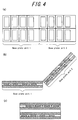
- FIG. 4 is a process diagram illustrating an example of the particularly preferable method for manufacturing the photovoltaic device of the present disclosure described above.
- the photovoltaic device of the present disclosure is manufactured (c) in which, among organic photoelectric conversion module base plates that are adjacent in the stacking direction, at least part of the open section of the organic photoelectric conversion module base plate located on one side in the stacking direction overlaps with at least part of the photoelectric conversion element section of the organic photoelectric conversion module base plate located on an opposite side in the stacking direction.
- the organic photoelectric conversion module base plate units may alternatively be caused to overlap in the opposite direction to that illustrated in (b).
- a photovoltaic device including two layers of stacked organic photoelectric conversion module base plates was obtained by forming two organic photoelectric conversion module base plate units that were electrically connected to one another on a transparent substrate and subsequently performing folding back between the adjacent units to cause overlapping of the adjacent units.
- the base plate units four dye-sensitized solar cells were arranged and connected in series such that a proportion of module base plate area occupied by a photoelectric conversion element section was 50%.
- Each of the dye-sensitized solar cells had the same area.
- a photovoltaic device including three layers of stacked organic photoelectric conversion module base plates was obtained in the same way as in Example 1 in all aspects other than that three organic photoelectric conversion module base plate units were formed on the transparent substrate and the proportion of module base plate area occupied by the photoelectric conversion element section was 35% for each of the base plate units.
- a photovoltaic device including a single organic photoelectric conversion module base plate layer was obtained by forming an organic photoelectric conversion module base plate for which the proportion of module base plate area occupied by a photoelectric conversion element section was 75% using dye-sensitized solar cells having the same configuration as in Example 1 in all aspects other than that a platinum thin-film was used as the catalyst layer of the counter electrode and indium tin oxide (ITO) was used for the conductive films of the photoelectrode and the counter electrode.
- ITO indium tin oxide
- Table 2 indicates that electricity generation in Examples 1 and 2 was 1.8 times higher than in Comparative Example 1 used as the reference, thereby demonstrating that device electricity generation was substantially improved in Examples 1 and 2. Furthermore, manufacturability and processability in device manufacture were highly favorable for Examples 1 and 2.
Landscapes
- Engineering & Computer Science (AREA)
- Power Engineering (AREA)
- Microelectronics & Electronic Packaging (AREA)
- Chemical & Material Sciences (AREA)
- Chemical Kinetics & Catalysis (AREA)
- Electrochemistry (AREA)
- Manufacturing & Machinery (AREA)
- Photovoltaic Devices (AREA)
- Life Sciences & Earth Sciences (AREA)
- Sustainable Development (AREA)
Abstract
Description
- The present disclosure relates to a photovoltaic device including two or more layers of organic photoelectric conversion module base plates that are stacked and connected, and to a method for manufacturing the photovoltaic device.
- A photoelectric conversion module that uses solar cells as photoelectric conversion elements is a known conventional example of a photoelectric conversion module that converts light energy, such as solar energy, to electrical energy. The solar cells are for example silicon (Si) solar cells.
- In recent years, organic solar cells such as dye-sensitized solar cells and organic thin-film solar cells have attracted attention as alternatives to Si solar cells and the like.
- Among such organic solar cells, dye-sensitized solar cells have received particular attention as they are expected to be lighter in weight than, for example, Si solar cells, are capable of generating electricity reliably over a wide illumination range, and can be manufactured from relatively cheap materials without the need for large-scale equipment.
- A dye-sensitized solar cell such as described above typically has a structure in which a
photoelectrode 10, anelectrolyte layer 20, and acounter electrode 30 are arranged in the stated order as illustrated inFIG. 1 . The dye-sensitized solar cell has a mechanism in which electrons are removed from a sensitizing dye in thephotoelectrode 10 upon the sensitizing dye receiving light and the removed electrons move out of thephotoelectrode 10 along anexternal circuit 40 to thecounter electrode 30, before subsequently moving into theelectrolyte layer 20. - It should be noted that in
FIG. 1 ,reference sign 10a indicates a photoelectrode base plate,reference sign 10b indicates a porous semiconductor fine particulate layer,reference sign 10c indicates a sensitizing dye layer,reference signs reference signs reference sign 30b indicates a catalyst layer. - Unfortunately, dye-sensitized solar cells have low photoelectric conversion efficiency and poor electricity generation efficiency compared to, for example, Si solar cells. Consequently, a plurality of dye-sensitized solar cells may be connected to one another in order to improve electricity generation.
- Examples of the above technique are provided by
PTL 1 andPTL 2, which disclose vertically-stacked dye-sensitized solar cell modules that each include a stack of dye-sensitized solar cells in which adjacent dye-sensitized solar cells in the stacking direction are electrically connected to one another. -
- PTL 1:
JP2008-130547 - PTL 2:
JP2013-098005 - In the vertically-stacked dye-sensitized solar cell modules disclosed in
PTL 1 andPTL 2 however, dye-sensitized solar cells serving as photoelectric conversion elements overlap with one another and light transmittance of the cells in generally low, which means that once light has passed through one cell, sufficient light does not reach another cell. Consequently, photoelectric conversion by the other cell is insufficient and the effective area of the cells contributing to photoelectric conversion in the module is reduced, which leaves room for further improvement in terms of increasing electricity generation. - The present disclosure was conceived in order to solve the problem described above and aims to provide a photovoltaic device having high electricity generation. The present disclosure also aims to provide a method for efficiently manufacturing the aforementioned photovoltaic device.
- The inventor performed diligent investigation in order to develop a photovoltaic device having high electricity generation.
- As a result, the inventor discovered that in a configuration in which two or more layers of organic photoelectric conversion module base plates are stacked in order to increase electricity generation, electricity generation can be increased through from 20% to 80% of area of each of the organic photoelectric conversion module base plates being occupied by a photoelectric conversion element section and through the organic photoelectric conversion module base plates being connected such that light that has passed through an upper module base plate can be trapped and undergo photoelectric conversion in a lower module base plate.
- In other words, the present disclosure provides configurations summarized below.
- 1. A photovoltaic device including two or more layers of organic photoelectric conversion module base plates that are stacked and connected, and that each include one or more photoelectric conversion elements, wherein
- from 20% to 80% of area of each of the organic photoelectric conversion module base plates is occupied by a photoelectric conversion element section.
- 2. The photovoltaic device described in 1, wherein each of the organic photoelectric conversion module base plates further includes an open section, and
among organic photoelectric conversion module base plates that are adjacent in a stacking direction, at least part of an open section of an organic photoelectric conversion module base plate located on one side in the stacking direction overlaps in the stacking direction with at least part of a photoelectric conversion element section of an organic photoelectric conversion module base plate located on an opposite side in the stacking direction. - 3. A method for manufacturing a photovoltaic device, including forming two or more electrically connected organic photoelectric conversion module base plate units on a transparent substrate and folding back between adjacent units to cause overlapping of the adjacent units, wherein each of the units includes one or more photoelectric conversion elements, and from 20% to 80% of area of each of the units is occupied by a photoelectric conversion element section.
- 4. The method for manufacturing a photovoltaic device described in 3, wherein each of the units further includes an open section, and open sections and photoelectric conversion element sections are provided in the adjacent units such that when folding back is performed between the adjacent units to cause overlapping of the adjacent units, among units that become adjacent in a stacking direction, at least part of an open section of a unit located on one side in the stacking direction overlaps in the stacking direction with at least part of a photoelectric conversion element section of a unit located on an opposite side in the stacking direction.
- The present disclosure enables acquisition of a photovoltaic device having high electricity generation.
- In the accompanying drawings:
-
FIG. 1 schematically illustrates an example of configuration of a conventional dye-sensitized solar cell; -
FIG. 2 (a) to FIG. 2 (c) are cross-sectional views illustrating examples of a photovoltaic device of the present disclosure; -
FIG. 3 is a plan view illustrating an organic photoelectric conversion module base plate included in a photovoltaic device of the present disclosure; and -
FIG. 4 (a) to FIG. 4 (c) illustrate an exemplary process of a method for manufacturing a photovoltaic device of the present disclosure. - The following provides a specific explanation. First, structure and the like of a photovoltaic device of the present disclosure are explained.
- The photovoltaic device of the present disclosure includes two or more layers of organic photoelectric conversion module base plates that are stacked and electrically connected, and that each include one or more photoelectric conversion elements.
-
FIG. 2 is a cross-sectional view illustrating examples of the photovoltaic device of the present disclosure. As illustrated inFIG. 2 , the organic photoelectric conversion module base plates in the photovoltaic device of the present disclosure can generally adopt three different stacking forms depending on positioning of collection wiring. As illustrated inFIG. 2 , collection wiring is typically only located in contact with one out of a lower substrate and an upper substrate of an organic photoelectric conversion module base plate. However, collection wiring may alternatively be located in contact with both substrates and in such a situation, the organic photoelectric conversion module base plates only have one stacking form because there is no difference caused by positioning of the collection wiring. - It should be noted that in
FIG. 2 ,reference sign 50 indicates the photovoltaic device,reference sign 50a indicates a side wall,reference sign 60 indicates an organic photoelectric conversion module base plate,reference sign 60a indicates substrates,reference sign 60b indicates a photoelectric conversion element,reference sign 60c indicates collection wiring, andreference sign 60d indicates an open section. - As illustrated in
FIG. 2 , the open section (inclusive of a collection wiring section) is normally a base plate region in which photoelectric conversion elements are not present. Although the open section may be hollow, it is generally preferable that the open section is sealed with a transparent resin such as described further below. An open section such as described above has higher light transmittance than a region in which a photoelectric conversion element is present. Therefore, organic photoelectric conversion module base plates that are adjacent in a stacking direction are preferably stacked such that at least part of an open section of an organic photoelectric conversion module base plate located on one side in the stacking direction overlaps in the stacking direction with at least part of photoelectric conversion elements of an organic photoelectric conversion module base plate located on an opposite side in the stacking direction. - The stacking described above can enable irradiated light to reach a lower module base plate more efficiently, can increase the effective area of photoelectric conversion elements contributing to photoelectric conversion, and can improve electricity generation.
- Sufficiently high effective area of photoelectric conversion elements contributing to photoelectric conversion and high electricity generation can for example be achieved by adopting a configuration in which, among organic photoelectric conversion module base plates that are adjacent in the stacking direction, at least part of an open section of an organic photoelectric conversion module base plate located on one side in the stacking direction overlaps with at least part of photoelectric conversion elements of an organic photoelectric conversion module base plate located on an opposite side in the stacking direction, and in which an overlapping region of photoelectric conversion elements of an upper module base plate and a module base plate below the upper module base plate is preferably from 0% to 50%, and more preferably from 0% to 30%, of the area occupied by the photoelectric conversion elements in the lower module base plate. In particular, a configuration in which the photoelectric conversion elements of the upper module base plate and the lower module base plate partially overlap is favorable because the photoelectric conversion elements of the lower module base plate can trap light that is incident diagonally from the open section of the upper module base plate.
- In a configuration in which three layers of organic photoelectric conversion module base plates (referred to as a first layer, a second layer, and a third layer in order from a direction in which light is irradiated) are stacked, the first layer is an upper module base plate and the second layer is a lower module base plate in a relationship between the first and second layers, and the second layer is an upper module base plate and the third layer is a lower module base plate in a relationship between the second and third layers. The same applies in a configuration in which four or more layers of organic photoelectric conversion module base plates are stacked.
- From a viewpoint of optimizing electricity generation and manufacturing cost, it is preferable that the number of stacked layers of organic photoelectric conversion module base plates is approximately from 2 to 5 layers.
- Furthermore, from a viewpoint of efficiently taking incident light into the lower module base plate, it is preferable that an interval "a" between the organic photoelectric conversion module base plates (distance between the upper module base plate and the lower module base plate, refer to
FIG. 2 ) is in a range from 10 nm to 5 mm, and more preferably in a range from 100 nm to 3 mm. - Explanation is provided next for the organic photoelectric conversion module base plates included in the photovoltaic device of the present disclosure.
- Each of the organic photoelectric conversion module base plates included in the photovoltaic device of the present disclosure includes one or more photoelectric conversion elements.
- The organic photoelectric conversion module base plate for example has a configuration such as illustrated in
FIG. 3 , in which photoelectric conversion elements are arranged on a substrate that serves as a support and in which the photoelectric conversion elements are electrically connected to one another in series or parallel through collection wiring (not all of the wiring is illustrated). A base plate region in which the photoelectric conversion elements are not present is normally an open section (inclusive of a collection wiring section). - From a viewpoint of increasing light transmittance of the photoelectric conversion elements and the open section of the organic photoelectric conversion module base plate, it is preferable that the substrate is a transparent substrate. Examples of transparent substrates that can be used include a glass substrate and a transparent resin substrate made from a transparent resin such as described further below. Herein, the term "transparent" is used to refer to a light transmittance of at least 70% (preferably at least 80%). The light transmittance is a total light transmittance measured in accordance with JIS K7361-1.
- From a viewpoint of balance between light transmittance and strength, it is preferable that the transparent substrate has a thickness in a range from 0.01 mm to 10 mm.
- The following characteristic of the organic photoelectric conversion module base plate is one of the main features of the present disclosure.
- From 20% to 80% of area of the organic photoelectric conversion module base plate is occupied by a photoelectric conversion element section.
- In order to ensure sufficient electricity generation per layer of module base plates while also increasing light transmittance of the upper module base plate, ensuring sufficient light is incident on the lower module base plate, and increasing the effective area of photoelectric conversion elements contributing to electricity generation to improve device electricity generation, the photoelectric conversion element section is required to occupy from 20% to 80% of area of the organic photoelectric conversion module base plate used in the present disclosure. From a viewpoint of ensuring sufficient device performance while also simplifying formation of the photoelectric conversion elements and the collection wiring, and reducing manufacturing costs, the proportion of area occupied by the photoelectric conversion element section is preferably from 35% to 65%, and more preferably from 40% to 60%.
- Herein, the proportion of area of the organic photoelectric conversion module base plate that is occupied by the photoelectric conversion element section is not necessarily the same for both the upper module base plate and the lower module base plate.
- Explanation is provided next for the photoelectric conversion elements that are arranged in the organic photoelectric conversion module base plate described above.
- The photoelectric conversion elements arranged in the organic photoelectric conversion module base plate can be commonly known dye-sensitized solar cells or organic thin-film solar cells. However, use of dye-sensitized solar cells is more advantageous in terms of, for example, cost and ease of manufacture.
- The following explains an example of a dye-sensitized solar cell that can be used.
- As described further above with reference to
FIG. 1 , a dye-sensitized solar cell typically has a structure in which a photoelectrode (transparent electrode) 10, anelectrolyte layer 20, and acounter electrode 30 are arranged in the stated order. - The
photoelectrode 10 includes aphotoelectrode base plate 10a, a porous semiconductorfine particulate layer 10b formed on thephotoelectrode base plate 10a, and a sensitizingdye layer 10c formed by a sensitizing dye adsorbed onto the surface of the porous semiconductor fine particulate layer. - The
photoelectrode base plate 10a functions as a support for the porous semiconductorfine particulate layer 10b, etc., and also functions as a current collector. - The
photoelectrode base plate 10a for example includes a transparent resin substrate or glass substrate as asupport 10d and aconductive layer 10e stacked thereon that is made from a composite metal oxide such as indium tin oxide (ITO) or indium zinc oxide (IZO). Although no specific limitations are placed on thesupport 10d, the function of thesupport 10d is normally implemented by a substrate of an organic photoelectric conversion module base plate included in the photovoltaic device of the present disclosure. - Examples of transparent resins that can be used include synthetic resins such as cycloolefin polymer (COP), polyethylene terephthalate (PET), polyethylene naphthalate (PEN), syndiotactic polystyrene (SPS), polyphenylene sulfide (PPS), polycarbonate (PC), polyarylate (PAr), polysulfone (PSF), polyester sulfone (PES), polyetherimide (PEI), and transparent polyimide (PI).
- The porous semiconductor
fine particulate layer 10b is a porous layer that contains semiconductor fine particles. As a result of the layer being porous, sensitizing dye adsorption can be increased and a dye-sensitized solar cell having a high conversion efficiency can be more easily obtained. - Examples of semiconductor fine particles that can be used include particles of metal oxides such as titanium oxide, zinc oxide, and tin oxide.
- The porous semiconductor fine particulate layer can be formed by a commonly known method such as a press method, a hydrothermal decomposition method, an electrophoretic deposition method, or a binder-free coating method.
- The sensitizing
dye layer 10c is a layer of a compound (sensitizing dye) that is adsorbed onto the surface of the porous semiconductorfine particulate layer 10b and that can transfer electrons to the porous semiconductorfine particulate layer 10b upon being excited by light. It should be noted that the same sensitizing dye may be used in each of the dye-sensitized solar cells forming the photoelectric conversion elements of the present disclosure, or different sensitizing dyes may be used in different dye-sensitized solar cells. - Examples of sensitizing dyes that can be used include organic dyes such as cyanine dyes, merocyanine dyes, oxonol dyes, xanthene dyes, squarylium dyes, polymethine dyes, coumarin dyes, riboflavin dyes, and perylene dyes, and metal complex dyes such as phthalocyanine complexes and porphyrin complexes of metals such as iron, copper, and ruthenium.
- The sensitizing
dye layer 10c can for example be formed by a commonly known method such as a method in which the porous semiconductorfine particulate layer 10b is immersed in a solution of the sensitizing dye or a method in which a solution of the sensitizing dye is applied onto the porous semiconductorfine particulate layer 10b. - It should be noted that so long as the photoelectrode can release electrons into the
external circuit 40 as a result of receiving light, the photoelectrode is not limited to the photoelectrode illustrated inFIG. 1 . - The
electrolyte layer 20 is a layer that is provided in order to separate thephotoelectrode 10 and thecounter electrode 30, and also in order to enable efficient charge movement. - The
electrolyte layer 20 typically contains a supporting electrolyte, a redox couple (i.e., a couple of chemical species that can be reversibly converted between in a redox reaction in the form of an oxidant and a reductant), a solvent, and so forth. - Examples of supporting electrolytes that can be used include salts having a cation such as a lithium ion, an imidazolium ion, or a quaternary ammonium ion.
- The redox couple enables reduction of the oxidized sensitizing dye and examples thereof include chlorine compound/chlorine, iodine compound/iodine, bromine compound/bromine, thallium(III) ions/thallium(I) ions, ruthenium(III) ions/ruthenium(II) ions, copper(II) ions/copper(I) ions, iron(III) ions/iron(II) ions, cobalt(III) ions/cobalt(II) ions, vanadium(III) ions/vanadium(II) ions, manganic acid ions/permanganic acid ions, ferricyanide/ferrocyanide, quinone/hydroquinone, and fumaric acid/succinic acid.
- Examples of solvents that can be used include solvents used for forming electrolyte layers in solar cells such as acetonitrile, methoxyacetonitrile, methoxypropionitrile, N,N-dimethylformamide, ethylmethylimidazolium bis(trifluoromethylsufonyl)imide, and propylene carbonate.
- The
electrolyte layer 20 can for example be formed by applying a solution (electrolyte solution) including the components of theelectrolyte layer 20 onto thephotoelectrode 10 or by preparing a cell including thephotoelectrode 10 and thecounter electrode 30 and then injecting the electrolyte solution into a gap between the electrodes. - The
counter electrode 30 is for example formed by forming aconductive film 30c on asupport 30a and forming acatalyst layer 30b on theconductive film 30c. - The
support 30a and theconductive film 30c can for example be the same as described above for thephotoelectrode base plate 10a. Thecatalyst layer 30b may be optionally provided to function as a catalyst for transferring electrons from the counter electrode to the electrolyte layer and is typically formed by a platinum thin-film. Furthermore, the function of thesupport 30a may be implemented by a substrate of an organic photoelectric conversion module base plate included in the photovoltaic device of the present disclosure. - It should be noted that the
conductive film 30c is not essential in a configuration in which thecatalyst layer 30b is conductive; however, provision of theconductive film 30c is preferable from a viewpoint of ensuring favorable electrical continuity. - Although the above has explained an example of a dye-sensitized solar cell that can be used in the present disclosure, it is highly advantageous in the present disclosure to adopt carbon nanotubes or metal nanoparticle-supporting carbon nanotubes in the catalyst layer of the counter electrode described above or to adopt conductors containing carbon nanotubes or containing carbon nanotubes and metal nanostructures as the conductive films of the photoelectrode and the counter electrode.
- That is to say, compared to a configuration in which a conventional platinum thin-film or composite metal oxide such as indium tin oxide (ITO) is adopted, catalytic activity and conductivity can be raised, cell electricity generation efficiency can be increased, and a larger open section can for example be provided in the organic photoelectric conversion module base plate. Furthermore, producibility can be significantly improved by for example performing cell production by a roll-to-roll process. Therefore, device electricity generation can be improved while also enabling simplified manufacturing and reduced manufacturing cost.
- The following explains the carbon nanotubes, the metal nanoparticle-supporting carbon nanotubes, and the conductors containing carbon nanotubes or containing carbon nanotubes and metal nanostructures.
- Although a platinum thin-film is typically used as the catalyst layer of the counter electrode, carbon nanotubes-in particular, carbon nanotubes (also referred to below as carbon nanotubes (A)) having an average diameter (Av) and a diameter standard deviation (σ) that satisfy 0.60 > 3σ/Av > 0.20 (preferably, 0.60 > 3σ/Av > 0.50)-and such carbon nanotubes (A) further supporting metal nanoparticles are examples of preferable alternative materials that can be used.
- That is to say, use of such materials is highly advantageous for mass production because manufacturing cost can be substantially reduced compared to that of platinum thin-films, the catalyst layer can be formed through application and drying of a dispersion liquid in which carbon nanotubes are dispersed, the dispersion liquid has favorable application properties, processability accuracy is significantly improved, and high-speed application by a roll-to-roll process and processed film manufacture are facilitated.
- In addition, compared to a configuration in which a conventional platinum thin-film is used, catalytic activity can be raised and cell electricity generation efficiency can be increased. Therefore, light transmittance of the module base plate can be increased, for example by increasing the size of the open section, while also maintaining a balance with manufacturability.
- It should be noted that the term "carbon nanotubes (A)" is used herein as a general term for a carbon nanotube assembly of specific carbon nanotubes composing the carbon nanotubes (A) and the term "diameter" is used herein to refer to the external diameter of the specific carbon nanotubes. Furthermore, the average diameter (Av) and the diameter standard deviation (σ) are respectively an average value and a standard deviation obtained by measuring the diameter of 100 randomly selected carbon nanotubes through observation under a transmission electron microscope (average length described further below is an average value obtained by measuring length through the same method). In the present disclosure, the carbon nanotubes (A) that are used typically take a normal distribution when a plot is made of diameter measured as described above on a horizontal axis and frequency on a vertical axis, and a Gaussian approximation is made.
- Herein, from a viewpoint of achieving excellent catalytic activity, the average diameter (Av) of the carbon nanotubes (A) described above is preferably at least 0.5 nm and no greater than 15 nm, and more preferably at least 1 nm and no greater than 10 nm.
- In addition, the average length of the carbon nanotubes (A) is preferably from 0.1 µm to 1 cm, and more preferably from 0.1 µm to 1 mm. As a result of the average length of the carbon nanotubes (A) being in the range described above, carbon nanotube orientation can be improved and thin-film formation can be easily performed, thus facilitating formation of a catalyst layer having high activity.
- The carbon nanotubes (A) preferably have a specific surface area of from 100 m2/g to 2,500 m2/g, and more preferably from 400 m2/g to 1,600 m2/g. Formation of a catalyst layer having high activity is facilitated by the specific surface area of the carbon nanotubes (A) being in the range described above.
- The specific surface area of the carbon nanotubes (A) can be obtained through a nitrogen gas adsorption method.
- The carbon nanotubes composing the carbon nanotubes (A) may be single-walled carbon nanotubes or multi-walled carbon nanotubes. However, carbon nanotubes having from one to five walls are preferable and single-walled carbon nanotubes are more preferable from a viewpoint of improving activity of the catalyst layer.
- The carbon nanotubes composing the carbon nanotubes (A) may have a functional group such as a carboxyl group introduced onto the surface thereof. The functional group may be introduced by commonly known oxidation treatment using hydrogen peroxide, nitric acid, or the like.
- Furthermore, the carbon nanotubes composing the carbon nanotubes (A) preferably have micropores. Among carbon nanotubes having micropores, carbon nanotubes having micropores that have a pore diameter of smaller than 2 nm are preferable. In terms of the amount of micropores present, the micropore volume as obtained through a method described below is preferably at least 0.4 mL/g, more preferably at least 0.43 mL/g, and particularly preferably at least 0.45 mL/g, and typically has an upper limit of approximately 0.65 mL/g. It is preferable that the carbon nanotubes have micropores such as described above from a viewpoint of improving catalytic activity. The micropore volume can for example be adjusted through appropriate alteration of a preparation method and preparation conditions of the carbon nanotubes.
- Herein, "micropore volume (Vp)" can be calculated from equation (I)-Vp = (V/22,414) × (M/ρ)-by measuring a nitrogen adsorption and desorption isotherm of the carbon nanotubes at liquid nitrogen temperature (77 K) and by setting an amount of adsorbed nitrogen at a relative pressure P/P0 = 0.19 as V. It should be noted that P is a measured pressure at adsorption equilibrium, P0 is a saturated vapor pressure of liquid nitrogen at time of measurement, and, in equation (I), M is a molecular weight of 28.010 of the adsorbate (nitrogen), and ρ is a density of 0.808 g/cm3 of the adsorbate (nitrogen) at 77 K. The micropore volume can for example be easily obtained using a "BELSORP (registered trademark)-mini" (product of Bel Japan Inc.).
- The carbon nanotubes (A) having the properties described above can for example be manufactured efficiently by, in a method (super growth method; refer to
WO2006/011655 ) in which, during synthesis of carbon nanotubes through chemical vapor deposition (CVD) by supplying a feedstock compound and a carrier gas onto a substrate (also referred to below as a "substrate for CNT manufacture") having a catalyst layer for carbon nanotube manufacture (also referred to below as a "catalyst layer for CNT manufacture") on the surface thereof, catalytic activity of the catalyst layer for CNT manufacture is dramatically improved by providing a trace amount of an oxidizing agent in the system, forming the catalyst layer on the surface of the substrate through a wet process (carbon nanotubes obtained through the super growth method described above are also referred to below as a SGCNTs). - The carbon nanotubes (A) may support metal nanoparticles, which is expected to improve catalytic effect.
- Examples of metal nanoparticles that can be used include nanoparticles of metals in groups 6 to 14 of the periodic table.
- Examples of metals in groups 6 to 14 of the periodic table include Cr, Mn, Fe, Co, Ni, Cu, Zn, Ga, Ru, Rh, Pd, Ag, Cd, Sn, Sb, W, Re, Ir, Pt, Au, and Pb. Among the metals listed above, Fe, Co, Ni, Ag, W, Ru, Pt, Au, and Pd are preferable for obtaining a highly versatile oxidation/reduction catalyst.
- Any one of the metals listed above or a combination of any two or more of the metals listed above may be used.
- From a viewpoint of improving catalytic effect, the metal nanoparticles preferably have an average particle diameter from 0.5 nm to 15 nm and preferably have a particle diameter standard deviation of no greater than 1.5 nm.
- Although no specific limitations are placed on the amount of supported metal nanoparticles, the amount is preferably at least 1 part by mass per 100 parts by mass of the carbon nanotubes (A). As a result of the amount of supported metal nanoparticles being at least 1 part by mass, even better catalytic activity can be achieved. Although it is thought that catalytic activity continues to increase with increasing amount of supported metal nanoparticles, when supporting ability of the carbon nanotubes (A) and economic factors are taken into account, an upper limit for the amount of metal nanoparticles is, in general, preferably no greater than 30,000 parts by mass per 100 parts by mass of the carbon nanotubes (A).
- No specific limitations are placed on the method by which the metal nanoparticles are caused to be supported by the carbon nanotubes. For example, the metal nanoparticles can be caused to be supported by the carbon nanotubes through a commonly known method in which a metal precursor is reduced in the presence of the carbon nanotubes (A) to produce the metal nanoparticles.
- More specifically, a dispersion liquid including water, the carbon nanotubes (A), and a dispersant is prepared and solvent is evaporated after addition of the metal precursor. Next, heating is performed under hydrogen gas flow to reduce the metal precursor, thereby efficiently obtaining a metal nanoparticle support of produced metal nanoparticles supported by the carbon nanotubes (A).
- The catalyst layer of the counter electrode can for example be formed by preparing a dispersion liquid including the carbon nanotubes (A), applying the prepared dispersion liquid onto the support, and drying the applied film.
- Examples of solvents that can be used to prepare the dispersion liquid include water, alcohols such as methanol, ethanol, and propanol, ketones such as acetone and methyl ethyl ketone, ethers such as tetrahydrofuran, dioxane, and diglyme, amides such as N,N-dimethylformamide, N,N-dimethylacetamide, N-methyl-2-pyrrolidone, and 1,3-dimethyl-2-imidazolidinone, and sulfur-containing solvents such as dimethyl sulfoxide and sulfolane. Any one of the solvents listed above or a combination of any two or more of the solvents listed above may be used.
- The dispersion liquid may further include other components such as a binder, a conductive additive, a dispersant, and a surfactant. Commonly known components may be used as appropriate as such components.
- The dispersion liquid can for example be prepared by mixing the carbon nanotubes (A) and other components, as required, in the solvent and dispersing the carbon nanotubes.
- Mixing treatment or dispersing treatment can for example be carried out through a method using a nanomizer, an ultimizer, an ultrasonic disperser, a ball mill, a sand grinder, a dyno-mill, a spike mill, a DCP mill, a basket mill, a paint conditioner, or a high-speed stirring device.
- Application of the dispersion liquid onto a substrate can for example be carried out by dipping, roll coating, gravure coating, knife coating, air knife coating, roll knife coating, die coating, screen printing, spray coating, or gravure offset.
- Drying of the applied film can for example be carried out by hot-air drying, hot-roll drying, or infrared irradiation. Although no specific limitations are placed on the drying temperature and time, the drying temperature is normally from room temperature to 200°C and the drying time is normally from 0.1 minutes to 150 minutes.
- Also, although no specific limitations are placed on the amount of the carbon nanotubes (A) in the dispersion liquid, the amount of the carbon nanotubes (A) is preferably from 0.001% by mass to 10% by mass of the total mass of the dispersion liquid, and more preferably from 0.01% by mass to 5% by mass.
- Conductive films made for example from a composite metal oxide such as indium tin oxide (ITO) or indium zinc oxide (IZO) are generally used as the conductive films of the photoelectrode and the counter electrode. However, a preferable alternative that can be used is a conductor (also referred to below as conductive layer (I)) containing the carbon nanotubes (A) described above or containing the carbon nanotubes (A) and metal nanostructures.
- That is to say, such a conductive film is highly advantageous for mass production because the conductive film can be formed by applying and drying a dispersion liquid in which the carbon nanotubes are dispersed or in which the carbon nanotubes and the metal nanostructure are dispersed, the dispersion liquid has favorable application properties, processability accuracy is significantly improved, and high-speed application by roll-to-roll and processed film manufacture are facilitated.
- In addition, compared to a conventional configuration in which a composite metal oxide such as indium tin oxide (ITO) is used, conductivity and cell electricity generation efficiency can be increased. Therefore, light transmittance of the module base plate can be increased, for example by increasing the size of the open section, while also achieving a balance with manufacturability.
- The metal nanostructures described above are fine structures made from a metal or a metal compound and are used as a conductor.
- No particular limitations are placed on the metal or metal compound composing the metal nanostructures other than being conductive. Possible examples include metals such as copper, silver, platinum and gold, metal oxides such as indium oxide, zinc oxide, and tin oxide, and composite metal oxides such as aluminum zinc oxide (AZO), indium tin oxide (ITO), and indium zinc oxide (IZO).
- Among the above examples, silver or platinum is preferable due to the ease of obtaining excellent conductivity and transparency.
- Examples of possible metal nanostructures include metal nanoparticles, metal nanowires, metal nanorods, and metal nanosheets.
- Among the metal nanostructures listed above, metal nanoparticles are particulate structures having a nanometer scale average particle diameter. Although no specific limitations are placed on the average particle diameter of the metal nanoparticles (average particle diameter of primary particles), the average particle diameter is preferably from 10 nm to 300 nm. As a result of the average particle diameter being in the range described above, it is easier to obtain a conductive film having excellent conductivity and transparency.
- The average particle diameter of the metal nanoparticles can be calculated by measuring the particle diameter of 100 randomly selected metal nanoparticles using a transmission electron microscope. The size of other metal nanostructures explained below can be obtained by the same method.
- The metal nanoparticles can for example be obtained by a commonly known method such as a polyol method in which an organic complex is reduced by a polyhydric alcohol to synthesize metal nanoparticles or a reverse micelle method in which a reverse micelle solution including a reductant and a reverse micelle solution including a metal salt are mixed to synthesize metal nanoparticles.
- Metal nanowires are linear structures having a nanometer scale average diameter and an aspect ratio (length/diameter) of at least 10. Although no specific limitations are placed on the average diameter of the metal nanowires, the average diameter is preferably from 10 nm to 300 nm. Also, although no specific limitations are placed on the average length of the metal nanowires, the average length is preferably at least 3 µm.
- As a result of the average diameter and the average length being in the ranges described above, it is easier to obtain a conductive film having excellent conductivity and transparency.
- The metal nanowires can for example be obtained by a commonly known method such as a method in which an applied voltage or current is imparted on the surface of a precursor from a tip of a probe and a metal nanowire is pulled out by the probe tip to continuously form the metal nanowire (
JP2004-223693 JP2002-266007 - Metal nanorods are cylindrical structures having a nanometer scale average diameter and an aspect ratio (length/diameter) of at least 1 and less than 10. Although no specific limitations are placed on the average diameter of the nanorods, the average diameter is preferably from 10 nm to 300 nm. Also, although no specific limitations are placed on the average length of the nanorods, the average length is preferably from 10 nm to 3,000 nm.
- As a result of the average diameter and the average length being in the ranges described above, it is easier to obtain a conductive film having excellent conductivity and transparency.
- The metal nanorods can for example be obtained by a commonly known method such as electrolysis, chemical reduction, or photoreduction.
- Metal nanosheets are sheet-shaped structures having a nanometer scale thickness. Although no specific limitations are placed on the thickness of the metal nanosheets, the thickness is preferably from 1 nm to 10 nm. Also, although no specific limitations are placed on the size of the metal nanosheets, a side length of the metal nanosheets is preferably from 0.1 µm to 10 µm. As a result of the thickness and the side length being in the ranges described above, it is easier to obtain a conductive film having excellent conductivity and transparency.
- The metal nanosheets can be obtained by a commonly known method such as a method in which a layered compound is peeled, chemical vapor deposition, or a hydrothermal method.
- Among the metal nanostructures described above, use of metal nanowires is preferable in terms of ease of achieving excellent conductivity and transparency.
- Any one of the types of metal nanostructures listed above or a combination of any two or more of the types of metal nanostructures listed above may be used.
- Although no specific limitations are placed on the amount of the metal nanostructures in the conductive layer (I) described above, the amount is preferably from 0.0001 mg/cm2 to 0.05 mg/cm2.
- Furthermore, the amount of the carbon nanotubes (A) in the conductive layer (I) is preferably from 1.0×10⁻⁶ mg/cm2 to 30 mg/cm2.
- As a result of the amounts of the metal nanostructures and the carbon nanotubes (A) being in the ranges described above, conductivity and transparency are further improved.
- Although no specific limitations are placed on the thickness of the conductive layer (I), the thickness is typically from 100 nm to 1 mm. As a result of the thickness of the conductive layer being in the range described above, favorable conductivity and transparency can be achieved.
- The conductive layer (I) may contain other components such as a binder, a conductive additive, a dispersant, and a surfactant to the extent that such components do not adversely affect conductivity and transparency.
- Furthermore, a conductive layer (also referred to as conductive layer (II)) containing the metal nanostructures described above may be further provided between the support and the conductive layer described above in each of the electrodes.
- Although no specific limitations are placed on the amount of the metal nanostructures in the conductive layer (II), the amount is preferably from 0.0001 mg/cm2 to 0.2 mg/cm2. As a result of the amount of the metal nanostructures being in the range described above, conductivity and transparency can be further improved.
- Although no specific limitations are placed on the thickness of the conductive layer (II), the thickness is normally from 30 nm to 1 mm. As a result of the thickness of the conductive layer (II) being in the range described above, favorable conductivity and transparency can be achieved.
- The conductive layer (II) may contain components other than the metal nanostructures to the extent that such components do not adversely affect conductivity and transparency. Examples of other components that can be used are the same as the examples of other components given for the conductive layer (I).
- Furthermore, other layers such as a hard coating layer, a gas barrier layer, and an adhesive layer may also be provided to the extent that such layers do not adversely affect conductivity and transparency. Such layers can be formed by commonly known conventional methods.
- The conductive layer (I) described above can for example be obtained by preparing a dispersion liquid including the metal nanostructures and the carbon nanotubes (A), applying the dispersion liquid onto the support acting as a substrate, and drying the resultant applied film to form a conductive layer.
- The dispersion liquid can be prepared in the same way as described above for formation of the catalyst layer. Furthermore, application and drying can also be carried out in the same way as described above for formation of the catalyst layer.
- As explained above, in the photovoltaic device of the present disclosure, adoption of carbon nanotubes or metal nanoparticle-supporting carbon nanotubes in the catalyst layer of the counter electrode of the dye-sensitized solar cell or adoption of conductors containing carbon nanotubes or containing carbon nanotubes and metal nanostructures as the conductive films of the photoelectrode and the counter electrode of the dye-sensitized solar cell can substantially reduce manufacturing cost. Furthermore, such a catalyst layer or conductive film is highly advantageous for mass production because the layer or film can be formed through application and drying of a dispersion liquid in which the carbon nanotubes are dispersed, the dispersion liquid has favorable application properties, processability accuracy is significantly improved, and high-speed application by roll-to-roll and processed film manufacture are facilitated.
- In addition, compared to a conventional configuration in which a platinum thin-film or indium tin oxide (ITO) is used, catalytic activity and conductivity can be raised, and cell electricity generation efficiency can be increased. Therefore, light transmittance of the module base plate can be increased, for example by increasing the size of the open section, while also achieving a balance with manufacturability.
- The following explains a method for manufacturing the photovoltaic device of the present disclosure.
- Although no specific limitations are placed on manufacture of the photovoltaic device of the present disclosure, the photovoltaic device can for example be manufactured by stacking and electrically connecting two or more layers of organic photoelectric conversion module base plates that are each formed by arranging photoelectric conversion elements described above on a transparent substrate at fixed intervals such that the elements occupy a specific proportion of area of the resultant organic photoelectric conversion module base plate and electrically connecting the photoelectric conversion elements to one another by collection wiring. Formation of the photoelectric conversion elements, patterning of the collection wiring, and so forth can be carried out in accordance with commonly known methods.
- Among such methods, a particularly suitable method includes a process in which two or more layers of organic photoelectric conversion module base plates are stacked by forming two or more organic photoelectric conversion module base plate units that are electrically connected to one another on a transparent substrate and folding back between adjacent units to cause overlapping of the adjacent units. The above-described method improves the yield and also, for example, enables manufacture by a roll-to-roll process when carbon nanotubes are used in formation of the photoelectric conversion elements, enables cost reduction, and enables reliable and efficient manufacture of the photovoltaic device of the present disclosure. In the method described above, open sections and photoelectric conversion element sections are preferably provided in the adjacent units such that when folding back is performed between the adjacent units to cause overlapping of the adjacent units, among units that are adjacent in the stacking direction, at least part of the open section of the unit located on one side in the stacking direction overlaps in the stacking direction with at least part of the photoelectric conversion element section of the unit located on an opposite side in the stacking direction. Note that formation of the organic photoelectric conversion module base plate units on the transparent substrate can be carried out in accordance with the formation method for an organic photoelectric conversion module base plate described above. The organic photoelectric conversion module base plate units may be formed in an arrangement such that the position of the collection wiring relative to the transparent substrate is the same for each unit, may be formed in an arrangement such that the position of the collection wiring relative to the transparent substrate is different for each unit, or may be formed in an arrangement which is a mixture of the arrangements described above.
-
FIG. 4 is a process diagram illustrating an example of the particularly preferable method for manufacturing the photovoltaic device of the present disclosure described above. In the embodiment inFIG. 4 , by (a) forming two base plate units on a transparent substrate with each of the units being the same as the organic photoelectric conversion module base plate illustrated inFIG. 3 , and (b) performing folding back between adjacent units to cause overlapping of the adjacent units and form two layers of organic photoelectric conversion module base plates, the photovoltaic device of the present disclosure is manufactured (c) in which, among organic photoelectric conversion module base plates that are adjacent in the stacking direction, at least part of the open section of the organic photoelectric conversion module base plate located on one side in the stacking direction overlaps with at least part of the photoelectric conversion element section of the organic photoelectric conversion module base plate located on an opposite side in the stacking direction. It should be noted that the organic photoelectric conversion module base plate units may alternatively be caused to overlap in the opposite direction to that illustrated in (b). - A photovoltaic device including two layers of stacked organic photoelectric conversion module base plates was obtained by forming two organic photoelectric conversion module base plate units that were electrically connected to one another on a transparent substrate and subsequently performing folding back between the adjacent units to cause overlapping of the adjacent units. In each of the base plate units, four dye-sensitized solar cells were arranged and connected in series such that a proportion of module base plate area occupied by a photoelectric conversion element section was 50%. Each of the dye-sensitized solar cells had the same area.
- In each of the dye-sensitized solar cells, the catalyst layer of the counter electrode was formed by SGCNTs (carbon nanotubes composed mainly of single-walled CNTs, 3σ/Av = 0.58 (Av: average diameter, σ: diameter standard deviation), average diameter (Av) 3.3 nm, diameter distribution (3σ) 1.9 nm, specific surface area 804 m2/g, average length 500 µm, micropore volume 0.44 mL/g) prepared by a super growth method in accordance with the contents of
WO2006/011655 , and conductors containing the same carbon nanotubes were used as the conductive films of the photoelectrode and the counter electrode. Other aspects of configuration were the same as in a conventional dye-sensitized solar cell. - A photovoltaic device including three layers of stacked organic photoelectric conversion module base plates was obtained in the same way as in Example 1 in all aspects other than that three organic photoelectric conversion module base plate units were formed on the transparent substrate and the proportion of module base plate area occupied by the photoelectric conversion element section was 35% for each of the base plate units.
- A photovoltaic device including a single organic photoelectric conversion module base plate layer was obtained by forming an organic photoelectric conversion module base plate for which the proportion of module base plate area occupied by a photoelectric conversion element section was 75% using dye-sensitized solar cells having the same configuration as in Example 1 in all aspects other than that a platinum thin-film was used as the catalyst layer of the counter electrode and indium tin oxide (ITO) was used for the conductive films of the photoelectrode and the counter electrode.
[Table 1] No. of module base plate stacked layers Proportion of module base plate area occupied by photoelectric conversion element section (%) Example 1 2 First layer 50 Second layer 50 Example 2 3 First layer 35 Second layer 35 Third layer 35 Comparative Example 1 1 First layer 75 - Electricity generation, manufacturability, and processability of the photovoltaic devices obtained as described above were evaluated as follows.
- Each of the photovoltaic devices obtained as described above was connected to a sourcemeter (Series 2400 SourceMeter produced by Keithley Instruments) under illumination conditions of 10,000 lux and electricity generation was measured. The measurement results are shown in Table 2.
- It should be noted that results are shown as ratios relative to a standard value; herein, the standard value is set as a value of electricity generation (and voltage) per unit area of the device in Comparative Example 1.
- With regards to manufacturability and processability, difficulty of (a) patterning, (b) electrode bonding, and (c) module base plate assembly in the manufacturing process of each of the photovoltaic devices was evaluated in accordance with the three levels shown below. The evaluation results are also shown in Table 2.
- Excellent: Implementable in a short period of time, without defects, etc., through standard control
- Good: Implementable without defects, etc., through standard control
- Fair: Implementable without defects, etc., through precise control
- Table 2 indicates that electricity generation in Examples 1 and 2 was 1.8 times higher than in Comparative Example 1 used as the reference, thereby demonstrating that device electricity generation was substantially improved in Examples 1 and 2. Furthermore, manufacturability and processability in device manufacture were highly favorable for Examples 1 and 2.
-
- 10
- photoelectrode
- 10a
- photoelectrode base plate
- 10b
- porous semiconductor fine particulate layer
- 10c
- sensitizing dye layer
- 10d
- support
- 10e
- conductive film
- 20
- electrolyte layer
- 30
- counter electrode
- 30a
- support
- 30b
- catalyst layer
- 30c
- conductive film
- 40
- external circuit
- 50
- photovoltaic device
- 50a
- side wall
- 60
- organic photoelectric conversion module base plate
- 60a
- substrate
- 60b
- photoelectric conversion element
- 60c
- collection wiring
- 60d
- open section
| Electricity generation | Voltage | Manufacturability and processability | |||
| (a) Patterning | (b) Bonding | (c) Assembly | |||
| Example 1 | 1.8 | 1 | Excellent | Excellent | Excellent |
| Example 2 | 1.8 | 1 | Excellent | Excellent | Good |
| Comparative Example 1 | 1 | 1 | Fair | Fair | Excellent |
Claims (4)
- A photovoltaic device comprising
two or more layers of organic photoelectric conversion module base plates that are stacked and connected, and that each include one or more photoelectric conversion elements, wherein
from 20% to 80% of area of each of the organic photoelectric conversion module base plates is occupied by a photoelectric conversion element section. - The photovoltaic device of claim 1, wherein
each of the organic photoelectric conversion module base plates further includes an open section, and
among organic photoelectric conversion module base plates that are adjacent in a stacking direction, at least part of an open section of an organic photoelectric conversion module base plate located on one side in the stacking direction overlaps in the stacking direction with at least part of a photoelectric conversion element section of an organic photoelectric conversion module base plate located on an opposite side in the stacking direction. - A method for manufacturing a photovoltaic device, comprising
stacking two or more layers of organic photoelectric conversion module base plates by forming two or more connected organic photoelectric conversion module base plate units on a transparent substrate and folding back between adjacent units to cause overlapping of the adjacent units, wherein
each of the units includes one or more photoelectric conversion elements, and
from 20% to 80% of area of each of the units is occupied by a photoelectric conversion element section. - The method for manufacturing a photovoltaic device of claim 3, wherein
each of the units further includes an open section, and
open sections and photoelectric conversion element sections are provided in the adjacent units such that when folding back is performed between the adjacent units to cause overlapping of the adjacent units, among units that become adjacent in a stacking direction, at least part of an open section of a unit located on one side in the stacking direction overlaps in the stacking direction with at least part of a photoelectric conversion element section of a unit located on an opposite side in the stacking direction.
Applications Claiming Priority (2)
| Application Number | Priority Date | Filing Date | Title |
|---|---|---|---|
| JP2013175004 | 2013-08-26 | ||
| PCT/JP2014/004360 WO2015029415A1 (en) | 2013-08-26 | 2014-08-25 | Light power generation device and method for manufacturing same |
Publications (2)
| Publication Number | Publication Date |
|---|---|
| EP3041009A1 true EP3041009A1 (en) | 2016-07-06 |
| EP3041009A4 EP3041009A4 (en) | 2017-04-05 |
Family
ID=52586005
Family Applications (1)
| Application Number | Title | Priority Date | Filing Date |
|---|---|---|---|
| EP14840729.9A Withdrawn EP3041009A4 (en) | 2013-08-26 | 2014-08-25 | Light power generation device and method for manufacturing same |
Country Status (6)
| Country | Link |
|---|---|
| US (1) | US20160196928A1 (en) |
| EP (1) | EP3041009A4 (en) |
| JP (1) | JPWO2015029415A1 (en) |
| KR (1) | KR20160048069A (en) |
| CN (1) | CN105474338A (en) |
| WO (1) | WO2015029415A1 (en) |
Families Citing this family (4)
| Publication number | Priority date | Publication date | Assignee | Title |
|---|---|---|---|---|
| US10978991B2 (en) * | 2016-05-17 | 2021-04-13 | Zeon Corporation | Panel connected body, power generation module connected body, photoelectric conversion module connected body, and power generation device |
| KR102612436B1 (en) * | 2016-10-24 | 2023-12-08 | 삼성전자주식회사 | Photoelectric device and image sensor and electronic device |
| JPWO2024014537A1 (en) * | 2022-07-14 | 2024-01-18 | ||
| WO2025028329A1 (en) * | 2023-07-31 | 2025-02-06 | 国際先端技術総合研究所株式会社 | Laminated-type photovoltaic block |
Family Cites Families (12)
| Publication number | Priority date | Publication date | Assignee | Title |
|---|---|---|---|---|
| JP4307701B2 (en) * | 1999-12-10 | 2009-08-05 | 富士フイルム株式会社 | Photoelectric conversion element and photovoltaic cell |
| JP2002093472A (en) * | 2000-09-13 | 2002-03-29 | Mitsubishi Chemicals Corp | Vehicle power supply |
| JP3560333B2 (en) | 2001-03-08 | 2004-09-02 | 独立行政法人 科学技術振興機構 | Metal nanowire and method for producing the same |
| EP1528580B2 (en) * | 2003-01-15 | 2015-07-01 | Nippon Shokubai Co., Ltd. | Dye-sensitized type solar cell |
| JP3994156B2 (en) | 2003-01-27 | 2007-10-17 | 独立行政法人産業技術総合研究所 | Metal nanowire production method and precursor for metal nanowire production |
| JP4696459B2 (en) * | 2004-03-22 | 2011-06-08 | パナソニック電工株式会社 | Module aggregate |
| CN1969350B (en) * | 2004-06-15 | 2010-06-16 | 戴索有限公司 | Photovoltaic module completely utilizing surface area |
| EP1787955A4 (en) | 2004-07-27 | 2010-06-23 | Nat Inst Of Advanced Ind Scien | NANO SINGLE-LAYER CARBON TUBE AND OVERALL STRUCTURE OF SINGLE-LAYER CARBON NANO TUBE, PROCESS FOR PRODUCTION THEREOF, PRODUCTION APPARATUS AND USE |
| KR100658263B1 (en) * | 2005-09-29 | 2006-12-14 | 삼성전자주식회사 | Multilayer photoelectric conversion element and manufacturing method thereof |
| JP2008084762A (en) * | 2006-09-28 | 2008-04-10 | Tdk Corp | Photoelectric conversion element and its manufacturing method |
| KR100842265B1 (en) | 2006-11-21 | 2008-06-30 | 한국전자통신연구원 | Manufacturing method of vertically stacked dye-sensitized solar cell module |
| JP5712108B2 (en) | 2011-10-31 | 2015-05-07 | 株式会社フジクラ | Dye-sensitized solar cell module |
-
2014
- 2014-08-25 CN CN201480045283.XA patent/CN105474338A/en active Pending
- 2014-08-25 US US14/911,511 patent/US20160196928A1/en not_active Abandoned
- 2014-08-25 KR KR1020167003569A patent/KR20160048069A/en not_active Withdrawn
- 2014-08-25 JP JP2015533988A patent/JPWO2015029415A1/en active Pending
- 2014-08-25 EP EP14840729.9A patent/EP3041009A4/en not_active Withdrawn
- 2014-08-25 WO PCT/JP2014/004360 patent/WO2015029415A1/en not_active Ceased
Also Published As
| Publication number | Publication date |
|---|---|
| WO2015029415A1 (en) | 2015-03-05 |
| US20160196928A1 (en) | 2016-07-07 |
| CN105474338A (en) | 2016-04-06 |
| EP3041009A4 (en) | 2017-04-05 |
| JPWO2015029415A1 (en) | 2017-03-02 |
| KR20160048069A (en) | 2016-05-03 |
Similar Documents
| Publication | Publication Date | Title |
|---|---|---|
| Khan et al. | Graphene based metal and metal oxide nanocomposites: synthesis, properties and their applications | |
| EP3157027B1 (en) | Counter electrode for dye-sensitized solar cell, dye-sensitized solar cell, and solar cell module | |
| Luo et al. | Highly efficient metal-free sulfur-doped and nitrogen and sulfur dual-doped reduced graphene oxide counter electrodes for dye-sensitized solar cells | |
| Liu et al. | Novel dye-sensitized solar cell architecture using TiO2-coated vertically aligned carbon nanofiber arrays | |
| Chang et al. | Graphene nanosheets@ ZnO nanorods as three-dimensional high efficient counter electrodes for dye sensitized solar cells | |
| US20190066933A1 (en) | Transparent conductive film, photoelectrode for dye-sensitized solar cell, touch panel, and dye-sensitized solar cell | |
| Yu et al. | High-efficiency counter electrodes using graphene hybrid with a macrocyclic nickel complex for dye-sensitized solar cells | |
| Chang et al. | Photoelectric Performance Optimization of Dye‐Sensitized Solar Cells Based on ZnO‐TiO2 Composite Nanofibers | |
| EP3041009A1 (en) | Light power generation device and method for manufacturing same | |
| WO2015045396A1 (en) | Dye-sensitized solar cell and solar cell module | |
| Abinaya et al. | Design and fabrication of NiCo2S4@ rGO as an efficient Pt free triiodide reducing agent for dye-sensitized solar cell application | |
| Xu et al. | In-situ formation of dispersed ZnO nanoparticles in mesoporous carbon counter electrode for efficient dye-sensitized solar cells | |
| JP6364770B2 (en) | Solar cell electrode substrate, dye-sensitized solar cell counter electrode, dye-sensitized solar cell, solar cell module, and method for manufacturing solar cell electrode substrate | |
| Luo et al. | Incorporation of nanostructured carbon composite materials into counter electrodes for highly efficient dye-sensitized solar cells | |
| Kim et al. | Pt-decorated SnO2 nanotubes prepared directly on a conducting substrate and their application in solar energy conversion using a solid polymer electrolyte | |
| JP6155615B2 (en) | Counter electrode for dye-sensitized solar cell, dye-sensitized solar cell, and solar cell module | |
| JP6326815B2 (en) | Solar cell electrode substrate | |
| JP6135166B2 (en) | Redox catalyst, electrode material, electrode, solar cell, fuel cell, and nitrogen oxide removal catalyst | |
| JP6613556B2 (en) | Conductive composition, dye-sensitized solar cell electrode and method for producing the same, and dye-sensitized solar cell | |
| Aitola | Carbon nanomaterials as counter electrodes for dye solar cells | |
| TW201806169A (en) | Solar cell electrode and method for manufacturing same, and solar cell |
Legal Events
| Date | Code | Title | Description |
|---|---|---|---|
| PUAI | Public reference made under article 153(3) epc to a published international application that has entered the european phase |
Free format text: ORIGINAL CODE: 0009012 |
|
| 17P | Request for examination filed |
Effective date: 20160211 |
|
| AK | Designated contracting states |
Kind code of ref document: A1 Designated state(s): AL AT BE BG CH CY CZ DE DK EE ES FI FR GB GR HR HU IE IS IT LI LT LU LV MC MK MT NL NO PL PT RO RS SE SI SK SM TR |
|
| AX | Request for extension of the european patent |
Extension state: BA ME |
|
| DAX | Request for extension of the european patent (deleted) | ||
| A4 | Supplementary search report drawn up and despatched |
Effective date: 20170302 |
|
| RIC1 | Information provided on ipc code assigned before grant |
Ipc: H01G 9/20 20060101AFI20170224BHEP |
|
| STAA | Information on the status of an ep patent application or granted ep patent |
Free format text: STATUS: REQUEST FOR EXAMINATION WAS MADE |
|
| STAA | Information on the status of an ep patent application or granted ep patent |
Free format text: STATUS: THE APPLICATION IS DEEMED TO BE WITHDRAWN |
|
| 18D | Application deemed to be withdrawn |
Effective date: 20171003 |