EP3040607B1 - Display device including a backlight unit - Google Patents
Display device including a backlight unit Download PDFInfo
- Publication number
- EP3040607B1 EP3040607B1 EP15202903.9A EP15202903A EP3040607B1 EP 3040607 B1 EP3040607 B1 EP 3040607B1 EP 15202903 A EP15202903 A EP 15202903A EP 3040607 B1 EP3040607 B1 EP 3040607B1
- Authority
- EP
- European Patent Office
- Prior art keywords
- substrate
- display device
- bottom cover
- flange
- light
- Prior art date
- Legal status (The legal status is an assumption and is not a legal conclusion. Google has not performed a legal analysis and makes no representation as to the accuracy of the status listed.)
- Active
Links
Images











Classifications
-
- G—PHYSICS
- G02—OPTICS
- G02B—OPTICAL ELEMENTS, SYSTEMS OR APPARATUS
- G02B6/00—Light guides; Structural details of arrangements comprising light guides and other optical elements, e.g. couplings
- G02B6/0001—Light guides; Structural details of arrangements comprising light guides and other optical elements, e.g. couplings specially adapted for lighting devices or systems
- G02B6/0011—Light guides; Structural details of arrangements comprising light guides and other optical elements, e.g. couplings specially adapted for lighting devices or systems the light guides being planar or of plate-like form
- G02B6/0081—Mechanical or electrical aspects of the light guide and light source in the lighting device peculiar to the adaptation to planar light guides, e.g. concerning packaging
- G02B6/0086—Positioning aspects
- G02B6/0088—Positioning aspects of the light guide or other optical sheets in the package
-
- G—PHYSICS
- G02—OPTICS
- G02B—OPTICAL ELEMENTS, SYSTEMS OR APPARATUS
- G02B6/00—Light guides; Structural details of arrangements comprising light guides and other optical elements, e.g. couplings
- G02B6/0001—Light guides; Structural details of arrangements comprising light guides and other optical elements, e.g. couplings specially adapted for lighting devices or systems
- G02B6/0011—Light guides; Structural details of arrangements comprising light guides and other optical elements, e.g. couplings specially adapted for lighting devices or systems the light guides being planar or of plate-like form
- G02B6/0081—Mechanical or electrical aspects of the light guide and light source in the lighting device peculiar to the adaptation to planar light guides, e.g. concerning packaging
- G02B6/0083—Details of electrical connections of light sources to drivers, circuit boards, or the like
-
- G—PHYSICS
- G02—OPTICS
- G02B—OPTICAL ELEMENTS, SYSTEMS OR APPARATUS
- G02B6/00—Light guides; Structural details of arrangements comprising light guides and other optical elements, e.g. couplings
- G02B6/0001—Light guides; Structural details of arrangements comprising light guides and other optical elements, e.g. couplings specially adapted for lighting devices or systems
- G02B6/0011—Light guides; Structural details of arrangements comprising light guides and other optical elements, e.g. couplings specially adapted for lighting devices or systems the light guides being planar or of plate-like form
- G02B6/0081—Mechanical or electrical aspects of the light guide and light source in the lighting device peculiar to the adaptation to planar light guides, e.g. concerning packaging
- G02B6/0086—Positioning aspects
- G02B6/009—Positioning aspects of the light source in the package
-
- G—PHYSICS
- G02—OPTICS
- G02F—OPTICAL DEVICES OR ARRANGEMENTS FOR THE CONTROL OF LIGHT BY MODIFICATION OF THE OPTICAL PROPERTIES OF THE MEDIA OF THE ELEMENTS INVOLVED THEREIN; NON-LINEAR OPTICS; FREQUENCY-CHANGING OF LIGHT; OPTICAL LOGIC ELEMENTS; OPTICAL ANALOGUE/DIGITAL CONVERTERS
- G02F1/00—Devices or arrangements for the control of the intensity, colour, phase, polarisation or direction of light arriving from an independent light source, e.g. switching, gating or modulating; Non-linear optics
- G02F1/01—Devices or arrangements for the control of the intensity, colour, phase, polarisation or direction of light arriving from an independent light source, e.g. switching, gating or modulating; Non-linear optics for the control of the intensity, phase, polarisation or colour
- G02F1/13—Devices or arrangements for the control of the intensity, colour, phase, polarisation or direction of light arriving from an independent light source, e.g. switching, gating or modulating; Non-linear optics for the control of the intensity, phase, polarisation or colour based on liquid crystals, e.g. single liquid crystal display cells
- G02F1/133—Constructional arrangements; Operation of liquid crystal cells; Circuit arrangements
- G02F1/1333—Constructional arrangements; Manufacturing methods
- G02F1/133308—Support structures for LCD panels, e.g. frames or bezels
-
- G—PHYSICS
- G02—OPTICS
- G02F—OPTICAL DEVICES OR ARRANGEMENTS FOR THE CONTROL OF LIGHT BY MODIFICATION OF THE OPTICAL PROPERTIES OF THE MEDIA OF THE ELEMENTS INVOLVED THEREIN; NON-LINEAR OPTICS; FREQUENCY-CHANGING OF LIGHT; OPTICAL LOGIC ELEMENTS; OPTICAL ANALOGUE/DIGITAL CONVERTERS
- G02F1/00—Devices or arrangements for the control of the intensity, colour, phase, polarisation or direction of light arriving from an independent light source, e.g. switching, gating or modulating; Non-linear optics
- G02F1/01—Devices or arrangements for the control of the intensity, colour, phase, polarisation or direction of light arriving from an independent light source, e.g. switching, gating or modulating; Non-linear optics for the control of the intensity, phase, polarisation or colour
- G02F1/13—Devices or arrangements for the control of the intensity, colour, phase, polarisation or direction of light arriving from an independent light source, e.g. switching, gating or modulating; Non-linear optics for the control of the intensity, phase, polarisation or colour based on liquid crystals, e.g. single liquid crystal display cells
- G02F1/133—Constructional arrangements; Operation of liquid crystal cells; Circuit arrangements
- G02F1/1333—Constructional arrangements; Manufacturing methods
- G02F1/1335—Structural association of cells with optical devices, e.g. polarisers or reflectors
- G02F1/133524—Light-guides, e.g. fibre-optic bundles, louvered or jalousie light-guides
-
- G—PHYSICS
- G02—OPTICS
- G02F—OPTICAL DEVICES OR ARRANGEMENTS FOR THE CONTROL OF LIGHT BY MODIFICATION OF THE OPTICAL PROPERTIES OF THE MEDIA OF THE ELEMENTS INVOLVED THEREIN; NON-LINEAR OPTICS; FREQUENCY-CHANGING OF LIGHT; OPTICAL LOGIC ELEMENTS; OPTICAL ANALOGUE/DIGITAL CONVERTERS
- G02F1/00—Devices or arrangements for the control of the intensity, colour, phase, polarisation or direction of light arriving from an independent light source, e.g. switching, gating or modulating; Non-linear optics
- G02F1/01—Devices or arrangements for the control of the intensity, colour, phase, polarisation or direction of light arriving from an independent light source, e.g. switching, gating or modulating; Non-linear optics for the control of the intensity, phase, polarisation or colour
- G02F1/13—Devices or arrangements for the control of the intensity, colour, phase, polarisation or direction of light arriving from an independent light source, e.g. switching, gating or modulating; Non-linear optics for the control of the intensity, phase, polarisation or colour based on liquid crystals, e.g. single liquid crystal display cells
- G02F1/133—Constructional arrangements; Operation of liquid crystal cells; Circuit arrangements
- G02F1/1333—Constructional arrangements; Manufacturing methods
- G02F1/1335—Structural association of cells with optical devices, e.g. polarisers or reflectors
- G02F1/133553—Reflecting elements
-
- G—PHYSICS
- G02—OPTICS
- G02F—OPTICAL DEVICES OR ARRANGEMENTS FOR THE CONTROL OF LIGHT BY MODIFICATION OF THE OPTICAL PROPERTIES OF THE MEDIA OF THE ELEMENTS INVOLVED THEREIN; NON-LINEAR OPTICS; FREQUENCY-CHANGING OF LIGHT; OPTICAL LOGIC ELEMENTS; OPTICAL ANALOGUE/DIGITAL CONVERTERS
- G02F1/00—Devices or arrangements for the control of the intensity, colour, phase, polarisation or direction of light arriving from an independent light source, e.g. switching, gating or modulating; Non-linear optics
- G02F1/01—Devices or arrangements for the control of the intensity, colour, phase, polarisation or direction of light arriving from an independent light source, e.g. switching, gating or modulating; Non-linear optics for the control of the intensity, phase, polarisation or colour
- G02F1/13—Devices or arrangements for the control of the intensity, colour, phase, polarisation or direction of light arriving from an independent light source, e.g. switching, gating or modulating; Non-linear optics for the control of the intensity, phase, polarisation or colour based on liquid crystals, e.g. single liquid crystal display cells
- G02F1/133—Constructional arrangements; Operation of liquid crystal cells; Circuit arrangements
- G02F1/1333—Constructional arrangements; Manufacturing methods
- G02F1/1335—Structural association of cells with optical devices, e.g. polarisers or reflectors
- G02F1/1336—Illuminating devices
- G02F1/133602—Direct backlight
- G02F1/133605—Direct backlight including specially adapted reflectors
-
- G—PHYSICS
- G02—OPTICS
- G02F—OPTICAL DEVICES OR ARRANGEMENTS FOR THE CONTROL OF LIGHT BY MODIFICATION OF THE OPTICAL PROPERTIES OF THE MEDIA OF THE ELEMENTS INVOLVED THEREIN; NON-LINEAR OPTICS; FREQUENCY-CHANGING OF LIGHT; OPTICAL LOGIC ELEMENTS; OPTICAL ANALOGUE/DIGITAL CONVERTERS
- G02F1/00—Devices or arrangements for the control of the intensity, colour, phase, polarisation or direction of light arriving from an independent light source, e.g. switching, gating or modulating; Non-linear optics
- G02F1/01—Devices or arrangements for the control of the intensity, colour, phase, polarisation or direction of light arriving from an independent light source, e.g. switching, gating or modulating; Non-linear optics for the control of the intensity, phase, polarisation or colour
- G02F1/13—Devices or arrangements for the control of the intensity, colour, phase, polarisation or direction of light arriving from an independent light source, e.g. switching, gating or modulating; Non-linear optics for the control of the intensity, phase, polarisation or colour based on liquid crystals, e.g. single liquid crystal display cells
- G02F1/133—Constructional arrangements; Operation of liquid crystal cells; Circuit arrangements
- G02F1/1333—Constructional arrangements; Manufacturing methods
- G02F1/1335—Structural association of cells with optical devices, e.g. polarisers or reflectors
- G02F1/1336—Illuminating devices
- G02F1/133615—Edge-illuminating devices, i.e. illuminating from the side
-
- G—PHYSICS
- G02—OPTICS
- G02B—OPTICAL ELEMENTS, SYSTEMS OR APPARATUS
- G02B6/00—Light guides; Structural details of arrangements comprising light guides and other optical elements, e.g. couplings
- G02B6/0001—Light guides; Structural details of arrangements comprising light guides and other optical elements, e.g. couplings specially adapted for lighting devices or systems
- G02B6/0011—Light guides; Structural details of arrangements comprising light guides and other optical elements, e.g. couplings specially adapted for lighting devices or systems the light guides being planar or of plate-like form
- G02B6/0033—Means for improving the coupling-out of light from the light guide
- G02B6/005—Means for improving the coupling-out of light from the light guide provided by one optical element, or plurality thereof, placed on the light output side of the light guide
- G02B6/0055—Reflecting element, sheet or layer
-
- G—PHYSICS
- G02—OPTICS
- G02B—OPTICAL ELEMENTS, SYSTEMS OR APPARATUS
- G02B6/00—Light guides; Structural details of arrangements comprising light guides and other optical elements, e.g. couplings
- G02B6/0001—Light guides; Structural details of arrangements comprising light guides and other optical elements, e.g. couplings specially adapted for lighting devices or systems
- G02B6/0011—Light guides; Structural details of arrangements comprising light guides and other optical elements, e.g. couplings specially adapted for lighting devices or systems the light guides being planar or of plate-like form
- G02B6/0081—Mechanical or electrical aspects of the light guide and light source in the lighting device peculiar to the adaptation to planar light guides, e.g. concerning packaging
- G02B6/0085—Means for removing heat created by the light source from the package
-
- G—PHYSICS
- G02—OPTICS
- G02F—OPTICAL DEVICES OR ARRANGEMENTS FOR THE CONTROL OF LIGHT BY MODIFICATION OF THE OPTICAL PROPERTIES OF THE MEDIA OF THE ELEMENTS INVOLVED THEREIN; NON-LINEAR OPTICS; FREQUENCY-CHANGING OF LIGHT; OPTICAL LOGIC ELEMENTS; OPTICAL ANALOGUE/DIGITAL CONVERTERS
- G02F1/00—Devices or arrangements for the control of the intensity, colour, phase, polarisation or direction of light arriving from an independent light source, e.g. switching, gating or modulating; Non-linear optics
- G02F1/01—Devices or arrangements for the control of the intensity, colour, phase, polarisation or direction of light arriving from an independent light source, e.g. switching, gating or modulating; Non-linear optics for the control of the intensity, phase, polarisation or colour
- G02F1/13—Devices or arrangements for the control of the intensity, colour, phase, polarisation or direction of light arriving from an independent light source, e.g. switching, gating or modulating; Non-linear optics for the control of the intensity, phase, polarisation or colour based on liquid crystals, e.g. single liquid crystal display cells
- G02F1/133—Constructional arrangements; Operation of liquid crystal cells; Circuit arrangements
- G02F1/1333—Constructional arrangements; Manufacturing methods
- G02F1/133308—Support structures for LCD panels, e.g. frames or bezels
- G02F1/133314—Back frames
-
- G—PHYSICS
- G02—OPTICS
- G02F—OPTICAL DEVICES OR ARRANGEMENTS FOR THE CONTROL OF LIGHT BY MODIFICATION OF THE OPTICAL PROPERTIES OF THE MEDIA OF THE ELEMENTS INVOLVED THEREIN; NON-LINEAR OPTICS; FREQUENCY-CHANGING OF LIGHT; OPTICAL LOGIC ELEMENTS; OPTICAL ANALOGUE/DIGITAL CONVERTERS
- G02F1/00—Devices or arrangements for the control of the intensity, colour, phase, polarisation or direction of light arriving from an independent light source, e.g. switching, gating or modulating; Non-linear optics
- G02F1/01—Devices or arrangements for the control of the intensity, colour, phase, polarisation or direction of light arriving from an independent light source, e.g. switching, gating or modulating; Non-linear optics for the control of the intensity, phase, polarisation or colour
- G02F1/13—Devices or arrangements for the control of the intensity, colour, phase, polarisation or direction of light arriving from an independent light source, e.g. switching, gating or modulating; Non-linear optics for the control of the intensity, phase, polarisation or colour based on liquid crystals, e.g. single liquid crystal display cells
- G02F1/133—Constructional arrangements; Operation of liquid crystal cells; Circuit arrangements
- G02F1/1333—Constructional arrangements; Manufacturing methods
- G02F1/1335—Structural association of cells with optical devices, e.g. polarisers or reflectors
- G02F1/1336—Illuminating devices
- G02F1/133602—Direct backlight
- G02F1/133606—Direct backlight including a specially adapted diffusing, scattering or light controlling members
- G02F1/133607—Direct backlight including a specially adapted diffusing, scattering or light controlling members the light controlling member including light directing or refracting elements, e.g. prisms or lenses
-
- G—PHYSICS
- G02—OPTICS
- G02F—OPTICAL DEVICES OR ARRANGEMENTS FOR THE CONTROL OF LIGHT BY MODIFICATION OF THE OPTICAL PROPERTIES OF THE MEDIA OF THE ELEMENTS INVOLVED THEREIN; NON-LINEAR OPTICS; FREQUENCY-CHANGING OF LIGHT; OPTICAL LOGIC ELEMENTS; OPTICAL ANALOGUE/DIGITAL CONVERTERS
- G02F1/00—Devices or arrangements for the control of the intensity, colour, phase, polarisation or direction of light arriving from an independent light source, e.g. switching, gating or modulating; Non-linear optics
- G02F1/01—Devices or arrangements for the control of the intensity, colour, phase, polarisation or direction of light arriving from an independent light source, e.g. switching, gating or modulating; Non-linear optics for the control of the intensity, phase, polarisation or colour
- G02F1/13—Devices or arrangements for the control of the intensity, colour, phase, polarisation or direction of light arriving from an independent light source, e.g. switching, gating or modulating; Non-linear optics for the control of the intensity, phase, polarisation or colour based on liquid crystals, e.g. single liquid crystal display cells
- G02F1/133—Constructional arrangements; Operation of liquid crystal cells; Circuit arrangements
- G02F1/1333—Constructional arrangements; Manufacturing methods
- G02F1/1335—Structural association of cells with optical devices, e.g. polarisers or reflectors
- G02F1/1336—Illuminating devices
- G02F1/133602—Direct backlight
- G02F1/133608—Direct backlight including particular frames or supporting means
-
- G—PHYSICS
- G02—OPTICS
- G02F—OPTICAL DEVICES OR ARRANGEMENTS FOR THE CONTROL OF LIGHT BY MODIFICATION OF THE OPTICAL PROPERTIES OF THE MEDIA OF THE ELEMENTS INVOLVED THEREIN; NON-LINEAR OPTICS; FREQUENCY-CHANGING OF LIGHT; OPTICAL LOGIC ELEMENTS; OPTICAL ANALOGUE/DIGITAL CONVERTERS
- G02F2202/00—Materials and properties
- G02F2202/28—Adhesive materials or arrangements
Definitions
- the present disclosure relates to a backlight unit including a bent substrate and a display device including the same.
- a liquid crystal display panel of the liquid crystal display includes a liquid crystal layer, and a thin film transistor (TFT) substrate and a color filter substrate which are positioned opposite each other with the liquid crystal layer interposed there between.
- TFT thin film transistor
- the liquid crystal display panel displays an image using light provided by a backlight unit of the liquid crystal display.
- US 2012/026424 A1 describes a liquid crystal display device.
- the liquid crystal display device includes a liquid crystal panel, a backlight unit, a main frame, a top frame and a bottom frame.
- the liquid crystal panel and the backlight unit are surrounded and integrated by the main frame, the top frame and the bottom frame.
- a LED assembly disposed on a side of the light guide plate includes a plurality of LEDs and an LED printed circuit board where the plurality of LEDs is disposed.
- US 2009/116262 A1 describes a display device comprising a housing, a light guide member, a diffusion sheet, a prism sheet, a reflection sheet, a light-emitting module, and a liquid crystal panel.
- the light-emitting module comprises light-emitting devices, a board, and a metal plate.
- a display device may be described below with reference to the accompanying drawings.
- suffixes "module” and “unit” may be given to components of the mobile terminal in consideration of only facilitation of description and do not have meanings or functions discriminated from each other.
- first' may be designated as a second component without departing from the scope of the present disclosure.
- second component may be designated as the first component.
- liquid crystal display panel is used as an example of a display panel.
- Other display panels may be used.
- a display panel 110 may include a First Long Side (LS1), a Second Long Side (LS2) opposite to the LS1, a First Short Side (SSI) adjacent to the LS1 and the LS2, and a Second Short Side (SS2) opposite to the SS1.
- LS1 First Long Side
- LS2 Second Long Side
- SSI First Short Side
- SS2 Second Short Side
- the SS1 may be referred to as a first side area
- the SS2 may be referred to as a second side area opposite to the first side area
- the LS1 may be referred to as a third side area adjacent to the first side area and the second side area and located between the first side area and the second side area
- the LS2 may be referred to as a fourth side area adjacent to the first side area and the second side area, located between the first side area and the second side area, and opposite to the third side area.
- a length of the LS1 and LS2 is longer than that of the SS1 and SS2, but a length of the LS1 and LS2 may be approximately the same as that of the SS1 and SS2.
- a First Direction may be a direction parallel to the LS1 and LS2 of the display panel 100
- a Second Direction may be a direction parallel to the SS1 and SS2 of the display panel 110.
- a Third Direction may be a direction vertical to the DR1 and/or the DR2.
- the DR1 and the DR2 may be referred to as a horizontal direction.
- the DR3 may be referred to as a vertical direction.
- FIGS. 1 and 2 are perspective views illustrating a display device according to an exemplary embodiment of the present disclosure.
- a display device 100 may include a display panel 110 and a back cover 150 of the rear side of the display panel 110.
- the back cover 150 may be connected to the display panel 110 with a sliding method in a direction from the LS1 toward the LS2, i.e., in the DR2.
- the back cover 150 may be inserted with a sliding method from the SS1 of the display panel 110, the SS2 opposite to the SS1, and the LS1 adjacent to the SS1 and SS2 and located between the SS1 and the SS2.
- the back cover 150 and/or other structures adjacent thereto may include a protruding portion, a sliding portion, and a coupler.
- FIGS. 3 to 7 are views illustrating a configuration of a display device according to an exemplary embodiment of the present disclosure.
- the display device 100 may include a front cover 105, a display panel 110, a backlight unit 120, a bottom cover 130, and a back cover 150.
- the front cover 105 may cover at least a partial area of a front surface and a side surface of the display panel 110.
- the front cover 105 may have a quadrangular frame shape having the hollow center. Because the front cover 105 has the hollow center, an image of the display panel 110 may be displayed to the outside.
- the front cover 105 may be divided into a front surface cover and a side surface cover. That is, the front cover 105 may be divided into a front surface cover located at the front surface side of the display panel 110 and a side surface cover located at the side surface side of the display panel 110.
- the front surface cover and the side surface cover may be separately formed. Any one of the front surface cover and the side surface cover may be omitted. For example, for an object of an enhanced design, the front surface cover may not exist and only a side surface cover may exist.
- the display panel 110 is provided at a front surface of the display device 100 and may display an image.
- the display panel 110 may divide an image into a plurality of pixels to output an image by adjusting color, brightness, and chroma per pixel.
- the display panel 110 may be divided into an active area that displays an image and an inactive area that does not displayan image.
- the display panel 110 may include an opposing front substrate and rear substrate with a liquid crystal layer interposed therebetween.
- the front substrate may include a plurality of pixels consisting of red (R), green (G), and blue (B) subpixels.
- the front substrate may generate an image corresponding to a color of red, green, or blue according to a control signal.
- the rear substrate may include switching elements.
- the rear substrate may switch a pixel electrode.
- the pixel electrode may change molecule arrangement of a liquid crystal layer according to a control signal applied from the outside.
- the liquid crystal layer may include a plurality of liquid crystal molecules.
- the liquid crystal molecules may change arrangement to correspond to a voltage difference occurring between a pixel electrode and a common electrode.
- the liquid crystal layer may transfer light provided from the backlight unit 120 to the front substrate.
- the backlight unit 120 may be located at the rear surface side of the display panel 110.
- the backlight unit 120 may include a plurality of light sources.
- a light source of the backlight unit 120 may be disposed in a direct type or an edge type.
- a diffusion plate may be further included.
- the backlight unit 120 may be coupled to a front surface and a surface side of the bottom cover 130.
- a plurality of light sources may be disposed at the inside of one side of the bottom cover 130, and this may be referred to as an edge type backlight unit.
- the backlight unit 120 may be driven with an entire driving method or a partial driving method such as local dimming and impulsive.
- the backlight unit 120 may include an optical sheet 125 and an optical layer 123.
- the optical sheet 125 may enable light of a light source to be uniformly transferred to the display panel 110.
- the optical sheet 125 may be formed with a plurality of layers.
- the optical sheet 125 may include at least one prism sheet and/or at least one diffusion sheet.
- At least one coupler 125d may exist.
- the coupler 125d may be coupled to the front cover 105 and/or the back cover 150. That is, the coupler 125d may be directly coupled to the front cover 105 and/or the back cover 150.
- the coupler 125d may be coupled to a structure coupled onto the front cover 105 and/or the back cover 150. That is, the coupler 125d may be indirectly coupled to the front cover 105 and/or the back cover 150.
- the optical layer 123 may include a light source. A detailed configuration of the optical layer 123 will be described in a corresponding portion.
- the bottom cover 130 may perform a function of supporting constituent elements of the display device 100.
- a configuration of the backlight unit 120 may be coupled to the bottom cover 130.
- the bottom cover 130 may be made of a metal material such as an aluminum alloy.
- the bottom cover 130 may be referred to as a frame.
- the back cover 150 may be located at a rear surface of the display device 100.
- the back cover 150 may protect an internal configuration from the outside. At least a portion of the back cover 150 may be coupled to the bottom cover 130 and/or the front cover 105.
- the back cover 150 may be an injection material made of a resin material.
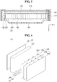
- FIGS. 4 and 5 are cross-sectional views illustrating a configuration of the optical sheet 125.
- the optical sheet 125 may be located in an upper portion of the bottom cover 130.
- the optical sheet 125 may be coupled to the bottom cover 130 at an edge of the bottom cover 130.
- the optical sheet 125 may be directly received at an edge of the bottom cover 130. That is, the optical sheet 125 may be supported by the bottom cover 130.
- An upper surface of an edge of the optical sheet 125 may be enclosed by a first guide panel 117.
- the optical sheet 125 may be located between an edge of the bottom cover 130 and a flange 117a of the first guide panel 117.
- the display panel 110 may be located. An edge of the display panel 110 may be coupled to the first guide panel 117. That is, the display panel 110 may be supported by the first guide panel 117.
- An edge area of the front surface of the display panel 110 may be enclosed by the front cover 105.
- the display panel 110 may be located between the first guide panel 117 and the front cover 105.
- the display device 100 may further include a second guide panel 113.
- the optical sheet 125 may be coupled to the second guide panel 113. That is, the second guide panel 113 may be coupled to the bottom cover 130, and the optical sheet 125 may be coupled to the second guide panel 113.
- the second guide panel 113 may be made of a material different from that of the bottom cover 130.
- the bottom cover 130 may enclose the first and second guide panels 117 and 113.
- the front cover 105 may not cover a front surface of the display panel 110. That is, one end portion of the front cover 105 may be located at a side surface of the display panel 110.
- the optical layer 123 may include a substrate 122, a reflection sheet 126, a light assembly 124, and a light guide plate 128.
- the optical layer 123 may be located on the bottom cover 130.
- the optical layer 123 may be located between the bottom cover 130 and the optical sheet 125.
- the optical layer 123 may be supported by the bottom cover 130.
- the substrate 122 may be located in at least one side of the inside of the bottom cover 130.
- the substrate 122 may be coupled to the first guide panel 117.
- the substrate 122 may be directly coupled to the first guide panel 117.
- the substrate 122 may be coupled to at least one of the first guide panel 117, the bottom cover 130, and the front cover 105.
- the substrate 122 may be located in a side surface direction of the reflection sheet 126 and/or the light guide plate 128. That is, a front surface of the substrate 122 may face toward the optical layer 123.
- the substrate 122 and the reflection sheet 126 and/or the light guide plate 128 may be separated by a predetermined gap. A detailed configuration of the substrate 122 and the optical layer 123 may be described in a corresponding portion.
- the backlight unit 120 may include a substrate 122, at least one light assembly 124, an optical layer 123 including the reflection sheet 126 and the light guide plate 128, and an optical sheet 125 located at the front surface side of the optical layer 123.
- the substrate 122 may be located in at least one side of another configuration of the optical layer 123.
- the substrate 122 may be extended in a direction orthogonal to a length direction of another configuration of the optical layer 123.
- At least one light assembly 124 may be mounted.
- an electrode pattern for connecting an adaptor and the light assembly 124 may be formed.
- a carbon nanotube electrode pattern for connecting the light assembly 124 and an adaptor may be formed.
- the substrate 122 may be made of at least one of polyethyleneterephthalate (PET), glass, polycarbonate (PC), and silicon.
- the substrate 122 may be a Printed Circuit Board (PCB) in which at least one light assembly 124 is mounted.
- PCB Printed Circuit Board
- the light assembly 124 may be disposed at a predetermined gap.
- a length direction width of the light assembly 124 may be smaller than a thickness direction width of the light guide plate 128. Therefore, most of light emitted from the light assembly 124 may be transferred to the inside of the light guide plate 128.
- the light assembly 124 may be a light emitting diode (LED) chip or a light emitting diode package including at least one LED chip.
- LED light emitting diode
- the light assembly 124 may be formed with a color LED that emits at least one of colors such as red, blue, and green or a white LED.
- the color LED may include at least one of red LED, blue LED, and green LED.
- a light source included in the light assembly 124 may be a Chip On Board (COB) type.
- the COB type light source may directly couple an LED chip, which is a light source to the substrate 122. Therefore, a process can be simplified. Further, resistance can be lowered and thus energy to be lost due to a heat can be reduced. That is, power efficiency of the light assembly 124 can be enhanced.
- the COB type light source can provide more bright lighting.
- the COB type light source may be implemented in a smaller thickness and a lighter weight than those of a conventional case.
- the light guide plate 128 may be located in an upper portion of the light assembly 124.
- the light guide plate 128 may perform a function of widely diffusing light applied from the light assembly 124.
- the light assembly 124 and an adjacent surface may be formed in a step shape.
- a lower surface of the light guide plate 128 is formed in a shape inclined upward to reflect light applied from the light assembly 124 upward.
- the reflection sheet 126 may be located at the rear surface side of the light guide plate 128.
- the reflection sheet 126 may reflect light emitted from the light assembly 124 to the front surface side.
- the reflection sheet 126 may reflect again light reflected from the light guide plate 128 to the front surface side.
- the reflection sheet 126 may include at least one of a metal and metal oxide, which is a reflection material.
- the reflection sheet 126 may include a metal and/or metal oxide having high reflectivity, such as at least one of aluminum (Al), silver (Ag), gold (Au), and titanium dioxide (TiO2).
- the reflection sheet 126 may be formed by depositing and/or coating a metal or metal oxide.
- ink including a metal material may be printed.
- a deposition layer using a vacuum deposition method such as a heat deposition method, an evaporation method, or a sputtering method may be formed.
- a coating layer and/or a print layer using a printing method, a gravure coating method, or a silk screen method may be formed.
- a diffusion plate (not shown) may be further included.
- the diffusion plate may diffuse light emitted from the light guide plate 128 to an upper portion.
- An air gap may be located between the light guide plate 128 and the optical sheet 125.
- the air gap may perform a buffer function of widely spreading light emitted from the light assembly 124.
- a resin may be deposited on the light assembly 124 and/or the reflection sheet 126. The resin may perform a function of diffusing lightemitted from the light assembly 124.
- the optical sheet 125 may be located at the front surface side of the light guide plate 128. A rear surface of the optical sheet 125 may close contact with the light guide plate 128, and a front surface of the optical sheet 125 may close contact with a rear surface of the display panel 110.
- the optical sheet 125 may include at least one sheet. Specifically, the optical sheet 125 may include at least one prism sheet and/or at least one diffusion sheet. A plurality of sheets included in the optical sheet 125 may be in a bonding state and/or a close contact state.
- the optical sheet 125 may be formed with a plurality of sheets having different functions.
- the optical sheet 125 may include first to three optical sheets 125a to 125c.
- the first optical sheet 125a may have a function of a diffusion sheet
- the second and third optical sheets 125b and 125c may have a function of a prism sheet.
- the number and/or a location of a diffusion sheet and a prism sheet may be changed.
- the optical sheet 125 may include the first optical sheet 125a, which is a diffusion sheet and the second optical sheet 125b, which is a prism sheet.
- the diffusion sheet prevents light emitted from the light guide plate 128 from partially concentrating, thereby more uniformly enabling luminance of light.
- the prism sheet concentrates light emitted from the diffusion sheet to enable light to be vertically applied to the display panel 110.
- the coupler 125d may be formed in at least one of corners of the optical sheet 125.
- the coupler 125d may be formed in at least one of the first to third optical sheets 125a to 125c.
- the coupler 125d may be formed at a corner of the long side of the optical sheet 125.
- the coupler 125d formed at the first long side and the coupler 125d formed at the second long side may be asymmetric. For example, a location and/or the number of the coupler 125d of the first long side and the coupler 125d of the second long side may be different.
- the substrate 122 and the light assembly 124 may be located in a direction of a lower side surface 110c of the display panel 110.
- a backlight unit in which the light assembly 124 is disposed at a side surface of the display panel 110 may be referred to as an edge type backlight unit.
- the light assembly 124 may emit light in a direction of an upper side surface 110d from the lower side surface 110c of the display panel 110. That is, light emitted from the light assembly 124 is diffused from the lower side surface 110c of the display panel 110 to the upper side surface 1 10d thereof to emit the entire display panel 110.
- a light emitting location of the light assembly 124 is not limited thereto and the light assembly 124 may be located at the upper side surface 110d of the display panel 110.
- the light assembly 124 may be located at a right side surface 110a of the display panel 110.
- a location of the light assembly 124 is not limited thereto and the light assembly 124 may be located at a left side surface 110b of the display panel 110.
- the light assembly 124 may be located at a lower side surface 110c and an upper side surface 110d of the display panel 110. As shown in FIG. 9C , the light assembly 124 may be located at the right side surface 110a and the left side surface 110b of the display panel 110.
- a backlight unit in which the light assemblies 124 are disposed at opposite both sides of the display panel 110 is referred to as a dual type backlight.
- the dual type backlight unit may enable light to be easily diffused to a front surface of the display panel 110 even to weaker light.
- the light assembly 124 may be located at a front surface of the display panel 110.
- the dual type backlight unit may diffuse light more easily than other backlight units.
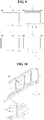
- FIGS. 10 to 12 are views illustrating a flange according to an exemplary embodiment of the present disclosure.
- a light arriving portion 230 may be provided.
- the bottom cover 130 may support an internal configuration of the display device 100.
- a configuration such as the backlight unit 120 may be coupled to the bottom cover 130.
- the bottom cover 130 may be made of a metal material.
- the bottom cover 130 may be made of aluminum alloy that can provide rigidity of a predetermined level or more while having a relatively light weight.
- various structures that can couple an internal configuration of the display device 100 may be added.
- a forming portion 248 and a light arriving portion 230 may be provided in the bottom cover 130.
- the forming portion 248 may be an area in which at least a partial area of the bottom cover 130 is protruded to the front side.
- the forming portion may also be referred to as a ribbed portion, a protruding portion, or the like.
- the forming portion 248 may be protrusions and depressions formed in at least a portion of a plate area 135 of the bottom cover 130 by a press processing.
- the forming portion 248 may perform a function of supporting the optical layer 123 received at an entire surface of a front surface of the bottom cover 130.
- the forming portion 248 may include first to three forming portions 245, 247, and 249.
- the first to three forming portions 245, 247, and 249 may be formed in parallel in a horizontal direction and/or a vertical direction of the bottom cover 130. Therefore, the optical layer 123 is supported by the first to three forming portions 245, 247, and 249 to enable a phenomenon such as a twist not to occur. That is, the first to three forming portions 245, 247, and 249 may stably support the optical layer 123 by a surface contact with the optical layer 123 at a plurality of points.
- the light arriving portion 230 may be formed in at least one corner area of the bottom cover 130.
- the light arriving portion 230 may also be referred to as a mounting portion or receiving portion for the backlight unit and/or light assembly and substrate.
- the light arriving portion 230 may include an arriving surface 220 (or planar surface) extended from the plate area 135 (or planar area) of the bottom cover 130 and a flange 210 in which the arriving surface 220 is extended and bent.
- the flange 210 may be formed in various forms.
- a plurality of flanges 210 are separated along a corner of the bottom cover 130 to be formed in a pair.
- first to three flanges 210a to 210c may be separated by a constant distance.
- D3 which is a distance from a central point of a corner of the bottom cover 130 in which the flange 210 is formed to the first flange 210a
- D2 which is a distance from a central point of a corner of the bottom cover 130 in which the flange 210 is formed to the second flange 210b
- D1 which is a distance from a central point of a corner of the bottom cover 130 in which the flange 210 is formed to the third flange 210c
- D1 may be smaller than D2 and/or D3. That is, at least a pair of the flange 210 is located adjacent to a central point to prevent the center of the substrate 122 coupled to the light arriving portion 230 from being drooped.
- the first flange 210a may be located at the outermost of a corner of both sides of the bottom cover 130. Due to the first flange 210a located at the outermost of the bottom cover 130, both ends of the substrate 122 coupled to the light arriving portion 230 can be prevented from being drooped.
- At least one of the flanges 210 may have a width different from that of at least another thereof.
- a width W1 of the first flange 210a may be larger than a width W2 of the second flange 210b and/or a width W3 of the third flange 210c. Therefore, both ends of the substrate 122 coupled to the light arriving portion 230 can be effectively prevented from being drooped.
- At least one of the flanges 210 may be different from that of at least another thereof.
- a height H1 of the first flange 210a may be larger than a height H2 of the second flange 210b and/or a height H3 of the third flange 210c.
- Such a form may be applied when an edge area has a thickness smaller than that of a central partial area in a design.
- one flange 210 may be continuously formed. That is, at the entire arriving surface 220 of the bottom cover 130, the flange 210 may be extended.
- FIGS. 13 to 21 are views illustrating a substrate according to an exemplary embodiment of the present disclosure.
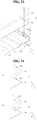
- the substrate 122 may include a first surface 122a in which a light source 124 is mounted and a second surface 122b bent from the first surface 122a.
- the substrate 122 may be formed in at least one of a PCB, a Flexible Printed Circuit Board(FPCB), and a Multilayer Printed Circuit Board (MPCB).
- FPCB Flexible Printed Circuit Board
- MPCB Multilayer Printed Circuit Board
- the light assembly 124 may be disposed at the first surface 122a.
- a plurality of light assemblies 124 may be disposed in parallel in a length direction of the first surface 122a.
- the light assembly 124 may include a light source and a lens located in an upper portion of the light source.
- the second surface 122b may be a portion in which the first surface 122a is extended.
- the second surface 122b may be a portion in which the first surface 122a is bent.
- the second surface 122b may be substantially orthogonally bent from the first surface 122a.
- a plurality of leads WI extended from the first surface 122a may be disposed.
- the plurality of leads WI may be extended to a connector area 122c.
- the connector area 122c may be located in at least one point of a corner of the second surface 122b.
- the connector area 122c may be a passage that connects the light assembly 124 of the first surface 122a to the outside. That is, a power source and/or a control signal necessary for operation of the light assembly 124 may be received from a controller and/or a power source of the display device 100 through the connector area 122c.
- the display device 100 may be designed to have a small thickness. This may be clearly understood in consideration that there is a limitation in reducing a thickness of a Z-direction due to a space necessary for the connector area 122c in a conventional plate-shaped substrate.
- the connector area 122c according to an exemplary embodiment of the present disclosure locates the connector area 122c at the second surface 122b unrelated to a thickness of the display device 100, thereby enhancing the degree of freedom of a design.
- a lead WI disposed at the second surface 122b may be concentrated.
- the connector area 122c may be coupled to the bottom cover 130.
- the connector area 122c may be coupled to the bottom cover 130, and the lead WI may be connected to the display device 100.
- the connector area 122c may be coupled to the bottom cover 130, and the substrate 122 may be fixed to the bottom cover 130.
- a width of the first surface 122a of the substrate 122 may be W5, and a length of the second surface 122b may be H5.
- the width W5 may be similar to a width L of the light assembly 124 mounted in the first surface 122a.
- the width W5 may be the same as or a little larger than the width L.
- the light assembly 124 mounted in the first surface 122a may be moved in a Z-direction, compared with a conventional case.
- the light assembly 124 may close contact with the second surface 122b side.
- the lead WI may be moved to the second surface 122b unlike a conventional case, a location of the light assembly 124 may be changed. That is, in a conventional substrate having a flat plate form, due to a space necessary for a disposition of a lead connected to the light assembly 124, there is a limitation in a location design of the light assembly 124.
- at least a portion of the lead WI may be moved to the second surface 122b. Therefore, a width of a Z-direction of the substrate 122 can be reduced and the degree of freedom of a location design of the light assembly 124 of the first surface 122a can be secured.
- the substrate 122 may be a small width W5, compared with when the substrate 122 is not formed with the first and second surfaces 122a and 122b. That is, in a conventional flat plate form, due to a disposition space of the lead WI and/or the connector area 122c, there is a limitation in reducing a size of the width W5. However, in the substrate 122 according to an exemplary embodiment of the present disclosure, by disposing the lead WI at the bent second surface 122b, the width W5 can be minimized. Therefore, the width W5 may be reduced to the same size as or to a size a little larger than the width L and thus a thickness of a Z-direction of the display device 100 can be reduced.
- the lead WI may be connected from the respective light assemblies 124 to the connector area 122c.
- a width W6 and a height H6 of the connector area 122c may be determined according to the number of the lead WI concentrated to the connector area 122c.
- the width W6 may increase according to a width of the lead WI and/or a distance between the leads WI. Therefore, the width W6 may increase in proportional to a size of the display device 100.
- the width W6 and/or the height H6 of the connector area 122c may be determined according to a bonding force necessary for coupling between the substrate 122 and the bottom cover 130. For example, when a larger fastening force is required, a size of the connector area 122c may be increased.
- the connector area 122c may be inserted into the coupler 135a formed in the bottom cover 130.
- the coupler 135a may have a form in which a partial area of the bottom cover 130 is cut out.
- a partial area of the bottom cover 130 may be in a state protruded in -Z-direction by a press processing.
- the coupler 135a may include an opening 135b formed in -Y-direction. A size of the opening 135b may be fixed in a state in which the substrate 122 is coupled to correspond to a size of the connector area 122c.
- the opening 135b is formed in the forming portion 248.
- the opening 135b is formed on the first forming portion 245 located at the lowermost of the bottom cover 130 so as to face the flange 210.
- a protruding portion 135c extended in a direction of the coupled connector area 122c may be formed.
- a lower end surface 245e of the first forming portion 245 may contact an upper end surface 122e of the substrate 122.
- the upper end surface 122e may naturally contact the lower end surface 245e. Therefore, by the lower end surface 245e, the substrate 122 may be guided to the arriving surface 220.
- the substrate 122 may be coupled to the light arriving portion 230 with a bonding method.
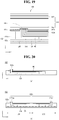
- an adhesive layer 295 may be located between the flange 210 of the light arriving portion 230 and the first surface 122a of the substrate 122.
- the adhesive layer 295 may be, for example, a double-sided tape. Therefore, the first surface 122a and the flange 210 may be fixed by a bonding force between the connector area 122c and the opening 135b and a bonding force by the adhesive layer 295.
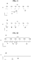
- FIGS. 20 and 21 illustrate a form of the connector area 122c according to various exemplary embodiments of the present disclosure.
- the connector area 122c may be located at one side of a corner of the substrate 122.
- a plurality of connector areas 122c may exist.
- the connector area 122c may include a first connector area 122ca located at one side of a corner of the substrate 122 and a second connector area 122cb located at the other side thereof.
- the first connector area 122ca may correspond to a first light assembly group LG1
- the second connector area 122cb may correspond to a second light assembly group LG2.
- an electronic component ED may be mounted at the second surface 122b.
- an electronic element ED necessary for operation of the light assembly 124 may be disposed. Therefore, while having no influence on a thickness of the display device 100, a necessary function can be effectively implemented.
- FIGS. 22 and 23 are views illustrating a heat releasing process of a substrate according to an exemplary embodiment of the present disclosure.
- the substrate 122 can more effectively release a heat that has occurred while operation of the light assembly 124.
- a heat may occur in the light assembly 124.
- the accumulated heat may have an influence on operation of the light assembly 124. Therefore, it is necessary to transfer a heat of the light assembly 124 to the bottom cover 130 made of a material having relatively high thermal conductivity.
- the substrate 122 Due to bending of the substrate 122, the substrate 122 according to an exemplary embodiment of the present disclosure may be coupled to the bottom cover 130. Thereby, a conventional housing structure necessary for coupling the substrate 122 to the bottom cover 130 may be omitted. Therefore, a heat of the substrate 122 may be more quickly and effectively conducted to the bottom cover 130 side.
- the flange 210 may be divided into a plurality of areas. For example, mutually separated first and second flanges 210a and 210b may exist. The first surface 122a of the substrate 122 may be exposed between the separated first and second flanges 210a and 210b. Therefore, a heat may be easily released to air through the exposed first surface 122a.
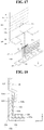
- FIGS. 24 to 46 are views illustrating a coupling structure according to an exemplary embodiment of the present disclosure.
- the display device 100 may couple the substrate 122 to the bottom cover 130 with various methods.
- the adhesive layer 295 may be located between the substrate 122 and the bottom cover 130.
- the adhesive layer 295 may be located between the second surface 122b of the substrate 122 and the arriving surface 220 of the bottom cover 130.
- the adhesive layer 295 may include first and second adhesive layers 295a and 295b.
- the first adhesive layer 295a may be located between the first surface 122a and the flange 210
- the second adhesive layer 295b may be located between the second surface 122b and the arriving surface 220.
- the adhesive layer 295 may be located in a partial area.
- a length of the first adhesive layer 295a is W6 and a length of the second adhesive layer 295b is H6
- a length W7 of the flange 210 and a length H7 of the arriving surface 220 may be larger than W6 and H6.
- the adhesive layer 295 may be an area fusion-bonded by a heat.
- the substrate 122 may be fixed to the bottom cover 130 using laser welding.
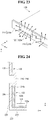
- the substrate 122 may be fixed to the bottom cover 130 using fastening members SC1 to SC3.
- the fastening members SC1 to SC3 may include first and second screws SC1 and SC2 coupling to the second surface 122b and the arriving surface 220 and/or the third screw SC3 coupling to the first surface 122a and the flange 210.
- the substrate 122 may directly contact the bottom cover 130 and thus enhancement of a heat conduction characteristic may be expected.
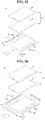
- the coupler 270 into which the substrate 122 is inserted may be formed.
- the coupler 270 may be formed in at least a partial area of the bottom cover 130.
- the coupler 270 may include a first coupler 270a and a second coupler 270b.
- the first coupler 270a may be located in an upper portion of the arriving surface 220, and the second coupler 270b may be located in an end portion of the flange 210.
- the first coupler 270a may be an opening formed in a portion of an upper portion of the arriving surface 220.
- the first coupler 270a may be provided in the first forming portion 245. A portion of an opening of the first coupler 270a may be shielded by the protruding portion 135c.
- a portion of an end portion of the flange 210 may be bent. That is, an end portion of the flange 210 may be a recess formed by bending a plurality of times in the same direction.
- the substrate 122 may be coupled to the bottom cover 130 by inserting into the coupler 270. That is, the first surface 122a may be inserted into the second coupler 270b, and the second surface 122b may be inserted into the first coupler 270a.
- a protruding portion 215 of a height H4 may be formed.
- the protruding portion 215 may enable the substrate 122 received in the flange 210 not to move in -Z-direction.
- a lower end surface 245e of the first forming portion 245 may enable the substrate 122 received in the flange 210 not to move in a Y-direction. Therefore, when a length A1 of the arriving surface 220 and a length A2 of the flange 210 correspond to a size of the substrate 122, the substrate 122 may be securely coupled to the light arriving portion 230.
- a coupling protrusion 260 may be protruded in -Z-direction.
- the coupling protrusion 260 may be coupled to the substrate 122.
- the coupling protrusion 260 may be inserted into a coupling hole formed in the second surface 122b.
- a plurality of coupling protrusions 260 may be protruded.
- a first coupling protrusion 260a may be protruded in a length W5 and a second coupling protrusion 260b may be protruded in a length W6.
- the second coupling protrusion 260b may be larger than the first coupling protrusion 260a.
- the first coupling protrusion 260a may correspond to a height of the second surface 122b of the substrate 122.
- the second coupling protrusion 260b may be protruded in -Z-direction further than a height of the second surface 122b of the substrate 122.
- the second coupling protrusion 260b may be protruded to the front side by passing through the second surface 122b.
- the second coupling protrusion 260b may be located between the light assemblies 124.
- a width D1 of the second coupling protrusion 260b may be smaller than a width D2 between the light assemblies 124. Therefore, light emitted from the light assembly 124 may not be disturbed by the protruded second coupling protrusion 260b.
- the first and second coupling holes 126a and 128a corresponding to the second coupling protrusion 260b may be formed. That is, in order to enable the second coupling protrusion 260b to be coupled and to enable to correspond to each second coupling protrusion 260b, the first and second coupling holes 126a and 128a may be located.
- a location of the optical layer 123 may be fixed to an initial design location.
- a distance between the optical layer 123 and the light assembly 124 may be fixed to a design location.
- one side of the first and second coupling holes 126a and 128a may be opened at a corner of the reflection sheet 126 and the light guide plate 128.
- the first and second coupling holes 126a and 128a may be formed in an area of the inside of the reflection sheet 126 and the light guide plate 128.
- the first coupling hole 126a is provided in a through-hole form
- the second coupling hole 128a may be formed in a depth smaller than a thickness of the light guide plate 128. That is, the second coupling protrusion 260b may not penetrate the light guide plate 128.
- the substrate 122 in which the light assembly 124 is mounted may be located at a corner of both sides of the display device 100. That is, two substrates 122 may be located at an opposite location.
- the coupling protrusion 260 may be located to correspond to each corner area of the bottom cover 130.
- first and second coupling protrusions 260a and 260b may be each provided.
- first and second coupling holes 126a and 128a corresponding to the second coupling protrusion 260b having a long length may be formed.
- a side cover 107 may be located at a side surface of the bottom cover 130.
- the side cover 107 may have a form in which the bottom cover 130 is extended.
- at least one corner of four corners of the bottom cover 130 is bent to form the side cover 107.
- the side cover 107 may be formed integrally with the bottom cover 130 rather than a separate structure.
- the side cover 107 is formed separately from the bottom cover 130 to be coupled to the bottom cover 130.
- the substrate 122 in which the light assembly 124 is mounted may be located at each corner of the display device 100. Accordingly, the coupling protrusion 260 may be located to correspond to each corner area of the bottom cover 130. In the reflection sheet 126 and the light guide plate 128, a first coupling hole 126a corresponding to the coupling protrusion 260b may be formed.
- the second coupling protrusion 260b may be located in a corner area of the bottom cover 130.
- the second coupling protrusion 260b may be formed.
- the first coupling hole 126a may be formed. That is, at a corner of the reflection sheet 126 and the light guide plate 128, the first coupling hole 126a of a form in which two surfaces are opened may be formed.
- the second coupling protrusion 260b may be located in each corner area of the bottom cover 130. Even in each corner of the reflection sheet 126 and the light guide plate 128, the first coupling hole 126a may be formed.
- the substrate 122 in which the light assembly 124 is provided may be disposed along one corner of the display device 100.
- the substrate 122 may be disposed along the long side of the lower side.
- a third coupling hole 260c may be protruded from the bottom cover 130.
- the third coupling hole 260c may be protruded from the bottom cover 130 of the short side of the display device 100.
- the third coupling hole 260c may fix the optical layer 123 to a specific location.
- the third coupling hole 260c is inserted into a third coupling hole 128c of a side surface of the light guide plate 128 to prevent the light guide plate 128 from moving.
- the third coupling hole 260c may be located at both short sides and/or long sides. At the long side of the lower side to which a load is relatively applied, a plurality of third coupling holes 260c may be located.
- fourth and fifth coupling protrusions 260d and 260e may be formed in the bottom cover 130.
- the fourth coupling protrusion 260d may be protruded
- the fifth coupling protrusion 260e may be protruded.
- the substrate 122 may be coupled to the fourth and fifth coupling protrusions 260d and 260e.
- the fourth coupling protrusion 260d may contact the optical layer 123 at a side surface of the optical layer 123. That is, the fourth coupling protrusion 260d may support the optical layer 123 in a Y-direction.
- the fourth coupling protrusion 260d may be separately disposed in the plural along the substrate 122.
- the fourth coupling protrusion 260d may constantly maintain a gap between the optical layer 123 and the light assembly 124.
- a fourth coupling hole 128d corresponding to the fourth coupling protrusion 260d may be formed.
- the fourth coupling hole 128d may be formed at a corner of the light guide plate 128, the fourth coupling hole 128d may be formed.
- the fifth coupling protrusion 107a contacting the optical layer 123 may be formed.
- the fifth coupling protrusion 107a may be located at a corner different from that of the fourth coupling protrusion 260d.
- the fifth coupling protrusion 107a may be located at the short side of the display device 100.
- the fifth coupling protrusion 107a may be protruded from the side cover 107.
- the fifth coupling protrusion 107a may be protruded from the bottom cover 130.
- the fifth coupling protrusion 107a may be provided at a corner other than a corner in which the substrate 122 is located. That is, at both short sides of the display device 100, the fifth coupling protrusion 107a is provided to support the optical layer 123.
- the fifth coupling protrusion 107a may be provided at an opposite location of both sides of a corner of the short side.
- the fifth coupling protrusion 107a may be located at an area other than a corner in which the substrate 122 is located.
- the fifth coupling protrusion 107a of FIG. 45 is different from the fifth coupling protrusion 107a of FIG. 44 asymmetrically disposed at both sides of a corner of the short side.
- a coupling groove 217 may be formed in the bottom cover 130.
- the coupling groove 217 may be located in an area corresponding to the flange 210.
- the coupling groove 217 may have a form in which a portion of a corner area in which the flange 210 and the arriving portion 220 contact is removed.
- the coupling groove 217 may be coupled to a coupler 122f formed in the substrate 122. By coupling the coupling groove 217 and the coupler 122f, the substrate 122 may be fixed to the bottom cover 130.
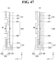
- FIG. 47 is a diagram illustrating a forming structure according to an exemplary embodiment of the present disclosure.
- the display device 100 may change a shape of the forming portion 248 to correspond to a necessary location of the optical layer 123.
- the optical layer 123 may be received in the forming portion 248.
- the reflection sheet 126 may directly contact and the light guide plate 128 may be located thereon.
- a height of the forming portion 248 may correspond to a necessary location of the optical layer 123.
- a height of the forming portion 248 may be changed according to a size of the display device 100, a characteristic of the light assembly 124, and a characteristic of the optical layer 123.
- the display device 100 may form a height of the forming portion 248 in W5, as shown in FIG. 47A or may form a height of the forming portion 248 in W6, as shown in FIG. 47B .
- the optical layer 123 may be raised to a location thereof. More conveniently, a location of the optical layer 123 and/or a location of the light assembly 124 may be designed.
- a height of the forming portion 248 may correspond to a location of the light assembly 124.
- a height of the forming portion 248 may be changed according to a case in which the light assembly 124 is relatively leaned in -Z-direction and an opposite case. Therefore, the degree of freedom of a design can be easily secured.
Landscapes
- Physics & Mathematics (AREA)
- Nonlinear Science (AREA)
- General Physics & Mathematics (AREA)
- Optics & Photonics (AREA)
- Mathematical Physics (AREA)
- Chemical & Material Sciences (AREA)
- Crystallography & Structural Chemistry (AREA)
- Liquid Crystal (AREA)
- Planar Illumination Modules (AREA)
- Devices For Indicating Variable Information By Combining Individual Elements (AREA)
Description
- This application claims the benefit of earlier filing date and right of priority to Korean Patent Application No.
10-2014-0195644, filed on Dec. 31, 2014 - The present disclosure relates to a backlight unit including a bent substrate and a display device including the same.
- With the development of the information society, various demands for display devices have been increasing. Various display devices, such as liquid crystal displays (LCDs), plasma display panels (PDPs), electroluminescent displays (ELDs), and vacuum fluorescent displays (VFDs), have been recently studied and used to meet various demands for the display devices. Among the display devices, a liquid crystal display panel of the liquid crystal display includes a liquid crystal layer, and a thin film transistor (TFT) substrate and a color filter substrate which are positioned opposite each other with the liquid crystal layer interposed there between. The liquid crystal display panel displays an image using light provided by a backlight unit of the liquid crystal display.
-
US 2012/026424 A1 describes a liquid crystal display device. The liquid crystal display device includes a liquid crystal panel, a backlight unit, a main frame, a top frame and a bottom frame. The liquid crystal panel and the backlight unit are surrounded and integrated by the main frame, the top frame and the bottom frame. A LED assembly disposed on a side of the light guide plate includes a plurality of LEDs and an LED printed circuit board where the plurality of LEDs is disposed. -
US 2009/116262 A1 describes a display device comprising a housing, a light guide member, a diffusion sheet, a prism sheet, a reflection sheet, a light-emitting module, and a liquid crystal panel. The light-emitting module comprises light-emitting devices, a board, and a metal plate. - The objects of the present invention are solved by the features of the independent claim. Preferred embodiments of the present invention provides a display device according to the dependent claims.
- The accompanying drawings, which are included to provide a further understanding of the disclosure and are incorporated in and constitute a part of this application, illustrate embodiment(s) of the disclosure and together with the description serve to explain the principle of the disclosure.
-
FIGS. 1 and 2 are perspective views illustrating a display device according to an exemplary embodiment of the present disclosure; -
FIGS. 3 to 9 are views illustrating a configuration of a display device according to an exemplary embodiment of the present disclosure; -
FIGS. 10 to 12 are views illustrating a flange according to an exemplary embodiment of the present disclosure; -
FIGS. 13 to 21 are views illustrating a substrate according to an exemplary embodiment of the present disclosure; -
FIGS. 22 and23 are views illustrating a heat releasing process of a substrate according to an exemplary embodiment of the present disclosure; -
FIGS. 24 to 46 are views illustrating a coupling structure according to an exemplary embodiment of the present disclosure; and -
FIG. 47 is a cross-sectional view illustrating a forming structure according to an exemplary embodiment of the present disclosure. - Arrangements and embodiments may now be described more fully with reference to the accompanying drawings, in which exemplary embodiments may be shown. Embodiments may, however, be embodied in many different forms and should not be construed as being limited to embodiments set forth herein; rather, embodiments may be provided so that this disclosure will be thorough and complete, and will fully convey the concept to those skilled in the art.
- A display device may be described below with reference to the accompanying drawings. In the following description, suffixes "module" and "unit" may be given to components of the mobile terminal in consideration of only facilitation of description and do not have meanings or functions discriminated from each other.
- The terms 'first', 'second', etc., may be used to describe various components, but the components are not limited by such terms. The terms are used only for the purpose of distinguishing one component from other components. For example, a first component may be designated as a second component without departing from the scope of the present disclosure. In the same manner, the second component may be designated as the first component.
- The term "and/or" encompasses both combinations of the plurality of related items disclosed and any item from among the plurality of related items disclosed.
- When an arbitrary component is described as "being connected to "or" being linked to" another component, this should be understood to mean that still another component(s) may exist between them, although the arbitrary component may be directly connected to, or linked to, the second component. In contrast, when an arbitrary component is described as "being directly connected to" or "being directly linked to" another component, this should be understood to mean that no component exists between them.
- The terms used in the present application are used to describe only specific embodiments or examples, and are not intended to limit the present disclosure. A singular expression can include a plural expression as long as it does not have an apparently different meaning in context.
- In the present application, the terms "include" and "have" should be understood to be intended to designate that illustrated features, numbers, steps, operations, components, parts or combinations thereof exist and not to preclude the existence of one or more different features, numbers, steps, operations, components, parts or combinations thereof, or the possibility of the addition thereof.
- Unless otherwise specified, all of the terms which are used herein, including the technical or scientific terms, have the same meanings as those that are generally understood by a person having ordinary knowledge in the art to which the present disclosure pertains. The terms defined in a generally used dictionary must be understood to have meanings identical to those used in the context of a related art, and are not to be construed to have ideal or excessively formal meanings unless they are obviously specified in the present application.
- The following exemplary embodiments of the present disclosure are provided to those skilled in the art in order to describe the present disclosure more completely. Accordingly, shapes and sizes of elements shown in the drawings may be exaggerated for clarity.
- Hereinafter, a liquid crystal display panel is used as an example of a display panel. Other display panels may be used.
- Hereinafter, a
display panel 110 may include a First Long Side (LS1), a Second Long Side (LS2) opposite to the LS1, a First Short Side (SSI) adjacent to the LS1 and the LS2, and a Second Short Side (SS2) opposite to the SS1. - Here, the SS1 may be referred to as a first side area, the SS2 may be referred to as a second side area opposite to the first side area, the LS1 may be referred to as a third side area adjacent to the first side area and the second side area and located between the first side area and the second side area, and the LS2 may be referred to as a fourth side area adjacent to the first side area and the second side area, located between the first side area and the second side area, and opposite to the third side area.
- Further, for convenience of description, it is described that a length of the LS1 and LS2 is longer than that of the SS1 and SS2, but a length of the LS1 and LS2 may be approximately the same as that of the SS1 and SS2.
- Hereinafter, a First Direction (DR1) may be a direction parallel to the LS1 and LS2 of the
display panel 100, and a Second Direction (DR2) may be a direction parallel to the SS1 and SS2 of thedisplay panel 110. - A Third Direction (DR3) may be a direction vertical to the DR1 and/or the DR2.
- The DR1 and the DR2 may be referred to as a horizontal direction.
- Further, the DR3 may be referred to as a vertical direction.
-
FIGS. 1 and 2 are perspective views illustrating a display device according to an exemplary embodiment of the present disclosure. - As shown in
FIGS. 1 and 2 , adisplay device 100 according to an exemplary embodiment of the present disclosure may include adisplay panel 110 and aback cover 150 of the rear side of thedisplay panel 110. - The
back cover 150 may be connected to thedisplay panel 110 with a sliding method in a direction from the LS1 toward the LS2, i.e., in the DR2. In other words, theback cover 150 may be inserted with a sliding method from the SS1 of thedisplay panel 110, the SS2 opposite to the SS1, and the LS1 adjacent to the SS1 and SS2 and located between the SS1 and the SS2. - In order to connect the
back cover 150 to thedisplay panel 110 with a sliding method, theback cover 150 and/or other structures adjacent thereto may include a protruding portion, a sliding portion, and a coupler. -
FIGS. 3 to 7 are views illustrating a configuration of a display device according to an exemplary embodiment of the present disclosure. - As shown in
FIG. 3 , thedisplay device 100 according to an exemplary embodiment of the present disclosure may include afront cover 105, adisplay panel 110, abacklight unit 120, abottom cover 130, and aback cover 150. - The
front cover 105 may cover at least a partial area of a front surface and a side surface of thedisplay panel 110. Thefront cover 105 may have a quadrangular frame shape having the hollow center. Because thefront cover 105 has the hollow center, an image of thedisplay panel 110 may be displayed to the outside. - The
front cover 105 may be divided into a front surface cover and a side surface cover. That is, thefront cover 105 may be divided into a front surface cover located at the front surface side of thedisplay panel 110 and a side surface cover located at the side surface side of thedisplay panel 110. The front surface cover and the side surface cover may be separately formed. Any one of the front surface cover and the side surface cover may be omitted. For example, for an object of an enhanced design, the front surface cover may not exist and only a side surface cover may exist. - The
display panel 110 is provided at a front surface of thedisplay device 100 and may display an image. Thedisplay panel 110 may divide an image into a plurality of pixels to output an image by adjusting color, brightness, and chroma per pixel. Thedisplay panel 110 may be divided into an active area that displays an image and an inactive area that does not displayan image. Thedisplay panel 110 may include an opposing front substrate and rear substrate with a liquid crystal layer interposed therebetween. - The front substrate may include a plurality of pixels consisting of red (R), green (G), and blue (B) subpixels. The front substrate may generate an image corresponding to a color of red, green, or blue according to a control signal.
- The rear substrate may include switching elements. The rear substrate may switch a pixel electrode. For example, the pixel electrode may change molecule arrangement of a liquid crystal layer according to a control signal applied from the outside. The liquid crystal layer may include a plurality of liquid crystal molecules. The liquid crystal molecules may change arrangement to correspond to a voltage difference occurring between a pixel electrode and a common electrode. The liquid crystal layer may transfer light provided from the
backlight unit 120 to the front substrate. - The
backlight unit 120 may be located at the rear surface side of thedisplay panel 110. Thebacklight unit 120 may include a plurality of light sources. A light source of thebacklight unit 120 may be disposed in a direct type or an edge type. When thebacklight unit 120 is a directtype backlight unit 120, a diffusion plate may be further included. - The
backlight unit 120 may be coupled to a front surface and a surface side of thebottom cover 130. For example, a plurality of light sources may be disposed at the inside of one side of thebottom cover 130, and this may be referred to as an edge type backlight unit. - The
backlight unit 120 may be driven with an entire driving method or a partial driving method such as local dimming and impulsive. Thebacklight unit 120 may include anoptical sheet 125 and anoptical layer 123. - The
optical sheet 125 may enable light of a light source to be uniformly transferred to thedisplay panel 110. Theoptical sheet 125 may be formed with a plurality of layers. For example, theoptical sheet 125 may include at least one prism sheet and/or at least one diffusion sheet. - In the
optical sheet 125, at least onecoupler 125d may exist. Thecoupler 125d may be coupled to thefront cover 105 and/or theback cover 150. That is, thecoupler 125d may be directly coupled to thefront cover 105 and/or theback cover 150. Alternatively, thecoupler 125d may be coupled to a structure coupled onto thefront cover 105 and/or theback cover 150. That is, thecoupler 125d may be indirectly coupled to thefront cover 105 and/or theback cover 150. - The
optical layer 123 may include a light source. A detailed configuration of theoptical layer 123 will be described in a corresponding portion. - The
bottom cover 130 may perform a function of supporting constituent elements of thedisplay device 100. For example, a configuration of thebacklight unit 120 may be coupled to thebottom cover 130. Thebottom cover 130 may be made of a metal material such as an aluminum alloy. Thebottom cover 130 may be referred to as a frame. - The
back cover 150 may be located at a rear surface of thedisplay device 100. Theback cover 150 may protect an internal configuration from the outside. At least a portion of theback cover 150 may be coupled to thebottom cover 130 and/or thefront cover 105. Theback cover 150 may be an injection material made of a resin material. -
FIGS. 4 and5 are cross-sectional views illustrating a configuration of theoptical sheet 125. - As shown in
FIG. 4A , in an upper portion of thebottom cover 130, theoptical sheet 125 may be located. Theoptical sheet 125 may be coupled to thebottom cover 130 at an edge of thebottom cover 130. Theoptical sheet 125 may be directly received at an edge of thebottom cover 130. That is, theoptical sheet 125 may be supported by thebottom cover 130. An upper surface of an edge of theoptical sheet 125 may be enclosed by afirst guide panel 117. For example, theoptical sheet 125 may be located between an edge of thebottom cover 130 and aflange 117a of thefirst guide panel 117. - At the front surface side of the
optical sheet 125, thedisplay panel 110 may be located. An edge of thedisplay panel 110 may be coupled to thefirst guide panel 117. That is, thedisplay panel 110 may be supported by thefirst guide panel 117. - An edge area of the front surface of the
display panel 110 may be enclosed by thefront cover 105. For example, thedisplay panel 110 may be located between thefirst guide panel 117 and thefront cover 105. - As shown in
FIG. 4B , thedisplay device 100 according to an exemplary embodiment of the present disclosure may further include asecond guide panel 113. Theoptical sheet 125 may be coupled to thesecond guide panel 113. That is, thesecond guide panel 113 may be coupled to thebottom cover 130, and theoptical sheet 125 may be coupled to thesecond guide panel 113. Thesecond guide panel 113 may be made of a material different from that of thebottom cover 130. Thebottom cover 130 may enclose the first andsecond guide panels - As shown in
FIG. 4C , in thedisplay device 100 according to an exemplary embodiment of the present disclosure, thefront cover 105 may not cover a front surface of thedisplay panel 110. That is, one end portion of thefront cover 105 may be located at a side surface of thedisplay panel 110. - As shown in
FIG. 5 , theoptical layer 123 may include asubstrate 122, areflection sheet 126, alight assembly 124, and alight guide plate 128. - The
optical layer 123 may be located on thebottom cover 130. For example, theoptical layer 123 may be located between thebottom cover 130 and theoptical sheet 125. Theoptical layer 123 may be supported by thebottom cover 130. - The
substrate 122 may be located in at least one side of the inside of thebottom cover 130. Thesubstrate 122 may be coupled to thefirst guide panel 117. Thesubstrate 122 may be directly coupled to thefirst guide panel 117. For example, thesubstrate 122 may be coupled to at least one of thefirst guide panel 117, thebottom cover 130, and thefront cover 105. - The
substrate 122 may be located in a side surface direction of thereflection sheet 126 and/or thelight guide plate 128. That is, a front surface of thesubstrate 122 may face toward theoptical layer 123. Thesubstrate 122 and thereflection sheet 126 and/or thelight guide plate 128 may be separated by a predetermined gap. A detailed configuration of thesubstrate 122 and theoptical layer 123 may be described in a corresponding portion. - Referring to
FIGS. 6 and7 , thebacklight unit 120 may include asubstrate 122, at least onelight assembly 124, anoptical layer 123 including thereflection sheet 126 and thelight guide plate 128, and anoptical sheet 125 located at the front surface side of theoptical layer 123. - The
substrate 122 may be located in at least one side of another configuration of theoptical layer 123. Thesubstrate 122 may be extended in a direction orthogonal to a length direction of another configuration of theoptical layer 123. - In the
substrate 122, at least onelight assembly 124 may be mounted. In thesubstrate 122, an electrode pattern for connecting an adaptor and thelight assembly 124 may be formed. For example, in thesubstrate 122, a carbon nanotube electrode pattern for connecting thelight assembly 124 and an adaptor may be formed. - The
substrate 122 may be made of at least one of polyethyleneterephthalate (PET), glass, polycarbonate (PC), and silicon. Thesubstrate 122 may be a Printed Circuit Board (PCB) in which at least onelight assembly 124 is mounted. - In the
substrate 122, thelight assembly 124 may be disposed at a predetermined gap. A length direction width of thelight assembly 124 may be smaller than a thickness direction width of thelight guide plate 128. Therefore, most of light emitted from thelight assembly 124 may be transferred to the inside of thelight guide plate 128. - The
light assembly 124 may be a light emitting diode (LED) chip or a light emitting diode package including at least one LED chip. - The
light assembly 124 may be formed with a color LED that emits at least one of colors such as red, blue, and green or a white LED. The color LED may include at least one of red LED, blue LED, and green LED. - A light source included in the
light assembly 124 may be a Chip On Board (COB) type. The COB type light source may directly couple an LED chip, which is a light source to thesubstrate 122. Therefore, a process can be simplified. Further, resistance can be lowered and thus energy to be lost due to a heat can be reduced. That is, power efficiency of thelight assembly 124 can be enhanced. The COB type light source can provide more bright lighting. The COB type light source may be implemented in a smaller thickness and a lighter weight than those of a conventional case. - The
light guide plate 128 may be located in an upper portion of thelight assembly 124. Thelight guide plate 128 may perform a function of widely diffusing light applied from thelight assembly 124. Although not shown, in thelight guide plate 128, thelight assembly 124 and an adjacent surface may be formed in a step shape. A lower surface of thelight guide plate 128 is formed in a shape inclined upward to reflect light applied from thelight assembly 124 upward. - The
reflection sheet 126 may be located at the rear surface side of thelight guide plate 128. Thereflection sheet 126 may reflect light emitted from thelight assembly 124 to the front surface side. Thereflection sheet 126 may reflect again light reflected from thelight guide plate 128 to the front surface side. - The
reflection sheet 126 may include at least one of a metal and metal oxide, which is a reflection material. For example, thereflection sheet 126 may include a metal and/or metal oxide having high reflectivity, such as at least one of aluminum (Al), silver (Ag), gold (Au), and titanium dioxide (TiO2). - The
reflection sheet 126 may be formed by depositing and/or coating a metal or metal oxide. In thereflection sheet 126, ink including a metal material may be printed. In thereflection sheet 126, a deposition layer using a vacuum deposition method such as a heat deposition method, an evaporation method, or a sputtering method may be formed. In thereflection sheet 126, a coating layer and/or a print layer using a printing method, a gravure coating method, or a silk screen method may be formed. - At front surface side of the
light guide plate 128, a diffusion plate (not shown) may be further included. The diffusion plate may diffuse light emitted from thelight guide plate 128 to an upper portion. - An air gap may be located between the
light guide plate 128 and theoptical sheet 125. The air gap may performa buffer function of widely spreading light emitted from thelight assembly 124. A resin may be deposited on thelight assembly 124 and/or thereflection sheet 126. The resin may performa function of diffusing lightemitted from thelight assembly 124. - The
optical sheet 125 may be located at the front surface side of thelight guide plate 128. A rear surface of theoptical sheet 125 may close contact with thelight guide plate 128, and a front surface of theoptical sheet 125 may close contact with a rear surface of thedisplay panel 110. - The
optical sheet 125 may include at least one sheet. Specifically, theoptical sheet 125 may include at least one prism sheet and/or at least one diffusion sheet. A plurality of sheets included in theoptical sheet 125 may be in a bonding state and/or a close contact state. - The
optical sheet 125 may be formed with a plurality of sheets having different functions. For example, theoptical sheet 125 may include first to threeoptical sheets 125a to 125c. The firstoptical sheet 125a may have a function of a diffusion sheet, and the second and thirdoptical sheets optical sheet 125 may include the firstoptical sheet 125a, which is a diffusion sheet and the secondoptical sheet 125b, which is a prism sheet. - The diffusion sheet prevents light emitted from the
light guide plate 128 from partially concentrating, thereby more uniformly enabling luminance of light. The prism sheet concentrates light emitted from the diffusion sheet to enable light to be vertically applied to thedisplay panel 110. - The
coupler 125d may be formed in at least one of corners of theoptical sheet 125. Thecoupler 125d may be formed in at least one of the first to thirdoptical sheets 125a to 125c. - The
coupler 125d may be formed at a corner of the long side of theoptical sheet 125. Thecoupler 125d formed at the first long side and thecoupler 125d formed at the second long side may be asymmetric. For example, a location and/or the number of thecoupler 125d of the first long side and thecoupler 125d of the second long side may be different. - Referring to
FIGS. 8 and9 , thesubstrate 122 and thelight assembly 124 may be located in a direction of alower side surface 110c of thedisplay panel 110. A backlight unit in which thelight assembly 124 is disposed at a side surface of thedisplay panel 110 may be referred to as an edge type backlight unit. - As shown in
FIG. 8 , thelight assembly 124 may emit light in a direction of anupper side surface 110d from thelower side surface 110c of thedisplay panel 110. That is, light emitted from thelight assembly 124 is diffused from thelower side surface 110c of thedisplay panel 110 to theupper side surface 1 10d thereof to emit theentire display panel 110. However, a light emitting location of thelight assembly 124 is not limited thereto and thelight assembly 124 may be located at theupper side surface 110d of thedisplay panel 110. - As shown in
FIG. 9A , thelight assembly 124 may be located at aright side surface 110a of thedisplay panel 110. However, a location of thelight assembly 124 is not limited thereto and thelight assembly 124 may be located at aleft side surface 110b of thedisplay panel 110. - As shown in
FIG. 9B , thelight assembly 124 may be located at alower side surface 110c and anupper side surface 110d of thedisplay panel 110. As shown inFIG. 9C , thelight assembly 124 may be located at theright side surface 110a and theleft side surface 110b of thedisplay panel 110. - As shown in
FIGS. 9B and 9C , a backlight unit in which thelight assemblies 124 are disposed at opposite both sides of thedisplay panel 110 is referred to as a dual type backlight. The dual type backlight unit may enable light to be easily diffused to a front surface of thedisplay panel 110 even to weaker light. - As shown in
FIG. 9D , thelight assembly 124 may be located at a front surface of thedisplay panel 110. When thelight assembly 124 is located at a front surface of thedisplay panel 110, the dual type backlight unit may diffuse light more easily than other backlight units. -
FIGS. 10 to 12 are views illustrating a flange according to an exemplary embodiment of the present disclosure. - As shown in
FIGS. 10 to 12 , in at least one corner of thebottom cover 130 according to an exemplary embodiment of the present disclosure, alight arriving portion 230 may be provided. - As shown in
FIG. 10 , thebottom cover 130 may support an internal configuration of thedisplay device 100. For example, as described above, a configuration such as thebacklight unit 120 may be coupled to thebottom cover 130. - The
bottom cover 130 may be made of a metal material. For example, thebottom cover 130 may be made of aluminum alloy that can provide rigidity of a predetermined level or more while having a relatively light weight. In thebottom cover 130, various structures that can couple an internal configuration of thedisplay device 100 may be added. For example, in thebottom cover 130, a formingportion 248 and alight arriving portion 230 may be provided. - The forming
portion 248 may be an area in which at least a partial area of thebottom cover 130 is protruded to the front side. The forming portion may also be referred to as a ribbed portion, a protruding portion, or the like. For example, the formingportion 248 may be protrusions and depressions formed in at least a portion of aplate area 135 of thebottom cover 130 by a press processing. - The forming
portion 248 may perform a function of supporting theoptical layer 123 received at an entire surface of a front surface of thebottom cover 130. The formingportion 248 may include first to three formingportions portions bottom cover 130. Therefore, theoptical layer 123 is supported by the first to three formingportions portions optical layer 123 by a surface contact with theoptical layer 123 at a plurality of points. - The
light arriving portion 230 may be formed in at least one corner area of thebottom cover 130. Thelight arriving portion 230 may also be referred to as a mounting portion or receiving portion for the backlight unit and/or light assembly and substrate. Thelight arriving portion 230 may include an arriving surface 220 (or planar surface) extended from the plate area 135 (or planar area) of thebottom cover 130 and aflange 210 in which the arrivingsurface 220 is extended and bent. - As shown in
FIGS. 11 and 12 , theflange 210 may be formed in various forms. - As shown in
FIG. 11A , a plurality offlanges 210 are separated along a corner of thebottom cover 130 to be formed in a pair. For example, first to threeflanges 210a to 210c may be separated by a constant distance. - Distances between at least two of the first to three
flanges 210a to 210c may be different. At least one of D3, which is a distance from a central point of a corner of thebottom cover 130 in which theflange 210 is formed to thefirst flange 210a, D2, which is a distance from a central point of a corner of thebottom cover 130 in which theflange 210 is formed to thesecond flange 210b, and D1, which is a distance from a central point of a corner of thebottom cover 130 in which theflange 210 is formed to thethird flange 210c may be different. For example, D1 may be smaller than D2 and/or D3. That is, at least a pair of theflange 210 is located adjacent to a central point to prevent the center of thesubstrate 122 coupled to thelight arriving portion 230 from being drooped. - The
first flange 210a may be located at the outermost of a corner of both sides of thebottom cover 130. Due to thefirst flange 210a located at the outermost of thebottom cover 130, both ends of thesubstrate 122 coupled to thelight arriving portion 230 can be prevented from being drooped. - As shown in
FIG. 11B , at least one of theflanges 210 may have a width different from that of at least another thereof. For example, a width W1 of thefirst flange 210a may be larger than a width W2 of thesecond flange 210b and/or a width W3 of thethird flange 210c. Therefore, both ends of thesubstrate 122 coupled to thelight arriving portion 230 can be effectively prevented from being drooped. - As shown in
FIG. 12A , at least one of theflanges 210 may be different from that of at least another thereof. For example, a height H1 of thefirst flange 210a may be larger than a height H2 of thesecond flange 210b and/or a height H3 of thethird flange 210c. Such a form may be applied when an edge area has a thickness smaller than that of a central partial area in a design. - As shown in
FIG. 12B , oneflange 210 may be continuously formed. That is, at the entire arrivingsurface 220 of thebottom cover 130, theflange 210 may be extended. -
FIGS. 13 to 21 are views illustrating a substrate according to an exemplary embodiment of the present disclosure. - As shown in
FIGS. 13 to 21 , thesubstrate 122 according to an exemplary embodiment of the present disclosure may include afirst surface 122a in which alight source 124 is mounted and asecond surface 122b bent from thefirst surface 122a. Thesubstrate 122 may be formed in at least one of a PCB, a Flexible Printed Circuit Board(FPCB), and a Multilayer Printed Circuit Board (MPCB). - As shown in
FIG. 13A , at thefirst surface 122a, thelight assembly 124 may be disposed. A plurality oflight assemblies 124 may be disposed in parallel in a length direction of thefirst surface 122a. Thelight assembly 124 may include a light source and a lens located in an upper portion of the light source. - The
second surface 122b may be a portion in which thefirst surface 122a is extended. Thesecond surface 122b may be a portion in which thefirst surface 122a is bent. Thesecond surface 122b may be substantially orthogonally bent from thefirst surface 122a. At thesecond surface 122b, a plurality of leads WI extended from thefirst surface 122a may be disposed. The plurality of leads WI may be extended to aconnector area 122c. - The
connector area 122c may be located in at least one point of a corner of thesecond surface 122b. Theconnector area 122c may be a passage that connects thelight assembly 124 of thefirst surface 122a to the outside. That is, a power source and/or a control signal necessary for operation of thelight assembly 124 may be received from a controller and/or a power source of thedisplay device 100 through theconnector area 122c. - As the
connector area 122c is located at thesecond surface 122b, thedisplay device 100 may be designed to have a small thickness. This may be clearly understood in consideration that there is a limitation in reducing a thickness of a Z-direction due to a space necessary for theconnector area 122c in a conventional plate-shaped substrate. Theconnector area 122c according to an exemplary embodiment of the present disclosure locates theconnector area 122c at thesecond surface 122b unrelated to a thickness of thedisplay device 100, thereby enhancing the degree of freedom of a design. - In the
connector area 122c, a lead WI disposed at thesecond surface 122b may be concentrated. Theconnector area 122c may be coupled to thebottom cover 130. Theconnector area 122c may be coupled to thebottom cover 130, and the lead WI may be connected to thedisplay device 100. Theconnector area 122c may be coupled to thebottom cover 130, and thesubstrate 122 may be fixed to thebottom cover 130. - As shown in
FIG. 13B , a width of thefirst surface 122a of thesubstrate 122 may be W5, and a length of thesecond surface 122b may be H5. The width W5 may be similar to a width L of thelight assembly 124 mounted in thefirst surface 122a. For example, the width W5 may be the same as or a little larger than the width L. - The
light assembly 124 mounted in thefirst surface 122a may be moved in a Z-direction, compared with a conventional case. For example, thelight assembly 124 may close contact with thesecond surface 122b side. Because the lead WI may be moved to thesecond surface 122b unlike a conventional case, a location of thelight assembly 124 may be changed. That is, in a conventional substrate having a flat plate form, due to a space necessary for a disposition of a lead connected to thelight assembly 124, there is a limitation in a location design of thelight assembly 124. However, in thesubstrate 122 according to an exemplary embodiment of the present disclosure, at least a portion of the lead WI may be moved to thesecond surface 122b. Therefore, a width of a Z-direction of thesubstrate 122 can be reduced and the degree of freedom of a location design of thelight assembly 124 of thefirst surface 122a can be secured. - The substrate 122may be a small width W5, compared with when the
substrate 122 is not formed with the first andsecond surfaces connector area 122c, there is a limitation in reducing a size of the width W5. However, in thesubstrate 122 according to an exemplary embodiment of the present disclosure, by disposing the lead WI at the bentsecond surface 122b, the width W5 can be minimized. Therefore, the width W5 may be reduced to the same size as or to a size a little larger than the width L and thus a thickness of a Z-direction of thedisplay device 100 can be reduced. - As shown in
FIG. 14 , the lead WI may be connected from the respectivelight assemblies 124 to theconnector area 122c. - A width W6 and a height H6 of the
connector area 122c may be determined according to the number of the lead WI concentrated to theconnector area 122c. For example, the width W6 may increase according to a width of the lead WI and/or a distance between the leads WI. Therefore, the width W6 may increase in proportional to a size of thedisplay device 100. - The width W6 and/or the height H6 of the
connector area 122c may be determined according to a bonding force necessary for coupling between thesubstrate 122 and thebottom cover 130. For example, when a larger fastening force is required, a size of theconnector area 122c may be increased. - As shown in
FIGS. 15 and 16 , and according to an example not according to the present ivention, theconnector area 122c may be inserted into thecoupler 135a formed in thebottom cover 130. - The
coupler 135a may have a form in which a partial area of thebottom cover 130 is cut out. For example, a partial area of thebottom cover 130 may be in a state protruded in -Z-direction by a press processing. Thecoupler 135a may include anopening 135b formed in -Y-direction. A size of theopening 135b may be fixed in a state in which thesubstrate 122 is coupled to correspond to a size of theconnector area 122c. - As shown in
FIGS. 17 and 18 , in embodiments according to the present invention, theopening 135b is formed in the formingportion 248. According to the present invention, theopening 135b is formed on the first formingportion 245 located at the lowermost of thebottom cover 130 so as to face theflange 210. - In the
opening 135b, a protrudingportion 135c extended in a direction of the coupledconnector area 122c may be formed. - As shown in
FIG. 19 , alower end surface 245e of the first formingportion 245 may contact anupper end surface 122e of thesubstrate 122. - When the
connector area 122c is coupled to theopening 135b, theupper end surface 122e may naturally contact thelower end surface 245e. Therefore, by thelower end surface 245e, thesubstrate 122 may be guided to the arrivingsurface 220. - The
substrate 122 may be coupled to thelight arriving portion 230 with a bonding method. For example, anadhesive layer 295 may be located between theflange 210 of thelight arriving portion 230 and thefirst surface 122a of thesubstrate 122. Theadhesive layer 295 may be, for example, a double-sided tape. Therefore, thefirst surface 122a and theflange 210 may be fixed by a bonding force between theconnector area 122c and theopening 135b and a bonding force by theadhesive layer 295. -
FIGS. 20 and21 illustrate a form of theconnector area 122c according to various exemplary embodiments of the present disclosure. - As shown in
FIG. 20A , theconnector area 122c may be located at one side of a corner of thesubstrate 122. - As shown in
FIG. 20B , a plurality ofconnector areas 122c may exist. For example, theconnector area 122c may include a first connector area 122ca located at one side of a corner of thesubstrate 122 and a second connector area 122cb located at the other side thereof. - The first connector area 122ca may correspond to a first light assembly group LG1, and the second connector area 122cb may correspond to a second light assembly group LG2. When a plurality of
connector areas 122c are used, a distance of the lead WI between eachlight assembly 124 and theconnector area 122c may be shortened. Therefore, due to the lead WI concentrated toward oneconnector area 122c, a phenomenon that a size of thesecond surface 122b increases may be prevented. - As shown in
FIG. 21 , at thesecond surface 122b, an electronic component ED may be mounted. For example, in an empty area VA other than space provided for the lead WI, an electronic element ED necessary for operation of thelight assembly 124 may be disposed. Therefore, while having no influence on a thickness of thedisplay device 100, a necessary function can be effectively implemented. -
FIGS. 22 and23 are views illustrating a heat releasing process of a substrate according to an exemplary embodiment of the present disclosure. - As shown in
FIGS. 22 and23 , thesubstrate 122 according to an exemplary embodiment of the present disclosure can more effectively release a heat that has occurred while operation of thelight assembly 124. - As shown in
FIG. 22 , in thelight assembly 124, a heat may occur. When a heat is accumulated in thelight assembly 124, the accumulated heat may have an influence on operation of thelight assembly 124. Therefore, it is necessary to transfer a heat of thelight assembly 124 to thebottom cover 130 made of a material having relatively high thermal conductivity. Due to bending of thesubstrate 122, thesubstrate 122 according to an exemplary embodiment of the present disclosure may be coupled to thebottom cover 130. Thereby, a conventional housing structure necessary for coupling thesubstrate 122 to thebottom cover 130 may be omitted. Therefore, a heat of thesubstrate 122 may be more quickly and effectively conducted to thebottom cover 130 side. - As shown in
FIG. 23 , theflange 210 may be divided into a plurality of areas. For example, mutually separated first andsecond flanges first surface 122a of thesubstrate 122 may be exposed between the separated first andsecond flanges first surface 122a. -
FIGS. 24 to 46 are views illustrating a coupling structure according to an exemplary embodiment of the present disclosure. - As shown in
FIGS. 24 to 46 , thedisplay device 100 according to an exemplary embodiment of the present disclosure may couple thesubstrate 122 to thebottom cover 130 with various methods. - As shown in
FIG. 24 , theadhesive layer 295 may be located between thesubstrate 122 and thebottom cover 130. Theadhesive layer 295 may be located between thesecond surface 122b of thesubstrate 122 and the arrivingsurface 220 of thebottom cover 130. - As shown in
FIG. 25 , theadhesive layer 295 may include first and secondadhesive layers adhesive layer 295a may be located between thefirst surface 122a and theflange 210, and the secondadhesive layer 295b may be located between thesecond surface 122b and the arrivingsurface 220. - As shown in
FIG. 26 , theadhesive layer 295 may be located in a partial area. For example, when a length of the firstadhesive layer 295a is W6 and a length of the secondadhesive layer 295b is H6, a length W7 of theflange 210 and a length H7 of the arrivingsurface 220 may be larger than W6 and H6. - The
adhesive layer 295 may be an area fusion-bonded by a heat. For example, thesubstrate 122 may be fixed to thebottom cover 130 using laser welding. - As shown in
FIG. 27 , thesubstrate 122 may be fixed to thebottom cover 130 using fastening members SC1 to SC3. The fastening members SC1 to SC3 may include first and second screws SC1 and SC2 coupling to thesecond surface 122b and the arrivingsurface 220 and/or the third screw SC3 coupling to thefirst surface 122a and theflange 210. When coupling using the fastening members SC1 to SC3, thesubstrate 122 may directly contact thebottom cover 130 and thus enhancement of a heat conduction characteristic may be expected. - As shown in
FIG. 28A , in thebottom cover 130, thecoupler 270 into which thesubstrate 122 is inserted may be formed. - The
coupler 270 may be formed in at least a partial area of thebottom cover 130. Thecoupler 270 may include afirst coupler 270a and asecond coupler 270b. Thefirst coupler 270a may be located in an upper portion of the arrivingsurface 220, and thesecond coupler 270b may be located in an end portion of theflange 210. - The
first coupler 270a may be an opening formed in a portion of an upper portion of the arrivingsurface 220. Thefirst coupler 270a may be provided in the first formingportion 245. A portion of an opening of thefirst coupler 270a may be shielded by the protrudingportion 135c. - In the
second coupler 270b, a portion of an end portion of theflange 210 may be bent. That is, an end portion of theflange 210 may be a recess formed by bending a plurality of times in the same direction. - As shown in
FIG. 28B , thesubstrate 122 may be coupled to thebottom cover 130 by inserting into thecoupler 270. That is, thefirst surface 122a may be inserted into thesecond coupler 270b, and thesecond surface 122b may be inserted into thefirst coupler 270a. - As shown in
FIG. 29 , in an end portion of theflange 210, a protrudingportion 215 of a height H4 may be formed. - The protruding
portion 215 may enable thesubstrate 122 received in theflange 210 not to move in -Z-direction. Alower end surface 245e of the first formingportion 245 may enable thesubstrate 122 received in theflange 210 not to move in a Y-direction. Therefore, when a length A1 of the arrivingsurface 220 and a length A2 of theflange 210 correspond to a size of thesubstrate 122, thesubstrate 122 may be securely coupled to thelight arriving portion 230. - As shown in
FIG. 30A , in theplate area 135 of thebottom cover 130, acoupling protrusion 260 may be protruded in -Z-direction. - As shown in
FIG. 30B , thecoupling protrusion 260 may be coupled to thesubstrate 122. For example, thecoupling protrusion 260 may be inserted into a coupling hole formed in thesecond surface 122b. - As shown in
FIG. 31A , in theplate area 135, a plurality ofcoupling protrusions 260 may be protruded. For example, in a state separated by a predetermined distance, afirst coupling protrusion 260a may be protruded in a length W5 and asecond coupling protrusion 260b may be protruded in a length W6. Thesecond coupling protrusion 260b may be larger than thefirst coupling protrusion 260a. - As shown in
FIG. 31B , thefirst coupling protrusion 260a may correspond to a height of thesecond surface 122b of thesubstrate 122. Thesecond coupling protrusion 260b may be protruded in -Z-direction further than a height of thesecond surface 122b of thesubstrate 122. - As shown in
FIG. 32 , thesecond coupling protrusion 260b may be protruded to the front side by passing through thesecond surface 122b. - The
second coupling protrusion 260b may be located between thelight assemblies 124. A width D1 of thesecond coupling protrusion 260b may be smaller than a width D2 between thelight assemblies 124. Therefore, light emitted from thelight assembly 124 may not be disturbed by the protrudedsecond coupling protrusion 260b. - As shown in
FIG. 33 , in thereflection sheet 126 and/or thelight guide plate 128, the first andsecond coupling holes second coupling protrusion 260b may be formed. That is, in order to enable thesecond coupling protrusion 260b to be coupled and to enable to correspond to eachsecond coupling protrusion 260b, the first andsecond coupling holes - As the
second coupling protrusion 260b is coupled to theoptical layer 123, a location of theoptical layer 123 may be fixed to an initial design location. For example, a distance between theoptical layer 123 and thelight assembly 124 may be fixed to a design location. - As shown in
FIG. 34A , one side of the first andsecond coupling holes reflection sheet 126 and thelight guide plate 128. - As shown in
FIG. 34B , the first andsecond coupling holes reflection sheet 126 and thelight guide plate 128. For example, in thereflection sheet 126, thefirst coupling hole 126a is provided in a through-hole form, and in thelight guide plate 128, thesecond coupling hole 128a may be formed in a depth smaller than a thickness of thelight guide plate 128. That is, thesecond coupling protrusion 260b may not penetrate thelight guide plate 128. - As shown in
FIG. 35 , thesubstrate 122 in which thelight assembly 124 is mounted may be located at a corner of both sides of thedisplay device 100. That is, twosubstrates 122 may be located at an opposite location. Thecoupling protrusion 260 may be located to correspond to each corner area of thebottom cover 130. For example, at each corner of thebottom cover 130, first andsecond coupling protrusions reflection sheet 126 and thelight guide plate 128, first andsecond coupling holes second coupling protrusion 260b having a long length may be formed. - At a side surface of the
bottom cover 130, aside cover 107 may be located. For example, theside cover 107 may have a form in which thebottom cover 130 is extended. For example, at least one corner of four corners of thebottom cover 130 is bent to form theside cover 107. In such a case, theside cover 107 may be formed integrally with thebottom cover 130 rather than a separate structure. Alternatively, theside cover 107 is formed separately from thebottom cover 130 to be coupled to thebottom cover 130. - As shown in
FIG. 36 , thesubstrate 122 in which thelight assembly 124 is mounted may be located at each corner of thedisplay device 100. Accordingly, thecoupling protrusion 260 may be located to correspond to each corner area of thebottom cover 130. In thereflection sheet 126 and thelight guide plate 128, afirst coupling hole 126a corresponding to thecoupling protrusion 260b may be formed. - As shown in
FIG. 37 , thesecond coupling protrusion 260b may be located in a corner area of thebottom cover 130. For example, at a corner at a diagonal line location, thesecond coupling protrusion 260b may be formed. Even in thereflection sheet 126 and thelight guide plate 128, in each corner area, thefirst coupling hole 126a may be formed. That is, at a corner of thereflection sheet 126 and thelight guide plate 128, thefirst coupling hole 126a of a form in which two surfaces are opened may be formed. - As shown in
FIG. 38 , thesecond coupling protrusion 260b may be located in each corner area of thebottom cover 130. Even in each corner of thereflection sheet 126 and thelight guide plate 128, thefirst coupling hole 126a may be formed. - As shown in
FIG. 39 , thesubstrate 122 in which thelight assembly 124 is provided may be disposed along one corner of thedisplay device 100. For example, thesubstrate 122 may be disposed along the long side of the lower side. - A
third coupling hole 260c may be protruded from thebottom cover 130. For example, thethird coupling hole 260c may be protruded from thebottom cover 130 of the short side of thedisplay device 100. - The
third coupling hole 260c may fix theoptical layer 123 to a specific location. For example, thethird coupling hole 260c is inserted into athird coupling hole 128c of a side surface of thelight guide plate 128 to prevent thelight guide plate 128 from moving. - As shown in
FIG. 40 , thethird coupling hole 260c may be located at both short sides and/or long sides. At the long side of the lower side to which a load is relatively applied, a plurality ofthird coupling holes 260c may be located. - As shown in
FIG. 41A , in thebottom cover 130, fourth andfifth coupling protrusions flange 210 of a Z-direction, thefourth coupling protrusion 260d may be protruded, and at the arrivingsurface 220 of a Y-direction, thefifth coupling protrusion 260e may be protruded. - As shown in
FIG. 41B , thesubstrate 122 may be coupled to the fourth andfifth coupling protrusions - As shown in
FIG. 42 , thefourth coupling protrusion 260d may contact theoptical layer 123 at a side surface of theoptical layer 123. That is, thefourth coupling protrusion 260d may support theoptical layer 123 in a Y-direction. Thefourth coupling protrusion 260d may be separately disposed in the plural along thesubstrate 122. Thefourth coupling protrusion 260d may constantly maintain a gap between theoptical layer 123 and thelight assembly 124. - In the
optical layer 123, afourth coupling hole 128d corresponding to thefourth coupling protrusion 260d may be formed. For example, at a corner of thelight guide plate 128, thefourth coupling hole 128d may be formed. - As shown in
FIG. 43 , thefifth coupling protrusion 107a contacting theoptical layer 123 may be formed. Thefifth coupling protrusion 107a may be located at a corner different from that of thefourth coupling protrusion 260d. For example, thefifth coupling protrusion 107a may be located at the short side of thedisplay device 100. Thefifth coupling protrusion 107a may be protruded from theside cover 107. However, thefifth coupling protrusion 107a may be protruded from thebottom cover 130. - As shown in
FIG. 44 , only thefifth coupling protrusion 107a may be provided. That is, at a corner other than a corner in which thesubstrate 122 is located, thefifth coupling protrusion 107a may be located. For example, at both short sides of thedisplay device 100, thefifth coupling protrusion 107a is provided to support theoptical layer 123. - As shown in
FIG. 45 , thefifth coupling protrusion 107a may be provided at an opposite location of both sides of a corner of the short side. For example, thefifth coupling protrusion 107a may be located at an area other than a corner in which thesubstrate 122 is located. Thefifth coupling protrusion 107a ofFIG. 45 is different from thefifth coupling protrusion 107a ofFIG. 44 asymmetrically disposed at both sides of a corner of the short side. - As shown in
FIG. 46 , in thebottom cover 130, acoupling groove 217 may be formed. Thecoupling groove 217 may be located in an area corresponding to theflange 210. For example, thecoupling groove 217 may have a form in which a portion of a corner area in which theflange 210 and the arrivingportion 220 contact is removed. Thecoupling groove 217 may be coupled to acoupler 122f formed in thesubstrate 122. By coupling thecoupling groove 217 and thecoupler 122f, thesubstrate 122 may be fixed to thebottom cover 130. -
FIG. 47 is a diagram illustrating a forming structure according to an exemplary embodiment of the present disclosure. - As shown in
FIG. 47 , thedisplay device 100 according to an exemplary embodiment of the present disclosure may change a shape of the formingportion 248 to correspond to a necessary location of theoptical layer 123. - As shown in
FIG. 47 , theoptical layer 123 may be received in the formingportion 248. For example, at an upper side surface of the formingportion 248, thereflection sheet 126 may directly contact and thelight guide plate 128 may be located thereon. - A height of the forming
portion 248 may correspond to a necessary location of theoptical layer 123. For example, a height of the formingportion 248 may be changed according to a size of thedisplay device 100, a characteristic of thelight assembly 124, and a characteristic of theoptical layer 123. Thedisplay device 100 according to an exemplary embodiment of the present disclosure may form a height of the formingportion 248 in W5, as shown inFIG. 47A or may form a height of the formingportion 248 in W6, as shown inFIG. 47B . When differently forming a height of the formingportion 248, theoptical layer 123 may be raised to a location thereof. More conveniently, a location of theoptical layer 123 and/or a location of thelight assembly 124 may be designed. - A height of the forming
portion 248 may correspond to a location of thelight assembly 124. For example, a height of the formingportion 248 may be changed according to a case in which thelight assembly 124 is relatively leaned in -Z-direction and an opposite case. Therefore, the degree of freedom of a design can be easily secured. - Although embodiments have been described with reference to a number of illustrative embodiments thereof, it should be understood that numerous other modifications can be devised by those skilled in the art that will fall within the scope of appended claims.
Claims (13)
- A display device (100), comprising:a display panel (110); a backlight unit (120) including an optical layer (123) positioned behind the display panel (110), the optical layer including a substrate (122) and a light assembly (124) mounted on the substrate (122);a bottom cover (130) positioned behind the backlight unit (120) and including a plate area (135) facing the optical layer (123), a planar surface (220) facing the optical layer (123) and extending from the plate area (135), a ribbed portion (248) formed in the portion of the plate area (135) from which the planar surface (220) extends, and a flange (210) bent from the planar surface (220) and facing a side of the optical layer (123); the substrate (122) having a first part (122a) disposed on the flange (210) and a second part (122b) bent from the first part (122a) and disposed on the planar surface (220); wherein the light assembly (124) is disposed on the first part (122a); anda plurality of leads (WI) is disposed at the first part (122a) and the second part (122b) of the substrate (122) to connect the light assembly (124) to a connector area (122c) of the second part (122b) of the substrate (122);wherein the ribbed portion (248) is constituted by protrusions and depressions formed in at least said portion of the plate area (135) of the bottom cover (130), supports the optical layer (123), and includes a hole (135b) facing the flange (210), andwherein the connector area (122c) of the second part (122b) of the substrate (122) passes through the hole (135b).
- The display device (100) of claim 1, wherein the flange (210) is divided into a plurality of parts which are separately disposed along the first part (122a) of the substrate (122).
- The display device (100) of claim 2, wherein separation gaps between at least two of the plurality of parts of the flange (210) are different than separation gaps between another at least two of the plurality of parts of the flange (210).
- The display device (100) as claimed in one of the preceding claims, wherein the connector area (122c) of the second part (122b) of the substrate (122) has a prescribed shape to provide external connection for the plurality of leads (WI).
- The display device (100) of claim 4, wherein one or more electronic elements are mounted on the second part (122b) of the substrate (122) in an area that does not overlap the plurality of leads (WI).
- The display device (100) as claimed in one of the preceding claims, wherein the ribbed portion (245) extends along the flange (210).
- The display device (100) of claim 1, wherein the optical layer (123) further includes a reflection sheet (126) and a light guide plate (128) provided on the reflection sheet (126), wherein the reflection sheet (126) contacts the ribbed portion (245).
- The display device (100) of claim 1, wherein the bottom cover (130) includes a coupler (270b) formed at an end portion of the flange (120), and wherein the coupler (270b) is formed by bending the flange (210).
- The display device (100) as claimed in one of the preceding claims, further comprising an adhesive layer (295) provided between the substrate (122) and the bottom cover (130).
- The display device (100) as claimed in one of the preceding claims, wherein the bottom cover (130) includes at least one coupling protrusion (260) that extends from the bottom cover (130) in the direction of the first part (122a) or the second part (122b) of the substrate (122) and is inserted into a coupling hole (126a, 128a) formed in the substrate (122).
- The display device (100) of claim 10, wherein one or more of the at least one coupling protrusion (260) is coupled to the optical layer (123) by penetrating at least one of the first part (122a) and the second part (122b) of the substrate (122).
- The display device (100) of claim 11, wherein the optical layer (123) further includes:a reflection sheet (126); anda light guide plate (128) provided at a front surface of the reflection sheet (126),wherein, in at least one of the reflection sheet (126) or the light guide plate (128), a coupling hole (126a, 128a) is formed to receive the at least one coupling protrusion (260).
- The display device (100) of claim 1, wherein the bottom cover (130) includes a coupling protrusion (260) forwardly protruding from the planar surface (220), the coupling protrusion (260) being inserted into a respective coupling hole formed in the optical layer (123).
Applications Claiming Priority (1)
| Application Number | Priority Date | Filing Date | Title |
|---|---|---|---|
| KR1020140195644A KR102306022B1 (en) | 2014-12-31 | 2014-12-31 | Back light unit and display apparatus having it |
Publications (2)
| Publication Number | Publication Date |
|---|---|
| EP3040607A1 EP3040607A1 (en) | 2016-07-06 |
| EP3040607B1 true EP3040607B1 (en) | 2018-10-31 |
Family
ID=55027515
Family Applications (1)
| Application Number | Title | Priority Date | Filing Date |
|---|---|---|---|
| EP15202903.9A Active EP3040607B1 (en) | 2014-12-31 | 2015-12-29 | Display device including a backlight unit |
Country Status (4)
| Country | Link |
|---|---|
| US (1) | US9851495B2 (en) |
| EP (1) | EP3040607B1 (en) |
| KR (1) | KR102306022B1 (en) |
| CN (1) | CN105739172B (en) |
Families Citing this family (10)
| Publication number | Priority date | Publication date | Assignee | Title |
|---|---|---|---|---|
| KR102301424B1 (en) * | 2015-05-19 | 2021-09-13 | 엘지전자 주식회사 | Display apparatus |
| US10098245B2 (en) * | 2017-01-09 | 2018-10-09 | Guangdong Oppo Mobile Telecommunications Corp., Ltd. | Display assembly, electronic device and method for assembling the same |
| KR102369264B1 (en) * | 2017-12-07 | 2022-03-03 | 제트카베 그룹 게엠베하 | In-vehicle display device using semiconductor light emitting device |
| KR102521226B1 (en) * | 2017-12-12 | 2023-04-13 | 삼성디스플레이 주식회사 | Backlight unit and display device including the same |
| KR102560744B1 (en) * | 2018-09-07 | 2023-07-27 | 엘지디스플레이 주식회사 | Display Unit |
| KR102680252B1 (en) * | 2019-12-31 | 2024-07-01 | 엘지디스플레이 주식회사 | Display Apparatus |
| CN112015009A (en) * | 2020-09-23 | 2020-12-01 | 武汉华星光电技术有限公司 | Backlight module and display device |
| JP7578765B2 (en) * | 2022-07-12 | 2024-11-06 | シャープディスプレイテクノロジー株式会社 | BACKLIGHT UNIT AND DISPLAY DEVICE |
| KR102709253B1 (en) * | 2022-12-13 | 2024-09-23 | 엘지전자 주식회사 | Display device |
| KR20250051204A (en) * | 2023-10-10 | 2025-04-17 | 엘지디스플레이 주식회사 | Display device |
Citations (1)
| Publication number | Priority date | Publication date | Assignee | Title |
|---|---|---|---|---|
| EP2405188A2 (en) * | 2010-07-09 | 2012-01-11 | LG Innotek Co., Ltd. | Backlight unit and display device therewith |
Family Cites Families (9)
| Publication number | Priority date | Publication date | Assignee | Title |
|---|---|---|---|---|
| JP2007293084A (en) * | 2006-04-26 | 2007-11-08 | Optrex Corp | Wiring substrate and display device |
| KR101393904B1 (en) | 2007-11-06 | 2014-05-13 | 엘지이노텍 주식회사 | Light unit |
| KR20110012780A (en) * | 2009-07-31 | 2011-02-09 | 엘지디스플레이 주식회사 | LCD Display |
| KR101693655B1 (en) | 2009-11-12 | 2017-01-06 | 엘지전자 주식회사 | Back Light Unit And Liquid Crystal Display Device Comprising Thereof |
| KR20120012150A (en) | 2010-07-30 | 2012-02-09 | 엘지디스플레이 주식회사 | LCD Display |
| KR20130023925A (en) * | 2011-08-30 | 2013-03-08 | 엘지디스플레이 주식회사 | Back light assembly |
| KR101960373B1 (en) | 2012-03-29 | 2019-03-20 | 엘지디스플레이 주식회사 | Back light assembly and liquid crystal display device using the same |
| KR101901255B1 (en) * | 2012-12-28 | 2018-09-21 | 엘지디스플레이 주식회사 | Display device |
| KR102034229B1 (en) | 2013-01-15 | 2019-10-18 | 엘지이노텍 주식회사 | Circuit board, lighting device having the circuit board and flat panel display having the circuit board |
-
2014
- 2014-12-31 KR KR1020140195644A patent/KR102306022B1/en active Active
-
2015
- 2015-12-28 US US14/980,734 patent/US9851495B2/en active Active
- 2015-12-29 EP EP15202903.9A patent/EP3040607B1/en active Active
- 2015-12-31 CN CN201511022308.7A patent/CN105739172B/en active Active
Patent Citations (1)
| Publication number | Priority date | Publication date | Assignee | Title |
|---|---|---|---|---|
| EP2405188A2 (en) * | 2010-07-09 | 2012-01-11 | LG Innotek Co., Ltd. | Backlight unit and display device therewith |
Also Published As
| Publication number | Publication date |
|---|---|
| KR20160081599A (en) | 2016-07-08 |
| CN105739172B (en) | 2019-08-06 |
| CN105739172A (en) | 2016-07-06 |
| US9851495B2 (en) | 2017-12-26 |
| EP3040607A1 (en) | 2016-07-06 |
| US20160187573A1 (en) | 2016-06-30 |
| KR102306022B1 (en) | 2021-09-30 |
Similar Documents
| Publication | Publication Date | Title |
|---|---|---|
| EP3040607A1 (en) | Backlight unit and display device including the same | |
| US11714306B2 (en) | Display device | |
| KR101541352B1 (en) | Liquid crystal display device | |
| EP3190456B1 (en) | Display device | |
| EP3270215A2 (en) | Display device | |
| EP3101466B1 (en) | Display device having a backlight unit with a frame structure | |
| EP3287693B1 (en) | Back light unit and display device including the same | |
| EP3088947B1 (en) | Display device | |
| EP3163350B1 (en) | Display device | |
| EP3547016B1 (en) | Display device | |
| EP3761108B1 (en) | Display device | |
| US10631439B2 (en) | Display device | |
| EP3267247A1 (en) | Backlight unit for display device | |
| KR20160078038A (en) | Display apparatus |
Legal Events
| Date | Code | Title | Description |
|---|---|---|---|
| PUAI | Public reference made under article 153(3) epc to a published international application that has entered the european phase |
Free format text: ORIGINAL CODE: 0009012 |
|
| AK | Designated contracting states |
Kind code of ref document: A1 Designated state(s): AL AT BE BG CH CY CZ DE DK EE ES FI FR GB GR HR HU IE IS IT LI LT LU LV MC MK MT NL NO PL PT RO RS SE SI SK SM TR |
|
| AX | Request for extension of the european patent |
Extension state: BA ME |
|
| 17P | Request for examination filed |
Effective date: 20170109 |
|
| RBV | Designated contracting states (corrected) |
Designated state(s): AL AT BE BG CH CY CZ DE DK EE ES FI FR GB GR HR HU IE IS IT LI LT LU LV MC MK MT NL NO PL PT RO RS SE SI SK SM TR |
|
| 17Q | First examination report despatched |
Effective date: 20170628 |
|
| GRAP | Despatch of communication of intention to grant a patent |
Free format text: ORIGINAL CODE: EPIDOSNIGR1 |
|
| INTG | Intention to grant announced |
Effective date: 20180612 |
|
| GRAS | Grant fee paid |
Free format text: ORIGINAL CODE: EPIDOSNIGR3 |
|
| GRAA | (expected) grant |
Free format text: ORIGINAL CODE: 0009210 |
|
| AK | Designated contracting states |
Kind code of ref document: B1 Designated state(s): AL AT BE BG CH CY CZ DE DK EE ES FI FR GB GR HR HU IE IS IT LI LT LU LV MC MK MT NL NO PL PT RO RS SE SI SK SM TR |
|
| REG | Reference to a national code |
Ref country code: CH Ref legal event code: EP Ref country code: GB Ref legal event code: FG4D |
|
| REG | Reference to a national code |
Ref country code: AT Ref legal event code: REF Ref document number: 1059832 Country of ref document: AT Kind code of ref document: T Effective date: 20181115 |
|
| REG | Reference to a national code |
Ref country code: DE Ref legal event code: R096 Ref document number: 602015019031 Country of ref document: DE |
|
| REG | Reference to a national code |
Ref country code: IE Ref legal event code: FG4D |
|
| REG | Reference to a national code |
Ref country code: LT Ref legal event code: MG4D |
|
| REG | Reference to a national code |
Ref country code: AT Ref legal event code: MK05 Ref document number: 1059832 Country of ref document: AT Kind code of ref document: T Effective date: 20181031 |
|
| PG25 | Lapsed in a contracting state [announced via postgrant information from national office to epo] |
Ref country code: FI Free format text: LAPSE BECAUSE OF FAILURE TO SUBMIT A TRANSLATION OF THE DESCRIPTION OR TO PAY THE FEE WITHIN THE PRESCRIBED TIME-LIMIT Effective date: 20181031 Ref country code: PL Free format text: LAPSE BECAUSE OF FAILURE TO SUBMIT A TRANSLATION OF THE DESCRIPTION OR TO PAY THE FEE WITHIN THE PRESCRIBED TIME-LIMIT Effective date: 20181031 Ref country code: LT Free format text: LAPSE BECAUSE OF FAILURE TO SUBMIT A TRANSLATION OF THE DESCRIPTION OR TO PAY THE FEE WITHIN THE PRESCRIBED TIME-LIMIT Effective date: 20181031 Ref country code: BG Free format text: LAPSE BECAUSE OF FAILURE TO SUBMIT A TRANSLATION OF THE DESCRIPTION OR TO PAY THE FEE WITHIN THE PRESCRIBED TIME-LIMIT Effective date: 20190131 Ref country code: HR Free format text: LAPSE BECAUSE OF FAILURE TO SUBMIT A TRANSLATION OF THE DESCRIPTION OR TO PAY THE FEE WITHIN THE PRESCRIBED TIME-LIMIT Effective date: 20181031 Ref country code: IS Free format text: LAPSE BECAUSE OF FAILURE TO SUBMIT A TRANSLATION OF THE DESCRIPTION OR TO PAY THE FEE WITHIN THE PRESCRIBED TIME-LIMIT Effective date: 20190228 Ref country code: LV Free format text: LAPSE BECAUSE OF FAILURE TO SUBMIT A TRANSLATION OF THE DESCRIPTION OR TO PAY THE FEE WITHIN THE PRESCRIBED TIME-LIMIT Effective date: 20181031 Ref country code: ES Free format text: LAPSE BECAUSE OF FAILURE TO SUBMIT A TRANSLATION OF THE DESCRIPTION OR TO PAY THE FEE WITHIN THE PRESCRIBED TIME-LIMIT Effective date: 20181031 Ref country code: NO Free format text: LAPSE BECAUSE OF FAILURE TO SUBMIT A TRANSLATION OF THE DESCRIPTION OR TO PAY THE FEE WITHIN THE PRESCRIBED TIME-LIMIT Effective date: 20190131 Ref country code: AT Free format text: LAPSE BECAUSE OF FAILURE TO SUBMIT A TRANSLATION OF THE DESCRIPTION OR TO PAY THE FEE WITHIN THE PRESCRIBED TIME-LIMIT Effective date: 20181031 |
|
| PG25 | Lapsed in a contracting state [announced via postgrant information from national office to epo] |
Ref country code: AL Free format text: LAPSE BECAUSE OF FAILURE TO SUBMIT A TRANSLATION OF THE DESCRIPTION OR TO PAY THE FEE WITHIN THE PRESCRIBED TIME-LIMIT Effective date: 20181031 Ref country code: PT Free format text: LAPSE BECAUSE OF FAILURE TO SUBMIT A TRANSLATION OF THE DESCRIPTION OR TO PAY THE FEE WITHIN THE PRESCRIBED TIME-LIMIT Effective date: 20190301 Ref country code: RS Free format text: LAPSE BECAUSE OF FAILURE TO SUBMIT A TRANSLATION OF THE DESCRIPTION OR TO PAY THE FEE WITHIN THE PRESCRIBED TIME-LIMIT Effective date: 20181031 Ref country code: NL Free format text: LAPSE BECAUSE OF FAILURE TO SUBMIT A TRANSLATION OF THE DESCRIPTION OR TO PAY THE FEE WITHIN THE PRESCRIBED TIME-LIMIT Effective date: 20181031 Ref country code: GR Free format text: LAPSE BECAUSE OF FAILURE TO SUBMIT A TRANSLATION OF THE DESCRIPTION OR TO PAY THE FEE WITHIN THE PRESCRIBED TIME-LIMIT Effective date: 20190201 Ref country code: SE Free format text: LAPSE BECAUSE OF FAILURE TO SUBMIT A TRANSLATION OF THE DESCRIPTION OR TO PAY THE FEE WITHIN THE PRESCRIBED TIME-LIMIT Effective date: 20181031 |
|
| PG25 | Lapsed in a contracting state [announced via postgrant information from national office to epo] |
Ref country code: IT Free format text: LAPSE BECAUSE OF FAILURE TO SUBMIT A TRANSLATION OF THE DESCRIPTION OR TO PAY THE FEE WITHIN THE PRESCRIBED TIME-LIMIT Effective date: 20181031 Ref country code: CZ Free format text: LAPSE BECAUSE OF FAILURE TO SUBMIT A TRANSLATION OF THE DESCRIPTION OR TO PAY THE FEE WITHIN THE PRESCRIBED TIME-LIMIT Effective date: 20181031 Ref country code: DK Free format text: LAPSE BECAUSE OF FAILURE TO SUBMIT A TRANSLATION OF THE DESCRIPTION OR TO PAY THE FEE WITHIN THE PRESCRIBED TIME-LIMIT Effective date: 20181031 |
|
| REG | Reference to a national code |
Ref country code: CH Ref legal event code: PL |
|
| REG | Reference to a national code |
Ref country code: DE Ref legal event code: R097 Ref document number: 602015019031 Country of ref document: DE |
|
| PG25 | Lapsed in a contracting state [announced via postgrant information from national office to epo] |
Ref country code: MC Free format text: LAPSE BECAUSE OF FAILURE TO SUBMIT A TRANSLATION OF THE DESCRIPTION OR TO PAY THE FEE WITHIN THE PRESCRIBED TIME-LIMIT Effective date: 20181031 Ref country code: SK Free format text: LAPSE BECAUSE OF FAILURE TO SUBMIT A TRANSLATION OF THE DESCRIPTION OR TO PAY THE FEE WITHIN THE PRESCRIBED TIME-LIMIT Effective date: 20181031 Ref country code: LU Free format text: LAPSE BECAUSE OF NON-PAYMENT OF DUE FEES Effective date: 20181229 Ref country code: RO Free format text: LAPSE BECAUSE OF FAILURE TO SUBMIT A TRANSLATION OF THE DESCRIPTION OR TO PAY THE FEE WITHIN THE PRESCRIBED TIME-LIMIT Effective date: 20181031 Ref country code: SM Free format text: LAPSE BECAUSE OF FAILURE TO SUBMIT A TRANSLATION OF THE DESCRIPTION OR TO PAY THE FEE WITHIN THE PRESCRIBED TIME-LIMIT Effective date: 20181031 Ref country code: EE Free format text: LAPSE BECAUSE OF FAILURE TO SUBMIT A TRANSLATION OF THE DESCRIPTION OR TO PAY THE FEE WITHIN THE PRESCRIBED TIME-LIMIT Effective date: 20181031 |
|
| PLBE | No opposition filed within time limit |
Free format text: ORIGINAL CODE: 0009261 |
|
| STAA | Information on the status of an ep patent application or granted ep patent |
Free format text: STATUS: NO OPPOSITION FILED WITHIN TIME LIMIT |
|
| REG | Reference to a national code |
Ref country code: BE Ref legal event code: MM Effective date: 20181231 Ref country code: IE Ref legal event code: MM4A |
|
| 26N | No opposition filed |
Effective date: 20190801 |
|
| PG25 | Lapsed in a contracting state [announced via postgrant information from national office to epo] |
Ref country code: SI Free format text: LAPSE BECAUSE OF FAILURE TO SUBMIT A TRANSLATION OF THE DESCRIPTION OR TO PAY THE FEE WITHIN THE PRESCRIBED TIME-LIMIT Effective date: 20181031 Ref country code: IE Free format text: LAPSE BECAUSE OF NON-PAYMENT OF DUE FEES Effective date: 20181229 |
|
| PG25 | Lapsed in a contracting state [announced via postgrant information from national office to epo] |
Ref country code: BE Free format text: LAPSE BECAUSE OF NON-PAYMENT OF DUE FEES Effective date: 20181231 |
|
| PG25 | Lapsed in a contracting state [announced via postgrant information from national office to epo] |
Ref country code: CH Free format text: LAPSE BECAUSE OF NON-PAYMENT OF DUE FEES Effective date: 20181231 Ref country code: LI Free format text: LAPSE BECAUSE OF NON-PAYMENT OF DUE FEES Effective date: 20181231 |
|
| PG25 | Lapsed in a contracting state [announced via postgrant information from national office to epo] |
Ref country code: MT Free format text: LAPSE BECAUSE OF NON-PAYMENT OF DUE FEES Effective date: 20181229 |
|
| PG25 | Lapsed in a contracting state [announced via postgrant information from national office to epo] |
Ref country code: TR Free format text: LAPSE BECAUSE OF FAILURE TO SUBMIT A TRANSLATION OF THE DESCRIPTION OR TO PAY THE FEE WITHIN THE PRESCRIBED TIME-LIMIT Effective date: 20181031 |
|
| PG25 | Lapsed in a contracting state [announced via postgrant information from national office to epo] |
Ref country code: CY Free format text: LAPSE BECAUSE OF FAILURE TO SUBMIT A TRANSLATION OF THE DESCRIPTION OR TO PAY THE FEE WITHIN THE PRESCRIBED TIME-LIMIT Effective date: 20181031 Ref country code: MK Free format text: LAPSE BECAUSE OF NON-PAYMENT OF DUE FEES Effective date: 20181031 Ref country code: HU Free format text: LAPSE BECAUSE OF FAILURE TO SUBMIT A TRANSLATION OF THE DESCRIPTION OR TO PAY THE FEE WITHIN THE PRESCRIBED TIME-LIMIT; INVALID AB INITIO Effective date: 20151229 |
|
| REG | Reference to a national code |
Ref country code: DE Ref legal event code: R082 Ref document number: 602015019031 Country of ref document: DE Representative=s name: TER MEER STEINMEISTER & PARTNER PATENTANWAELTE, DE |
|
| PGFP | Annual fee paid to national office [announced via postgrant information from national office to epo] |
Ref country code: DE Payment date: 20251105 Year of fee payment: 11 |
|
| PGFP | Annual fee paid to national office [announced via postgrant information from national office to epo] |
Ref country code: GB Payment date: 20251105 Year of fee payment: 11 |
|
| PGFP | Annual fee paid to national office [announced via postgrant information from national office to epo] |
Ref country code: FR Payment date: 20251111 Year of fee payment: 11 |