EP3037267A1 - Method for the surface treatment of a semiconductor substrate - Google Patents
Method for the surface treatment of a semiconductor substrate Download PDFInfo
- Publication number
- EP3037267A1 EP3037267A1 EP15200611.0A EP15200611A EP3037267A1 EP 3037267 A1 EP3037267 A1 EP 3037267A1 EP 15200611 A EP15200611 A EP 15200611A EP 3037267 A1 EP3037267 A1 EP 3037267A1
- Authority
- EP
- European Patent Office
- Prior art keywords
- substrate
- hydrocarbon
- semiconductor material
- support
- layer
- Prior art date
- Legal status (The legal status is an assumption and is not a legal conclusion. Google has not performed a legal analysis and makes no representation as to the accuracy of the status listed.)
- Granted
Links
Images


Classifications
-
- B—PERFORMING OPERATIONS; TRANSPORTING
- B41—PRINTING; LINING MACHINES; TYPEWRITERS; STAMPS
- B41J—TYPEWRITERS; SELECTIVE PRINTING MECHANISMS, i.e. MECHANISMS PRINTING OTHERWISE THAN FROM A FORME; CORRECTION OF TYPOGRAPHICAL ERRORS
- B41J2/00—Typewriters or selective printing mechanisms characterised by the printing or marking process for which they are designed
- B41J2/005—Typewriters or selective printing mechanisms characterised by the printing or marking process for which they are designed characterised by bringing liquid or particles selectively into contact with a printing material
- B41J2/01—Ink jet
- B41J2/135—Nozzles
- B41J2/16—Production of nozzles
- B41J2/1621—Manufacturing processes
- B41J2/1626—Manufacturing processes etching
- B41J2/1629—Manufacturing processes etching wet etching
-
- H—ELECTRICITY
- H10—SEMICONDUCTOR DEVICES; ELECTRIC SOLID-STATE DEVICES NOT OTHERWISE PROVIDED FOR
- H10P—GENERIC PROCESSES OR APPARATUS FOR THE MANUFACTURE OR TREATMENT OF DEVICES COVERED BY CLASS H10
- H10P14/00—Formation of materials, e.g. in the shape of layers or pillars
- H10P14/60—Formation of materials, e.g. in the shape of layers or pillars of insulating materials
- H10P14/69—Inorganic materials
- H10P14/6902—Inorganic materials composed of carbon, e.g. alpha-C, diamond or hydrogen doped carbon
-
- B—PERFORMING OPERATIONS; TRANSPORTING
- B41—PRINTING; LINING MACHINES; TYPEWRITERS; STAMPS
- B41J—TYPEWRITERS; SELECTIVE PRINTING MECHANISMS, i.e. MECHANISMS PRINTING OTHERWISE THAN FROM A FORME; CORRECTION OF TYPOGRAPHICAL ERRORS
- B41J2/00—Typewriters or selective printing mechanisms characterised by the printing or marking process for which they are designed
- B41J2/005—Typewriters or selective printing mechanisms characterised by the printing or marking process for which they are designed characterised by bringing liquid or particles selectively into contact with a printing material
- B41J2/01—Ink jet
- B41J2/135—Nozzles
- B41J2/14—Structure thereof only for on-demand ink jet heads
- B41J2/1433—Structure of nozzle plates
-
- B—PERFORMING OPERATIONS; TRANSPORTING
- B41—PRINTING; LINING MACHINES; TYPEWRITERS; STAMPS
- B41J—TYPEWRITERS; SELECTIVE PRINTING MECHANISMS, i.e. MECHANISMS PRINTING OTHERWISE THAN FROM A FORME; CORRECTION OF TYPOGRAPHICAL ERRORS
- B41J2/00—Typewriters or selective printing mechanisms characterised by the printing or marking process for which they are designed
- B41J2/005—Typewriters or selective printing mechanisms characterised by the printing or marking process for which they are designed characterised by bringing liquid or particles selectively into contact with a printing material
- B41J2/01—Ink jet
- B41J2/135—Nozzles
- B41J2/16—Production of nozzles
- B41J2/1606—Coating the nozzle area or the ink chamber
-
- B—PERFORMING OPERATIONS; TRANSPORTING
- B41—PRINTING; LINING MACHINES; TYPEWRITERS; STAMPS
- B41J—TYPEWRITERS; SELECTIVE PRINTING MECHANISMS, i.e. MECHANISMS PRINTING OTHERWISE THAN FROM A FORME; CORRECTION OF TYPOGRAPHICAL ERRORS
- B41J2/00—Typewriters or selective printing mechanisms characterised by the printing or marking process for which they are designed
- B41J2/005—Typewriters or selective printing mechanisms characterised by the printing or marking process for which they are designed characterised by bringing liquid or particles selectively into contact with a printing material
- B41J2/01—Ink jet
- B41J2/135—Nozzles
- B41J2/16—Production of nozzles
- B41J2/162—Manufacturing of the nozzle plates
-
- B—PERFORMING OPERATIONS; TRANSPORTING
- B41—PRINTING; LINING MACHINES; TYPEWRITERS; STAMPS
- B41J—TYPEWRITERS; SELECTIVE PRINTING MECHANISMS, i.e. MECHANISMS PRINTING OTHERWISE THAN FROM A FORME; CORRECTION OF TYPOGRAPHICAL ERRORS
- B41J2/00—Typewriters or selective printing mechanisms characterised by the printing or marking process for which they are designed
- B41J2/005—Typewriters or selective printing mechanisms characterised by the printing or marking process for which they are designed characterised by bringing liquid or particles selectively into contact with a printing material
- B41J2/01—Ink jet
- B41J2/135—Nozzles
- B41J2/16—Production of nozzles
- B41J2/1621—Manufacturing processes
- B41J2/164—Manufacturing processes thin film formation
-
- H—ELECTRICITY
- H10—SEMICONDUCTOR DEVICES; ELECTRIC SOLID-STATE DEVICES NOT OTHERWISE PROVIDED FOR
- H10P—GENERIC PROCESSES OR APPARATUS FOR THE MANUFACTURE OR TREATMENT OF DEVICES COVERED BY CLASS H10
- H10P14/00—Formation of materials, e.g. in the shape of layers or pillars
- H10P14/60—Formation of materials, e.g. in the shape of layers or pillars of insulating materials
- H10P14/63—Formation of materials, e.g. in the shape of layers or pillars of insulating materials characterised by the formation processes
- H10P14/6326—Deposition processes
- H10P14/6342—Liquid deposition, e.g. spin-coating, sol-gel techniques or spray coating
- H10P14/6346—Liquid deposition, e.g. spin-coating, sol-gel techniques or spray coating using printing, e.g. ink-jet printing
-
- H—ELECTRICITY
- H10—SEMICONDUCTOR DEVICES; ELECTRIC SOLID-STATE DEVICES NOT OTHERWISE PROVIDED FOR
- H10P—GENERIC PROCESSES OR APPARATUS FOR THE MANUFACTURE OR TREATMENT OF DEVICES COVERED BY CLASS H10
- H10P50/00—Etching of wafers, substrates or parts of devices
- H10P50/60—Wet etching
- H10P50/64—Wet etching of semiconductor materials
- H10P50/642—Chemical etching
-
- H—ELECTRICITY
- H10—SEMICONDUCTOR DEVICES; ELECTRIC SOLID-STATE DEVICES NOT OTHERWISE PROVIDED FOR
- H10P—GENERIC PROCESSES OR APPARATUS FOR THE MANUFACTURE OR TREATMENT OF DEVICES COVERED BY CLASS H10
- H10P70/00—Cleaning of wafers, substrates or parts of devices
- H10P70/20—Cleaning during device manufacture
- H10P70/23—Cleaning during device manufacture during, before or after processing of insulating materials
Definitions
- the present invention relates to a method for surface treatment of a substrate of semiconductor material, in particular of a nozzle plate for ink-jet printers and, more specifically, to a method for application of an anti-wetting coating that is chemically stable and confined on the surface of said nozzles.
- AWC anti-wetting coating
- the anti-wetting treatment must further be applied only outside the orifice of the nozzles in order to prevent the printing resolution from being affected and must be chemically stable if it is put in contact with acid or basic solutions, like many water-based inks, which would destroy the AWC in a short time.
- Anti-wetting treatment of surfaces such as silicon, glass, or other inorganic or organic substrates may be obtained by depositing an anti-wetting polymeric layer by lamination, spin coating, or chemical vapour deposition (CVD).
- the above treatments may offer good surface properties and excellent chemical stability, but are frequently unstable as regards delamination from the substrate when they are put in contact with the liquids. This phenomenon is due to the weak interaction of a physical type that binds together the deposited layer and the substrate. These physical interactions are in general due to hydrogen bonds or Van der Waals forces. Furthermore, these deposition techniques may cause application of the anti-wetting coating also within the orifice of the nozzle, thus causing alteration of the printing process.
- an anti-wetting treatment may be obtained through a coating of a chemical type by creation of chemical bonds, which are stronger than physical bonds.
- this coating is obtained using molecules such as alkyl silanes or perfluoroalkyl silanes, chlorosilanes, or alkoxy silanes.
- alkyl silanes form a uniform monolayer (with a thickness ranging from a few angstrom to hundreds of nanometers) chemically bound to the silicon surface through an Si-O-Si bond.
- the above coatings are not subject to delamination and enable the desired surface properties to be obtained through an appropriate choice of the alkyl tail.
- This type of coating is, however, known to be unstable when exposed to aqueous environments, as is the case of many water-based inks.
- the Si-O-Si anchoring bonds are unstable in aqueous environments, above all if the pH is not neutral.
- the aim of the present invention is consequently to provide a method for application of an anti-wetting coating that will be free from the known disadvantages, in particular that will not undergo physical and/or chemical degradation over time and when it is put in contact with acid or basic aqueous solutions and that will enable application of the coating in confined areas of the nozzle plate.
- the ensuing description regards a method for application of an anti-wetting coating to a substrate of semiconductor material comprising the steps of: applying to a support a solution of a hydrocarbon comprising at least one unsaturated bond and, optionally, at least one hetero-atom, for obtaining an unsaturated layer of hydrocarbon; treating at least one surface of a substrate of semiconductor material with an acid; transferring the unsaturated layer of hydrocarbon from the support to the surface of the substrate of semiconductor material; and chemically coupling the unsaturated layer of hydrocarbon to the surface of the substrate of semiconductor material.
- the present method is based on the process referred to as "hydrosilation", which consists in causing molecules of an unsaturated hydrocarbon (for example, a 1-alkene or a 1-alkyne) to react with a silicon surface that exposes hydrogen atoms.
- an unsaturated hydrocarbon for example, a 1-alkene or a 1-alkyne
- the monolayer thus obtained is densely packed, with the hydrocarbon that has an orientation that is inclined and orderly with respect to the surface of the substrate. It prevents oxidation of the substrate and is stable to acid and basic solvents.
- the present method further enables application in a confined way of the anti-wetting monolayer having appropriate chemical stability.
- the present method enables confinement of the application of the anti-wetting layer only at the orifices of the nozzles without involving the openings through which the ink is expelled. It is further possible to apply the anti-wetting coating only on specific portions of the semiconductor substrate, leaving intact other portions that are designed for positioning of electrical contacts.
- the present method enables a simple adaptability to mass production using roll-to-roll techniques.
- the substrate of semiconductor material is a silicon substrate and may present openings arranged according to a pattern.
- the substrate of semiconductor material may be a nozzle plate for ink-jet printing, as described with reference to Figure 4 .
- the hydrocarbon comprising at least one unsaturated bond is chosen in the group constituted by alkenes and alkynes and, in particular, contains from eight to twenty carbon atoms.
- the unsaturated hydrocarbon may be chosen in the group constituted by 1-alkenes and 1-alkynes.
- the hydrocarbon may further be functionalized for bestowing the desired chemical properties on the surface where it is applied.
- the step of chemical coupling may be conducted by heating or UV irradiation.
- the temperature is between 100°C and 200°C, in particular between 150°C and 200°C.
- heating may be carried out in a time interval comprised between 1 and 2 hours.
- the step of chemical coupling may be carried out using UV irradiation at a wavelength ranging from 254 to 300 nm, with irradiation times ranging from 200 to 15000 seconds.
- a support 1 here a flexible plane support, is immersed in a container 2 comprising a solution of an unsaturated hydrocarbon 3, for example a 1-alkene for a time ranging from 10 minutes to 6 hours.
- the support 1 may be, for example, of polydimethylsiloxane (PDMS), polytetrafluoro ethylene (PTFE), or fluorinated polymers (which are particularly suitable when a mould transparent to UV is necessary) such as those based upon polyfluoropolyether (PFPE), ethylene tetrafluoroethylene (ETFE) and Teflon, or acrylated polyurethanes.
- PDMS polydimethylsiloxane
- PTFE polytetrafluoro ethylene
- fluorinated polymers which are particularly suitable when a mould transparent to UV is necessary
- PFPE polyfluoropolyether
- ETFE ethylene tetrafluoroethylene
- Teflon or acrylated polyurethanes.
- the support 1 must be of a material that enables flexibility thereof so that it will be able to adapt to any roughness present on the surfaces with which it will be put in contact during execution of the present method.
- the material of which the support 1 is made is a polymeric material and has a Young's modulus comprised between 100 kPa and 5 GPa.
- said material must guarantee a sufficient adsorption of the solution of the hydrocarbon 3, remaining unaltered in its structure and in its mechanical, physical, and chemical characteristics. It may finally be reused for a number of prints.
- the support 1 thus obtained ( Figure 1B ) thus has a layer of hydrocarbon 3 that must be transferred onto a substrate 4 ( Figure 1C ).
- the substrate 4 ( Figure 1C ) is of semiconductor material, for example silicon, having a surface 5 previously treated with an acid, for example hydrofluoric acid, ammonium fluoride, or a mixture thereof.
- the substrate 4 is a body provided with a chamber 7 for housing a liquid and openings 8, which are arranged according to a first pattern and which extend between the surface 5 and the chamber 7 for enabling exit of the liquid from the chamber 7.
- the support 1 is then put in contact with the first surface 5 of the substrate 4, as shown in Figure 1D , for partially transferring the layer of hydrocarbon 3 onto the surface 5 of the substrate 4.
- the transfer step may have a duration comprised between 2 seconds and 1 minute.
- the anti-wetting layer 13 is fixed, i.e., chemically associated, to the surface 5 of the substrate 4, for example, by heating at 200°C for 2 hours.
- the substrate 4 has a passivation layer 6 (for example, SiO 2 ) on the surface 5.
- the treatment for instance with hydrofluoric acid, as described above with reference to Figure 1C , has the purpose of removing the passivation layer 6 and forming a silicon layer 12 that exposes hydrogen atoms (see Figure 2B ).
- the layer of hydrocarbon 3 is then transferred onto the layer 12. Subsequent heating causes the hydrocarbon 3 to be firmly fixed to the substrate 4 by stable Si-C chemical bonds, thus forming the anti-wetting layer 13.
- a mould 9 for transferring of the layer of hydrocarbon 3 from the support 1 to the surface 5 of the substrate 4 a mould 9 is used ( Figure 3C ).
- the mould 9, which is, for example, of PDMS or PTFE, has a surface 11 that presents cavities 10 arranged according to a second pattern identical to that of the openings 8 on the surface 5 of the substrate 4.
- the cavities 10 are further congruent to the openings 8 present on the surface 5 of the substrate 4.
- the layer of hydrocarbon 3 is deposited on the support 1, as has been described with reference to Figures 1A-1B .
- the surface 11 of the mould 9 is put in contact with the layer of hydrocarbon 3 on the support 1, for example for a time ranging from 2 seconds to 1 minute, for transferring part of the layer of hydrocarbon 3 onto the surface 11 of the flexible mould 9, to form a transfer layer 23, of the same material as the layer of hydrocarbon 3 ( Figure 3E ).
- the transfer layer 23 present on the surface 11 of the mould 9 is then put in contact with the surface 5 of the substrate 4, for example for a time ranging from 2 seconds to 1 minute, in such a way that the openings 8 are aligned with the cavities 10 ( Figure 3F ).
- the transfer layer 23 is transferred onto the surface 5 of the substrate 4 precisely and in a confined way, without any risk of part of the molecules of hydrocarbon 3 penetrating into the openings 8 or into the chamber 7.
- the mould 9 may further be used also for transferring the layer of hydrocarbon 3 onto a support 4 without the openings 8.
- a mould 9 without the cavities 10 may be used for transferring the layer of hydrocarbon 3 both onto a support 4 without openings 8 and onto a support that presents such openings.
- the support 1 may be provided with cavities similar to the cavities 10 of the mould 9 for application of the hydrocarbon 3 in discrete areas of the substrate 4, which may also be without the openings 8.
- the printhead designated as a whole by 50, comprises a body 51, for example of silicon or glass, housing a chamber 52 similar to the chamber 7 of Figures 1C and 3F .
- a nozzle plate 55 extends over the body 51 and has at least one nozzle 56, similar to the openings 8 of Figures 1C and 3F .
- the nozzle plate 55 may comprise a plurality of nozzles 56 (not shown), each connected to a different chamber 52.
- the chamber 52 is connected to an external reservoir 60 through an inlet channel 61 and with the nozzle 56 through an outlet channel 62.
- a membrane 65 extends on one side of the chamber 52 in order to push the liquid contained in the chamber 52 towards the nozzle 56. Valves (not shown) enable the desired movement of the liquid, here an ink.
- the top surface of the nozzle plate 55 has an anti-wetting layer 68, obtained with the "contact printing" method described with reference to Figures 1A-1F or 3A-3H .
- the anti-wetting layer 68 is deposited in a confined way, as described previously, in such a way also to prevent covering of the contacts (of which Figure 4 shows just one, designated by 66) for electrical connection between electronic components (not shown) integrated within the body 61 with the outside world, via wire 67, as well as covering of all those parts in which the anti-wetting coating is not required.
- the above method may further be used for deposition of an anti-wetting layer on an ink-jet printhead of any type commercially available.
- the first step of the process consisted in fabrication of a PDMS support.
- a prepolymeric mixture was prepared constituted by a base SYLGARD (R) 184 SILICONE ELASTOMER KIT and a cross-linking agent (Dow Corning) in the weight ratio 10:1.
- a degassing in vacuum conditions of the mixture was then carried out for one hour.
- the mixture thus obtained was deposited on a silicon master measuring 3 cm by 3 cm.
- the master was previously coated with a layer of organosilanes for enabling subsequent detachment of the PDMS support.
- the mixture deposited on the master was then cross-linked at 90°C in an oven for one hour, and the PDMS support thus obtained was detached from the silicon master.
- the PDMS support thus obtained was immersed in a solution of 1-hexadecene for 12 hours under nitrogen flow.
- the PDMS support was then removed from the solution of 1-hexadecene and exposed to nitrogen flow for 30 seconds in order to eliminate the excess liquid.
- the silicon substrate was previously prepared by immersing it in a 2% HF aqueous solution for 2 minutes, followed by rinsing in distilled water for 30 seconds, in order to create hydrogen terminations on the surface itself.
- the support was then separated from the substrate, which was then washed in an appropriate organic solvent, such as mesitylene and the like, to remove the alkene that had not reacted.
- an appropriate organic solvent such as mesitylene and the like
- a nozzle plate for ink-jet printing provided according to the methodology illustrated in Example 1 was tested as regards its anti-wetting capacity.
- Each plate was immersed for two thirds of their surface in the ink.
- the vials were then closed to prevent evaporation of the ink and set at the temperature of 60°C for 7 days.
- the plates were removed from the vials and cleaned with demineralized water and then with 2-propanol. The plates were then dried.
- the anti-wetting capacity of the plates thus obtained was evaluated by measuring the angle of contact of a drop of water deposited thereon.
- comparisons were made between the values of the angle of contact on the plate prior to application of the anti-wetting layer according to the method described (Angle of contact prior to hydrosilation), of the angle of contact on the plate after application of the anti-wetting layer according to the method described (Angle of contact after hydrosilation), and of the angle of contact on the plate after immersion in the ink.
- the results obtained appear in Table 1.
- the values of the angle of contact remain very high (90% of the values after hydrosilation), indicating the goodness of the chemical resistance of the coating obtained with the method according to the invention.
- Example 2 A plate of Example 2 (Sample 1) was compared with plates that had a coating obtained by silanization according to the prior art.
- Example 1 Four samples obtained according to what is illustrated in Example 1 were compared with two plates, the 1-hexadecene coating of which was applied by immersion of the plate in the alkene and subsequent heating (Samples 8 and 9).
- said samples 8 and 9 were prepared in the following way.
- the flask was immersed in an oil bath and kept at the temperature of 200°C for 2 hours, once again under nitrogen flow. Next, the substrate was taken out of the solution, washed and sonicated three times in mesitylene, and finally washed with distilled water and then dried with nitrogen.
- angles of contact between the samples obtained with the present method and those where the coating is applied by immersion are comparable.
- the method described enables application of the coating in an extremely confined way unlike the immersion method.
Landscapes
- Engineering & Computer Science (AREA)
- Manufacturing & Machinery (AREA)
- Particle Formation And Scattering Control In Inkjet Printers (AREA)
- Chemical & Material Sciences (AREA)
- Chemical Kinetics & Catalysis (AREA)
- General Chemical & Material Sciences (AREA)
Abstract


Description
- The present invention relates to a method for surface treatment of a substrate of semiconductor material, in particular of a nozzle plate for ink-jet printers and, more specifically, to a method for application of an anti-wetting coating that is chemically stable and confined on the surface of said nozzles.
- In numerous applications, it is necessary to apply a water-repellent and/or oil-repellent coating on surfaces exposed to liquids. In the case of ink-jet printheads, for example, it is necessary to apply an anti-wetting coating (AWC) on the printhead nozzle plate to prevent formation of residue of ink during and after ink-jet printing. In fact, the accumulation of residue around the orifice of the nozzle from which the drops of ink are expelled may cause an alteration of the direction of the drop, thus causing degradation of the quality of the printed images.
- The anti-wetting treatment must further be applied only outside the orifice of the nozzles in order to prevent the printing resolution from being affected and must be chemically stable if it is put in contact with acid or basic solutions, like many water-based inks, which would destroy the AWC in a short time.
- Anti-wetting treatment of surfaces such as silicon, glass, or other inorganic or organic substrates may be obtained by depositing an anti-wetting polymeric layer by lamination, spin coating, or chemical vapour deposition (CVD).
- The above treatments may offer good surface properties and excellent chemical stability, but are frequently unstable as regards delamination from the substrate when they are put in contact with the liquids. This phenomenon is due to the weak interaction of a physical type that binds together the deposited layer and the substrate. These physical interactions are in general due to hydrogen bonds or Van der Waals forces. Furthermore, these deposition techniques may cause application of the anti-wetting coating also within the orifice of the nozzle, thus causing alteration of the printing process.
- Alternatively, an anti-wetting treatment may be obtained through a coating of a chemical type by creation of chemical bonds, which are stronger than physical bonds. Typically, this coating is obtained using molecules such as alkyl silanes or perfluoroalkyl silanes, chlorosilanes, or alkoxy silanes.
- On the silicon surfaces, for example, alkyl silanes form a uniform monolayer (with a thickness ranging from a few angstrom to hundreds of nanometers) chemically bound to the silicon surface through an Si-O-Si bond.
- The above coatings are not subject to delamination and enable the desired surface properties to be obtained through an appropriate choice of the alkyl tail. This type of coating is, however, known to be unstable when exposed to aqueous environments, as is the case of many water-based inks. In particular, the Si-O-Si anchoring bonds are unstable in aqueous environments, above all if the pH is not neutral.
- The aim of the present invention is consequently to provide a method for application of an anti-wetting coating that will be free from the known disadvantages, in particular that will not undergo physical and/or chemical degradation over time and when it is put in contact with acid or basic aqueous solutions and that will enable application of the coating in confined areas of the nozzle plate.
- The above aim is achieved by the present invention, in so far as it regards a method according to claim 1 and an integrated ink-jet printhead according to claim 16.
- The present invention will now be described in detail with reference to the figures of the annexed drawings, wherein:
-
Figures 1A-1F are schematic illustrations of one embodiment of the present method; -
Figures 2A-2C illustrate the chemical reaction that occurs between the substrate of semiconductor material and the unsaturated hydrocarbon; -
Figures 3A-3H are schematic illustrations of another embodiment of the present method; and -
Figure 4 shows a cross-section through an ink-jet printhead to which the present method may be applied. - In particular, the ensuing description regards a method for application of an anti-wetting coating to a substrate of semiconductor material comprising the steps of: applying to a support a solution of a hydrocarbon comprising at least one unsaturated bond and, optionally, at least one hetero-atom, for obtaining an unsaturated layer of hydrocarbon; treating at least one surface of a substrate of semiconductor material with an acid; transferring the unsaturated layer of hydrocarbon from the support to the surface of the substrate of semiconductor material; and chemically coupling the unsaturated layer of hydrocarbon to the surface of the substrate of semiconductor material.
- The present method is based on the process referred to as "hydrosilation", which consists in causing molecules of an unsaturated hydrocarbon (for example, a 1-alkene or a 1-alkyne) to react with a silicon surface that exposes hydrogen atoms. In particular, with the method described it is possible to create a monolayer of a hydrocarbon, characterized by a strong Si-C bond between carbon atoms and silicon atoms on the surface of a semiconductor substrate. The monolayer thus obtained is densely packed, with the hydrocarbon that has an orientation that is inclined and orderly with respect to the surface of the substrate. It prevents oxidation of the substrate and is stable to acid and basic solvents.
- The present method further enables application in a confined way of the anti-wetting monolayer having appropriate chemical stability. For example, in the case of application to an ink-jet printhead, unlike the methods known in the art, the present method enables confinement of the application of the anti-wetting layer only at the orifices of the nozzles without involving the openings through which the ink is expelled. It is further possible to apply the anti-wetting coating only on specific portions of the semiconductor substrate, leaving intact other portions that are designed for positioning of electrical contacts.
- Finally, the present method enables a simple adaptability to mass production using roll-to-roll techniques.
- For example, the substrate of semiconductor material is a silicon substrate and may present openings arranged according to a pattern. In particular, the substrate of semiconductor material may be a nozzle plate for ink-jet printing, as described with reference to
Figure 4 . - The hydrocarbon comprising at least one unsaturated bond is chosen in the group constituted by alkenes and alkynes and, in particular, contains from eight to twenty carbon atoms. For example, the unsaturated hydrocarbon may be chosen in the group constituted by 1-alkenes and 1-alkynes.
- The hydrocarbon may further be functionalized for bestowing the desired chemical properties on the surface where it is applied.
- The step of chemical coupling may be conducted by heating or UV irradiation.
- In the case where the step of chemical coupling is carried out by heating, the temperature is between 100°C and 200°C, in particular between 150°C and 200°C. For example, heating may be carried out in a time interval comprised between 1 and 2 hours.
- Alternatively, the step of chemical coupling may be carried out using UV irradiation at a wavelength ranging from 254 to 300 nm, with irradiation times ranging from 200 to 15000 seconds.
- The present method will now be described with reference to
Figures 1A-1F , which show steps according to a first embodiment of the method. - In
Figure 1A , a support 1, here a flexible plane support, is immersed in acontainer 2 comprising a solution of anunsaturated hydrocarbon 3, for example a 1-alkene for a time ranging from 10 minutes to 6 hours. The support 1 may be, for example, of polydimethylsiloxane (PDMS), polytetrafluoro ethylene (PTFE), or fluorinated polymers (which are particularly suitable when a mould transparent to UV is necessary) such as those based upon polyfluoropolyether (PFPE), ethylene tetrafluoroethylene (ETFE) and Teflon, or acrylated polyurethanes. In general, the support 1 must be of a material that enables flexibility thereof so that it will be able to adapt to any roughness present on the surfaces with which it will be put in contact during execution of the present method. For example, the material of which the support 1 is made is a polymeric material and has a Young's modulus comprised between 100 kPa and 5 GPa. Furthermore, said material must guarantee a sufficient adsorption of the solution of thehydrocarbon 3, remaining unaltered in its structure and in its mechanical, physical, and chemical characteristics. It may finally be reused for a number of prints. - The support 1 thus obtained (
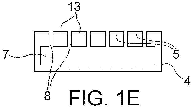
Figure 1B ) thus has a layer ofhydrocarbon 3 that must be transferred onto a substrate 4 (Figure 1C ). The substrate 4 (Figure 1C ) is of semiconductor material, for example silicon, having asurface 5 previously treated with an acid, for example hydrofluoric acid, ammonium fluoride, or a mixture thereof. - In
Figure 1C , thesubstrate 4 is a body provided with achamber 7 for housing a liquid andopenings 8, which are arranged according to a first pattern and which extend between thesurface 5 and thechamber 7 for enabling exit of the liquid from thechamber 7. - The support 1 is then put in contact with the
first surface 5 of thesubstrate 4, as shown inFigure 1D , for partially transferring the layer ofhydrocarbon 3 onto thesurface 5 of thesubstrate 4. The transfer step may have a duration comprised between 2 seconds and 1 minute. - In this way, transfer of the layer of
hydrocarbon 3 occurs in a way confined exclusively in the points of contact between the support 1 and thesurface 5 of thesubstrate 4, without involving theopenings 8 or thechamber 7. The structure ofFigure 1E is thus obtained, where present on thesurface 5 of thesubstrate 4 is ananti-wetting layer 13 formed by the material of the layer ofhydrocarbon 3. - Next, as illustrated in
Figure 1F , theanti-wetting layer 13 is fixed, i.e., chemically associated, to thesurface 5 of thesubstrate 4, for example, by heating at 200°C for 2 hours. - The chemical reaction that takes place between the
substrate 4 and theanti-wetting layer 13 is given inFigures 2A-2C . - As illustrated in
Figures 2A-2C , initially, thesubstrate 4 has a passivation layer 6 (for example, SiO2) on thesurface 5. The treatment, for instance with hydrofluoric acid, as described above with reference toFigure 1C , has the purpose of removing the passivation layer 6 and forming asilicon layer 12 that exposes hydrogen atoms (seeFigure 2B ). The layer ofhydrocarbon 3 is then transferred onto thelayer 12. Subsequent heating causes thehydrocarbon 3 to be firmly fixed to thesubstrate 4 by stable Si-C chemical bonds, thus forming theanti-wetting layer 13. - In another embodiment, illustrated in
Figures 3A-3H , for transferring of the layer ofhydrocarbon 3 from the support 1 to thesurface 5 of the substrate 4 amould 9 is used (Figure 3C ). Themould 9, which is, for example, of PDMS or PTFE, has asurface 11 that presentscavities 10 arranged according to a second pattern identical to that of theopenings 8 on thesurface 5 of thesubstrate 4. Thecavities 10 are further congruent to theopenings 8 present on thesurface 5 of thesubstrate 4. - Here, initially, as illustrated in
Figures 3A-3B , the layer ofhydrocarbon 3 is deposited on the support 1, as has been described with reference toFigures 1A-1B . Then, as illustrated inFigure 3D , thesurface 11 of themould 9 is put in contact with the layer ofhydrocarbon 3 on the support 1, for example for a time ranging from 2 seconds to 1 minute, for transferring part of the layer ofhydrocarbon 3 onto thesurface 11 of theflexible mould 9, to form atransfer layer 23, of the same material as the layer of hydrocarbon 3 (Figure 3E ). - The
transfer layer 23 present on thesurface 11 of themould 9 is then put in contact with thesurface 5 of thesubstrate 4, for example for a time ranging from 2 seconds to 1 minute, in such a way that theopenings 8 are aligned with the cavities 10 (Figure 3F ). - In this way, the
transfer layer 23 is transferred onto thesurface 5 of thesubstrate 4 precisely and in a confined way, without any risk of part of the molecules ofhydrocarbon 3 penetrating into theopenings 8 or into thechamber 7. - The
mould 9 may further be used also for transferring the layer ofhydrocarbon 3 onto asupport 4 without theopenings 8. Alternatively, amould 9 without thecavities 10 may be used for transferring the layer ofhydrocarbon 3 both onto asupport 4 withoutopenings 8 and onto a support that presents such openings. - Likewise, with reference to the embodiment illustrated in
Figures 1A-1F , also the support 1 may be provided with cavities similar to thecavities 10 of themould 9 for application of thehydrocarbon 3 in discrete areas of thesubstrate 4, which may also be without theopenings 8. - An example of application of the present method is creation of a chemically stable anti-wetting layer confined on the nozzle plate of an ink-jet printhead, shown schematically in
Figure 4 . Here the printhead, designated as a whole by 50, comprises abody 51, for example of silicon or glass, housing achamber 52 similar to thechamber 7 ofFigures 1C and3F . Anozzle plate 55 extends over thebody 51 and has at least onenozzle 56, similar to theopenings 8 ofFigures 1C and3F . Alternatively, thenozzle plate 55 may comprise a plurality of nozzles 56 (not shown), each connected to adifferent chamber 52. Thechamber 52 is connected to anexternal reservoir 60 through aninlet channel 61 and with thenozzle 56 through anoutlet channel 62. Amembrane 65 extends on one side of thechamber 52 in order to push the liquid contained in thechamber 52 towards thenozzle 56. Valves (not shown) enable the desired movement of the liquid, here an ink. - The top surface of the
nozzle plate 55 has ananti-wetting layer 68, obtained with the "contact printing" method described with reference toFigures 1A-1F or3A-3H . - The
anti-wetting layer 68 is deposited in a confined way, as described previously, in such a way also to prevent covering of the contacts (of whichFigure 4 shows just one, designated by 66) for electrical connection between electronic components (not shown) integrated within thebody 61 with the outside world, viawire 67, as well as covering of all those parts in which the anti-wetting coating is not required. - The above method may further be used for deposition of an anti-wetting layer on an ink-jet printhead of any type commercially available.
- Further characteristics of the present method will emerge from the ensuing description of some examples provided merely by way of non-limiting illustration.
- The first step of the process consisted in fabrication of a PDMS support.
- In detail, a prepolymeric mixture was prepared constituted by a base SYLGARD (R) 184 SILICONE ELASTOMER KIT and a cross-linking agent (Dow Corning) in the weight ratio 10:1. A degassing in vacuum conditions of the mixture was then carried out for one hour. The mixture thus obtained was deposited on a silicon master measuring 3 cm by 3 cm. The master was previously coated with a layer of organosilanes for enabling subsequent detachment of the PDMS support. The mixture deposited on the master was then cross-linked at 90°C in an oven for one hour, and the PDMS support thus obtained was detached from the silicon master.
- The PDMS support thus obtained was immersed in a solution of 1-hexadecene for 12 hours under nitrogen flow.
- The PDMS support was then removed from the solution of 1-hexadecene and exposed to nitrogen flow for 30 seconds in order to eliminate the excess liquid.
- It was then put in contact with a silicon substrate for 30 seconds in nitrogen atmosphere in order to transfer a layer of alkene exclusively in the contact areas.
- The silicon substrate was previously prepared by immersing it in a 2% HF aqueous solution for 2 minutes, followed by rinsing in distilled water for 30 seconds, in order to create hydrogen terminations on the surface itself.
- After contact between the PDMS support and the silicon substrate, a heating at 200°C in nitrogen was carried out for 2 hours, during which there occurred formation of the Si-C bonds according to the hydrosilation reaction.
- The support was then separated from the substrate, which was then washed in an appropriate organic solvent, such as mesitylene and the like, to remove the alkene that had not reacted.
- A nozzle plate for ink-jet printing provided according to the methodology illustrated in Example 1 was tested as regards its anti-wetting capacity.
- Four identical plates (specimens 1-4) of dimensions 40x12 mm were each introduced into a vial containing a water-based ink and containing the cyan pigment having a pH comprised between 7 and 9.
- Each plate was immersed for two thirds of their surface in the ink. The vials were then closed to prevent evaporation of the ink and set at the temperature of 60°C for 7 days.
- Next, the plates were removed from the vials and cleaned with demineralized water and then with 2-propanol. The plates were then dried.
- The anti-wetting capacity of the plates thus obtained was evaluated by measuring the angle of contact of a drop of water deposited thereon. In particular, comparisons were made between the values of the angle of contact on the plate prior to application of the anti-wetting layer according to the method described (Angle of contact prior to hydrosilation), of the angle of contact on the plate after application of the anti-wetting layer according to the method described (Angle of contact after hydrosilation), and of the angle of contact on the plate after immersion in the ink. The results obtained appear in Table 1.
Table 1 Sample Angle of contact prior to hydrosilation Angle of contact after hydrosilation Angle of contact after immersion in the ink 1 18.0 ± 1.3 107.3 ± 0.6 94.4 ± 2.0 2 16.2 ± 1.0 99.6 ± 1.0 95.9 ± 1.8 3 20.2 ± 0.6 104.4 ± 1.2 98.2 ± 2.0 4 19.3 ± 1.2 100.9 ± 0.5 92.5 ± 3.5 - As may be noted, notwithstanding immersion in a particularly aggressive ink, the values of the angle of contact remain very high (90% of the values after hydrosilation), indicating the goodness of the chemical resistance of the coating obtained with the method according to the invention.
- A plate of Example 2 (Sample 1) was compared with plates that had a coating obtained by silanization according to the prior art.
- In particular, the following samples having silanic coatings were provided:
- Sample 5: plate coated with FOTS (trichloro(1H,1H,2H,2H-perfluoro octyl)silane);
- Sample 6: plate coated with silane Fluorolink S10 (Solvay)
- Sample 7: plate coated with PTMS (propyl trimethoxysilane)
- Also in this case, the anti-wetting capacity was evaluated by measuring the angle of contact of a drop of water deposited on the specimens. The results appear in Table 2.
Table 2 Sample 1 Sample 5Sample 6 Sample 7Prior to immersion in ink 107.3± 0.6 108.7± 4.0 127.3± 2.6 103.0± 1.0 After immersion in ink 94.4± 2.0 <10 12 10.0 - Also in this case, it should be noted how the anti-wetting layer obtained with the method described, albeit presenting an initial angle of contact comparable with that of the coatings according to the prior art, is much more stable after contact with the ink.
- Four samples obtained according to what is illustrated in Example 1 were compared with two plates, the 1-hexadecene coating of which was applied by immersion of the plate in the alkene and subsequent heating (
Samples 8 and 9). In particular, saidsamples - In a round-bottom flask with a capacity of approximately 100 mL, 3 mL of pure 1-hexadecene were set to degas for approximately 1 hour in nitrogen. A silicon substrate (3 cm x 1 cm) previously immersed in a 2% (v/v) (40%) HF aqueous solution was then introduced into the flask for 2 minutes and then rinsed in distilled water for 30 seconds in order to obtain a surface with hydrogen terminations.
- The flask was immersed in an oil bath and kept at the temperature of 200°C for 2 hours, once again under nitrogen flow. Next, the substrate was taken out of the solution, washed and sonicated three times in mesitylene, and finally washed with distilled water and then dried with nitrogen.
- The anti-wetting capacity was evaluated by measuring the angle of contact of a drop of water deposited on the samples. The results appear in Table 3.
Table 3 Sample Angle of contact Sample 1 102.1 ± 3.4 Sample 2107.1 ± 2.2 Sample 3104.8 ± 1.2 Sample 4109.9 ± 0.4 sample 8104.6 ± 3.8 Sample 9105.3 ± 2.1 - As may be noted, the angles of contact between the samples obtained with the present method and those where the coating is applied by immersion are comparable. However, the method described enables application of the coating in an extremely confined way unlike the immersion method.
Claims (16)
- A method for application of an anti-wetting coating (13) to a substrate (4) of semiconductor material comprising the steps of:a) applying to a support (1) a solution of a hydrocarbon (3) comprising at least one unsaturated bond and, optionally, at least one hetero-atom for obtaining a layer of hydrocarbon (3);b) treating at least one surface (5) of a substrate (4) of semiconductor material with an acid;c) transferring said layer of hydrocarbon (3) from said support (1) to said surface (5) of said substrate (4) of semiconductor material; andd) chemically coupling said layer of hydrocarbon (3) to said surface (5) of said substrate (4) of semiconductor material.
- A method according to claim 1, characterized in that said hydrocarbon (3) is chosen in the group constituted by alkenes and alkynes.
- A method according to claim 1 or claim 2, characterized in that said hydrocarbon (3) contains from 8 to 20 carbon atoms.
- A method according to any one of the preceding claims, characterized in that said hydrocarbon (3) is chosen in the group constituted by 1-alkenes and 1-alkynes.
- A method according to claim 1, characterized in that said step a) is obtained by immersion of said support (1) in said solution of a hydrocarbon (3).
- A method according to claim 1, characterized in that said support (1) is of a material having a Young's modulus comprised between 100 kPa to 5 GPa.
- A method according to claim 1, characterized in that said acid is chosen in the group constituted by hydrofluoric acid, ammonium fluoride, or a mixture thereof.
- A method according to claim 1, characterized in that said step c) is obtained by putting in contact said support (1) with said surface (5) of said substrate (4) of semiconductor material.
- A method according to claim 1, characterized in that said step c) is obtained by using a mould (9).
- A method according to claim 1, characterized in that said substrate (4) of semiconductor material is a silicon substrate.
- A method according to any one of the preceding claims, characterized in that said substrate (4) of semiconductor material has first openings (8) arranged according to a first pattern.
- A method according to claim 11, characterized in that said substrate (4) of semiconductor material is a nozzle plate for ink-jet printing.
- A method according to claim 1, characterized in that said substrate (4) of semiconductor material has first openings (8) arranged according to a first pattern, and said step c) is obtained by using a mould (9) having cavities (10) arranged according to a second pattern identical to said first pattern, and said step c) is carried out by aligning said openings (8) with said cavities (10).
- A method according to claim 1, characterized in that said step d) is carried out by heating to a temperature comprised between 100 and 200°C.
- A method according to claim 1, characterized in that said step d) is carried out by UV irradiation.
- An integrated ink-jet printhead, comprising a body (51) of semiconductor material housing an ink chamber (52), an inlet channel (61) and an outlet channel (62), and a nozzle plate (55) which extends over the body (51), wherein the nozzle plate (55) is constituted by a support of semiconductor material covered with an anti-wetting coating (68) provided according to any one of claims 1-15.
Applications Claiming Priority (1)
| Application Number | Priority Date | Filing Date | Title |
|---|---|---|---|
| ITTO20141089 | 2014-12-22 |
Publications (2)
| Publication Number | Publication Date |
|---|---|
| EP3037267A1 true EP3037267A1 (en) | 2016-06-29 |
| EP3037267B1 EP3037267B1 (en) | 2018-08-22 |
Family
ID=52444584
Family Applications (1)
| Application Number | Title | Priority Date | Filing Date |
|---|---|---|---|
| EP15200611.0A Active EP3037267B1 (en) | 2014-12-22 | 2015-12-16 | Method for the surface treatment of a semiconductor substrate |
Country Status (3)
| Country | Link |
|---|---|
| US (2) | US9321269B1 (en) |
| EP (1) | EP3037267B1 (en) |
| CN (3) | CN107856417B (en) |
Families Citing this family (6)
| Publication number | Priority date | Publication date | Assignee | Title |
|---|---|---|---|---|
| US9321269B1 (en) * | 2014-12-22 | 2016-04-26 | Stmicroelectronics S.R.L. | Method for the surface treatment of a semiconductor substrate |
| IT201700034134A1 (en) | 2017-03-28 | 2018-09-28 | St Microelectronics Srl | FLUID-RELEASE DEVICE WITH CROSSTALK REDUCTION ELEMENT, PRINT HEAD INCLUDING THE EJECTION DEVICE, PRINTER INCLUDING THE PRINT HEAD AND PROCESS OF MANUFACTURING THE EJECTION DEVICE |
| WO2021021136A1 (en) | 2019-07-30 | 2021-02-04 | Hewlett-Packard Development Company L.P. | Uniform print head surface coating |
| US11666918B2 (en) * | 2020-03-06 | 2023-06-06 | Funai Electric Co., Ltd. | Microfluidic chip, head, and dispensing device for dispensing fluids containing an acidic component |
| WO2021211094A1 (en) | 2020-04-14 | 2021-10-21 | Hewlett-Packard Development Company, L.P. | Fluid-ejection die with stamped nanoceramic layer |
| WO2022230161A1 (en) * | 2021-04-30 | 2022-11-03 | コニカミノルタ株式会社 | Inkjet head and inkjet recording method |
Citations (4)
| Publication number | Priority date | Publication date | Assignee | Title |
|---|---|---|---|---|
| EP0367438A1 (en) * | 1988-10-19 | 1990-05-09 | Xaar Limited | Method of forming adherent fluorosilane layer on a substrate and ink jet recording head containing such a layer |
| EP1057643A2 (en) * | 1999-06-04 | 2000-12-06 | Eastman Kodak Company | Non-wetting protective layer for ink jet print heads |
| US20110050785A1 (en) * | 2009-09-02 | 2011-03-03 | Canon Kabushiki Kaisha | Liquid ejection head |
| WO2012173803A1 (en) * | 2011-06-15 | 2012-12-20 | 3M Innovative Properties Company | Hydrophobic hydrocarbon coatings |
Family Cites Families (15)
| Publication number | Priority date | Publication date | Assignee | Title |
|---|---|---|---|---|
| KR20050030956A (en) * | 2002-07-26 | 2005-03-31 | 코닌클리케 필립스 일렉트로닉스 엔.브이. | Micro-contact printing method |
| JP4293035B2 (en) * | 2003-05-07 | 2009-07-08 | セイコーエプソン株式会社 | Liquid repellent film covering member, component of liquid ejection device, nozzle plate of liquid ejection head, liquid ejection head, and liquid ejection device |
| GB0323295D0 (en) * | 2003-10-04 | 2003-11-05 | Dow Corning | Deposition of thin films |
| US7156488B2 (en) * | 2004-05-05 | 2007-01-02 | Eastman Kodak Company | Ink repellent coating on charge device to improve printer runability and printhead life |
| WO2006067668A1 (en) * | 2004-12-20 | 2006-06-29 | Koninklijke Philips Electronics N.V. | Surface patterning and via manufacturing employing controlled precipitative growth |
| US20090272715A1 (en) * | 2004-12-23 | 2009-11-05 | Koninklijke Philips Electronics, N.V. | Nanofabrication based on sam growth |
| KR20070055129A (en) * | 2005-11-25 | 2007-05-30 | 삼성전자주식회사 | Forming a hydrophobic coating film on the nozzle plate surface of the inkjet printhead |
| KR20080004225A (en) * | 2006-07-05 | 2008-01-09 | 삼성전자주식회사 | Nozzle plate of inkjet head and manufacturing method thereof |
| US7954926B2 (en) * | 2008-01-23 | 2011-06-07 | Lexmark International, Inc. | Hydrophobic nozzle plate structures for micro-fluid ejection heads |
| JP2012507418A (en) * | 2008-10-30 | 2012-03-29 | 富士フイルム株式会社 | Non-wetting coating on fluid ejection device |
| US8136922B2 (en) * | 2009-09-01 | 2012-03-20 | Xerox Corporation | Self-assembly monolayer modified printhead |
| US8262200B2 (en) * | 2009-09-15 | 2012-09-11 | Fujifilm Corporation | Non-wetting coating on a fluid ejector |
| US8534797B2 (en) * | 2009-12-28 | 2013-09-17 | Xerox Corporation | Superoleophobic and superhydrophobic devices and method for preparing same |
| CN102237304A (en) * | 2011-07-05 | 2011-11-09 | 复旦大学 | Method for inhibiting porous low dielectric constant medium from absorbing water vapor |
| US9321269B1 (en) * | 2014-12-22 | 2016-04-26 | Stmicroelectronics S.R.L. | Method for the surface treatment of a semiconductor substrate |
-
2015
- 2015-08-26 US US14/836,131 patent/US9321269B1/en active Active
- 2015-12-16 EP EP15200611.0A patent/EP3037267B1/en active Active
- 2015-12-22 CN CN201711060008.7A patent/CN107856417B/en active Active
- 2015-12-22 CN CN201521081379.XU patent/CN205364838U/en not_active Withdrawn - After Issue
- 2015-12-22 CN CN201510974309.5A patent/CN105711258B/en active Active
-
2016
- 2016-03-22 US US15/077,671 patent/US9724921B2/en active Active
Patent Citations (4)
| Publication number | Priority date | Publication date | Assignee | Title |
|---|---|---|---|---|
| EP0367438A1 (en) * | 1988-10-19 | 1990-05-09 | Xaar Limited | Method of forming adherent fluorosilane layer on a substrate and ink jet recording head containing such a layer |
| EP1057643A2 (en) * | 1999-06-04 | 2000-12-06 | Eastman Kodak Company | Non-wetting protective layer for ink jet print heads |
| US20110050785A1 (en) * | 2009-09-02 | 2011-03-03 | Canon Kabushiki Kaisha | Liquid ejection head |
| WO2012173803A1 (en) * | 2011-06-15 | 2012-12-20 | 3M Innovative Properties Company | Hydrophobic hydrocarbon coatings |
Also Published As
| Publication number | Publication date |
|---|---|
| CN105711258B (en) | 2017-12-08 |
| CN205364838U (en) | 2016-07-06 |
| CN107856417B (en) | 2019-12-24 |
| US9321269B1 (en) | 2016-04-26 |
| EP3037267B1 (en) | 2018-08-22 |
| US20160203973A1 (en) | 2016-07-14 |
| US9724921B2 (en) | 2017-08-08 |
| CN107856417A (en) | 2018-03-30 |
| CN105711258A (en) | 2016-06-29 |
Similar Documents
| Publication | Publication Date | Title |
|---|---|---|
| EP3037267B1 (en) | Method for the surface treatment of a semiconductor substrate | |
| US6020026A (en) | Process for the production of a coating of molecular thickness on a substrate | |
| CN102202900B (en) | Non-wetting coating on a fluid ejector | |
| CN101622579B (en) | Processed substrates having water-repellent areas in patterns, process for production thereof, and process for production of members having patterms made of functional material films | |
| WO2007102487A1 (en) | Treated substratum with hydrophilic region and water-repellent region and process for producing the same | |
| KR940005773A (en) | Method for producing chemisorbent membrane | |
| WO2009122660A1 (en) | Method of selectively arranging two types of materials on a substrate | |
| KR920014909A (en) | Water and oil repellent coating and its manufacturing method | |
| US20030235930A1 (en) | Multi-impression nanofeature production | |
| EP2295250A1 (en) | Self-assembly monolayer modified printhead | |
| KR100636263B1 (en) | Process for producing chemical adsorption film and chemical adsorption film | |
| CN104937694A (en) | Surface pretreatment and drop spreading control on multi component surfaces | |
| JP5768233B2 (en) | Method for controlling wettability of solid surface and solid surface thereof | |
| KR20140099409A (en) | Pattern transferring method using modification by self assembled monolayer | |
| Titova et al. | Efficient method for fabrication of reusable printed organic electrochemical transistors for liquid sensors based on the complex of poly (3, 4-ethylenedioxythiophene) with poly (styrenesulfonic acid) | |
| KR100613000B1 (en) | Substrate for a display and method for manufacturing the same | |
| KR101535069B1 (en) | Method for forming hydrophilic or hydrophobic coating layer on surface of polycarbonate substrate and method for manufacturing polycarbonate substrate assembly having hydrophilic or hydrophobic microchannels | |
| EP2944471A1 (en) | Method for manufacturing water-repellent film, and substrate, nozzle plate, ink jet head, and ink jet recording device | |
| JP2008137306A (en) | Mold, its manufacturing method and molding produced with it | |
| KR20190042602A (en) | Modification method of solid surface | |
| Soliman et al. | Photochemical Preparation of Alkoxy Self-assembled Monolayers on Si from 1, 2-Epoxyalkane Molecules | |
| WO2009104235A1 (en) | Metal mold, process for manufacturing the same, and molded article produced using the mold | |
| JPH05116324A (en) | Ink jet discharge nozzle plate and its manufacture | |
| ITUB20159489A1 (en) | METHOD FOR THE SURFACE TREATMENT OF A SEMICONDUCTOR SUBSTRATE | |
| JPH04285566A (en) | Medical treatment material |
Legal Events
| Date | Code | Title | Description |
|---|---|---|---|
| PUAI | Public reference made under article 153(3) epc to a published international application that has entered the european phase |
Free format text: ORIGINAL CODE: 0009012 |
|
| AK | Designated contracting states |
Kind code of ref document: A1 Designated state(s): AL AT BE BG CH CY CZ DE DK EE ES FI FR GB GR HR HU IE IS IT LI LT LU LV MC MK MT NL NO PL PT RO RS SE SI SK SM TR |
|
| AX | Request for extension of the european patent |
Extension state: BA ME |
|
| 17P | Request for examination filed |
Effective date: 20161229 |
|
| RBV | Designated contracting states (corrected) |
Designated state(s): AL AT BE BG CH CY CZ DE DK EE ES FI FR GB GR HR HU IE IS IT LI LT LU LV MC MK MT NL NO PL PT RO RS SE SI SK SM TR |
|
| 17Q | First examination report despatched |
Effective date: 20170629 |
|
| GRAP | Despatch of communication of intention to grant a patent |
Free format text: ORIGINAL CODE: EPIDOSNIGR1 |
|
| INTG | Intention to grant announced |
Effective date: 20180307 |
|
| GRAS | Grant fee paid |
Free format text: ORIGINAL CODE: EPIDOSNIGR3 |
|
| GRAA | (expected) grant |
Free format text: ORIGINAL CODE: 0009210 |
|
| AK | Designated contracting states |
Kind code of ref document: B1 Designated state(s): AL AT BE BG CH CY CZ DE DK EE ES FI FR GB GR HR HU IE IS IT LI LT LU LV MC MK MT NL NO PL PT RO RS SE SI SK SM TR |
|
| REG | Reference to a national code |
Ref country code: GB Ref legal event code: FG4D |
|
| REG | Reference to a national code |
Ref country code: CH Ref legal event code: EP |
|
| REG | Reference to a national code |
Ref country code: AT Ref legal event code: REF Ref document number: 1031988 Country of ref document: AT Kind code of ref document: T Effective date: 20180915 |
|
| REG | Reference to a national code |
Ref country code: IE Ref legal event code: FG4D |
|
| REG | Reference to a national code |
Ref country code: DE Ref legal event code: R096 Ref document number: 602015015045 Country of ref document: DE |
|
| REG | Reference to a national code |
Ref country code: NL Ref legal event code: MP Effective date: 20180822 |
|
| REG | Reference to a national code |
Ref country code: LT Ref legal event code: MG4D |
|
| PG25 | Lapsed in a contracting state [announced via postgrant information from national office to epo] |
Ref country code: GR Free format text: LAPSE BECAUSE OF FAILURE TO SUBMIT A TRANSLATION OF THE DESCRIPTION OR TO PAY THE FEE WITHIN THE PRESCRIBED TIME-LIMIT Effective date: 20181123 Ref country code: NL Free format text: LAPSE BECAUSE OF FAILURE TO SUBMIT A TRANSLATION OF THE DESCRIPTION OR TO PAY THE FEE WITHIN THE PRESCRIBED TIME-LIMIT Effective date: 20180822 Ref country code: BG Free format text: LAPSE BECAUSE OF FAILURE TO SUBMIT A TRANSLATION OF THE DESCRIPTION OR TO PAY THE FEE WITHIN THE PRESCRIBED TIME-LIMIT Effective date: 20181122 Ref country code: RS Free format text: LAPSE BECAUSE OF FAILURE TO SUBMIT A TRANSLATION OF THE DESCRIPTION OR TO PAY THE FEE WITHIN THE PRESCRIBED TIME-LIMIT Effective date: 20180822 Ref country code: NO Free format text: LAPSE BECAUSE OF FAILURE TO SUBMIT A TRANSLATION OF THE DESCRIPTION OR TO PAY THE FEE WITHIN THE PRESCRIBED TIME-LIMIT Effective date: 20181122 Ref country code: IS Free format text: LAPSE BECAUSE OF FAILURE TO SUBMIT A TRANSLATION OF THE DESCRIPTION OR TO PAY THE FEE WITHIN THE PRESCRIBED TIME-LIMIT Effective date: 20181222 Ref country code: LT Free format text: LAPSE BECAUSE OF FAILURE TO SUBMIT A TRANSLATION OF THE DESCRIPTION OR TO PAY THE FEE WITHIN THE PRESCRIBED TIME-LIMIT Effective date: 20180822 Ref country code: FI Free format text: LAPSE BECAUSE OF FAILURE TO SUBMIT A TRANSLATION OF THE DESCRIPTION OR TO PAY THE FEE WITHIN THE PRESCRIBED TIME-LIMIT Effective date: 20180822 Ref country code: SE Free format text: LAPSE BECAUSE OF FAILURE TO SUBMIT A TRANSLATION OF THE DESCRIPTION OR TO PAY THE FEE WITHIN THE PRESCRIBED TIME-LIMIT Effective date: 20180822 |
|
| REG | Reference to a national code |
Ref country code: AT Ref legal event code: MK05 Ref document number: 1031988 Country of ref document: AT Kind code of ref document: T Effective date: 20180822 |
|
| PG25 | Lapsed in a contracting state [announced via postgrant information from national office to epo] |
Ref country code: AL Free format text: LAPSE BECAUSE OF FAILURE TO SUBMIT A TRANSLATION OF THE DESCRIPTION OR TO PAY THE FEE WITHIN THE PRESCRIBED TIME-LIMIT Effective date: 20180822 Ref country code: LV Free format text: LAPSE BECAUSE OF FAILURE TO SUBMIT A TRANSLATION OF THE DESCRIPTION OR TO PAY THE FEE WITHIN THE PRESCRIBED TIME-LIMIT Effective date: 20180822 Ref country code: HR Free format text: LAPSE BECAUSE OF FAILURE TO SUBMIT A TRANSLATION OF THE DESCRIPTION OR TO PAY THE FEE WITHIN THE PRESCRIBED TIME-LIMIT Effective date: 20180822 |
|
| PG25 | Lapsed in a contracting state [announced via postgrant information from national office to epo] |
Ref country code: PL Free format text: LAPSE BECAUSE OF FAILURE TO SUBMIT A TRANSLATION OF THE DESCRIPTION OR TO PAY THE FEE WITHIN THE PRESCRIBED TIME-LIMIT Effective date: 20180822 Ref country code: EE Free format text: LAPSE BECAUSE OF FAILURE TO SUBMIT A TRANSLATION OF THE DESCRIPTION OR TO PAY THE FEE WITHIN THE PRESCRIBED TIME-LIMIT Effective date: 20180822 Ref country code: CZ Free format text: LAPSE BECAUSE OF FAILURE TO SUBMIT A TRANSLATION OF THE DESCRIPTION OR TO PAY THE FEE WITHIN THE PRESCRIBED TIME-LIMIT Effective date: 20180822 Ref country code: ES Free format text: LAPSE BECAUSE OF FAILURE TO SUBMIT A TRANSLATION OF THE DESCRIPTION OR TO PAY THE FEE WITHIN THE PRESCRIBED TIME-LIMIT Effective date: 20180822 Ref country code: RO Free format text: LAPSE BECAUSE OF FAILURE TO SUBMIT A TRANSLATION OF THE DESCRIPTION OR TO PAY THE FEE WITHIN THE PRESCRIBED TIME-LIMIT Effective date: 20180822 Ref country code: IT Free format text: LAPSE BECAUSE OF FAILURE TO SUBMIT A TRANSLATION OF THE DESCRIPTION OR TO PAY THE FEE WITHIN THE PRESCRIBED TIME-LIMIT Effective date: 20180822 Ref country code: AT Free format text: LAPSE BECAUSE OF FAILURE TO SUBMIT A TRANSLATION OF THE DESCRIPTION OR TO PAY THE FEE WITHIN THE PRESCRIBED TIME-LIMIT Effective date: 20180822 |
|
| REG | Reference to a national code |
Ref country code: DE Ref legal event code: R097 Ref document number: 602015015045 Country of ref document: DE |
|
| PG25 | Lapsed in a contracting state [announced via postgrant information from national office to epo] |
Ref country code: SK Free format text: LAPSE BECAUSE OF FAILURE TO SUBMIT A TRANSLATION OF THE DESCRIPTION OR TO PAY THE FEE WITHIN THE PRESCRIBED TIME-LIMIT Effective date: 20180822 Ref country code: SM Free format text: LAPSE BECAUSE OF FAILURE TO SUBMIT A TRANSLATION OF THE DESCRIPTION OR TO PAY THE FEE WITHIN THE PRESCRIBED TIME-LIMIT Effective date: 20180822 Ref country code: DK Free format text: LAPSE BECAUSE OF FAILURE TO SUBMIT A TRANSLATION OF THE DESCRIPTION OR TO PAY THE FEE WITHIN THE PRESCRIBED TIME-LIMIT Effective date: 20180822 |
|
| PLBE | No opposition filed within time limit |
Free format text: ORIGINAL CODE: 0009261 |
|
| STAA | Information on the status of an ep patent application or granted ep patent |
Free format text: STATUS: NO OPPOSITION FILED WITHIN TIME LIMIT |
|
| 26N | No opposition filed |
Effective date: 20190523 |
|
| REG | Reference to a national code |
Ref country code: CH Ref legal event code: PL |
|
| PG25 | Lapsed in a contracting state [announced via postgrant information from national office to epo] |
Ref country code: SI Free format text: LAPSE BECAUSE OF FAILURE TO SUBMIT A TRANSLATION OF THE DESCRIPTION OR TO PAY THE FEE WITHIN THE PRESCRIBED TIME-LIMIT Effective date: 20180822 Ref country code: MC Free format text: LAPSE BECAUSE OF FAILURE TO SUBMIT A TRANSLATION OF THE DESCRIPTION OR TO PAY THE FEE WITHIN THE PRESCRIBED TIME-LIMIT Effective date: 20180822 Ref country code: LU Free format text: LAPSE BECAUSE OF NON-PAYMENT OF DUE FEES Effective date: 20181216 |
|
| REG | Reference to a national code |
Ref country code: IE Ref legal event code: MM4A |
|
| REG | Reference to a national code |
Ref country code: BE Ref legal event code: MM Effective date: 20181231 |
|
| PG25 | Lapsed in a contracting state [announced via postgrant information from national office to epo] |
Ref country code: IE Free format text: LAPSE BECAUSE OF NON-PAYMENT OF DUE FEES Effective date: 20181216 Ref country code: FR Free format text: LAPSE BECAUSE OF NON-PAYMENT OF DUE FEES Effective date: 20181231 |
|
| PG25 | Lapsed in a contracting state [announced via postgrant information from national office to epo] |
Ref country code: BE Free format text: LAPSE BECAUSE OF NON-PAYMENT OF DUE FEES Effective date: 20181231 |
|
| PG25 | Lapsed in a contracting state [announced via postgrant information from national office to epo] |
Ref country code: CH Free format text: LAPSE BECAUSE OF NON-PAYMENT OF DUE FEES Effective date: 20181231 Ref country code: LI Free format text: LAPSE BECAUSE OF NON-PAYMENT OF DUE FEES Effective date: 20181231 |
|
| PG25 | Lapsed in a contracting state [announced via postgrant information from national office to epo] |
Ref country code: MT Free format text: LAPSE BECAUSE OF NON-PAYMENT OF DUE FEES Effective date: 20181216 |
|
| PG25 | Lapsed in a contracting state [announced via postgrant information from national office to epo] |
Ref country code: TR Free format text: LAPSE BECAUSE OF FAILURE TO SUBMIT A TRANSLATION OF THE DESCRIPTION OR TO PAY THE FEE WITHIN THE PRESCRIBED TIME-LIMIT Effective date: 20180822 |
|
| PG25 | Lapsed in a contracting state [announced via postgrant information from national office to epo] |
Ref country code: PT Free format text: LAPSE BECAUSE OF FAILURE TO SUBMIT A TRANSLATION OF THE DESCRIPTION OR TO PAY THE FEE WITHIN THE PRESCRIBED TIME-LIMIT Effective date: 20180822 |
|
| PG25 | Lapsed in a contracting state [announced via postgrant information from national office to epo] |
Ref country code: CY Free format text: LAPSE BECAUSE OF FAILURE TO SUBMIT A TRANSLATION OF THE DESCRIPTION OR TO PAY THE FEE WITHIN THE PRESCRIBED TIME-LIMIT Effective date: 20180822 Ref country code: MK Free format text: LAPSE BECAUSE OF NON-PAYMENT OF DUE FEES Effective date: 20180822 Ref country code: HU Free format text: LAPSE BECAUSE OF FAILURE TO SUBMIT A TRANSLATION OF THE DESCRIPTION OR TO PAY THE FEE WITHIN THE PRESCRIBED TIME-LIMIT; INVALID AB INITIO Effective date: 20151216 |
|
| GBPC | Gb: european patent ceased through non-payment of renewal fee |
Effective date: 20191216 |
|
| PG25 | Lapsed in a contracting state [announced via postgrant information from national office to epo] |
Ref country code: GB Free format text: LAPSE BECAUSE OF NON-PAYMENT OF DUE FEES Effective date: 20191216 |
|
| PGFP | Annual fee paid to national office [announced via postgrant information from national office to epo] |
Ref country code: DE Payment date: 20251126 Year of fee payment: 11 |