EP3035662A1 - Image processing apparatus - Google Patents
Image processing apparatus Download PDFInfo
- Publication number
- EP3035662A1 EP3035662A1 EP15003590.5A EP15003590A EP3035662A1 EP 3035662 A1 EP3035662 A1 EP 3035662A1 EP 15003590 A EP15003590 A EP 15003590A EP 3035662 A1 EP3035662 A1 EP 3035662A1
- Authority
- EP
- European Patent Office
- Prior art keywords
- data
- error
- processing
- quantization
- input
- Prior art date
- Legal status (The legal status is an assumption and is not a legal conclusion. Google has not performed a legal analysis and makes no representation as to the accuracy of the status listed.)
- Granted
Links
Images



Classifications
-
- H—ELECTRICITY
- H04—ELECTRIC COMMUNICATION TECHNIQUE
- H04N—PICTORIAL COMMUNICATION, e.g. TELEVISION
- H04N1/00—Scanning, transmission or reproduction of documents or the like, e.g. facsimile transmission; Details thereof
- H04N1/40—Picture signal circuits
- H04N1/405—Halftoning, i.e. converting the picture signal of a continuous-tone original into a corresponding signal showing only two levels
-
- H—ELECTRICITY
- H04—ELECTRIC COMMUNICATION TECHNIQUE
- H04N—PICTORIAL COMMUNICATION, e.g. TELEVISION
- H04N1/00—Scanning, transmission or reproduction of documents or the like, e.g. facsimile transmission; Details thereof
- H04N1/40—Picture signal circuits
- H04N1/405—Halftoning, i.e. converting the picture signal of a continuous-tone original into a corresponding signal showing only two levels
- H04N1/4051—Halftoning, i.e. converting the picture signal of a continuous-tone original into a corresponding signal showing only two levels producing a dispersed dots halftone pattern, the dots having substantially the same size
- H04N1/4052—Halftoning, i.e. converting the picture signal of a continuous-tone original into a corresponding signal showing only two levels producing a dispersed dots halftone pattern, the dots having substantially the same size by error diffusion, i.e. transferring the binarising error to neighbouring dot decisions
-
- B—PERFORMING OPERATIONS; TRANSPORTING
- B41—PRINTING; LINING MACHINES; TYPEWRITERS; STAMPS
- B41J—TYPEWRITERS; SELECTIVE PRINTING MECHANISMS, i.e. MECHANISMS PRINTING OTHERWISE THAN FROM A FORME; CORRECTION OF TYPOGRAPHICAL ERRORS
- B41J2/00—Typewriters or selective printing mechanisms characterised by the printing or marking process for which they are designed
- B41J2/005—Typewriters or selective printing mechanisms characterised by the printing or marking process for which they are designed characterised by bringing liquid or particles selectively into contact with a printing material
- B41J2/01—Ink jet
-
- G—PHYSICS
- G03—PHOTOGRAPHY; CINEMATOGRAPHY; ANALOGOUS TECHNIQUES USING WAVES OTHER THAN OPTICAL WAVES; ELECTROGRAPHY; HOLOGRAPHY
- G03G—ELECTROGRAPHY; ELECTROPHOTOGRAPHY; MAGNETOGRAPHY
- G03G15/00—Apparatus for electrographic processes using a charge pattern
- G03G15/50—Machine control of apparatus for electrographic processes using a charge pattern, e.g. regulating differents parts of the machine, multimode copiers, microprocessor control
-
- G—PHYSICS
- G06—COMPUTING OR CALCULATING; COUNTING
- G06K—GRAPHICAL DATA READING; PRESENTATION OF DATA; RECORD CARRIERS; HANDLING RECORD CARRIERS
- G06K15/00—Arrangements for producing a permanent visual presentation of the output data, e.g. computer output printers
- G06K15/02—Arrangements for producing a permanent visual presentation of the output data, e.g. computer output printers using printers
- G06K15/18—Conditioning data for presenting it to the physical printing elements
- G06K15/1867—Post-processing of the composed and rasterized print image
- G06K15/1872—Image enhancement
- G06K15/1876—Decreasing spatial resolution; Dithering
-
- H—ELECTRICITY
- H04—ELECTRIC COMMUNICATION TECHNIQUE
- H04N—PICTORIAL COMMUNICATION, e.g. TELEVISION
- H04N1/00—Scanning, transmission or reproduction of documents or the like, e.g. facsimile transmission; Details thereof
- H04N1/46—Colour picture communication systems
- H04N1/56—Processing of colour picture signals
- H04N1/60—Colour correction or control
- H04N1/6027—Correction or control of colour gradation or colour contrast
-
- H—ELECTRICITY
- H04—ELECTRIC COMMUNICATION TECHNIQUE
- H04N—PICTORIAL COMMUNICATION, e.g. TELEVISION
- H04N1/00—Scanning, transmission or reproduction of documents or the like, e.g. facsimile transmission; Details thereof
- H04N1/40—Picture signal circuits
- H04N1/40087—Multi-toning, i.e. converting a continuous-tone signal for reproduction with more than two discrete brightnesses or optical densities, e.g. dots of grey and black inks on white paper
Definitions
- the present invention provides an image processing apparatus capable of effectively reducing the circuit scale in a configuration of executing the dither processing and the error diffusion processing using a common circuit.
- the multiplier 1103 generates values C', D', E' and F' by multiplying the error values obtained in the sutracter 1101 by coefficients C, D, E, and F, respectively.
- the multiplication value C' is gone through the buffer 1106 which stores the data of one pixel sequentially in the same manner and is added to the multiplication value D' in an adder 1107. Then, this addition result via the buffer 1108 is added to the multiplication value E' by an adder 1109. Moreover, this addition result via the buffer 1110 is added to the multiplication value F' by an adder 1111.
- a value obtained by adding the multiplication value by coefficient D for the error value of the processing object pixel, the multiplication value by coefficient C for the error value of the previously processed pixel, the multiplication value by coefficient E for the error value of the pixel processed two times before, and the multiplication value by coefficient F for the error value of the pixel processed three times before is output as error data 2.
- This error data 2 becomes the error data diffused to a one line lower pixel via the data buffer unit 104 as will be described below.
- a coefficient to calculate a correction amount for the inter-color correction to be described later is set as coefficient B corresponding to the error of the processing object pixel.
- error data 1 can be output to be added to the value of a neighboring processing object pixel (another color pixel in the case of dither processing as shown in FIG. 3C ) for the inter-color correction.
- "1" is set as coefficient B to calculate the inter-color correction amount (inter-color correction data).
- coefficient A is set to zero, it is also possible to perform the inter-color correction on the color data of two pixels ahead by setting a coefficient to calculate the inter-color correction amount to coefficient A.
- error data 2 is stored in the memory 1001 for each of the processing object pixels. Specifically, error data 2 is stored in an area (e.g., area 1) used as the input block being processed which includes the processing object pixel, among three areas shown in FIG. 6 . The storing of error data 2 of this input block being processed is performed on an area after data output (output completed area) among the areas to be used.
- area 1 e.g., area 1
- the storing of error data 2 of this input block being processed is performed on an area after data output (output completed area) among the areas to be used.
- the input addition value table is written into the memory 105. Then, in the case of executing the dither processing for the input image data, an input addition value of the pixel corresponding to the input block in the input addition value table is transferred from the memory 105 to the memory 1001 for each of the input blocks. Then, the input addition value corresponding to the processing object pixel of the input block related to the processing is output to the selector 1002 as the addition data.
- a comparison result for each of the pixels between the addition result and one threshold value ("128" in the present embodiment) in the quantization processing section 102 becomes equivalent to that obtained by the dither processing using a predetermined dither pattern.
- FIG. 8 shows an example of the case of quantizing the input image data of 256 gradation levels into binary data.
- the threshold value set in the quantization processing section 102 is 128, and the value of the input addition value table is generated by the subtraction of the threshold value of the above predetermined dither pattern from 128.
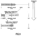
- FIG. 9 is a diagram explaining the inter-color correction processing in the case of the quantization into the binary data according to the present embodiment, and shows an example of performing the inter-color correction processing on the input image data of 256 gradation levels having three colors of A, B, and C.
- the inter-color correction amount is calculated by multiplying the inter-color correction coefficient B by the error calculated in the error calculation section 103.
- the quantization processing section 102 compares an addition result which is obtained in the input addition processing section 101 for color A by the addition of the pixel value of the input image data, error data 1 related to the processing of the previous color, and the input addition value, with the threshold value (128).
- the error thereof (255 - addition result) is added similarly as error data 1 (inter-color correction amount) in the input addition processing section 101 to provide the addition result of color B.
- this addition result is compared with the threshold value (128), and the error thereof becomes error data 1 (inter-color correction amount) for color C.
- the example shown in FIG. 9 is an example of assuming the inter-color correction coefficient B to be 1, and the errors in the quantization of color A and color B directly become the inter-color correction amounts for color B and color C.
- the value of the input addition value table is added included in error data 1. Therefore, the data buffer unit 104 selects value 0 as the addition data in the selector 1002 in the second or subsequent color processing.
- the inter-color correction processing makes it difficult to print a different color in a pixel where some color is already printed, and thereby it is possible to reduce the overlapping of inks as print color materials. Thereby, it is possible to reduce granular feeling of a print image.
- color A is printed in some pixel because exceeding the threshold value
- color B becomes difficult to be printed because color A is already printed.
- color C becomes easy to be printed because color B is not printed.
- the high speed memory 1001 within the data buffer unit 104 is divided into two areas as described above to be used as a double buffer ( FIG. 6 ).
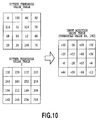
- the value (input addition value) for each of the pixels in the input addition value table set in this manner becomes a value obtained by the subtraction of the threshold values (64 and 192) set in the quantization processing section 102 from above threshold value of dither tables 1 and 2 assumed in the dither processing of the present embodiment, respectively.
- the present invention is not limited to this mode.
- the circuit configuring the quantization processing control section explained in the above described embodiment may be used in common for various printing apparatuses such as a printer, and the quantization by the error diffusion processing or the dither processing may be executed depending on a printing apparatus for use.
- the processing of the above explained quantization processing control section is assumed to be executed in the printing apparatus.
- the present invention is not limited to this mode, and the above described quantization processing may be executed by a host apparatus using the circuit configuration of the quantization processing control section, for example. Then, it is also possible to execute the processing by preparing a nonvolatile storage medium storing programs causing a computer to execute the processing and installing the programs.
- the present specification specifies an apparatus executing the above described quantization processing using the circuit configuration of the quantization processing control section to be an image processing apparatus including a printing apparatus such as a printer.
Landscapes
- Engineering & Computer Science (AREA)
- Multimedia (AREA)
- Signal Processing (AREA)
- Physics & Mathematics (AREA)
- General Physics & Mathematics (AREA)
- Microelectronics & Electronic Packaging (AREA)
- General Engineering & Computer Science (AREA)
- Theoretical Computer Science (AREA)
- Facsimile Image Signal Circuits (AREA)
- Image Processing (AREA)
- Color, Gradation (AREA)
Abstract
Description
- The present invention relates to an image processing apparatus, and specifically, relates to a technique of executing quantization processing by an error diffusion method and a dither method using a common circuit.
- Image data having a large number of gradation levels expressed by multiple values is converted into image data having a smaller number of gradation levels by quantization and thereby print data is generated in a printing apparatus such as an inkjet printing apparatus. Conventionally, in this quantization, processing by a dither method (hereinafter called "dither processing") and processing by an error diffusion method (hereinafter called "error diffusion processing") are executed using a common circuit (Japanese Patent Laid-Open No.
H06-233122 (1994 - In Japanese Patent Laid-Open No.
H06-233122 (1994 H06-233122 (1994 - The present invention provides an image processing apparatus capable of effectively reducing the circuit scale in a configuration of executing the dither processing and the error diffusion processing using a common circuit.
- The present invention in its one aspect provides an image processing apparatus comprising: a quantization unit (102) configured to generate quantized data having smaller gradation levels than that of the pre-quantization data by using a comparison threshold value with which pre-quantization data of a processing object pixel is compared; a generating unit (104) configured to include an error input section for inputting error data between the quantized data generated by the quantization unit and the pre-quantization data and a memory storing a value corresponding to a difference between the comparison threshold value and an original threshold value allocated in a threshold matrix that defines threshold values according to an arrangement of pixels and to generate the value corresponding to the difference as an addition data that is added to a value of an input image data of the processing object pixel, without using the error data input to the error input section for adjusting the input image data of the processing object pixel; and a processing unit (101) configured to add the value of the addition data generated by the generating unit to the value of the input image data of the processing object pixel to output input image data to which the value of the addition data is added.
- With the above configuration, it becomes possible to effectively reduce the circuit scale in a configuration of executing the dither processing and the error diffusion processing using a common circuit.
- Further features of the present invention will become apparent from the following description of exemplary embodiments (with reference to the attached drawings).
-
-
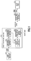
FIG. 1 is a block diagram showing a configuration for image processing in a printing apparatus according to an embodiment of the present invention; -
FIG. 2 is a block diagram showing a detailed configuration of a quantization processing control section shown inFIG. 1 ; -
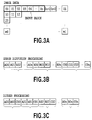
FIGS. 3A to 3C are diagrams explaining a processing section of image data in a quantizationprocessing control section 908 shown inFIG. 2 ; -
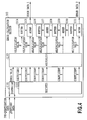
FIG. 4 is a block diagram showing a detailed circuit configuration of an error calculation section shown inFIG. 2 ; -
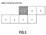
FIG. 5 is a diagram showing a pixel position to which error is diffused in error diffusion processing; -
FIG. 6 is a diagram showing divided areas of a high speed memory within a data buffer unit shown inFIG. 2 ; -
FIGS. 7A and 7B are block diagrams showing a detailed circuit configuration of adata buffer unit 104; -
FIG. 8 is a diagram explaining an input addition value table according to a first embodiment of the present invention; -
FIG. 9 is a diagram explaining inter-color correction processing in quantization into binary data according to the first embodiment; -
FIG. 10 is a diagram explaining an input addition value table according to a second embodiment of the present invention; and; and -
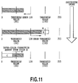
FIG. 11 is a diagram explaining inter-color correction processing in quantization into ternary data according to the second embodiment. - In the following, there will be explained embodiments of the present invention in detail with reference to the attached drawings.
-
FIG. 1 is a block diagram mainly showing a configuration for image processing in a printing apparatus according to an embodiment of the present invention, and the image processing configuration shown in the drawing is expressed as a processing function executed by a computer in the printing apparatus, except for circuits configuration to be explained in the following. - The printing apparatus of the present embodiment, as shown in
FIG. 1 , includes animage processing section 901, adata reception section 902, a printdata generation section 903, and aprint head 904. Thedata reception section 902 receives image data from a host apparatus such as a computer and a camera, and transmits the image data to theimage processing section 901 as image data of a pixel unit. - The
image processing section 901 includes aprecedent processing section 905, asubsequent processing section 906, an output γ-correction section 907, and a quantizationprocessing control section 908. Theprecedent processing section 905 performs conversion of a color indicated by the image data for each pixel on the input image data of 8 bits and 256 gradation levels. More specifically, theprecedent processing section 905 performs gamut mapping of converting a color of a color gamut in the case that an image is reproduced in a host apparatus into a color of a color gamut in the case that the color is reproduced in the printing apparatus of the present embodiment. Thesubsequent processing section 906 converts the gamut-mapped input image data of the same 8 bits and 256 gradation levels into a combination of colors of inks ejected by theprint head 904, the combination of colors being able to express a color indicated by the image data for each pixel. The output γ-correction section 907 performs γ-correction for each ink color according to a print head characteristic on the image data subjected to the subsequent processing. Then, the quantizationprocessing control section 908, as will be described in detail inFIG. 2 and the following drawings, controls the quantization circuit of the present embodiment, quantizes the image data of 8 bits and 256 gradation levels, and outputs one bit binary data for each ink color. The quantizationprocessing control section 908 of the present embodiment changes a quantization mode according to a print mode. More specifically, the quantizationprocessing control section 908 executes quantization by the error diffusion processing and quantization by the dither processing using a common circuit, and executes the processing by switching the quantization by the error diffusion processing and the quantization by the dither processing depending on the print mode. For example, the quantization by the dither processing is performed in a mode in which print speed is given priority to image quality, and the quantization by the error diffusion processing is performed in a mode in which the image quality is given priority. - The print
data generation section 903 generates print data (head drive data) for ejection in theprint head 904 from the quantized binary image data, and transfers the print data to theprint head 904. - Note that, while an inkjet printing apparatus has been explained as an example of the printing apparatus in the above explanation, the printing apparatus to which the quantization processing explained in the present embodiment can be applied is not limited to a printing apparatus of this type. For example, it will become apparent also from the following explanation that this quantization processing can be applied to a printing apparatus of an electro-photographic type, a heat transfer type, or the like.
-
FIG. 2 is a block diagram showing a detailed configuration of the quantizationprocessing control section 908 shown inFIG. 1 . The quantization processing control section of the present embodiment includes an inputaddition processing section 101, aquantization processing section 102, anerror calculation section 103, adata buffer unit 104, and amemory 105, and realizes the functions of these processing sections as circuit configurations. Then, the quantization processing control section of the present embodiment selects and executes the quantization by the error diffusion processing or the quantization by the dither processing. -
FIGS. 3A to 3C are diagrams explaining a processing unit of the image data in the quantizationprocessing control section 908 shown inFIG. 2 . The quantizationprocessing control section 908 divides the input image data into input blocks each including a predetermined number of pixels, and performs the processing for each of the input blocks.FIG. 3A shows an example of the input block in the input image data, and shows that the input block is configured with n+1 pixels (00 to On), (0n + 1 to 02(n + 1)), ··· in a width direction, in the case that the image data has an image width of 1 + 1 and an image height of m+1. In the image data, after the processing is finished for all the pixels of an input block, the processing is performed on the next input block neighboring in the width direction. Then, after the processing is finished for one pixel line in the width direction, the processing is performed similarly for each of the input blocks on one pixel line under the pixel line. - The processing for each of the pixels in the input block is performed in a different order between the case of the error diffusion processing and the case of the dither processing.
- In the case of executing the error diffusion processing, as shown in
FIG. 3B , the processing is performed for each color in the input block. Specifically, the processing order of the pixels in the input block is that the error diffusion processing is performed on apixel 00 in the image data of color A and then the processing is performed on the neighboringpixel 01 of the same color A. Then, after the error diffusion processing is finished for allpixels 00 to 0n in the block for color A, the processing is performed in the same manner onpixels 00 to 0n at the same pixel positions for next color B, and the processing is performed in the same manner also on next color C. - In the case of executing the dither processing, as shown in
FIG. 3C , the processing is performed for each of the pixels in the input block. Specifically, after the dither processing is performed on the pixel value of color A inpixel 00, the processing is performed sequentially on color B in thesame pixel 00 and on the color C in thesame pixel 00. Then, after the processing is finished for all colors A to C onpixel 00, the dither processing is performed onnext pixel 01. - With reference to
FIG. 2 again, the pixel data of 8 bits and 256 gradation levels is input as the input image data into the inputaddition processing section 101 in the quantizationprocessing control section 908, in a unit of one color for one pixel. The inputaddition processing section 101 adds addition data stored in thedata buffer unit 104 anderror data 1 of error data calculated by theerror calculation section 103, to this input image data. The data after the addition of these pieces of data is input into thequantization processing section 102 as pre-quantization data. The inputaddition processing section 101 of the present embodiment has a maximum value and a minimum value of the pre-quantization data, and clips the above data after the addition to the maximum value in the case that the data after the addition has a value not smaller than the maximum value of the pre-quantization data, and to the minimum value in the case that the data after the addition has a value not larger than the minimum value of the pre-quantization value. The addition data input from thedata buffer unit 104, as will be described later in detail, has a different content between the case of the error diffusion processing and the case of the dither processing. - The
quantization processing section 102 quantizes the pre-quantization data input from the inputaddition processing section 101, and outputs the result as quantized data which is the binary data in the present embodiment. Thequantization processing section 102 has one threshold value data to obtain the binary data, uses this threshold value in common between the case of performing the error diffusion processing and the case of performing the dither processing. That is, originally one threshold value is used in the quantization by the error diffusion processing, and this threshold value is used in common. On the other hand, in the case that the quantization by the dither processing is performed, the input addition value table to be described later is included in the addition data from thedata buffer unit 104. Thereby, a value of the input addition value table is added to this common threshold value for each of the pixels, and a pattern having a predetermined size and different threshold values, that is, a dither pattern (matrix) is configured. - Note that, while the present embodiment is an example of obtaining the binary quantized data, as will be described later also in a second embodiment, it is possible to use a mode of obtaining quantized data having three or more levels and the
quantization processing section 102 can have threshold values in a number corresponding to the number of these quantization levels. Then, it is possible to perform the quantization processing by using the respective threshold values in the error diffusion processing and the dither processing as described above. Further, as another mode of the quantization processing in thequantization processing section 102, it is possible to perform the quantization processing by multiplying the pre-quantization data by a quantization coefficient and carrying bit shift of the data after the multiplication. In this case, thequantization processing section 102 retains the quantization coefficients in a number corresponding to the number of quantization levels for the quantization, and the quantization coefficients are selected in a number corresponding to the number of quantization levels. - The
error calculation section 103 generates error data 1 (also called "first error data") and error data 2 (also called "second error data") by performing processing to be described in detail inFIG. 4 . In the case of the error diffusion processing, theerror calculation section 103 compares the quantized data and the pre-quantization data to calculate an error caused by the quantization. In detail, theerror calculation section 103 has a quantized data representative value according to the number of quantization levels (binary values (two levels) in the present embodiment) and the quantized data, and calculates the error by subtracting the quantized data representative value from the pre-quantization data. Further, theerror calculation section 103 retains the error of a processing object pixel and the error of a pixel processed in the past for the errors obtained by the subtraction as above, and coefficients to generate theerror data 1 and theerror data 2 based on these errors. Then, in the case of the error diffusion processing, as shown inFIG. 5 , theerror calculation section 103 outputs an error to be diffused to pixels in the same line as the line of the processing object pixel in the image data according to the above coefficient as theerror data 1, and outputs an error to be diffused to pixels in the line next to the line of the processing object pixel according to the above coefficient as theerror data 2. Theerror data 1 anderror data 2 thus output are input into the inputaddition processing section 101 and thedata buffer unit 104, respectively, and retained until the next line processing. - On the other hand, in the case of the dither processing, only coefficient B in
FIG. 4 is set to have a value except zero, and, as will be described later, theerror data 1 is output including the error of the previous pixel multiplied by coefficient B and the error data in this case is used for inter-color correction. -
FIG. 4 is a block diagram showing a detailed circuit configuration of theerror calculation section 103. InFIG. 4 , coefficients A to F are set in aregister 1102 depending on the error diffusion processing or the dither processing which is set corresponding to the print mode as described above inFIG. 1 . Asubtracter 1101 subtracts the pre-quantization data from the quantized data representative value corresponding to the input quantized data, and calculates the error of the processing object pixel. Specifically, in the case of the quantization into binary data as in the present embodiment, the quantized data representative value is "0" in the case that the quantized data is "0", and the quantized data representative value is "255" in the case that the quantized data is "1". The error value calculated in thesubtracter 1101 is provided for calculation using coefficients A to F in amultiplier 1103, anderror data 1 anderror data 2 are output finally. Further, each ofbuffers - In the case of executing the error diffusion processing, each of coefficients A to F is a ratio of diffusing (scattering) the error caused in the processing object pixel to another pixel.
FIG. 5 is a diagram showing a pixel position to which the error is diffused and the coefficient of the diffusion. As shown inFIG. 5 , in the same pixel line, the error is diffused to a pixel neighboring the processing object pixel on the right side at a ratio indicated by coefficient B, and the error is further diffused to a pixel neighboring the pixel to which the error is diffused, at a ratio indicated by coefficient A. Further, in the line which is one line lower than the line including the processing object pixel, the error is diffused to pixels at the lower right side, the directly lower side, and the lower left side of the processing object pixel at ratios indicated by coefficients C, D, and E, respectively, and the error is further diffused to a pixel neighboring the lower left side pixel on the left side at a ratio indicated by coefficient F. - The
multiplier 1103 generates values A' and B' by multiplying the error values obtained in thesubtracter 1101 by coefficients A and B, respectively. The multiplication value A' gone through thebuffer 1104 is added to the multiplication value B' by anadder 1105. As a result, a value obtained by adding the multiplication value by multiplying the error value of the processing object pixel by coefficient B and the multiplication value by multiplying the error value of the previously processed pixel by coefficient A is output aserror data 1. Thiserror data 1 is added to the input image data in the inputaddition processing section 101 as described above, and thereby the error is diffused to the next processing object pixel in the same pixel line as the line of the processing object pixel. Similarly, themultiplier 1103 generates values C', D', E' and F' by multiplying the error values obtained in thesutracter 1101 by coefficients C, D, E, and F, respectively. The multiplication value C' is gone through thebuffer 1106 which stores the data of one pixel sequentially in the same manner and is added to the multiplication value D' in anadder 1107. Then, this addition result via thebuffer 1108 is added to the multiplication value E' by anadder 1109. Moreover, this addition result via thebuffer 1110 is added to the multiplication value F' by anadder 1111. As a result, a value obtained by adding the multiplication value by coefficient D for the error value of the processing object pixel, the multiplication value by coefficient C for the error value of the previously processed pixel, the multiplication value by coefficient E for the error value of the pixel processed two times before, and the multiplication value by coefficient F for the error value of the pixel processed three times before is output aserror data 2. Thiserror data 2 becomes the error data diffused to a one line lower pixel via thedata buffer unit 104 as will be described below. - On the other hand, in the case of executing the dither processing, a coefficient to calculate a correction amount for the inter-color correction to be described later is set as coefficient B corresponding to the error of the processing object pixel. Thereby,
error data 1 can be output to be added to the value of a neighboring processing object pixel (another color pixel in the case of dither processing as shown inFIG. 3C ) for the inter-color correction. Note that, in the present embodiment, "1" is set as coefficient B to calculate the inter-color correction amount (inter-color correction data). Further, while coefficient A is set to zero, it is also possible to perform the inter-color correction on the color data of two pixels ahead by setting a coefficient to calculate the inter-color correction amount to coefficient A. Further, in the dither processing of the case without performing the inter-color correction processing, both of coefficient A and coefficient B are set to be zero. Moreover, in the dither processing, as will be described later, while coefficients C to F are set to be zero sinceerror data 2 is not used, instead of this embodiment, the values of coefficients C to F can be set to any values. - With reference to
FIG. 2 again, thedata buffer unit 104 switches betweenerror data 2 and the input addition value table for use in the error diffusion processing and the dither processing. More specifically, thedata buffer unit 104 outputs the addition data usingerror data 2 input from theerror calculation section 103 in the case of executing the error diffusion processing, and outputs the addition data using the input addition value table in the case of executing the dither processing. Thedata buffer unit 104 monitors the pixel position of the input image data in this output of the addition data, and inputs data corresponding to the pixel position of the input image data among the data retained in the memory to the inputaddition processing section 101 as the addition data. Thedata buffer unit 104 of the present embodiment retains the data using a temporary memory included therein and thememory 105 outside thedata buffer unit 104. The memory within thedata buffer unit 104 is a high speed memory having a small capacity but having a comparatively high access speed and will be described later inFIGS. 7A and 7B , while thememory 105 is a memory having a large capacity but having a comparatively low access speed. Retaining information which is necessary for the processing object pixel in the high speed memory makes it possible to realize high speed processing. The high speed memory within thedata buffer unit 104 is used by division into a plurality of areas according to the processing.FIG. 6 is a diagram showing divided areas of the high speed memory within thedata buffer unit 104. As shown inFIG. 6 , the high speed memory is used by division into three areas in the case of the error diffusion processing and used by division into two areas in the case of the dither processing. -
FIGS. 7A and 7B are block diagrams showing a detailed circuit configuration of thedata buffer unit 104, and show a data flow in the case of executing the error diffusion processing and a data flow in the case of executing the dither processing, respectively. InFIGS. 7A and 7B , thememory 1001 is the above high speed memory within the data buffer unit. Further, aselector 1002 selects whether the data stored in thememory 1001 is output orvalue 0 is output as the addition data output from thedata buffer unit 104. - In the case of executing the error diffusion processing, as shown in
FIG. 7A ,error data 2 is stored in thememory 1001 for each of the processing object pixels. Specifically,error data 2 is stored in an area (e.g., area 1) used as the input block being processed which includes the processing object pixel, among three areas shown inFIG. 6 . The storing oferror data 2 of this input block being processed is performed on an area after data output (output completed area) among the areas to be used. At the same time as this storing,error data 2 stored in an area (e.g., area 3) in thememory 1001 used for an input block before the input block including the processing object pixel, that is,error data 2 generated in the previous input block is transferred to thememory 105, and alsoerror data 2 to be used for the next input block is transferred from thememory 105 to an area (e.g. , area 2) in thememory 1001 to be used for the input block next to the input block including the processing object pixel. Specifically, thememory 105stores error data 2 generated on the previous input block during the processing of some input block and thereby sequentially accumulateserror data 2 for each of the pixels of one line. Then, for each of the input blocks, in processing of the input block before the processing timing for some input block, thememory 105outputs error data 2 related to the processing one line before, corresponding to each of the pixels, and storeserror data 2 into an area to be used for the input block. - The transfer between the
memory 105 and thememory 1001 is performed in a unit of the input block. The data stored in an area to be used for the input block being processed is output for each of the pixels from thememory 1001 to theselector 1002. Then, in the processing of the next block, an area to be used for the next input block (e.g., area 2) is converted to an area used for the input block being processed, an area used for the previous input block (e.g., area 3) is converted to an area to be used for the next input block, and an area (e.g., area 1) used for the input block being processed is converted to an area used for the previous input block, respectively. Note that, while the data transferred from thememory 1001 to the selector is output as the addition data, in the case that the input image data is the first line of a page, the error data from the previous line does not exist and thereforevalue 0 is selected to be output by theselector 1002. - With the above explained configuration of the quantization
processing control section 908,error data 1 is input into the inputaddition processing section 101 in the processing of the next pixel and added to the input pixel data.Error data 2 is stored in thedata buffer unit 104 and input into the inputaddition processing section 101 in the processing of the next line to be added to the input image data. Thereby, for example, the error to be added topixel 12 shown inFIG. 3A by the diffusion has a value obtained by the addition of [error of pixel 10] × coefficient A and [error of pixel 11] × coefficient B aserror data 1, and [error of pixel 01] × coefficient C, [error of pixel 02] × coefficient D + [error of pixel 03] × coefficient E, and [error of pixel 04] × coefficient F aserror data 2. Note that, for a pixel on which the error diffusion is not desired to be performed, setting zero to the coefficient of the corresponding pixel makes it possible not to perform the error diffusion. Further, the error retained within theerror calculation section 103 in the processing of the last pixel in the processing for each of the colors in the input block is retained for use in the processing of the first pixel in the next input block. Note that, in the case of processing the first pixel of a line, the error retained in theerror calculation section 103 is reset. - With reference to
FIG. 7B , in the case of executing the dither processing, before the processing of the input image data of one page, the input addition value table is written into thememory 105. Then, in the case of executing the dither processing for the input image data, an input addition value of the pixel corresponding to the input block in the input addition value table is transferred from thememory 105 to thememory 1001 for each of the input blocks. Then, the input addition value corresponding to the processing object pixel of the input block related to the processing is output to theselector 1002 as the addition data. By adding this addition data to the input image data in the input addition processing section 101 (FIG. 2 ), a comparison result for each of the pixels between the addition result and one threshold value ("128" in the present embodiment) in thequantization processing section 102 becomes equivalent to that obtained by the dither processing using a predetermined dither pattern. -
FIG. 8 is a diagram explaining the input addition value table according to an embodiment of the present invention. As shown inFIG. 8 , the input addition value table defines an input addition value for each of the pixels for an image pattern with a predetermined size (in an example shown in the drawing, 4 pixels by 4 pixels, for simple illustration and explanation), and is applied to an input image of a size corresponding this pattern (1 pixels × 4 pixels). The value (input addition value) for each of the pixels in the input addition value table is a difference value obtained by the subtraction of a threshold value of a predetermined dither table (dither pattern) assumed in the dither processing of the present embodiment from one threshold value (128) set for thequantization processing section 102. By adding this input addition value corresponding to each of the pixels to the input pixel data for each of the pixels, it is possible to obtain the same effect as that of a method in which the threshold value is varied according to the above predetermined dither pattern while keeping constant a threshold value in quantization in thequantization processing section 102.FIG. 8 shows an example of the case of quantizing the input image data of 256 gradation levels into binary data. The threshold value set in thequantization processing section 102 is 128, and the value of the input addition value table is generated by the subtraction of the threshold value of the above predetermined dither pattern from 128. - In the present embodiment, in the case of executing the dither processing, as described above, an
error calculation section 103 generates a correction amount for the inter-color correction from the pre-quantization data and the error thereof from the quantized data obtained by thequantization processing section 102 and outputs the correction amount aserror data 1. Then,error data 1 is added to the pixel value of the next color in the input image data by the inputaddition processing section 101. Note that, in the case that all the colors subjected to the inter-color correction have been processed for the pixel being processed, or in an inter-color case in which the inter-color correction is not performed, the error data retained in theerror calculation section 103 is reset. -
FIG. 9 is a diagram explaining the inter-color correction processing in the case of the quantization into the binary data according to the present embodiment, and shows an example of performing the inter-color correction processing on the input image data of 256 gradation levels having three colors of A, B, and C. As explained above, the inter-color correction amount is calculated by multiplying the inter-color correction coefficient B by the error calculated in theerror calculation section 103. As shown inFIG. 9 , thequantization processing section 102 compares an addition result which is obtained in the inputaddition processing section 101 for color A by the addition of the pixel value of the input image data,error data 1 related to the processing of the previous color, and the input addition value, with the threshold value (128). Then, the error thereof (255 - addition result) is added similarly as error data 1 (inter-color correction amount) in the inputaddition processing section 101 to provide the addition result of color B. Then, this addition result is compared with the threshold value (128), and the error thereof becomes error data 1 (inter-color correction amount) for color C. The example shown inFIG. 9 is an example of assuming the inter-color correction coefficient B to be 1, and the errors in the quantization of color A and color B directly become the inter-color correction amounts for color B and color C. Note that, in this inter-color processing, the value of the input addition value table is added included inerror data 1. Therefore, thedata buffer unit 104 selectsvalue 0 as the addition data in theselector 1002 in the second or subsequent color processing. - The inter-color correction processing makes it difficult to print a different color in a pixel where some color is already printed, and thereby it is possible to reduce the overlapping of inks as print color materials. Thereby, it is possible to reduce granular feeling of a print image. In the example shown in
FIG. 9 , while color A is printed in some pixel because exceeding the threshold value, color B becomes difficult to be printed because color A is already printed. Then, color C becomes easy to be printed because color B is not printed. In the case of the dither processing, thehigh speed memory 1001 within thedata buffer unit 104 is divided into two areas as described above to be used as a double buffer (FIG. 6 ). For example,area 1 is assumed to be an area used for the input block being processed andarea 2 is assumed to be an area used for the next input block. Thereby, thedata buffer unit 104 can select and output the data corresponding to a processing position in the input addition value table fromarea 1. Further, thedata buffer unit 104 can write the data to be used for the next input block in the input addition vale table intoarea 2 of the high speed memory within thedata buffer unit 104 from the large capacity memory in thememory 105 during the processing of the input block. Then, in the processing of the next input block, thearea 2 is used as an area used for the input block being processed, andarea 1 is used as an area to be used for the next input block, and thereby it is possible to use the memory efficiently. - A second embodiment of the present invention relates to a mode of quantizing multi-value image data into multi-values of three or more values in the quantization by the dither processing.
FIG. 10 is a diagram explaining an input addition value table according to the second embodiment of the present invention, andFIG. 11 is a diagram explaining inter-color correction processing in the case of quantization into three-value data according to the second embodiment. - As shown in
FIG. 10 , the threshold values set in thequantization processing section 102 are two values of 64 and 192 corresponding to the quantization into three-value data. Then, two tables of dither threshold value table 1 and dither threshold value table 2 are prepared as assumed dither patterns. Here, the threshold value for each of the pixels in the dither threshold value table 2 is a value obtained by the addition of 128 corresponding to a difference between the above twothreshold values quantization processing section 102 from above threshold value of dither tables 1 and 2 assumed in the dither processing of the present embodiment, respectively. - As shown in
FIG. 11 , also in the inter-color correction processing according to the present embodiment, thequantization processing section 102 compares an addition result for color A obtained by the addition of the pixel value of the input image data,error data 1 related to the previous color processing, and the input addition value in the inputaddition processing section 101, with each of the two threshold values (64 and 192). Then, the error thereof is calculated as a difference between 128 of a difference between the two threshold values (64 and 192) and the addition result. This error is similarly added as error data 1 (inter-color correction amount) in the inputaddition processing section 101 to provide the addition result of color B. Then, this addition result is compared similarly with the two threshold values (64 and 192), and the error thereof becomes error data 1 (inter-color correction amount) of color C. - While the above described embodiment switches between the error diffusion processing and the dither processing depending on the print mode, the present invention is not limited to this mode. For example, the circuit configuring the quantization processing control section explained in the above described embodiment may be used in common for various printing apparatuses such as a printer, and the quantization by the error diffusion processing or the dither processing may be executed depending on a printing apparatus for use.
- Further, the processing of the above explained quantization processing control section is assumed to be executed in the printing apparatus. However, the present invention is not limited to this mode, and the above described quantization processing may be executed by a host apparatus using the circuit configuration of the quantization processing control section, for example. Then, it is also possible to execute the processing by preparing a nonvolatile storage medium storing programs causing a computer to execute the processing and installing the programs. In this manner, the present specification specifies an apparatus executing the above described quantization processing using the circuit configuration of the quantization processing control section to be an image processing apparatus including a printing apparatus such as a printer.
- As explained above, according to the embodiments of the present invention, it is possible to perform the quantization by the error diffusion processing and the quantization by the dither processing using a common circuit including the processing except the common functions between these processing modes, and thereby it becomes possible to reduce the circuit scale of the quantization processing section by the common circuit.
- While the present invention has been described with reference to exemplary embodiments, it is to be understood that the invention is not limited to the disclosed exemplary embodiments. The scope of the following claims is to be accorded the broadest interpretation so as to encompass all such modifications and equivalent structures and functions.
Claims (15)
- An image processing apparatus comprising:a quantization unit (102) configured to generate quantized data having smaller gradation levels than that of the pre-quantization data by using a comparison threshold value with which pre-quantization data of a processing object pixel is compared;a generating unit (104) configured to include an error input section for inputting error data between the quantized data generated by the quantization unit and the pre-quantization data and a memory storing a value corresponding to a difference between the comparison threshold value and an original threshold value allocated in a threshold matrix that defines threshold values according to an arrangement of pixels and to generate the value corresponding to the difference as an addition data that is added to a value of an input image data of the processing object pixel, without using the error data input to the error input section for adjusting the input image data of the processing object pixel; anda processing unit (101) configured to add the value of the addition data generated by the generating unit to the value of the input image data of the processing object pixel to output input image data to which the value of the addition data is added.
- The image processing apparatus according to claim 1, wherein the memory which the generating unit includes stores a matrix that allocates the value corresponding to the difference for each of pixels in an image.
- The image processing apparatus according to claim 1 or 2, further comprising an error calculation unit (103) configured to calculate the error between the quantized data and the pre-quantization data based on the quantized data generated by the quantization unit and the pre-quantization data,
wherein the error calculation unit outputs the error data for the generating unit in which a calculated error is cancelled and the error data is input to the error input section of the generating unit. - The image processing apparatus according to any of claims 1 to 3, wherein the image data of the processing object pixel is reproduced with a plurality of color material of different colors on a print medium, the processing unit includes an error input section for inputting an error between the quantized data generated by the quantization unit and the pre-quantization data, performs processing for a first color of the color material for reproducing the image data of the processing obj ect pixel and then performs processing for a second color of the color material for reproducing the image data of the processing object pixel, and adds an error generated by the processing unit performing the processing for the first color of the image data of the processing object pixel, the error being input to the error input section, to the second color of the image data of the processing object pixel.
- The image processing apparatus according to claim 4, further comprising an error calculation unit configured to calculate the error between the quantized data and the pre-quantization data based on the quantized data generated by the quantization unit and the pre-quantization data,
wherein the error calculation unit outputs the calculated error data as a first error data for the processing unit and the processing unit uses the first error data input to the error input section of the processing unit to perform processing for the input image data. - The image processing apparatus according to claim 5, wherein the error calculation unitoutputs the first error data for the processing unit in which the error calculated for the first color is not cancelled in the case that the error for the first color generated in the processing for the first color performed by the quantization unit is used for the processing for the second color performed by the quantization unit, andoutputs the second error data for the processing unit in which the error calculated for the first color is cancelled in the case that the error for the first color generated in the processing for the first color performed by the quantization unit is not used for the processing for the second color performed by the quantization unit.
- The image processing apparatus according to claim 5, wherein the error calculation unit outputs second error data in which error calculated by the error calculation unit is cancelled and the second error data is input to the error input section of the processing unit.
- The image processing apparatus according to claim 3, wherein the image processing apparatus is capable of performing a first image processing mode in which error diffusion processing is performed and a second image processing mode in which dither processing is performed,in the first image processing mode, the error calculation unit outputs error data for the generating unit in which a calculated error is not cancelled, the error data is input to the error input section of the generating unit, the generating unit uses an error for a first color of a precedently processed first pixel, which is input to the error input section of the generating unit, in adjusting the value of data of the first color of a subsequently processed second pixel to the first pixel, andin the second image processing, the error calculation unit outputs error data for the generating unit in which a calculated error is cancelled.
- The image processing apparatus according to claim 8, wherein the first image processing mode is a print image quality priority mode and the second processing mode is a print speed priority mode.
- The image processing apparatus according to claim 8, wherein the generating unit uses a high-speed memory having a first access speed and a first capacity and a large capacity memory having a second access speed slower than the first speed and a second capacity greater than the first capacity, the high-speed memory being divided into three areas in a case of the first image processing mode and being divided into two areas in a case of the second image processing mode, and the generating unit gains an access between each of the areas of the high-speed memory and the large capacity memory.
- The image processing apparatus according to any of claims 1 to 10, wherein the input image data is processed in a processing unit of an input block consisting of a predetermined number of pixels, and the quantization unit performs the processing for each color in the input block in a case of the first image processing mode and performs the processing for each pixel in the input block in a case of the second image processing mode.
- The image processing apparatus according to any of claims 1 to 11, wherein the quantization unit generates the quantized data having three or more gradation levels smaller than that of the pre-quantization data, based on the pre-quantization data.
- The image processing apparatus according to any of claims 1 to 12, further comprising a printing unit configured to perform printing by applying color materials to a print medium based on a quantized result by the quantization unit.
- The image processing apparatus according to claim 13, wherein the printing unit includes an ink jet print head for ejecting ink.
- The image processing apparatus according to claim 13, wherein the printing unit performs printing in an electro-photographic method.
Applications Claiming Priority (1)
| Application Number | Priority Date | Filing Date | Title |
|---|---|---|---|
| JP2014254032A JP6448345B2 (en) | 2014-12-16 | 2014-12-16 | Image processing device |
Publications (2)
| Publication Number | Publication Date |
|---|---|
| EP3035662A1 true EP3035662A1 (en) | 2016-06-22 |
| EP3035662B1 EP3035662B1 (en) | 2019-08-28 |
Family
ID=54780039
Family Applications (1)
| Application Number | Title | Priority Date | Filing Date |
|---|---|---|---|
| EP15003590.5A Not-in-force EP3035662B1 (en) | 2014-12-16 | 2015-12-16 | Image processing apparatus |
Country Status (4)
| Country | Link |
|---|---|
| US (1) | US9456108B2 (en) |
| EP (1) | EP3035662B1 (en) |
| JP (1) | JP6448345B2 (en) |
| KR (1) | KR101911381B1 (en) |
Families Citing this family (3)
| Publication number | Priority date | Publication date | Assignee | Title |
|---|---|---|---|---|
| CN106034090B (en) * | 2015-03-20 | 2019-05-31 | 联想(北京)有限公司 | Information processing method and interchanger |
| US10269144B2 (en) * | 2017-08-14 | 2019-04-23 | Qualcomm Incorporated | Dither spatial noise aware redundancy bypass |
| JP7332367B2 (en) | 2019-07-10 | 2023-08-23 | キヤノン株式会社 | Image processing device and image processing method |
Citations (5)
| Publication number | Priority date | Publication date | Assignee | Title |
|---|---|---|---|---|
| JPH06233122A (en) | 1993-02-04 | 1994-08-19 | Ricoh Co Ltd | Image processing device |
| EP0859507A2 (en) * | 1996-12-18 | 1998-08-19 | Seiko Epson Corporation | Multilevel screening for color laser printer |
| JP2001136389A (en) * | 2000-09-21 | 2001-05-18 | Ricoh Co Ltd | Image processing device |
| JP2001218052A (en) * | 2000-01-31 | 2001-08-10 | Konica Corp | Circuit and method for pseudo gradation |
| US20120163713A1 (en) * | 2010-12-27 | 2012-06-28 | Ricoh Company, Ltd. | Error diffusion processing circuit |
Family Cites Families (9)
| Publication number | Priority date | Publication date | Assignee | Title |
|---|---|---|---|---|
| US5210602A (en) * | 1991-02-25 | 1993-05-11 | International Business Machines Corporation | Coupled-color error diffusion |
| US5515456A (en) * | 1993-10-26 | 1996-05-07 | Visual Edge Technology, Inc. | Process for providing digital halftone image with random error diffusion, color correction and enlargement |
| JP2002300398A (en) * | 2001-03-29 | 2002-10-11 | Ricoh Co Ltd | Image processing device |
| US7199905B2 (en) * | 2001-12-04 | 2007-04-03 | Xerox Corporation | Systems and methods for halftoning multiple color separation layers by interlayer error diffusion |
| JP3823933B2 (en) * | 2003-03-07 | 2006-09-20 | コニカミノルタビジネステクノロジーズ株式会社 | Image processing device |
| JP4241441B2 (en) * | 2004-03-03 | 2009-03-18 | コニカミノルタホールディングス株式会社 | Image processing apparatus, image processing method, and image processing program |
| US7369276B2 (en) * | 2004-03-05 | 2008-05-06 | Eastman Kodak Company | Multi-level halftoning providing improved texture uniformity |
| JP5369851B2 (en) * | 2008-09-16 | 2013-12-18 | 株式会社リコー | Image processing apparatus, image processing method, computer-executable program, and computer-readable recording medium |
| JP5605017B2 (en) * | 2010-06-28 | 2014-10-15 | 富士ゼロックス株式会社 | Image processing apparatus and image output apparatus using the same |
-
2014
- 2014-12-16 JP JP2014254032A patent/JP6448345B2/en not_active Expired - Fee Related
-
2015
- 2015-12-07 US US14/961,205 patent/US9456108B2/en not_active Expired - Fee Related
- 2015-12-09 KR KR1020150174884A patent/KR101911381B1/en not_active Expired - Fee Related
- 2015-12-16 EP EP15003590.5A patent/EP3035662B1/en not_active Not-in-force
Patent Citations (5)
| Publication number | Priority date | Publication date | Assignee | Title |
|---|---|---|---|---|
| JPH06233122A (en) | 1993-02-04 | 1994-08-19 | Ricoh Co Ltd | Image processing device |
| EP0859507A2 (en) * | 1996-12-18 | 1998-08-19 | Seiko Epson Corporation | Multilevel screening for color laser printer |
| JP2001218052A (en) * | 2000-01-31 | 2001-08-10 | Konica Corp | Circuit and method for pseudo gradation |
| JP2001136389A (en) * | 2000-09-21 | 2001-05-18 | Ricoh Co Ltd | Image processing device |
| US20120163713A1 (en) * | 2010-12-27 | 2012-06-28 | Ricoh Company, Ltd. | Error diffusion processing circuit |
Also Published As
| Publication number | Publication date |
|---|---|
| US9456108B2 (en) | 2016-09-27 |
| US20160173723A1 (en) | 2016-06-16 |
| KR101911381B1 (en) | 2018-10-24 |
| JP2016116108A (en) | 2016-06-23 |
| KR20160073311A (en) | 2016-06-24 |
| EP3035662B1 (en) | 2019-08-28 |
| JP6448345B2 (en) | 2019-01-09 |
Similar Documents
| Publication | Publication Date | Title |
|---|---|---|
| JP6587552B2 (en) | Image processing apparatus and image processing method | |
| JP6391555B2 (en) | Image processing apparatus, image processing method, and program | |
| US10033906B2 (en) | Image processing apparatus with improved quantization, image processing method and storage medium thereof | |
| US7190485B2 (en) | Method for multilevel printing of digital images using reduced colorant amounts | |
| US9406004B2 (en) | Image processing apparatus, image processing method, and storage medium | |
| US9456108B2 (en) | Image processing apparatus | |
| WO2016119858A1 (en) | Color printing look-up-table | |
| US8947735B2 (en) | Image processing apparatus and image processing method for performing error diffusion processing for each region of an image | |
| US9030714B2 (en) | Image processing apparatus and image processing method to set appropriate ink amount for character data and for image data | |
| US6671071B1 (en) | Threshold bias circuits for enhanced color error diffusion | |
| US8208751B2 (en) | Image processing apparatus, image processing method, and program | |
| US11657245B2 (en) | Image processing apparatus, image processing method, and storage medium | |
| US7327491B2 (en) | Image processing apparatus, image processing method, computer program and computer-readable storage medium | |
| KR20110007039A (en) | Image processing apparatus and image processing method | |
| JP5955109B2 (en) | Image processing method and image processing apparatus | |
| US6249354B1 (en) | Image processing apparatus and method | |
| JP6464826B2 (en) | Image processing device | |
| US11288558B2 (en) | Dithering based color conversion | |
| JP5068243B2 (en) | Image processing apparatus, image recording apparatus, and program | |
| JP6428383B2 (en) | Image processing device | |
| US10389910B2 (en) | Image processing apparatus, image processing method, and storage medium | |
| US20140055819A1 (en) | Image processing apparatus, method, and computer-readable medium | |
| JP6171398B2 (en) | printer | |
| JP5066509B2 (en) | Image processing apparatus, image recording apparatus, image processing method, image recording method, program, and storage medium | |
| JP2016019111A (en) | Image processing system, control method thereof, and program |
Legal Events
| Date | Code | Title | Description |
|---|---|---|---|
| PUAI | Public reference made under article 153(3) epc to a published international application that has entered the european phase |
Free format text: ORIGINAL CODE: 0009012 |
|
| AK | Designated contracting states |
Kind code of ref document: A1 Designated state(s): AL AT BE BG CH CY CZ DE DK EE ES FI FR GB GR HR HU IE IS IT LI LT LU LV MC MK MT NL NO PL PT RO RS SE SI SK SM TR |
|
| AX | Request for extension of the european patent |
Extension state: BA ME |
|
| STAA | Information on the status of an ep patent application or granted ep patent |
Free format text: STATUS: REQUEST FOR EXAMINATION WAS MADE |
|
| 17P | Request for examination filed |
Effective date: 20161222 |
|
| RBV | Designated contracting states (corrected) |
Designated state(s): AL AT BE BG CH CY CZ DE DK EE ES FI FR GB GR HR HU IE IS IT LI LT LU LV MC MK MT NL NO PL PT RO RS SE SI SK SM TR |
|
| STAA | Information on the status of an ep patent application or granted ep patent |
Free format text: STATUS: EXAMINATION IS IN PROGRESS |
|
| 17Q | First examination report despatched |
Effective date: 20170822 |
|
| GRAP | Despatch of communication of intention to grant a patent |
Free format text: ORIGINAL CODE: EPIDOSNIGR1 |
|
| STAA | Information on the status of an ep patent application or granted ep patent |
Free format text: STATUS: GRANT OF PATENT IS INTENDED |
|
| INTG | Intention to grant announced |
Effective date: 20190513 |
|
| GRAS | Grant fee paid |
Free format text: ORIGINAL CODE: EPIDOSNIGR3 |
|
| GRAA | (expected) grant |
Free format text: ORIGINAL CODE: 0009210 |
|
| STAA | Information on the status of an ep patent application or granted ep patent |
Free format text: STATUS: THE PATENT HAS BEEN GRANTED |
|
| RAP1 | Party data changed (applicant data changed or rights of an application transferred) |
Owner name: CANON KABUSHIKI KAISHA |
|
| AK | Designated contracting states |
Kind code of ref document: B1 Designated state(s): AL AT BE BG CH CY CZ DE DK EE ES FI FR GB GR HR HU IE IS IT LI LT LU LV MC MK MT NL NO PL PT RO RS SE SI SK SM TR |
|
| REG | Reference to a national code |
Ref country code: GB Ref legal event code: FG4D |
|
| REG | Reference to a national code |
Ref country code: CH Ref legal event code: EP |
|
| REG | Reference to a national code |
Ref country code: AT Ref legal event code: REF Ref document number: 1173875 Country of ref document: AT Kind code of ref document: T Effective date: 20190915 |
|
| REG | Reference to a national code |
Ref country code: IE Ref legal event code: FG4D |
|
| REG | Reference to a national code |
Ref country code: DE Ref legal event code: R096 Ref document number: 602015036543 Country of ref document: DE |
|
| REG | Reference to a national code |
Ref country code: NL Ref legal event code: MP Effective date: 20190828 |
|
| REG | Reference to a national code |
Ref country code: LT Ref legal event code: MG4D |
|
| PG25 | Lapsed in a contracting state [announced via postgrant information from national office to epo] |
Ref country code: BG Free format text: LAPSE BECAUSE OF FAILURE TO SUBMIT A TRANSLATION OF THE DESCRIPTION OR TO PAY THE FEE WITHIN THE PRESCRIBED TIME-LIMIT Effective date: 20191128 Ref country code: SE Free format text: LAPSE BECAUSE OF FAILURE TO SUBMIT A TRANSLATION OF THE DESCRIPTION OR TO PAY THE FEE WITHIN THE PRESCRIBED TIME-LIMIT Effective date: 20190828 Ref country code: NL Free format text: LAPSE BECAUSE OF FAILURE TO SUBMIT A TRANSLATION OF THE DESCRIPTION OR TO PAY THE FEE WITHIN THE PRESCRIBED TIME-LIMIT Effective date: 20190828 Ref country code: LT Free format text: LAPSE BECAUSE OF FAILURE TO SUBMIT A TRANSLATION OF THE DESCRIPTION OR TO PAY THE FEE WITHIN THE PRESCRIBED TIME-LIMIT Effective date: 20190828 Ref country code: HR Free format text: LAPSE BECAUSE OF FAILURE TO SUBMIT A TRANSLATION OF THE DESCRIPTION OR TO PAY THE FEE WITHIN THE PRESCRIBED TIME-LIMIT Effective date: 20190828 Ref country code: FI Free format text: LAPSE BECAUSE OF FAILURE TO SUBMIT A TRANSLATION OF THE DESCRIPTION OR TO PAY THE FEE WITHIN THE PRESCRIBED TIME-LIMIT Effective date: 20190828 Ref country code: NO Free format text: LAPSE BECAUSE OF FAILURE TO SUBMIT A TRANSLATION OF THE DESCRIPTION OR TO PAY THE FEE WITHIN THE PRESCRIBED TIME-LIMIT Effective date: 20191128 Ref country code: PT Free format text: LAPSE BECAUSE OF FAILURE TO SUBMIT A TRANSLATION OF THE DESCRIPTION OR TO PAY THE FEE WITHIN THE PRESCRIBED TIME-LIMIT Effective date: 20191230 |
|
| PG25 | Lapsed in a contracting state [announced via postgrant information from national office to epo] |
Ref country code: AL Free format text: LAPSE BECAUSE OF FAILURE TO SUBMIT A TRANSLATION OF THE DESCRIPTION OR TO PAY THE FEE WITHIN THE PRESCRIBED TIME-LIMIT Effective date: 20190828 Ref country code: ES Free format text: LAPSE BECAUSE OF FAILURE TO SUBMIT A TRANSLATION OF THE DESCRIPTION OR TO PAY THE FEE WITHIN THE PRESCRIBED TIME-LIMIT Effective date: 20190828 Ref country code: GR Free format text: LAPSE BECAUSE OF FAILURE TO SUBMIT A TRANSLATION OF THE DESCRIPTION OR TO PAY THE FEE WITHIN THE PRESCRIBED TIME-LIMIT Effective date: 20191129 Ref country code: IS Free format text: LAPSE BECAUSE OF FAILURE TO SUBMIT A TRANSLATION OF THE DESCRIPTION OR TO PAY THE FEE WITHIN THE PRESCRIBED TIME-LIMIT Effective date: 20191228 Ref country code: RS Free format text: LAPSE BECAUSE OF FAILURE TO SUBMIT A TRANSLATION OF THE DESCRIPTION OR TO PAY THE FEE WITHIN THE PRESCRIBED TIME-LIMIT Effective date: 20190828 Ref country code: LV Free format text: LAPSE BECAUSE OF FAILURE TO SUBMIT A TRANSLATION OF THE DESCRIPTION OR TO PAY THE FEE WITHIN THE PRESCRIBED TIME-LIMIT Effective date: 20190828 |
|
| REG | Reference to a national code |
Ref country code: AT Ref legal event code: MK05 Ref document number: 1173875 Country of ref document: AT Kind code of ref document: T Effective date: 20190828 |
|
| PG25 | Lapsed in a contracting state [announced via postgrant information from national office to epo] |
Ref country code: TR Free format text: LAPSE BECAUSE OF FAILURE TO SUBMIT A TRANSLATION OF THE DESCRIPTION OR TO PAY THE FEE WITHIN THE PRESCRIBED TIME-LIMIT Effective date: 20190828 |
|
| PG25 | Lapsed in a contracting state [announced via postgrant information from national office to epo] |
Ref country code: RO Free format text: LAPSE BECAUSE OF FAILURE TO SUBMIT A TRANSLATION OF THE DESCRIPTION OR TO PAY THE FEE WITHIN THE PRESCRIBED TIME-LIMIT Effective date: 20190828 Ref country code: IT Free format text: LAPSE BECAUSE OF FAILURE TO SUBMIT A TRANSLATION OF THE DESCRIPTION OR TO PAY THE FEE WITHIN THE PRESCRIBED TIME-LIMIT Effective date: 20190828 Ref country code: AT Free format text: LAPSE BECAUSE OF FAILURE TO SUBMIT A TRANSLATION OF THE DESCRIPTION OR TO PAY THE FEE WITHIN THE PRESCRIBED TIME-LIMIT Effective date: 20190828 Ref country code: EE Free format text: LAPSE BECAUSE OF FAILURE TO SUBMIT A TRANSLATION OF THE DESCRIPTION OR TO PAY THE FEE WITHIN THE PRESCRIBED TIME-LIMIT Effective date: 20190828 Ref country code: PL Free format text: LAPSE BECAUSE OF FAILURE TO SUBMIT A TRANSLATION OF THE DESCRIPTION OR TO PAY THE FEE WITHIN THE PRESCRIBED TIME-LIMIT Effective date: 20190828 Ref country code: DK Free format text: LAPSE BECAUSE OF FAILURE TO SUBMIT A TRANSLATION OF THE DESCRIPTION OR TO PAY THE FEE WITHIN THE PRESCRIBED TIME-LIMIT Effective date: 20190828 |
|
| PG25 | Lapsed in a contracting state [announced via postgrant information from national office to epo] |
Ref country code: IS Free format text: LAPSE BECAUSE OF FAILURE TO SUBMIT A TRANSLATION OF THE DESCRIPTION OR TO PAY THE FEE WITHIN THE PRESCRIBED TIME-LIMIT Effective date: 20200224 Ref country code: SK Free format text: LAPSE BECAUSE OF FAILURE TO SUBMIT A TRANSLATION OF THE DESCRIPTION OR TO PAY THE FEE WITHIN THE PRESCRIBED TIME-LIMIT Effective date: 20190828 Ref country code: SM Free format text: LAPSE BECAUSE OF FAILURE TO SUBMIT A TRANSLATION OF THE DESCRIPTION OR TO PAY THE FEE WITHIN THE PRESCRIBED TIME-LIMIT Effective date: 20190828 Ref country code: CZ Free format text: LAPSE BECAUSE OF FAILURE TO SUBMIT A TRANSLATION OF THE DESCRIPTION OR TO PAY THE FEE WITHIN THE PRESCRIBED TIME-LIMIT Effective date: 20190828 |
|
| REG | Reference to a national code |
Ref country code: DE Ref legal event code: R097 Ref document number: 602015036543 Country of ref document: DE |
|
| PLBE | No opposition filed within time limit |
Free format text: ORIGINAL CODE: 0009261 |
|
| STAA | Information on the status of an ep patent application or granted ep patent |
Free format text: STATUS: NO OPPOSITION FILED WITHIN TIME LIMIT |
|
| PG2D | Information on lapse in contracting state deleted |
Ref country code: IS |
|
| REG | Reference to a national code |
Ref country code: CH Ref legal event code: PL |
|
| 26N | No opposition filed |
Effective date: 20200603 |
|
| REG | Reference to a national code |
Ref country code: BE Ref legal event code: MM Effective date: 20191231 |
|
| PG25 | Lapsed in a contracting state [announced via postgrant information from national office to epo] |
Ref country code: MC Free format text: LAPSE BECAUSE OF FAILURE TO SUBMIT A TRANSLATION OF THE DESCRIPTION OR TO PAY THE FEE WITHIN THE PRESCRIBED TIME-LIMIT Effective date: 20190828 Ref country code: SI Free format text: LAPSE BECAUSE OF FAILURE TO SUBMIT A TRANSLATION OF THE DESCRIPTION OR TO PAY THE FEE WITHIN THE PRESCRIBED TIME-LIMIT Effective date: 20190828 |
|
| GBPC | Gb: european patent ceased through non-payment of renewal fee |
Effective date: 20191216 |
|
| PG25 | Lapsed in a contracting state [announced via postgrant information from national office to epo] |
Ref country code: GB Free format text: LAPSE BECAUSE OF NON-PAYMENT OF DUE FEES Effective date: 20191216 Ref country code: IE Free format text: LAPSE BECAUSE OF NON-PAYMENT OF DUE FEES Effective date: 20191216 Ref country code: LU Free format text: LAPSE BECAUSE OF NON-PAYMENT OF DUE FEES Effective date: 20191216 Ref country code: FR Free format text: LAPSE BECAUSE OF NON-PAYMENT OF DUE FEES Effective date: 20191231 |
|
| PG25 | Lapsed in a contracting state [announced via postgrant information from national office to epo] |
Ref country code: LI Free format text: LAPSE BECAUSE OF NON-PAYMENT OF DUE FEES Effective date: 20191231 Ref country code: BE Free format text: LAPSE BECAUSE OF NON-PAYMENT OF DUE FEES Effective date: 20191231 Ref country code: CH Free format text: LAPSE BECAUSE OF NON-PAYMENT OF DUE FEES Effective date: 20191231 |
|
| PG25 | Lapsed in a contracting state [announced via postgrant information from national office to epo] |
Ref country code: CY Free format text: LAPSE BECAUSE OF FAILURE TO SUBMIT A TRANSLATION OF THE DESCRIPTION OR TO PAY THE FEE WITHIN THE PRESCRIBED TIME-LIMIT Effective date: 20190828 |
|
| PG25 | Lapsed in a contracting state [announced via postgrant information from national office to epo] |
Ref country code: MT Free format text: LAPSE BECAUSE OF FAILURE TO SUBMIT A TRANSLATION OF THE DESCRIPTION OR TO PAY THE FEE WITHIN THE PRESCRIBED TIME-LIMIT Effective date: 20190828 Ref country code: HU Free format text: LAPSE BECAUSE OF FAILURE TO SUBMIT A TRANSLATION OF THE DESCRIPTION OR TO PAY THE FEE WITHIN THE PRESCRIBED TIME-LIMIT; INVALID AB INITIO Effective date: 20151216 |
|
| PG25 | Lapsed in a contracting state [announced via postgrant information from national office to epo] |
Ref country code: MK Free format text: LAPSE BECAUSE OF FAILURE TO SUBMIT A TRANSLATION OF THE DESCRIPTION OR TO PAY THE FEE WITHIN THE PRESCRIBED TIME-LIMIT Effective date: 20190828 |
|
| PGFP | Annual fee paid to national office [announced via postgrant information from national office to epo] |
Ref country code: DE Payment date: 20220616 Year of fee payment: 8 |
|
| REG | Reference to a national code |
Ref country code: DE Ref legal event code: R119 Ref document number: 602015036543 Country of ref document: DE |
|
| PG25 | Lapsed in a contracting state [announced via postgrant information from national office to epo] |
Ref country code: DE Free format text: LAPSE BECAUSE OF NON-PAYMENT OF DUE FEES Effective date: 20240702 |
|
| PG25 | Lapsed in a contracting state [announced via postgrant information from national office to epo] |
Ref country code: DE Free format text: LAPSE BECAUSE OF NON-PAYMENT OF DUE FEES Effective date: 20240702 |