EP3035553A1 - Enhancing data rate or range of near field communication using differential coil topology - Google Patents
Enhancing data rate or range of near field communication using differential coil topology Download PDFInfo
- Publication number
- EP3035553A1 EP3035553A1 EP15193983.2A EP15193983A EP3035553A1 EP 3035553 A1 EP3035553 A1 EP 3035553A1 EP 15193983 A EP15193983 A EP 15193983A EP 3035553 A1 EP3035553 A1 EP 3035553A1
- Authority
- EP
- European Patent Office
- Prior art keywords
- coil antenna
- recited
- signal
- data
- nfc
- Prior art date
- Legal status (The legal status is an assumption and is not a legal conclusion. Google has not performed a legal analysis and makes no representation as to the accuracy of the status listed.)
- Withdrawn
Links
Images


Classifications
-
- H—ELECTRICITY
- H04—ELECTRIC COMMUNICATION TECHNIQUE
- H04B—TRANSMISSION
- H04B5/00—Near-field transmission systems, e.g. inductive or capacitive transmission systems
- H04B5/20—Near-field transmission systems, e.g. inductive or capacitive transmission systems characterised by the transmission technique; characterised by the transmission medium
- H04B5/24—Inductive coupling
- H04B5/26—Inductive coupling using coils
-
- H—ELECTRICITY
- H01—ELECTRIC ELEMENTS
- H01Q—ANTENNAS, i.e. RADIO AERIALS
- H01Q7/00—Loop antennas with a substantially uniform current distribution around the loop and having a directional radiation pattern in a plane perpendicular to the plane of the loop
-
- H—ELECTRICITY
- H04—ELECTRIC COMMUNICATION TECHNIQUE
- H04B—TRANSMISSION
- H04B5/00—Near-field transmission systems, e.g. inductive or capacitive transmission systems
- H04B5/20—Near-field transmission systems, e.g. inductive or capacitive transmission systems characterised by the transmission technique; characterised by the transmission medium
- H04B5/24—Inductive coupling
- H04B5/26—Inductive coupling using coils
- H04B5/263—Multiple coils at either side
-
- H—ELECTRICITY
- H04—ELECTRIC COMMUNICATION TECHNIQUE
- H04B—TRANSMISSION
- H04B5/00—Near-field transmission systems, e.g. inductive or capacitive transmission systems
- H04B5/20—Near-field transmission systems, e.g. inductive or capacitive transmission systems characterised by the transmission technique; characterised by the transmission medium
- H04B5/24—Inductive coupling
- H04B5/26—Inductive coupling using coils
- H04B5/266—One coil at each side, e.g. with primary and secondary coils
-
- H—ELECTRICITY
- H04—ELECTRIC COMMUNICATION TECHNIQUE
- H04B—TRANSMISSION
- H04B5/00—Near-field transmission systems, e.g. inductive or capacitive transmission systems
- H04B5/70—Near-field transmission systems, e.g. inductive or capacitive transmission systems specially adapted for specific purposes
-
- H—ELECTRICITY
- H04—ELECTRIC COMMUNICATION TECHNIQUE
- H04B—TRANSMISSION
- H04B5/00—Near-field transmission systems, e.g. inductive or capacitive transmission systems
- H04B5/70—Near-field transmission systems, e.g. inductive or capacitive transmission systems specially adapted for specific purposes
- H04B5/77—Near-field transmission systems, e.g. inductive or capacitive transmission systems specially adapted for specific purposes for interrogation
-
- H—ELECTRICITY
- H04—ELECTRIC COMMUNICATION TECHNIQUE
- H04W—WIRELESS COMMUNICATION NETWORKS
- H04W4/00—Services specially adapted for wireless communication networks; Facilities therefor
- H04W4/80—Services using short range communication, e.g. near-field communication [NFC], radio-frequency identification [RFID] or low energy communication
-
- G—PHYSICS
- G06—COMPUTING OR CALCULATING; COUNTING
- G06Q—INFORMATION AND COMMUNICATION TECHNOLOGY [ICT] SPECIALLY ADAPTED FOR ADMINISTRATIVE, COMMERCIAL, FINANCIAL, MANAGERIAL OR SUPERVISORY PURPOSES; SYSTEMS OR METHODS SPECIALLY ADAPTED FOR ADMINISTRATIVE, COMMERCIAL, FINANCIAL, MANAGERIAL OR SUPERVISORY PURPOSES, NOT OTHERWISE PROVIDED FOR
- G06Q20/00—Payment architectures, schemes or protocols
- G06Q20/30—Payment architectures, schemes or protocols characterised by the use of specific devices or networks
- G06Q20/32—Payment architectures, schemes or protocols characterised by the use of specific devices or networks using wireless devices
- G06Q20/327—Short range or proximity payments by means of M-devices
- G06Q20/3278—RFID or NFC payments by means of M-devices
-
- H—ELECTRICITY
- H04—ELECTRIC COMMUNICATION TECHNIQUE
- H04B—TRANSMISSION
- H04B5/00—Near-field transmission systems, e.g. inductive or capacitive transmission systems
- H04B5/70—Near-field transmission systems, e.g. inductive or capacitive transmission systems specially adapted for specific purposes
- H04B5/79—Near-field transmission systems, e.g. inductive or capacitive transmission systems specially adapted for specific purposes for data transfer in combination with power transfer
Definitions
- a typical wireless communication and power transfer schemes in use today employ inductive coupling between a resonant first coil antenna and a resonant second coil antenna.
- the wireless communication includes near field communications (NFC) related functions or Europay, MasterCard and Visa (EMVCO) based contactless payment and wireless charging.
- NFC near field communications
- EMVCO Europay, MasterCard and Visa
- a mode of operation where a power for the operation of a passive tag is derived from a reader, in addition to the communication link.
- This mode of operation uses a strong carrier signal to power a tag and simultaneously tries to listen to a load modulated signal from the tag.
- ADC analog to digital converter
- Described herein are architectures, platforms and methods for increasing data rates and to enhance range during NFC related functions or transactions.
- a first coil antenna and a second coil antenna of a portable device are connected in series and are further disposed within the portable device to avoid presence of linkages between the two.
- the receiving of a modulated signal through the first coil antenna is not affected by a carrier signal or an operating frequency that is present at the second coil antenna, or vice versa.
- an NFC module may be configured to subtract the carrier signal at the second coil antenna from the received modulated data.
- the subtraction eliminates the carrier signal in the received modulated data and as such, a low-frequency modulating data is produced as a result.
- the low-frequency modulating data is fed to an analog to digital converter (ADC) to transform the modulating data from an analog to a digital signal.
- ADC analog to digital converter
- the ADC may not require a higher resolution feature as the carrier signal is already cancelled prior to the ADC processing.
- the dynamic range requirements at the receiver side of the portable device may be substantially reduced by using, for example, a lower resolution ADC
- FIG. 1 is an example scenario 100 that illustrates an NFC coupling arrangement as described in implementations herein.
- the NFC coupling arrangement demonstrates a particular implementation for obtaining higher data rates and an increase in range during NFC related functions or transactions between devices.
- Scenario 100 may include a portable device 102 with a first coil antenna 104-2 and a second coil antenna 104-4.
- the scenario 100 further shows a portable device 102 in near field coupling arrangement with a credit card 106 (e.g., payment transactions) or an NFC tag 108 (e.g., tag reading).
- a portable device 110 with an antenna 112 is shown to engage in near field coupling arrangement with the portable device 102 (e.g., NFC communications).
- the portable device 102 is utilized for payment transactions (e.g., EMVco transactions) for the credit card 106.
- the portable device 102 establishes near field coupling by aligning either the first coil antenna 104-2 or the second coil antenna 104-4 in the direction and within a certain distance of the credit card 106. At this certain distance, mutual induction between credit card strips (not shown) and the first or second coil antenna may facilitate data communications between the credit card 106 and the portable device 102.
- the NFC tag 108 and the portable device 110 may establish near field coupling arrangement with the portable device 102 in the same manner described above.
- coil strips (not shown) of the NFC tag 108 or the antenna 112 of the portable device 110 may be positioned at a certain distance to either the first or second coil antenna of the portable device 102 to engage in NFC communications.
- the first coil antenna 104-2 and the second coil antenna 104-2 of the portable device 102 may be connected in series and are disposed in a manner to avoid presence of flux linkages between the two.
- the first coil antenna 104-2 may be disposed on a display side and faces a user (not shown) while the second coil antenna 104-4 may be disposed at a corner or a back-side of the portable device 102.
- Other examples such as when the first and second coil antennas are at opposite corners of the portable device 102 may similarly apply as long as there is no flux linkages between the two.
- the NFC related functions or transactions may either be facilitated by the first coil antenna 104-2, or the second coil antenna 104-4.
- directing the credit card 106 to a coverage area of the first coil antenna 104-2 may facilitate the NFC related transaction between the two.
- the second coil antenna 104-4 which may be disposed at another end of the portable device 102, may not be a factor to this NFC related transaction.
- the NFC related transaction may be made between the credit card 106 and the second coil antenna 104-4.
- the first coil antenna 104-2 may be a non-factor during the process as described above.
- the NFC related transaction may utilize a modulated signal to transmit data.
- the first coil antenna 104-2 is configured to have an operating frequency of 13.56 MHz.
- the operating frequency of 13.56 MHz is a carrier signal that is modulated by data from the credit card 106 to produce the modulated signal at the first coil antenna 104-2.
- an NFC module may combine the received modulated signal from the first coil antenna 104-2 with a carrier signal (not shown) that is present in the second coil antenna 104-4, or vice-versa. That is, the NFC module may combine the received modulated signal from the second coil antenna 104-4 with the carrier signal from the first coil antenna 104-2.
- the carrier signal is cancelled to provide low-frequency data.
- the low-frequency data is fed to one receiving pin (not shown) of the NFC module before they are further converted to digital data by an analog to digital converter (ADC) (not shown).
- ADC analog to digital converter
- the ADC may not require higher resolution feature as the carrier signal is already cancelled prior to the ADC processing.
- the dynamic range requirements at the receiver side may be substantially reduced by using, for example, a lower resolution ADC.
- the portable devices 102 and 110 may include, but are not limited to, Ultrabooks, a tablet computer, a netbook, a notebook computer, a laptop computer, mobile phone, a cellular phone, a smartphone, a personal digital assistant, a multimedia playback device, a digital music player, a digital video player, a navigational device, a digital camera, and the like.
- FIG. 2 illustrates an example apparatus 200 that is configured to implement higher data rates and to enhance further the range during the near field coupling transactions.
- the apparatus 200 for example, is integrated to the portable device 102.
- the apparatus 200 includes the first and second coil antennas 104-2 and 104-4, an NFC module 202, an ADC 204, and processor(s) 206.
- the apparatus includes a graph 208 for the received modulated signal, a graph 210 for a carrier signal, and a graph 212 for the combined signal to obtain the low-frequency modulating data as further discussed below.
- the received modulated signal at the first coil antenna 104-2 may include an NFC carrier signal of 13.56MHz, and the sideband signals (i.e., 13.56MHz +.847MHz and 13. 56MHz - .847MHz).
- the series connected second coil antenna 104-4 is disposed to avoid flux linkages with the first coil antenna 104-2.
- the second coil antenna 104-4 may provide no effect to the received modulated signal as shown in graph 208.
- the second coil antenna 104-4 may carry or include the operating frequency of 13.56MHz regardless of the present operation or NFC transaction at the first coil antenna 104-2.
- the NFC module 202 may be configured to combine or subtract the carrier signal present in the second coil antenna 104-4 from the received modulated signal in the first coil antenna 104-2.
- the carrier signal as shown by the graph 210 is not a modulated signal, but a plain carrier frequency of 13.56 MHz for NFC communications.
- the graph 212 is produced.
- the graph 212 includes the low-frequency modulating data transmitted through the modulated signal.
- the combination of the graphs 208 and 210 cancels the carrier signal and such, the low-frequency data signal may be provided at the receiving pin of the NFC module 202 prior to the processing of the low-frequency data signal by the ADC 204.
- the ADC 204 may not require high resolution type of ADC.
- a 4-bit ADC rather than a 12-bit ADC may similarly provide higher data rates and increase in NFC communication range during the NFC related functions or transactions.
- the processor(s) may include a software, firmware, hardware, software, or a combination thereof, to control the operation of the apparatus 200.
- the first coil antenna or the second coil antenna may be replaced with an equivalent lumped inductor.
- similar results as described above may be obtained if the second coil antenna 104-4 is replaced with a lumped inductor.
- a miniaturization of the portable device may be further implemented as well using this design.
- the NFC module 202 may include a transceiver circuitry that processes electrical signals (not shown) that may be received through the first coil antenna 104-2 or the second coil antenna 104-4.
- the NFC module 202 may facilitate tuning of the first coil antenna 104-2 for maximum power transfer during transmit or receive operations.
- the NFC module 202 may be integrated with the first and second coil antennas and/or the processor 206 to form a single module.
- FIG. 3 illustrates an example system 300 that illustrates carrier signal cancellation scheme in a single coil antenna scenario.
- the example system 300 shows a carrier signal 302 that supplies a carrier signal across the first coil antenna 104-2 and a coupling circuit 304, which may be a lumped inductor that is connected in series with the first coil antenna 104-2.
- mutual induction may facilitate modulation of the carrier signal across the first coil antenna 104-2.
- the modulated signal as shown in graph 208 of Fig. 2 may be derived when the strip coil 306 engages in NFC transaction with the first coil antenna 104-2.
- an undisturbed carrier signal similar to the graph 210 may be derived.
- the carrier signal 302 supplies an operating frequency of 13.56 MHz for NFC communications.
- the 13.56 MHz carrier signal is unperturbed by the present NFC communications between the first coil antenna 104-2 and the credit card 106 because the coupling circuit 304 is disposed in a physical location to avoid flux linkages with the first coil antenna 104-2.
- an output 308 may include the graph 212 as shown in Fig. 2 . That is, the signal across the first coil antenna 104-2 and the signal across the coupling circuit 304 are combined to eliminate the 13.56 MHz carrier signal. In this implementation, the low-frequency data in the output 308 may then be fed at the receiving pin of the NFC module 202 for further processing such as, by the ADC 204.
- additional isolation between the first coil antenna 104-2 and the coupling circuit 304 (or the second coil antenna 104-4) may be obtained by feeding them through a splitter rather than directly from, for example, a driver of an NFC chip.
- the splitting and subsequent subtraction i.e., combination of modulated and carrier signals
- the lumped 180 degree hybrid (not shown) includes four ports.
- ports 2 and 3 receive the carrier signal while port 1 and 4 provides sum and difference of signals, respectively. The sum may be used during transmission while the difference signal may go to a receiver circuitry of the portable device.
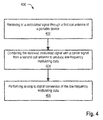
- FIG. 4 shows an example process chart 400 illustrating an example method for enhancing range and increasing of data rates during NFC related functions or transactions.
- the order in which the method is described is not intended to be construed as a limitation, and any number of the described method blocks can be combined in any order to implement the method, or alternate method. Additionally, individual blocks may be deleted from the method without departing from the spirit and scope of the subject matter described herein. Furthermore, the method may be implemented in any suitable hardware, software, firmware, or a combination thereof, without departing from the scope of the invention.
- receiving of a modulated signal through a first coil antenna of a portable device is performed.
- the portable device 102 engages in NFC transaction with the credit card 106 by directing the credit card 106 to the direction of the coverage area of one coil antenna (e.g., first coil antenna 104-2) of the portable device 102.
- the first coil antenna 104-2 of the receiving portable device 102 may operate at a carrier frequency signal of 13.56MHz, which is modulated by a low-frequency data signal from the credit card 106 during the NFC transaction.
- combining the received modulated data with a carrier signal from a second coil antenna of the portable device is performed.
- combining the received modulated data with the carrier signal from another coil antenna may provide sum and difference signals.
- the difference signal may contain the data because the carrier signal is eliminated in the process.
- the receiving portable device 110 may not physically include the second coil antenna 104-4; however, however, its electrical equivalence such as the lumped inductance may be used as the second coil antenna 104-4.
- the combination may provide the same output of producing the data after the carrier signal is cancelled in the process.
- performing an analog to digital conversion is performed.
- the data signal may pass through a receiving pin of the NFC module 202 before the data signal is supplied as an input to the ADC 204.
- the ADC 204 may not require higher resolution such as in 12-bit ADCs. Instead, a similar 4-bit ADC 204 may provide higher data rates and longer range as well.
Landscapes
- Engineering & Computer Science (AREA)
- Computer Networks & Wireless Communication (AREA)
- Signal Processing (AREA)
- Near-Field Transmission Systems (AREA)
Abstract
Description
- A typical wireless communication and power transfer schemes in use today employ inductive coupling between a resonant first coil antenna and a resonant second coil antenna. For example, the wireless communication includes near field communications (NFC) related functions or Europay, MasterCard and Visa (EMVCO) based contactless payment and wireless charging.
- In devices that use NFC for data transfer, there is a mode of operation where a power for the operation of a passive tag is derived from a reader, in addition to the communication link. This mode of operation uses a strong carrier signal to power a tag and simultaneously tries to listen to a load modulated signal from the tag. In this regard, there may be a 50 to 60 dB difference in magnitude of the strong carrier signal and the faint load modulated signal that must be handled by a receiver of the device.
- The above described setup places a lot of design stress on a dynamic range required for an analog to digital converter (ADC). Currently, a high dynamic range such as a 12-bit ADC handles this design stress. However, the 12-bit ADC may only be sampled at a lower rate than a lower resolution ADC.
- The detailed description is described with reference to accompanying figures. In the figures, the left-most digit(s) of a reference number identifies the figure in which the reference number first appears. The same numbers are used throughout the drawings to reference like features and components.
-
FIG. 1 is an example scenario illustrating a near field communication (NFC) coupling arrangement to implement enhanced range and increased data rates during NFC related functions or transactions. -
FIG. 2 is an example apparatus that is configured to implement higher data rates and to enhance further the range during near field communication (NFC) related functions or transactions. -
FIG. 3 is an example system that illustrates carrier signal cancellation scheme in a single coil antenna scenario as described in present implementations herein. -
FIG. 4 is an example process chart illustrating an example method for enhancing range and increasing of data rates during near field communications (NFC) related functions or transactions. - Described herein are architectures, platforms and methods for increasing data rates and to enhance range during NFC related functions or transactions.
- In an implementation, a first coil antenna and a second coil antenna of a portable device are connected in series and are further disposed within the portable device to avoid presence of linkages between the two. In this implementation, the receiving of a modulated signal through the first coil antenna is not affected by a carrier signal or an operating frequency that is present at the second coil antenna, or vice versa.
- With the received modulated data (e.g., through the first coil antenna), an NFC module may be configured to subtract the carrier signal at the second coil antenna from the received modulated data. The subtraction eliminates the carrier signal in the received modulated data and as such, a low-frequency modulating data is produced as a result.
- In an implementation, the low-frequency modulating data is fed to an analog to digital converter (ADC) to transform the modulating data from an analog to a digital signal. In this implementation, the ADC may not require a higher resolution feature as the carrier signal is already cancelled prior to the ADC processing. In other words, the dynamic range requirements at the receiver side of the portable device may be substantially reduced by using, for example, a lower resolution ADC
-
FIG. 1 is anexample scenario 100 that illustrates an NFC coupling arrangement as described in implementations herein. For example, the NFC coupling arrangement demonstrates a particular implementation for obtaining higher data rates and an increase in range during NFC related functions or transactions between devices. -
Scenario 100 may include aportable device 102 with a first coil antenna 104-2 and a second coil antenna 104-4. Thescenario 100 further shows aportable device 102 in near field coupling arrangement with a credit card 106 (e.g., payment transactions) or an NFC tag 108 (e.g., tag reading). Furthermore, aportable device 110 with an antenna 112 is shown to engage in near field coupling arrangement with the portable device 102 (e.g., NFC communications). - As an example of present implementations herein, the
portable device 102 is utilized for payment transactions (e.g., EMVco transactions) for thecredit card 106. In this example, theportable device 102 establishes near field coupling by aligning either the first coil antenna 104-2 or the second coil antenna 104-4 in the direction and within a certain distance of thecredit card 106. At this certain distance, mutual induction between credit card strips (not shown) and the first or second coil antenna may facilitate data communications between thecredit card 106 and theportable device 102. - Similarly, the
NFC tag 108 and theportable device 110 may establish near field coupling arrangement with theportable device 102 in the same manner described above. Particularly, coil strips (not shown) of theNFC tag 108 or the antenna 112 of theportable device 110 may be positioned at a certain distance to either the first or second coil antenna of theportable device 102 to engage in NFC communications. - In an implementation, the first coil antenna 104-2 and the second coil antenna 104-2 of the
portable device 102 may be connected in series and are disposed in a manner to avoid presence of flux linkages between the two. For example, the first coil antenna 104-2 may be disposed on a display side and faces a user (not shown) while the second coil antenna 104-4 may be disposed at a corner or a back-side of theportable device 102. Other examples such as when the first and second coil antennas are at opposite corners of theportable device 102 may similarly apply as long as there is no flux linkages between the two. - With the setup described above, the NFC related functions or transactions may either be facilitated by the first coil antenna 104-2, or the second coil antenna 104-4. For example, due to the configured physical locations of both coil antennas, directing the
credit card 106 to a coverage area of the first coil antenna 104-2 may facilitate the NFC related transaction between the two. In this example, the second coil antenna 104-4, which may be disposed at another end of theportable device 102, may not be a factor to this NFC related transaction. Similarly, the NFC related transaction may be made between thecredit card 106 and the second coil antenna 104-4. At this setup, the first coil antenna 104-2 may be a non-factor during the process as described above. - In the implementation described in the foregoing, the NFC related transaction may utilize a modulated signal to transmit data. For example, in the NFC related transaction between the first coil antenna 104-2 and the
credit card 106, the first coil antenna 104-2 is configured to have an operating frequency of 13.56 MHz. In this example, the operating frequency of 13.56 MHz is a carrier signal that is modulated by data from thecredit card 106 to produce the modulated signal at the first coil antenna 104-2. - In an implementation, an NFC module (not shown) may combine the received modulated signal from the first coil antenna 104-2 with a carrier signal (not shown) that is present in the second coil antenna 104-4, or vice-versa. That is, the NFC module may combine the received modulated signal from the second coil antenna 104-4 with the carrier signal from the first coil antenna 104-2.
- Due to this combination of the modulated signal and the carrier signal, the carrier signal is cancelled to provide low-frequency data. In an implementation, the low-frequency data is fed to one receiving pin (not shown) of the NFC module before they are further converted to digital data by an analog to digital converter (ADC) (not shown). In this example, the ADC may not require higher resolution feature as the carrier signal is already cancelled prior to the ADC processing. In other words, the dynamic range requirements at the receiver side may be substantially reduced by using, for example, a lower resolution ADC.
- The
portable devices -
FIG. 2 illustrates anexample apparatus 200 that is configured to implement higher data rates and to enhance further the range during the near field coupling transactions. Theapparatus 200, for example, is integrated to theportable device 102. As shown, theapparatus 200 includes the first and second coil antennas 104-2 and 104-4, anNFC module 202, an ADC 204, and processor(s) 206. Further shown below the apparatus is agraph 208 for the received modulated signal, agraph 210 for a carrier signal, and agraph 212 for the combined signal to obtain the low-frequency modulating data as further discussed below. - During the NFC related function or transaction, for example, between the
credit card 106 and the first coil antenna 104-2, the received modulated signal is shown by thegraph 208. The received modulated signal at the first coil antenna 104-2 may include an NFC carrier signal of 13.56MHz, and the sideband signals (i.e., 13.56MHz +.847MHz and 13. 56MHz - .847MHz). - As discussed above, the series connected second coil antenna 104-4 is disposed to avoid flux linkages with the first coil antenna 104-2. As such, the second coil antenna 104-4 may provide no effect to the received modulated signal as shown in
graph 208. In other words, the second coil antenna 104-4 may carry or include the operating frequency of 13.56MHz regardless of the present operation or NFC transaction at the first coil antenna 104-2. In this setup, theNFC module 202 may be configured to combine or subtract the carrier signal present in the second coil antenna 104-4 from the received modulated signal in the first coil antenna 104-2. The carrier signal as shown by thegraph 210 is not a modulated signal, but a plain carrier frequency of 13.56 MHz for NFC communications. - With the combined signal, the
graph 212 is produced. Thegraph 212, for example, includes the low-frequency modulating data transmitted through the modulated signal. In other words, the combination of thegraphs NFC module 202 prior to the processing of the low-frequency data signal by theADC 204. - In an implementation, the
ADC 204 may not require high resolution type of ADC. For example, a 4-bit ADC rather than a 12-bit ADC may similarly provide higher data rates and increase in NFC communication range during the NFC related functions or transactions. In this example, the processor(s) may include a software, firmware, hardware, software, or a combination thereof, to control the operation of theapparatus 200. - In other implementations, the first coil antenna or the second coil antenna may be replaced with an equivalent lumped inductor. For example, rather than using a continuous loop of coil antenna in the second coil antenna 104-4, similar results as described above may be obtained if the second coil antenna 104-4 is replaced with a lumped inductor. In this example, a miniaturization of the portable device may be further implemented as well using this design.
- With continuing reference to
FIG. 2 , theNFC module 202 may include a transceiver circuitry that processes electrical signals (not shown) that may be received through the first coil antenna 104-2 or the second coil antenna 104-4. For example, theNFC module 202 may facilitate tuning of the first coil antenna 104-2 for maximum power transfer during transmit or receive operations. In an implementation, theNFC module 202 may be integrated with the first and second coil antennas and/or theprocessor 206 to form a single module. -
FIG. 3 illustrates anexample system 300 that illustrates carrier signal cancellation scheme in a single coil antenna scenario. - As shown, the
example system 300 shows acarrier signal 302 that supplies a carrier signal across the first coil antenna 104-2 and acoupling circuit 304, which may be a lumped inductor that is connected in series with the first coil antenna 104-2. - When a
strip coil 306 of thecredit card 106 enters the coverage area of the first coil antenna 104-2, mutual induction may facilitate modulation of the carrier signal across the first coil antenna 104-2. For example, the modulated signal as shown ingraph 208 ofFig. 2 may be derived when thestrip coil 306 engages in NFC transaction with the first coil antenna 104-2. - For the
coupling circuit 304, an undisturbed carrier signal similar to thegraph 210 may be derived. For example, thecarrier signal 302 supplies an operating frequency of 13.56 MHz for NFC communications. In this example, the 13.56 MHz carrier signal is unperturbed by the present NFC communications between the first coil antenna 104-2 and thecredit card 106 because thecoupling circuit 304 is disposed in a physical location to avoid flux linkages with the first coil antenna 104-2. - In an implementation, an
output 308 may include thegraph 212 as shown inFig. 2 . That is, the signal across the first coil antenna 104-2 and the signal across thecoupling circuit 304 are combined to eliminate the 13.56 MHz carrier signal. In this implementation, the low-frequency data in theoutput 308 may then be fed at the receiving pin of theNFC module 202 for further processing such as, by theADC 204. - In other implementations, additional isolation between the first coil antenna 104-2 and the coupling circuit 304 (or the second coil antenna 104-4) may be obtained by feeding them through a splitter rather than directly from, for example, a driver of an NFC chip. In this implementation, the splitting and subsequent subtraction (i.e., combination of modulated and carrier signals) may be implemented through a lumped element implementation of a 180 degree hybrid.
- For example, the lumped 180 degree hybrid (not shown) includes four ports. In this example, ports 2 and 3 receive the carrier signal while
port 1 and 4 provides sum and difference of signals, respectively. The sum may be used during transmission while the difference signal may go to a receiver circuitry of the portable device. -
FIG. 4 shows anexample process chart 400 illustrating an example method for enhancing range and increasing of data rates during NFC related functions or transactions. The order in which the method is described is not intended to be construed as a limitation, and any number of the described method blocks can be combined in any order to implement the method, or alternate method. Additionally, individual blocks may be deleted from the method without departing from the spirit and scope of the subject matter described herein. Furthermore, the method may be implemented in any suitable hardware, software, firmware, or a combination thereof, without departing from the scope of the invention. - At
block 402, receiving of a modulated signal through a first coil antenna of a portable device is performed. For example, theportable device 102 engages in NFC transaction with thecredit card 106 by directing thecredit card 106 to the direction of the coverage area of one coil antenna (e.g., first coil antenna 104-2) of theportable device 102. In this example, the first coil antenna 104-2 of the receivingportable device 102 may operate at a carrier frequency signal of 13.56MHz, which is modulated by a low-frequency data signal from thecredit card 106 during the NFC transaction. - At
block 404, combining the received modulated data with a carrier signal from a second coil antenna of the portable device is performed. For example, combining the received modulated data with the carrier signal from another coil antenna (e.g., second coil antenna 104-4) may provide sum and difference signals. In this example, the difference signal may contain the data because the carrier signal is eliminated in the process. - In another example, the receiving
portable device 110 may not physically include the second coil antenna 104-4; however, however, its electrical equivalence such as the lumped inductance may be used as the second coil antenna 104-4. In this other example, the combination may provide the same output of producing the data after the carrier signal is cancelled in the process. - At
block 406, performing an analog to digital conversion is performed. With the obtained output data signal from the difference signal atblock 404, the data signal may pass through a receiving pin of theNFC module 202 before the data signal is supplied as an input to theADC 204. In this example, theADC 204 may not require higher resolution such as in 12-bit ADCs. Instead, a similar 4-bit ADC 204 may provide higher data rates and longer range as well. - The following examples pertain to further embodiments:
- Example 1 is a device comprising: a near field communication (NFC) module; a first coil antenna coupled to the NFC module, the first coil antenna configured to receive a modulated signal; a second coil antenna coupled to the NFC module and connected in series with the first coil antenna, the second coil antenna configured to provide a carrier signal that is combined with the received modulated signal to produce data; and an analog to digital converter (ADC) configured to receive and transform the data from an analog to a digital signal.
- In example 2, the device as recited in example 1, wherein the NFC module further includes a receiving pin configured to receive the data before supplying the data to the ADC.
- In example 3, the device as recited in example 1, wherein the carrier signal provided by the second coil antenna is configured to operate an operating frequency of about 13.56 MHz, which is combined with the received modulated signal to remove the carrier signal from the received modulated signal.
- In example 4, the device as recited in example 1, wherein the second coil antenna is a lumped inductor.
- In example 5, the device as recited in example 1, wherein the first coil antenna is disposed at front side of the device while the second coil antenna is disposed at a back side of the device.
- In example 6, the device as recited in any of examples 1 to 5, wherein there is minimal flux linkage between the first coil antenna and the second coil antenna.
- In example 7, the device as recited in any of examples 1 to 5, wherein the first coil antenna is configured to operate independently from the second coil antenna.
- Example 8 is an apparatus comprising: a first coil antenna configured to receive a modulated signal; a lumped inductor configured to produce a carrier signal that is combined with the modulated signal to obtain data signal; and an analog to digital converter (ADC) configured to transform the data signal from an analog data signal into a digital data signal.
- In example 9, the apparatus as recited in example 8, wherein there is minimal flux linkage between the first coil antenna and the lumped inductor.
- In example 10, the apparatus as recited in example 8, wherein the first coil antenna comprises a continuous loop of coil antenna configured to operate at a carrier frequency of about 13.56 MHz for near field coupling (NFC) communications.
- In example 11, the apparatus as recited in example 8, wherein the carrier signal provided by the lumped inductor includes an operating frequency of about 13.56 MHz, which is combined with the received modulated signal to remove the carrier signal from the received modulated signal.
- In example 12, the apparatus as recited in example 8, wherein the first coil antenna is disposed at front side of a device while the lumped inductor is disposed at a back side of the device.
- In example 13, the apparatus as recited in example 8 further comprising a 180 degree hybrid splitter configured to isolate the first coil antenna from the lumped inductor.
- In example 14, the apparatus as recited in any of examples 8 to 13, wherein the first coil antenna is configured to operate independently from the lumped inductor.
- Example 15 is a method of enhancing range and increasing of data rates during near field communications (NFC) related functions or transactions in a device, the method comprising: receiving of a modulated signal by a first coil antenna; combining the received modulated signal to a carrier signal produced by a second coil antenna, wherein the combining cancels the carrier signal of the received modulated signal to provide a data signal; and performing an analog to digital conversion of the data signal.
- In example 16, the method as recited in example 15, wherein there is minimal flux linkage between the first coil antenna and the second coil antenna.
- In example 17, the method as recited in example 15, wherein the carrier signal provided by the second coil antenna includes an operating frequency of about 13.56 MHz for NFC communications.
- In example 18, the method as recited in example 15, wherein the second coil antenna is a lumped inductor.
- In example 19, the method as recited in example 15, wherein the first coil antenna is operated independently from the second coil antenna.
- In example 20, the method as recited in any of examples 15 to 19, wherein the data signal is a low-frequency data signal.
Claims (13)
- A device comprising:a near field communication (NFC) module;a first coil antenna coupled to the NFC module, the first coil antenna configured to receive a modulated signal;a second coil antenna coupled to the NFC module and connected in series with the first coil antenna, the second coil antenna configured to provide a carrier signal that is combined with the received modulated signal to produce data; andan analog to digital converter (ADC) configured to receive and transform the data from an analog to a digital signal.
- The device as recited in claim 1, wherein the NFC module further includes a receiving pin configured to receive the data before supplying the data to the ADC.
- The device as recited in claim 1, wherein there is minimal flux linkage between the first coil antenna and the second coil antenna.
- The device as recited in claim 1, wherein the carrier signal provided by the second coil antenna is configured to operate an operating frequency of about 13.56 MHz, which is combined with the received modulated signal to remove the carrier signal from the received modulated signal.
- The device as recited in claim 1, wherein the second coil antenna is a lumped inductor.
- The device as recited in claim 1, wherein the first coil antenna is configured to operate independently from the second coil antenna.
- The device as recited in claim 1, wherein the first coil antenna is disposed at front side of the device while the second coil antenna is disposed at a back side of the device.
- A method of enhancing range and increasing of data rates during near field communications (NFC) related functions or transactions in a device, the method comprising:receiving of a modulated signal by a first coil antenna;combining the received modulated signal to a carrier signal produced by a second coil antenna, wherein the combining comprises canceling the carrier signal of the received modulated signal to provide a data signal; andperforming an analog to digital conversion of the data signal.
- The method as recited in claim 8, wherein there is minimal flux linkage between the first coil antenna and the second coil antenna.
- The method as recited in claim 8, wherein the carrier signal provided by the second coil antenna includes an operating frequency of about 13.56 MHz for NFC communications.
- The method as recited in claim 8, wherein the second coil antenna is a lumped inductor.
- The method as recited in claim 8, wherein the first coil antenna is operated independently from the second coil antenna.
- The method as recited in claim 8, wherein the data signal is a low-frequency data signal.
Applications Claiming Priority (1)
| Application Number | Priority Date | Filing Date | Title |
|---|---|---|---|
| US14/572,050 US9848281B2 (en) | 2014-12-16 | 2014-12-16 | Enhancing data rate or range of near field communication using differential coil topology |
Publications (1)
| Publication Number | Publication Date |
|---|---|
| EP3035553A1 true EP3035553A1 (en) | 2016-06-22 |
Family
ID=54704966
Family Applications (1)
| Application Number | Title | Priority Date | Filing Date |
|---|---|---|---|
| EP15193983.2A Withdrawn EP3035553A1 (en) | 2014-12-16 | 2015-11-10 | Enhancing data rate or range of near field communication using differential coil topology |
Country Status (3)
| Country | Link |
|---|---|
| US (1) | US9848281B2 (en) |
| EP (1) | EP3035553A1 (en) |
| CN (1) | CN105703804B (en) |
Cited By (1)
| Publication number | Priority date | Publication date | Assignee | Title |
|---|---|---|---|---|
| CN108631043A (en) * | 2017-03-24 | 2018-10-09 | 国民技术股份有限公司 | A kind of NFC antenna and terminal |
Families Citing this family (3)
| Publication number | Priority date | Publication date | Assignee | Title |
|---|---|---|---|---|
| CN107612578A (en) * | 2017-10-24 | 2018-01-19 | 深圳市前海胜马科技有限公司 | Near-field communication equipment |
| CN111601295B (en) * | 2020-07-22 | 2020-10-23 | 深圳Tcl新技术有限公司 | Method, system, device and readable storage medium for dynamically adjusting transmission rate |
| CN118095331B (en) * | 2024-02-08 | 2025-07-04 | 支付宝(杭州)信息技术有限公司 | Electronic device, NFC-based communication method and system |
Citations (2)
| Publication number | Priority date | Publication date | Assignee | Title |
|---|---|---|---|---|
| US5847662A (en) * | 1994-12-27 | 1998-12-08 | Kabushiki Kaisha Toshiba | Radio card communication apparatus |
| US20100318315A1 (en) * | 2007-07-05 | 2010-12-16 | Patrik Smets | Method and system for simulating a proximity-based transaction device |
Family Cites Families (12)
| Publication number | Priority date | Publication date | Assignee | Title |
|---|---|---|---|---|
| US6744883B1 (en) * | 1999-01-12 | 2004-06-01 | Paradyne Corporation | Filter system and method to suppress interference imposed upon a frequency-division multiplexed channel |
| US8502675B2 (en) * | 2002-09-23 | 2013-08-06 | Lord Corporation | Remotely powered and remotely interrogated wireless digital sensor telemetry system to detect corrosion |
| US7705773B2 (en) * | 2005-12-19 | 2010-04-27 | Honeywell International Inc. | Self-calibrating a radar altimeter based on a simulated return signal |
| EP2511977A1 (en) * | 2011-04-15 | 2012-10-17 | Gemalto SA | Arrangement of antennas emitting and receiving an electromagnetic field |
| US9448297B2 (en) * | 2011-09-07 | 2016-09-20 | Koninklijke Philips N.V. | Mode splitter/combiner for noise figure minimization and control of power in RF coil arrays |
| KR101851590B1 (en) * | 2011-11-28 | 2018-04-25 | 삼성전자주식회사 | Wireless power transmission system and multi mode resonator in wireless power transmission system |
| CN103515704A (en) * | 2012-06-27 | 2014-01-15 | 比亚迪股份有限公司 | Near field communication antenna and electronic equipment |
| US9654184B2 (en) * | 2012-07-20 | 2017-05-16 | WIPQTUS Inc. | Transmitter to receiver communication link in a wireless power system |
| US9143200B2 (en) * | 2012-09-26 | 2015-09-22 | Qualcomm Incorporated | Apparatus and method of receiver architecture and low-complexity decoder for line-coded and amplitude-modulated signal |
| CN103413165B (en) * | 2013-08-07 | 2017-08-25 | 歌尔股份有限公司 | Control the method and controlled NFC label of NFC label |
| CN203800175U (en) * | 2014-05-14 | 2014-08-27 | 惠州硕贝德无线科技股份有限公司 | NFC antenna module |
| CN204009990U (en) * | 2014-08-28 | 2014-12-10 | 黄�俊 | A kind of flexible multi-layered compound NFC passive label paster with LED lamp |
-
2014
- 2014-12-16 US US14/572,050 patent/US9848281B2/en not_active Expired - Fee Related
-
2015
- 2015-11-10 EP EP15193983.2A patent/EP3035553A1/en not_active Withdrawn
- 2015-11-16 CN CN201510783389.6A patent/CN105703804B/en not_active Expired - Fee Related
Patent Citations (2)
| Publication number | Priority date | Publication date | Assignee | Title |
|---|---|---|---|---|
| US5847662A (en) * | 1994-12-27 | 1998-12-08 | Kabushiki Kaisha Toshiba | Radio card communication apparatus |
| US20100318315A1 (en) * | 2007-07-05 | 2010-12-16 | Patrik Smets | Method and system for simulating a proximity-based transaction device |
Non-Patent Citations (1)
| Title |
|---|
| SHAMELI A ET AL: "An RFID System with Fully Integrated Transponder", RADIO FREQUENCY INTEGRATED CIRCUITS (RFIC) SYMPOSIUM, 2007 IEEE, IEEE, PISCATAWAY, NJ, USA, 1 June 2007 (2007-06-01), pages 285 - 288, XP031113031, ISBN: 978-1-4244-0530-5 * |
Cited By (1)
| Publication number | Priority date | Publication date | Assignee | Title |
|---|---|---|---|---|
| CN108631043A (en) * | 2017-03-24 | 2018-10-09 | 国民技术股份有限公司 | A kind of NFC antenna and terminal |
Also Published As
| Publication number | Publication date |
|---|---|
| US20160174017A1 (en) | 2016-06-16 |
| CN105703804B (en) | 2018-08-28 |
| CN105703804A (en) | 2016-06-22 |
| US9848281B2 (en) | 2017-12-19 |
Similar Documents
| Publication | Publication Date | Title |
|---|---|---|
| US8725088B2 (en) | Antenna solution for near-field and far-field communication in wireless devices | |
| CN103218644B (en) | A kind of super high frequency electronic label read/write of carrier wave cancellation | |
| US10361474B2 (en) | Near field communication device | |
| US9692525B2 (en) | Optimal electric field coupling techniques for human body communication (HBC) | |
| US9461716B2 (en) | Near field communications (NFC) modulation feedback apparatus for tuned antenna configurations | |
| CN109088657B (en) | RF front-end module and near field communication device | |
| US11038553B2 (en) | EMC inductor-free RF front-end method and topology with power by field function for an inductively coupled communication system | |
| KR101938650B1 (en) | Near-Field Wireless Transceiver Circuit and Mobile Terminal | |
| US9408015B2 (en) | Reducing receiver performance degradation due to frequency coexistence | |
| US9848281B2 (en) | Enhancing data rate or range of near field communication using differential coil topology | |
| EP2388930A2 (en) | Overvoltage protection in a near field communications (NFC) capable device | |
| WO2019204988A1 (en) | Near field communication antenna system and terminal device | |
| US9042822B2 (en) | Communication device and near field communication circuit thereof | |
| CN106203222A (en) | It is applied to the echo canceling method of remote UHF rfid interrogator | |
| CN103295036A (en) | Phase-locked carrier wave cancellation ultrahigh-frequency radio frequency identification reader and cancellation method thereof | |
| EP2713524A2 (en) | Remote antenna driver for reducing unwanted electromagnetic emissions and/or distortion within a near field communication (NFC) capable device | |
| CN101159024A (en) | Semiconductor integrated circuit device and receiving device | |
| US11025347B2 (en) | Compensating for channel distortion during contactless communication | |
| US10476555B2 (en) | Chassis based antenna for a near field communication (NFC) enabled device | |
| CN109951200A (en) | Electronic equipment and electronic system | |
| CN204993871U (en) | System and contactless communication device for contactless communication of information | |
| CN204993318U (en) | Near field communications received circuit | |
| CN105634511A (en) | A circuit system and mobile terminal for sharing antenna between NFC and WIFI | |
| Finkenzeller et al. | Range extension of an ISO/IEC 14443 type a RFID system with actively emulating load modulation | |
| US20250385709A1 (en) | Digital leakage canceling device of rfid reader and method thereof |
Legal Events
| Date | Code | Title | Description |
|---|---|---|---|
| PUAI | Public reference made under article 153(3) epc to a published international application that has entered the european phase |
Free format text: ORIGINAL CODE: 0009012 |
|
| 17P | Request for examination filed |
Effective date: 20151110 |
|
| AK | Designated contracting states |
Kind code of ref document: A1 Designated state(s): AL AT BE BG CH CY CZ DE DK EE ES FI FR GB GR HR HU IE IS IT LI LT LU LV MC MK MT NL NO PL PT RO RS SE SI SK SM TR |
|
| AX | Request for extension of the european patent |
Extension state: BA ME |
|
| RIN1 | Information on inventor provided before grant (corrected) |
Inventor name: YANG, SONGNAN Inventor name: KONANUR, ANAND S. Inventor name: AGIS, EDWARD Inventor name: KARANDIKAR, NIRANJAN Inventor name: KARACAOGLU, ULUN |
|
| 17Q | First examination report despatched |
Effective date: 20180928 |
|
| GRAP | Despatch of communication of intention to grant a patent |
Free format text: ORIGINAL CODE: EPIDOSNIGR1 |
|
| STAA | Information on the status of an ep patent application or granted ep patent |
Free format text: STATUS: GRANT OF PATENT IS INTENDED |
|
| RIC1 | Information provided on ipc code assigned before grant |
Ipc: H04B 5/00 20060101AFI20200507BHEP Ipc: H04W 4/80 20180101ALI20200507BHEP |
|
| INTG | Intention to grant announced |
Effective date: 20200609 |
|
| STAA | Information on the status of an ep patent application or granted ep patent |
Free format text: STATUS: THE APPLICATION IS DEEMED TO BE WITHDRAWN |
|
| 18D | Application deemed to be withdrawn |
Effective date: 20201020 |