EP3034314A1 - Security chip against counterfeiting, especially banknotes - Google Patents
Security chip against counterfeiting, especially banknotes Download PDFInfo
- Publication number
- EP3034314A1 EP3034314A1 EP14460115.0A EP14460115A EP3034314A1 EP 3034314 A1 EP3034314 A1 EP 3034314A1 EP 14460115 A EP14460115 A EP 14460115A EP 3034314 A1 EP3034314 A1 EP 3034314A1
- Authority
- EP
- European Patent Office
- Prior art keywords
- chip
- graphene
- layer
- security chip
- security
- Prior art date
- Legal status (The legal status is an assumption and is not a legal conclusion. Google has not performed a legal analysis and makes no representation as to the accuracy of the status listed.)
- Withdrawn
Links
Images



Classifications
-
- G—PHYSICS
- G06—COMPUTING OR CALCULATING; COUNTING
- G06Q—INFORMATION AND COMMUNICATION TECHNOLOGY [ICT] SPECIALLY ADAPTED FOR ADMINISTRATIVE, COMMERCIAL, FINANCIAL, MANAGERIAL OR SUPERVISORY PURPOSES; SYSTEMS OR METHODS SPECIALLY ADAPTED FOR ADMINISTRATIVE, COMMERCIAL, FINANCIAL, MANAGERIAL OR SUPERVISORY PURPOSES, NOT OTHERWISE PROVIDED FOR
- G06Q30/00—Commerce
- G06Q30/018—Certifying business or products
- G06Q30/0185—Product, service or business identity fraud
-
- B—PERFORMING OPERATIONS; TRANSPORTING
- B42—BOOKBINDING; ALBUMS; FILES; SPECIAL PRINTED MATTER
- B42D—BOOKS; BOOK COVERS; LOOSE LEAVES; PRINTED MATTER CHARACTERISED BY IDENTIFICATION OR SECURITY FEATURES; PRINTED MATTER OF SPECIAL FORMAT OR STYLE NOT OTHERWISE PROVIDED FOR; DEVICES FOR USE THEREWITH AND NOT OTHERWISE PROVIDED FOR; MOVABLE-STRIP WRITING OR READING APPARATUS
- B42D25/00—Information-bearing cards or sheet-like structures characterised by identification or security features; Manufacture thereof
- B42D25/30—Identification or security features, e.g. for preventing forgery
- B42D25/305—Associated digital information
-
- B—PERFORMING OPERATIONS; TRANSPORTING
- B42—BOOKBINDING; ALBUMS; FILES; SPECIAL PRINTED MATTER
- B42D—BOOKS; BOOK COVERS; LOOSE LEAVES; PRINTED MATTER CHARACTERISED BY IDENTIFICATION OR SECURITY FEATURES; PRINTED MATTER OF SPECIAL FORMAT OR STYLE NOT OTHERWISE PROVIDED FOR; DEVICES FOR USE THEREWITH AND NOT OTHERWISE PROVIDED FOR; MOVABLE-STRIP WRITING OR READING APPARATUS
- B42D25/00—Information-bearing cards or sheet-like structures characterised by identification or security features; Manufacture thereof
- B42D25/30—Identification or security features, e.g. for preventing forgery
- B42D25/36—Identification or security features, e.g. for preventing forgery comprising special materials
-
- G—PHYSICS
- G06—COMPUTING OR CALCULATING; COUNTING
- G06K—GRAPHICAL DATA READING; PRESENTATION OF DATA; RECORD CARRIERS; HANDLING RECORD CARRIERS
- G06K19/00—Record carriers for use with machines and with at least a part designed to carry digital markings
- G06K19/02—Record carriers for use with machines and with at least a part designed to carry digital markings characterised by the selection of materials, e.g. to avoid wear during transport through the machine
- G06K19/025—Record carriers for use with machines and with at least a part designed to carry digital markings characterised by the selection of materials, e.g. to avoid wear during transport through the machine the material being flexible or adapted for folding, e.g. paper or paper-like materials used in luggage labels, identification tags, forms or identification documents carrying RFIDs
-
- G—PHYSICS
- G06—COMPUTING OR CALCULATING; COUNTING
- G06K—GRAPHICAL DATA READING; PRESENTATION OF DATA; RECORD CARRIERS; HANDLING RECORD CARRIERS
- G06K19/00—Record carriers for use with machines and with at least a part designed to carry digital markings
- G06K19/06—Record carriers for use with machines and with at least a part designed to carry digital markings characterised by the kind of the digital marking, e.g. shape, nature, code
- G06K19/06009—Record carriers for use with machines and with at least a part designed to carry digital markings characterised by the kind of the digital marking, e.g. shape, nature, code with optically detectable marking
- G06K19/06046—Constructional details
- G06K19/06112—Constructional details the marking being simulated using a light source, e.g. a barcode shown on a display or a laser beam with time-varying intensity profile
-
- G—PHYSICS
- G06—COMPUTING OR CALCULATING; COUNTING
- G06K—GRAPHICAL DATA READING; PRESENTATION OF DATA; RECORD CARRIERS; HANDLING RECORD CARRIERS
- G06K19/00—Record carriers for use with machines and with at least a part designed to carry digital markings
- G06K19/06—Record carriers for use with machines and with at least a part designed to carry digital markings characterised by the kind of the digital marking, e.g. shape, nature, code
- G06K19/067—Record carriers with conductive marks, printed circuits or semiconductor circuit elements, e.g. credit or identity cards also with resonating or responding marks without active components
- G06K19/07—Record carriers with conductive marks, printed circuits or semiconductor circuit elements, e.g. credit or identity cards also with resonating or responding marks without active components with integrated circuit chips
- G06K19/077—Constructional details, e.g. mounting of circuits in the carrier
- G06K19/07749—Constructional details, e.g. mounting of circuits in the carrier the record carrier being capable of non-contact communication, e.g. constructional details of the antenna of a non-contact smart card
-
- G—PHYSICS
- G06—COMPUTING OR CALCULATING; COUNTING
- G06K—GRAPHICAL DATA READING; PRESENTATION OF DATA; RECORD CARRIERS; HANDLING RECORD CARRIERS
- G06K7/00—Methods or arrangements for sensing record carriers, e.g. for reading patterns
- G06K7/10—Methods or arrangements for sensing record carriers, e.g. for reading patterns by electromagnetic radiation, e.g. optical sensing; by corpuscular radiation
- G06K7/10009—Methods or arrangements for sensing record carriers, e.g. for reading patterns by electromagnetic radiation, e.g. optical sensing; by corpuscular radiation sensing by radiation using wavelengths larger than 0.1 mm, e.g. radio-waves or microwaves
- G06K7/10316—Methods or arrangements for sensing record carriers, e.g. for reading patterns by electromagnetic radiation, e.g. optical sensing; by corpuscular radiation sensing by radiation using wavelengths larger than 0.1 mm, e.g. radio-waves or microwaves using at least one antenna particularly designed for interrogating the wireless record carriers
- G06K7/10326—Methods or arrangements for sensing record carriers, e.g. for reading patterns by electromagnetic radiation, e.g. optical sensing; by corpuscular radiation sensing by radiation using wavelengths larger than 0.1 mm, e.g. radio-waves or microwaves using at least one antenna particularly designed for interrogating the wireless record carriers the antenna being of the very-near field type, e.g. capacitive
-
- G—PHYSICS
- G07—CHECKING-DEVICES
- G07D—HANDLING OF COINS OR VALUABLE PAPERS, e.g. TESTING, SORTING BY DENOMINATIONS, COUNTING, DISPENSING, CHANGING OR DEPOSITING
- G07D7/00—Testing specially adapted to determine the identity or genuineness of valuable papers or for segregating those which are unacceptable, e.g. banknotes that are alien to a currency
- G07D7/004—Testing specially adapted to determine the identity or genuineness of valuable papers or for segregating those which are unacceptable, e.g. banknotes that are alien to a currency using digital security elements, e.g. information coded on a magnetic thread or strip
-
- G—PHYSICS
- G07—CHECKING-DEVICES
- G07D—HANDLING OF COINS OR VALUABLE PAPERS, e.g. TESTING, SORTING BY DENOMINATIONS, COUNTING, DISPENSING, CHANGING OR DEPOSITING
- G07D7/00—Testing specially adapted to determine the identity or genuineness of valuable papers or for segregating those which are unacceptable, e.g. banknotes that are alien to a currency
- G07D7/01—Testing electronic circuits therein
Definitions
- the invention relates to a security chip against counterfeiting, especially for banknotes and other documents (e.g. pre-numbered forms), enabling the verification of the authenticity of a document.
- banknotes In the production of banknotes complex printing techniques are used. Thanks to securities it is easy to distinguish a genuine banknote from a counterfeit one. The authenticity of a banknote can be tested by checking the securities visible to the naked eye (e.g. a watermark, a hologram), tactile (stiff and rustling paper, printing convex in some places) and securities visible under UV light.
- Euro banknotes also have a number of hidden securities detected by sensors in vending machines or high-performance sorting machines used by central banks. The most sophisticated hidden securities can be verified only with the help of advanced sensors, only available to central banks. These sensors are produced only by a few companies. Thanks to them, even if a commercial bank or retail business transferred counterfeit money to the central bank, their return to the circuit would be highly unlikely.
- the aim of the present invention is therefore to provide a new kind of security.
- the invention is a chip securing against counterfeiting, in particular banknotes, characterized in that it comprises an electronic circuit disposed on elastic layer of nanocomposite graphene material, comprising an antenna, an electroluminescent element and preferably also an electromotive force processing chip adapted to process the signal received by the DC powered security chip powering the electroluminescent element, wherein the elastic layer of graphene nanocomposite material comprises at least one graphene layer disposed on the adhesive layer, preferably a polymer.
- the chip comprises a capacitive touch switch configured to close the circuit chip by a finger touching the contacts.
- the switch contacts are led to the surface of at least one layer of adhesive.
- At least one component of the security chip, and preferably each component of the chip, is made of graphene, and is an integral part of the flexible layer of graphene nanocomposite material.
- the chip is designed to be excited by a GSM signal in the frequency range from 900 MHz to 2,100 MHz.
- graphene is present in pure or doped form.
- the chip comprises a layer of graphene, and two adhesive layers, wherein the graphene layer is located directly between the two layers of adhesive.
- graphene is in a two-dimensional form having a thickness of one atom or more than one atom or three dimensional and preferably they are nanotubes arranged in different directions, in particular parallel or perpendicular to the surface of the adhesive.
- the invention also includes the use of the chip according to the invention for securing banknotes, holograms, documents, passports, credit cards, excise bands, excise forms, personal identifiers, certificates or product labels.
- the present invention is further a chip for verifying the authenticity of documents, in particular banknotes comprising a security chip according to the invention and a device adapted for generating a signal exciting the chip.
- the apparatus adapted for generating a signal exciting the chip is adapted to record the signal generated by the electroluminescent element.
- the apparatus adapted for generating a signal exciting the chip is a mobile phone.
- the invention also applies to a method for checking the authenticity of documents, in particular banknotes, characterized in that the chip is used according to the invention.
- the security chip is made of a nanocomposite which has a binder as one component, preferably a polymer, which ensures its integrity, hardness, flexibility and resistance to compression, and the second is a monatomic layer of graphene, which provides conductive properties while maintaining the transparency of the material.
- Graphene has all the properties corresponding to the requirements of the production of nanocomposite material for a security chip, for example
- the security chip made with graphene is completely transparent, which allows to use it, for example in the so-called “windows" of polymer banknotes, as the surface layer of a hologram or as an inherent solution to cover any layers requiring protection.
- a source of visible light, polarized light, or UV radiation is an electroluminescent component.
- visible light the end result is a visual effect discernible by a human eye.
- UV light emitting element the end result will be the backlight of fluorescent markers located within the light source.
- polarized light the film or printouts generated by printing, stretching, or stamping will be exposed.
- the chip does not require a constant power supply to achieve the effect of electroluminescence.
- the security chip is made of a composite material resistant to:
- Ease of fitting a polymer nanolayer to the hologram security production process is important because of its ability to adapt to a variety of hologram manufacturing processes, as well as to the application process by hot-stamping or cold-stamping.
- the technological features of the security chip do not restrict the use of any of the mentioned methods.
- the security chip according to the technological modification is not limited by the current circuit designed in the example, the shape and size of the antenna or the selection of the light emitting element meeting the technical requirements, for example limitations on thickness of the structure of a banknote.
- One of the advantages of the security chip according to the invention is also the ease to verify the authenticity of a document secured by this chip, requiring only a device for the excitation of the chip, which may be, for example a mobile phone.
- the security chip (1) is one of the layers of a polymer banknote.
- the security chip in the embodiment is an integral part of the hologram, i.e. is placed on the same layer of the film with a hologram.
- the chip begins to operate by applying an electromagnetic field generated using induced cell phone antenna (6).
- the security chip (1) is tuned in the frequency range of GSM 900 MHz to 2100 MHz.
- a smartphone or a phone working on GSM frequencies (6) is a control instrument inducing the security chip.
- the smartphone using dedicated application short-exciting the embedded antenna generates an electromagnetic field.
- the signal in the electromotive force processing chip (3) is converted to DC and then it powers the electroluminescent element (4), which starts to glow.
- the electroluminescent element (4) glows as long as the source is applied to the electromagnetic field of the security chip (1).
- the application on a smartphone (6) also detects the chip operation (receiving glowing of the electroluminescent element) using a camera. In the event of activation of the chip - the application will notify the user with an additional message about the fact of the chip excitation.
- Application functionality allows one to easily use it and also for a blind person to verify a banknote.
- the chip (1) is made so as to operate capacitively with the circuit closed with a finger (the "touch” option).
- the operation of the capacitive circuits is based on the phenomenon of the impact of the electric field with conductors, in particular the human body, which is filled with electrolytes and surrounded by a conductive layer of lossy dielectric - the skin.
- the electronic component that produces the electric field is a capacitor and as with any capacitor each part of the field goes out the covers. This field is called the boundary field.
- the system of covers in the touch switch is designed so that the field is the greatest and directed to the area available to the user's finger.
- the finger located in the boundary electric field introduces a certain capacity into the chip, which is called touch capacitance (CD).
- Capacitive mode of operation of the security chip is illustrated in Figure 5 .
- the arrangement of graphene nanocomposite structure can take any form that can achieve maximum performance of the security chip during its use.
- the structure of the nanocomposite material security chip takes into account:
- the components of the nanocomposite layer should be made in one of the selected ways:
Landscapes
- Engineering & Computer Science (AREA)
- Physics & Mathematics (AREA)
- General Physics & Mathematics (AREA)
- Theoretical Computer Science (AREA)
- Business, Economics & Management (AREA)
- Toxicology (AREA)
- Health & Medical Sciences (AREA)
- Entrepreneurship & Innovation (AREA)
- Strategic Management (AREA)
- General Business, Economics & Management (AREA)
- Economics (AREA)
- Development Economics (AREA)
- Accounting & Taxation (AREA)
- Marketing (AREA)
- Finance (AREA)
- Microelectronics & Electronic Packaging (AREA)
- Optics & Photonics (AREA)
- Computer Hardware Design (AREA)
- Computer Security & Cryptography (AREA)
- Computer Networks & Wireless Communication (AREA)
- Electromagnetism (AREA)
- General Health & Medical Sciences (AREA)
- Artificial Intelligence (AREA)
- Computer Vision & Pattern Recognition (AREA)
- Credit Cards Or The Like (AREA)
Abstract
wherein the elastic layer graphene nanocomposite material comprises at least one layer of graphene (G) arranged on an adhesive layer, preferably polymer (P).
Description
- The invention relates to a security chip against counterfeiting, especially for banknotes and other documents (e.g. pre-numbered forms), enabling the verification of the authenticity of a document.
- In the production of banknotes complex printing techniques are used. Thanks to securities it is easy to distinguish a genuine banknote from a counterfeit one. The authenticity of a banknote can be tested by checking the securities visible to the naked eye (e.g. a watermark, a hologram), tactile (stiff and rustling paper, printing convex in some places) and securities visible under UV light. Euro banknotes also have a number of hidden securities detected by sensors in vending machines or high-performance sorting machines used by central banks. The most sophisticated hidden securities can be verified only with the help of advanced sensors, only available to central banks. These sensors are produced only by a few companies. Thanks to them, even if a commercial bank or retail business transferred counterfeit money to the central bank, their return to the circuit would be highly unlikely.
- Due to the continuous development of counterfeiting techniques constant search for new methods of document protection against illegal copying is needed. The aim of the present invention is therefore to provide a new kind of security.
- This was achieved by proposing security in the form of an electronic circuit mounted on a flexible layer of composite graphene material. Graphene has all the properties corresponding to the requirements of the production of nanocomposite material for a chip securing, for example electricity conductivity and transparency. Additionally, in the prior art methods are known for manufacturing an electronic circuit structure (
US2012217480 ) and an antenna (US2013004658 ) of graphene. - The invention is a chip securing against counterfeiting, in particular banknotes, characterized in that it comprises an electronic circuit disposed on elastic layer of nanocomposite graphene material, comprising an antenna, an electroluminescent element and preferably also an electromotive force processing chip adapted to process the signal received by the DC powered security chip powering the electroluminescent element, wherein the elastic layer of graphene nanocomposite material comprises at least one graphene layer disposed on the adhesive layer, preferably a polymer.
- Preferably, the chip comprises a capacitive touch switch configured to close the circuit chip by a finger touching the contacts.
- Preferably, the switch contacts are led to the surface of at least one layer of adhesive.
- Preferably, at least one component of the security chip, and preferably each component of the chip, is made of graphene, and is an integral part of the flexible layer of graphene nanocomposite material.
- Preferably, the chip is designed to be excited by a GSM signal in the frequency range from 900 MHz to 2,100 MHz.
- Preferably graphene is present in pure or doped form.
- Preferably, the chip comprises a layer of graphene, and two adhesive layers, wherein the graphene layer is located directly between the two layers of adhesive.
- Preferably graphene is in a two-dimensional form having a thickness of one atom or more than one atom or three dimensional and preferably they are nanotubes arranged in different directions, in particular parallel or perpendicular to the surface of the adhesive.
- The invention also includes the use of the chip according to the invention for securing banknotes, holograms, documents, passports, credit cards, excise bands, excise forms, personal identifiers, certificates or product labels.
- The present invention is further a chip for verifying the authenticity of documents, in particular banknotes comprising a security chip according to the invention and a device adapted for generating a signal exciting the chip.
- Preferably, the apparatus adapted for generating a signal exciting the chip is adapted to record the signal generated by the electroluminescent element.
- Preferably, the apparatus adapted for generating a signal exciting the chip is a mobile phone.
- The invention also applies to a method for checking the authenticity of documents, in particular banknotes, characterized in that the chip is used according to the invention.
- The security chip is made of a nanocomposite which has a binder as one component, preferably a polymer, which ensures its integrity, hardness, flexibility and resistance to compression, and the second is a monatomic layer of graphene, which provides conductive properties while maintaining the transparency of the material.
- Graphene has all the properties corresponding to the requirements of the production of nanocomposite material for a security chip, for example
- electricity conductivity
- low resistivity
- high transparency
- properties of a semiconductor
- The security chip made with graphene is completely transparent, which allows to use it, for example in the so-called "windows" of polymer banknotes, as the surface layer of a hologram or as an inherent solution to cover any layers requiring protection.
- A source of visible light, polarized light, or UV radiation is an electroluminescent component. In the case of visible light, the end result is a visual effect discernible by a human eye. In the case of using UV light emitting element, the end result will be the backlight of fluorescent markers located within the light source. In the case of polarized light the film or printouts generated by printing, stretching, or stamping will be exposed.
- The chip does not require a constant power supply to achieve the effect of electroluminescence.
- The security chip is made of a composite material resistant to:
- moisture and condensation
- splashing
- water-damage
- corrosion
- ultraviolet
- dust
- multiple deformation
- changes in temperature in the range -40°C to + 70°C
- The mere presence of a graphene structure in the transparent part of a banknote is an additional security factor. Using the right equipment for the detection of graphene and using several characteristics of this material, you can examine and confirm the presence of graphene (the amount and structure). Execution of a counterfeit chip made of another material will be detected. The fact that the commercial production of graphene in the form of a single structure is not yet available for potential counterfeiters is an additional protection.
- Ease of fitting a polymer nanolayer to the hologram security production process is important because of its ability to adapt to a variety of hologram manufacturing processes, as well as to the application process by hot-stamping or cold-stamping. The technological features of the security chip do not restrict the use of any of the mentioned methods.
- Application of the security chip significantly increases the functionality of holograms.
- The security chip according to the technological modification is not limited by the current circuit designed in the example, the shape and size of the antenna or the selection of the light emitting element meeting the technical requirements, for example limitations on thickness of the structure of a banknote.
- One of the advantages of the security chip according to the invention is also the ease to verify the authenticity of a document secured by this chip, requiring only a device for the excitation of the chip, which may be, for example a mobile phone.
- The invention will now be further described in the preferred embodiments, with reference to the accompanying drawings, in which:
-
Fig. 1 illustrates the elements of the security chip, -
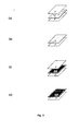
Fig. 2 illustrates teh examples of the construction of the security chip, -
Fig. 3 illustrates the examples of arrangements of the nanocomposite layers, -
Fig. 4 illustrates the principle of the intrinsic security chip, -
Fig. 5 illustrates the principle of the capacitive security chip, -
Fig. 6 illustrates examples of arrangements of layers of the nanocomposite material, -
Fig. 7 illustrates the examples of the shapes of the antenna, -
Fig. 8 illustrates the detection of the electroluminescent effect by a smartphone. - The security chip (1) is one of the layers of a polymer banknote. The security chip in the embodiment is an integral part of the hologram, i.e. is placed on the same layer of the film with a hologram.
- The chip begins to operate by applying an electromagnetic field generated using induced cell phone antenna (6). The security chip (1) is tuned in the frequency range of GSM 900 MHz to 2100 MHz.
- A smartphone or a phone working on GSM frequencies (6) is a control instrument inducing the security chip. The smartphone using dedicated application short-exciting the embedded antenna generates an electromagnetic field. Then bringing the smartphone nearer to the security chip (1), the signal reception by the graphene antenna occurs (2). The signal in the electromotive force processing chip (3) is converted to DC and then it powers the electroluminescent element (4), which starts to glow. The electroluminescent element (4) glows as long as the source is applied to the electromagnetic field of the security chip (1).
- Spontaneous manner of the security circuit operation is illustrated in
Figure 4 . - The application on a smartphone (6) also detects the chip operation (receiving glowing of the electroluminescent element) using a camera. In the event of activation of the chip - the application will notify the user with an additional message about the fact of the chip excitation.
- Detection of the electroluminescent effect by a smartphone is illustrated in Figure 9.
- Application functionality allows one to easily use it and also for a blind person to verify a banknote.
- The chip (1) is made so as to operate capacitively with the circuit closed with a finger (the "touch" option). The operation of the capacitive circuits is based on the phenomenon of the impact of the electric field with conductors, in particular the human body, which is filled with electrolytes and surrounded by a conductive layer of lossy dielectric - the skin. The electronic component that produces the electric field is a capacitor and as with any capacitor each part of the field goes out the covers. This field is called the boundary field. The system of covers in the touch switch is designed so that the field is the greatest and directed to the area available to the user's finger. The finger located in the boundary electric field introduces a certain capacity into the chip, which is called touch capacitance (CD).
- Capacitive mode of operation of the security chip is illustrated in
Figure 5 . - Depending on the design, the arrangement of graphene nanocomposite structure can take any form that can achieve maximum performance of the security chip during its use.
- The structure of the nanocomposite material security chip takes into account:
- using more layers of graphene in the material - the number of mononuclear layers depends on the conditions under which the security chip will operate.
- the use of graphene in the form of nanotubes, if the use of the properties of graphene, which is given by such construction are necessary to increase the effectiveness of the security chip.
- doping of graphene to modify some properties of the material, e.g.: optical, electrical, electromagnetic or mechanical.
- Examples of arrangement of conductive structures in nanocomposite are illustrated in
Figure 6 . - The components of the nanocomposite layer should be made in one of the selected ways:
- graphene layer (two-dimensional or structured, e.g. nanotubes) between two layers of polymer with a pin contact on the surface of one of the two polymer layers, where the security circuit will have the "touch" option of the capacitive circuit closing touching the contacts with a finger;
- graphene layer (two-dimensional or structured, e.g. nanotubes) immersed in the surface of a single polymer layer when the security chip is done without the "touch" option;
- doped graphene layer (two-dimensional or structured, e.g. nanotubes) between two layers of polymer with a pin contact on the surface of one of the two polymer layers, when the security circuit will have the "touch" option of the capacitive circuit closing touching the contacts with a finger;
- doped graphene layer (two-dimensional or structured, e.g. nanotubes) immersed in the surface of a single polymer layer when the security chip is done without the "touch" option;
- Examples of the nanocomposite layer chips are illustrated in
Figure 3 . - Other examples of the use of the security chip are authentication of pre-numbered documents, such as:
- a passport-the chip is an integral part of the cover;
- payment cards - the top layer of the card;
- other documents in the form of a payment card, such as a driving license, ID card;
- excise bands and prints;
- personal identifiers;
- license forms, certificates, etc.;
- label for products with high value and at risk of counterfeiting;
Claims (13)
- Security chip (1) against counterfeiting, in particular banknotes, characterized in that it comprises electronic circuit disposed on an elastic layer of nanocomposite graphene material comprising an antenna (2), an electroluminescent element (4) and preferably also an electromotive force processing chip (3) adapted to process the signal received by the DC powered security chip (1) powering the electroluminescent element (4), wherein the elastic layer graphene nanocomposite material comprises at least one layer of graphene (G) arranged on an adhesive layer, preferably polymer (P).
- The chip of claim 1, characterized in that it comprises a capacitive touch switch (5) configured to close the circuit chip (1) by a finger touching the contacts.
- The chip of claim 2, characterized in that the switch contacts (5) are led to the surface of at least one layer of adhesive.
- The chip of claim 1, 2 or 3, characterized in that at least one component of the security chip (1), and preferably each component of the chip, is made of graphene, and is an integral part of the flexible layer of graphene nanocomposite material.
- The chip according to any one of claims 1 to 4, characterized in that it is adapted to excitation by the GSM signal in the frequency range from 900 MHz to 2100 MHz.
- The chip according to any one of claims 1 to 5, characterized in that the graphene (G) is in a pure or doped (DP) form.
- The chip according to any one of claims 1 to 5, characterized in that it comprises a layer of graphene, and two adhesive layers, wherein the graphene layer (G) is located directly between the two layers of adhesive.
- The chip according to any one of claims 1 to 7, characterized in that graphene (G) is in a two-dimensional form having a thickness of one atom or more than one atom or three dimensional and preferably they are nanotubes arranged in different directions, in particular parallel or perpendicular to the surface of the adhesive.
- Use of the chip according to any one of claims from 1 to 8 for securing banknotes, holograms, documents, passports, credit cards, excise bands, excise forms, personal identifiers, certificates or product labels.
- The system for verifying the authenticity of documents, in particular banknotes, characterized in that it comprises a security chip (1) according to any one of claims 1 to 8 and a device (6) adapted for generating a signal exciting the chip(1).
- The system of claim 10, characterized in that the device (6) is adapted to record the signal generated by the electroluminescent element (4).
- The system of claim 10 or 11, characterized in that the device (6) is a mobile phone.
- The method of verifying the authenticity of documents, in particular banknotes, characterized in that the system of claim 10 or 11 or 12 is used.
Priority Applications (2)
| Application Number | Priority Date | Filing Date | Title |
|---|---|---|---|
| US14/571,201 US9378506B1 (en) | 2014-12-10 | 2014-12-15 | Security chip |
| EP14460115.0A EP3034314A1 (en) | 2014-12-18 | 2014-12-18 | Security chip against counterfeiting, especially banknotes |
Applications Claiming Priority (1)
| Application Number | Priority Date | Filing Date | Title |
|---|---|---|---|
| EP14460115.0A EP3034314A1 (en) | 2014-12-18 | 2014-12-18 | Security chip against counterfeiting, especially banknotes |
Publications (1)
| Publication Number | Publication Date |
|---|---|
| EP3034314A1 true EP3034314A1 (en) | 2016-06-22 |
Family
ID=52391773
Family Applications (1)
| Application Number | Title | Priority Date | Filing Date |
|---|---|---|---|
| EP14460115.0A Withdrawn EP3034314A1 (en) | 2014-12-10 | 2014-12-18 | Security chip against counterfeiting, especially banknotes |
Country Status (2)
| Country | Link |
|---|---|
| US (1) | US9378506B1 (en) |
| EP (1) | EP3034314A1 (en) |
Families Citing this family (1)
| Publication number | Priority date | Publication date | Assignee | Title |
|---|---|---|---|---|
| USD977988S1 (en) * | 2022-08-18 | 2023-02-14 | Weibo Wang | Tent water bag |
Citations (6)
| Publication number | Priority date | Publication date | Assignee | Title |
|---|---|---|---|---|
| US20090230197A1 (en) * | 2008-03-14 | 2009-09-17 | Colin Tanner | Method and apparatus for a contactless smartcard incorporating a mechanical switch |
| US20120217480A1 (en) | 2008-12-30 | 2012-08-30 | Hitachi Global Storage Technologies Netherlands B.V. | Method for manufacturing graphene electronics |
| US20130004658A1 (en) | 2011-06-30 | 2013-01-03 | Chung-Yen Yang | Method of forming antenna by utilizing graphene |
| FR2979852A1 (en) * | 2011-09-14 | 2013-03-15 | Arjowiggins Security | MULTILAYER STRUCTURE INTEGRATING AT LEAST ONE SAFETY ELEMENT |
| WO2013114116A1 (en) * | 2012-01-31 | 2013-08-08 | The University Of Manchester | Graphene composites |
| CN104217931A (en) * | 2013-05-29 | 2014-12-17 | 国家纳米科学中心 | Graphene doping method and doped graphene |
Family Cites Families (2)
| Publication number | Priority date | Publication date | Assignee | Title |
|---|---|---|---|---|
| DE102012203251B8 (en) * | 2012-03-01 | 2013-11-07 | Bundesdruckerei Gmbh | Contactless data transmission device, this containing security or value document |
| US9059188B1 (en) * | 2014-05-01 | 2015-06-16 | International Business Machines Corporation | Graphene resistor based tamper resistant identifier with contactless reading |
-
2014
- 2014-12-15 US US14/571,201 patent/US9378506B1/en not_active Expired - Fee Related
- 2014-12-18 EP EP14460115.0A patent/EP3034314A1/en not_active Withdrawn
Patent Citations (6)
| Publication number | Priority date | Publication date | Assignee | Title |
|---|---|---|---|---|
| US20090230197A1 (en) * | 2008-03-14 | 2009-09-17 | Colin Tanner | Method and apparatus for a contactless smartcard incorporating a mechanical switch |
| US20120217480A1 (en) | 2008-12-30 | 2012-08-30 | Hitachi Global Storage Technologies Netherlands B.V. | Method for manufacturing graphene electronics |
| US20130004658A1 (en) | 2011-06-30 | 2013-01-03 | Chung-Yen Yang | Method of forming antenna by utilizing graphene |
| FR2979852A1 (en) * | 2011-09-14 | 2013-03-15 | Arjowiggins Security | MULTILAYER STRUCTURE INTEGRATING AT LEAST ONE SAFETY ELEMENT |
| WO2013114116A1 (en) * | 2012-01-31 | 2013-08-08 | The University Of Manchester | Graphene composites |
| CN104217931A (en) * | 2013-05-29 | 2014-12-17 | 国家纳米科学中心 | Graphene doping method and doped graphene |
Also Published As
| Publication number | Publication date |
|---|---|
| US20160180350A1 (en) | 2016-06-23 |
| US9378506B1 (en) | 2016-06-28 |
Similar Documents
| Publication | Publication Date | Title |
|---|---|---|
| CN107438851B (en) | Mobile portable device for authenticating a security article and method of operating a portable authentication device | |
| EP2471027B1 (en) | A document with an integrated display and method of manufacture the same | |
| CN111095299B (en) | Information carrier, and methods of encoding and reading the information carrier | |
| EP2867825B1 (en) | Method and system for identifying a security document | |
| CN101960495B (en) | Valuable document with protection against forgery by way of thermochromic indicator | |
| WO2003054808A2 (en) | Devices and methods for the production of sheet material | |
| US20150199039A1 (en) | Input means for a touchscreen | |
| MX2009000071A (en) | Security or valuable document with at least two display mechanisms. | |
| CN101501710A (en) | Secure document, in particular electronic passport with enhanced security | |
| WO2010097342A3 (en) | Money purse or wallet for accommodating credit cards | |
| EA025462B1 (en) | A NON-CONTACT DATA TRANSFER DEVICE, CONTAINING ITS PROTECTED FROM A FAKE AND / OR A VALUABLE DOCUMENT AND A WAY TO MANUFACTURE A CONTACT-FREE DATA TRANSFER | |
| CN107657304B (en) | Electronic identity document | |
| CN102117515A (en) | A wireless fingerprint card | |
| CN103827892A (en) | Anti-scanner device for RFID cards | |
| CN209625254U (en) | Near-field communication equipment | |
| RU2315355C2 (en) | Forgery-protected document (variants) | |
| US9378506B1 (en) | Security chip | |
| CN206312196U (en) | chip card with fingerprint identification function | |
| JP5929513B2 (en) | Metal embedded RFID tag and data reader | |
| PL1673231T5 (en) | Security document provided with different marking characteristics | |
| EP1884887A1 (en) | Security document | |
| CN105051797B (en) | Device and method for checking the authenticity of value documents or security documents | |
| US9691013B2 (en) | Electronic circuit of a microprocessor proximity document and a proximity document | |
| CN203041012U (en) | Safety protection cutting sleeve of RFID (radio frequency identification device) | |
| US20170032235A1 (en) | Scanner resistant device with built in reading lens and led light |
Legal Events
| Date | Code | Title | Description |
|---|---|---|---|
| PUAI | Public reference made under article 153(3) epc to a published international application that has entered the european phase |
Free format text: ORIGINAL CODE: 0009012 |
|
| 17P | Request for examination filed |
Effective date: 20141218 |
|
| AK | Designated contracting states |
Kind code of ref document: A1 Designated state(s): AL AT BE BG CH CY CZ DE DK EE ES FI FR GB GR HR HU IE IS IT LI LT LU LV MC MK MT NL NO PL PT RO RS SE SI SK SM TR |
|
| AX | Request for extension of the european patent |
Extension state: BA ME |
|
| RAP1 | Party data changed (applicant data changed or rights of an application transferred) |
Owner name: RYBKA, WOJCIECH |
|
| RIN1 | Information on inventor provided before grant (corrected) |
Inventor name: RYBKA, WOJCIECH |
|
| RIN1 | Information on inventor provided before grant (corrected) |
Inventor name: NAWROCKI, PIOTR |
|
| 17Q | First examination report despatched |
Effective date: 20200326 |
|
| STAA | Information on the status of an ep patent application or granted ep patent |
Free format text: STATUS: THE APPLICATION IS DEEMED TO BE WITHDRAWN |
|
| 18D | Application deemed to be withdrawn |
Effective date: 20200806 |