EP3032582A2 - Structure and formation method of chip package structure - Google Patents
Structure and formation method of chip package structure Download PDFInfo
- Publication number
- EP3032582A2 EP3032582A2 EP15176380.2A EP15176380A EP3032582A2 EP 3032582 A2 EP3032582 A2 EP 3032582A2 EP 15176380 A EP15176380 A EP 15176380A EP 3032582 A2 EP3032582 A2 EP 3032582A2
- Authority
- EP
- European Patent Office
- Prior art keywords
- package
- interposer substrate
- conductive
- semiconductor die
- chip package
- Prior art date
- Legal status (The legal status is an assumption and is not a legal conclusion. Google has not performed a legal analysis and makes no representation as to the accuracy of the status listed.)
- Ceased
Links
Images



Classifications
-
- H—ELECTRICITY
- H10—SEMICONDUCTOR DEVICES; ELECTRIC SOLID-STATE DEVICES NOT OTHERWISE PROVIDED FOR
- H10W—GENERIC PACKAGES, INTERCONNECTIONS, CONNECTORS OR OTHER CONSTRUCTIONAL DETAILS OF DEVICES COVERED BY CLASS H10
- H10W20/00—Interconnections in chips, wafers or substrates
- H10W20/40—Interconnections external to wafers or substrates, e.g. back-end-of-line [BEOL] metallisations or vias connecting to gate electrodes
- H10W20/41—Interconnections external to wafers or substrates, e.g. back-end-of-line [BEOL] metallisations or vias connecting to gate electrodes characterised by their conductive parts
- H10W20/43—Layouts of interconnections
-
- H—ELECTRICITY
- H10—SEMICONDUCTOR DEVICES; ELECTRIC SOLID-STATE DEVICES NOT OTHERWISE PROVIDED FOR
- H10W—GENERIC PACKAGES, INTERCONNECTIONS, CONNECTORS OR OTHER CONSTRUCTIONAL DETAILS OF DEVICES COVERED BY CLASS H10
- H10W70/00—Package substrates; Interposers; Redistribution layers [RDL]
- H10W70/01—Manufacture or treatment
- H10W70/05—Manufacture or treatment of insulating or insulated package substrates, or of interposers, or of redistribution layers
- H10W70/08—Manufacture or treatment of insulating or insulated package substrates, or of interposers, or of redistribution layers by depositing layers on the chip or wafer, e.g. "chip-first" RDLs
- H10W70/09—Manufacture or treatment of insulating or insulated package substrates, or of interposers, or of redistribution layers by depositing layers on the chip or wafer, e.g. "chip-first" RDLs extending onto an encapsulation that laterally surrounds the chip or wafer, e.g. fan-out wafer level package [FOWLP] RDLs
-
- H—ELECTRICITY
- H10—SEMICONDUCTOR DEVICES; ELECTRIC SOLID-STATE DEVICES NOT OTHERWISE PROVIDED FOR
- H10W—GENERIC PACKAGES, INTERCONNECTIONS, CONNECTORS OR OTHER CONSTRUCTIONAL DETAILS OF DEVICES COVERED BY CLASS H10
- H10W70/00—Package substrates; Interposers; Redistribution layers [RDL]
- H10W70/60—Insulating or insulated package substrates; Interposers; Redistribution layers
- H10W70/611—Insulating or insulated package substrates; Interposers; Redistribution layers for connecting multiple chips together
- H10W70/614—Insulating or insulated package substrates; Interposers; Redistribution layers for connecting multiple chips together the multiple chips being integrally enclosed
-
- H—ELECTRICITY
- H10—SEMICONDUCTOR DEVICES; ELECTRIC SOLID-STATE DEVICES NOT OTHERWISE PROVIDED FOR
- H10W—GENERIC PACKAGES, INTERCONNECTIONS, CONNECTORS OR OTHER CONSTRUCTIONAL DETAILS OF DEVICES COVERED BY CLASS H10
- H10W70/00—Package substrates; Interposers; Redistribution layers [RDL]
- H10W70/60—Insulating or insulated package substrates; Interposers; Redistribution layers
- H10W70/62—Insulating or insulated package substrates; Interposers; Redistribution layers characterised by their interconnections
- H10W70/63—Vias, e.g. via plugs
- H10W70/635—Through-vias
-
- H—ELECTRICITY
- H10—SEMICONDUCTOR DEVICES; ELECTRIC SOLID-STATE DEVICES NOT OTHERWISE PROVIDED FOR
- H10W—GENERIC PACKAGES, INTERCONNECTIONS, CONNECTORS OR OTHER CONSTRUCTIONAL DETAILS OF DEVICES COVERED BY CLASS H10
- H10W72/00—Interconnections or connectors in packages
- H10W72/01—Manufacture or treatment
- H10W72/0198—Manufacture or treatment batch processes
-
- H—ELECTRICITY
- H10—SEMICONDUCTOR DEVICES; ELECTRIC SOLID-STATE DEVICES NOT OTHERWISE PROVIDED FOR
- H10W—GENERIC PACKAGES, INTERCONNECTIONS, CONNECTORS OR OTHER CONSTRUCTIONAL DETAILS OF DEVICES COVERED BY CLASS H10
- H10W74/00—Encapsulations, e.g. protective coatings
- H10W74/10—Encapsulations, e.g. protective coatings characterised by their shape or disposition
- H10W74/111—Encapsulations, e.g. protective coatings characterised by their shape or disposition the semiconductor body being completely enclosed
- H10W74/121—Encapsulations, e.g. protective coatings characterised by their shape or disposition the semiconductor body being completely enclosed by multiple encapsulations, e.g. by a thin protective coating and a thick encapsulation
-
- H—ELECTRICITY
- H10—SEMICONDUCTOR DEVICES; ELECTRIC SOLID-STATE DEVICES NOT OTHERWISE PROVIDED FOR
- H10W—GENERIC PACKAGES, INTERCONNECTIONS, CONNECTORS OR OTHER CONSTRUCTIONAL DETAILS OF DEVICES COVERED BY CLASS H10
- H10W74/00—Encapsulations, e.g. protective coatings
- H10W74/10—Encapsulations, e.g. protective coatings characterised by their shape or disposition
- H10W74/111—Encapsulations, e.g. protective coatings characterised by their shape or disposition the semiconductor body being completely enclosed
- H10W74/129—Encapsulations, e.g. protective coatings characterised by their shape or disposition the semiconductor body being completely enclosed forming a chip-scale package [CSP]
-
- H—ELECTRICITY
- H10—SEMICONDUCTOR DEVICES; ELECTRIC SOLID-STATE DEVICES NOT OTHERWISE PROVIDED FOR
- H10W—GENERIC PACKAGES, INTERCONNECTIONS, CONNECTORS OR OTHER CONSTRUCTIONAL DETAILS OF DEVICES COVERED BY CLASS H10
- H10W90/00—Package configurations
-
- H—ELECTRICITY
- H10—SEMICONDUCTOR DEVICES; ELECTRIC SOLID-STATE DEVICES NOT OTHERWISE PROVIDED FOR
- H10W—GENERIC PACKAGES, INTERCONNECTIONS, CONNECTORS OR OTHER CONSTRUCTIONAL DETAILS OF DEVICES COVERED BY CLASS H10
- H10W70/00—Package substrates; Interposers; Redistribution layers [RDL]
- H10W70/60—Insulating or insulated package substrates; Interposers; Redistribution layers
-
- H—ELECTRICITY
- H10—SEMICONDUCTOR DEVICES; ELECTRIC SOLID-STATE DEVICES NOT OTHERWISE PROVIDED FOR
- H10W—GENERIC PACKAGES, INTERCONNECTIONS, CONNECTORS OR OTHER CONSTRUCTIONAL DETAILS OF DEVICES COVERED BY CLASS H10
- H10W72/00—Interconnections or connectors in packages
- H10W72/20—Bump connectors, e.g. solder bumps or copper pillars; Dummy bumps; Thermal bumps
- H10W72/241—Dispositions, e.g. layouts
-
- H—ELECTRICITY
- H10—SEMICONDUCTOR DEVICES; ELECTRIC SOLID-STATE DEVICES NOT OTHERWISE PROVIDED FOR
- H10W—GENERIC PACKAGES, INTERCONNECTIONS, CONNECTORS OR OTHER CONSTRUCTIONAL DETAILS OF DEVICES COVERED BY CLASS H10
- H10W90/00—Package configurations
- H10W90/701—Package configurations characterised by the relative positions of pads or connectors relative to package parts
- H10W90/721—Package configurations characterised by the relative positions of pads or connectors relative to package parts of bump connectors
- H10W90/722—Package configurations characterised by the relative positions of pads or connectors relative to package parts of bump connectors between stacked chips
Definitions
- the disclosure relates to structures and formation methods of chip package structures, and in particular to structures and formation methods of chip package structures including multiple semiconductor dies.
- a chip package structure not only provides chips with protection from environmental contaminants, but it also provides a connection interface for the chips packaged therein.
- manufacturers and others in the electronics industry continually seek ways to reduce the size of integrated circuits used in electronic products. In that regard, three-dimensional type integrated circuit packaging techniques have been developed and put into practice.
- PoP package-on-package
- a PoP device may combine vertically, for example, discrete memory and logic packages.
- a chip package structure includes a first package which includes at least a semiconductor die, a dielectric structure surrounding the semiconductor die, and a plurality of conductive structures penetrating through the dielectric structure and surrounding the semiconductor die.
- the package structure also includes an interposer substrate over the first package and a plurality of conductive features in or over the interposer substrate.
- the package structure further includes a second package over the interposer substrate, and the first package electrically couples the second package through the conductive structures and the conductive features.
- a method for forming a package structure includes providing a first package.
- the first package includes at least a semiconductor die, a dielectric structure surrounding the semiconductor die, and a plurality of conductive structures penetrating through the dielectric structure and surrounding the semiconductor die.
- the method also includes bonding an interposer substrate over the first package.
- the method further includes bonding a second package over the interposer substrate.
- first and second features are formed in direct contact
- additional features may be formed between the first and second features, such that the first and second features may not be in direct contact
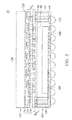
- Fig. 1 is a cross-sectional view of a package structure 10, in accordance with some embodiments.
- a package 102 is provided.
- the package 102 includes at least one semiconductor die, such as a semiconductor die 103.
- the package 102 also includes a dielectric structure 104 which surrounds the semiconductor die 103.
- the package 102 further includes one or more conductive structures 106 which penetrate through the dielectric structure 104 and surround the semiconductor die 103.
- the dielectric structure 104 is partially removed to form through holes. Afterwards, the through holes are filled with one or more conductive materials to form the conductive structures 106.
- the through holes are formed using a laser drilling process, photolithography and etching processes, other applicable processes, or a combination thereof.
- the semiconductor die 103 includes one or more logic devices.
- the dielectric structure 104 includes a molding compound material.
- the conductive structures 106 are made of copper, aluminum, tungsten, nickel, titanium, gold, platinum, other suitable conductive materials, or a combination thereof.
- the package 102 includes a dielectric layer 108 and redistribution layers 110 under the dielectric structure 104, the conductive structures 106, and the semiconductor die 103, in accordance with some embodiments.
- the redistribution layers form electrical connections to the conductive structures 106 and the pads (not shown) of the semiconductor die 103. Therefore, electrical paths to the semiconductor die 103 are fanned out and led to opposite sides of the semiconductor die 103.
- multiple deposition and patterning processes are used to form the dielectric layer 108 and the redistribution layers 110.
- the dielectric layer 108 includes multiple stacked layers.
- the dielectric layer 108 is made of polyimide, silicon oxide, silicon nitride, epoxy-based materials, other suitable dielectric materials, or a combination thereof.
- the redistribution layers 110 include multiple conductive lines and conductive vias.
- the redistribution layers 110 are made of copper, aluminum, platinum, tungsten, titanium, platinum, nickel, gold, other suitable conductive materials, or a combination thereof.
- a number of conductive elements 112 are formed under the redistribution layers 110 and the dielectric layer 108, in accordance with some embodiments.
- Each of the conductive elements 112 is electrically connected to at least one of the redistribution layers 110.
- the conductive elements 112 are made of a solder material.
- the conductive elements 112 include metal posts or metal pillars.
- the conductive elements 112 include copper posts and/or copper pillars.
- the conductive elements 112 are formed using a solder ball placement process, a plating process, other applicable processes, or a combination thereof.
- the package 102 may be formed using a variety of methods.
- the package 102 is formed using a wafer-level packaging process.
- a plurality of semiconductor dies are placed over a carrier substrate such as a glass wafer, a semiconductor wafer, or the like.
- a wafer molding material is applied over the semiconductor dies and the carrier substrate to fix the semiconductor dies.
- the dielectric layer 108 and the redistribution layers 110 are formed over the semiconductor dies.
- the redistribution layers 110 are electrically and correspondingly connected to the semiconductor dies.
- the conductive elements 112 are then formed over the redistribution layers 110.
- the carrier substrate is removed, and another carrier is attached to the conductive elements 112.
- Another wafer molding material may be applied over the semiconductor dies to form the dielectric structure 104.
- the conductive structures 106 are then formed in the dielectric structure 104.
- a dicing process is performed to form a plurality of packages 102. Alternatively, the dicing process is not performed at this stage. It should be appreciated, however, that embodiments of the disclosure are not limited thereto. In some other embodiments, the wafer-level packaging process is performed in a different way.
- an interposer substrate 114 is bonded over the package 102, in accordance with some embodiments.
- the interposer substrate 114 is not in direct contact with the package 102.
- the interposer substrate 114 is separated from the package 102.
- the interposer substrate 114 is separated from an upper surface of the package 102 by a distance D 1 .
- the distance D 1 may be in a range from about 10 ⁇ m to about 40 ⁇ m. In some other embodiments, the distance D 1 is in a range from about 15 ⁇ m to about 30 ⁇ m.
- the interposer substrate 114 is made of a dielectric material.
- the dielectric material may include epoxy, cyanate ester, polyimide, polytetrafluoroethylene, allylated polyphenylene ether, other suitable dielectric materials, or a combination thereof.
- the interposed substrate 114 includes fibers dispersed in the dielectric material. For example, glass fibers are added into the dielectric material.
- the interposer substrate 114 is bonded over the package 102 by a plurality of conductive elements 116 between the interposer substrate 114 and the package 102, in accordance with some embodiments.
- each of the conductive elements 116 is electrically connected to at least one of the conductive structures 106.
- the conductive elements 116 are made of one or more solder materials, other suitable conductive materials, or a combination thereof.
- the conductive elements 116 are formed using a solder ball placement process, a plating process, other applicable processes, or a combination thereof.
- a reflow process is performed to bond the interposer substrate 114 with the package 102 through the conductive elements 116.
- a plurality of conductive features 118 are formed in and/or over the interposer substrate 114, in accordance with some embodiments.
- the conductive features 118 provide electrical connections for elements disposed over opposite sides of the interposer substrate 114.
- the conductive features 118 are made of cooper, aluminum, tungsten, titanium, gold, platinum, nickel, other suitable conductive materials, or a combination thereof.
- the interposer substrate 114 and the conductive features 114 together form a circuit board.
- the interposer substrate 114 and the conductive features 114 are formed using a process suitable for forming a printed circuit board.
- different materials and/or processes are used to form the interposer substrate 114 and the conductive features 114.
- a package 122 is provided and bonded over the interposer substrate 114, in accordance with some embodiments.
- the package 122 includes a semiconductor die 124.
- the semiconductor die 124 includes one or more memory devices.
- the semiconductor die 124 includes one or more logic devices.
- a dielectric layer 126 and multiple redistribution layers 128 are formed over the semiconductor die 124, as shown in Fig. 1 in accordance with some embodiments.
- the dielectric layer 126 includes multiple stacked layers.
- the dielectric layer 126 is made of polyimide, silicon oxide, silicon nitride, epoxy-based materials, other suitable dielectric materials, or a combination thereof.
- the redistribution layers 128 include multiple conductive lines and conductive vias. In some embodiments, the redistribution layers 128 are made of copper, aluminum, platinum, tungsten, titanium, platinum, nickel, gold, other suitable conductive materials, or a combination thereof.
- the package 122 is not limited to being bonded over the interposer substrate 114 after the interposed substrate 114 is bonded over the package 102. In some other embodiments, the package 122 is bonded over the interposed substrate 114. Afterwards, the interposed substrate 114 is bonded over the package 102.
- the interposer substrate 114 is not in direct contact with the package 122. In some embodiments, the interposer substrate 114 is separated from the package 122. For example, the interposer substrate 114 is separated from a lower surface of the package 122 by a distance D 2 .
- the distance D 2 may be in a range from about 10 ⁇ m to about 50 ⁇ m. In some other embodiments, the distance D 2 is in a range from about 15 ⁇ m to about 40 ⁇ m. In some embodiments, the distance D 2 is longer than the distance D 1 .
- the package 122 is bonded over the interposer substrate 114 by a plurality of conductive elements 120 between the interposer substrate 114 and the package 122, in accordance with some embodiments.
- each of the conductive elements 120 is electrically connected to at least one of the conductive features 118.
- each of the conductive elements 120 is electrically connected to at least one of the conductive structures 106 penetrating through the dielectric structure 104.
- the conductive elements 120 are electrically connected to the conductive structures 106 through the conductive features 118.
- the conductive elements 120 are made of one or more solder materials, other suitable conductive materials, or a combination thereof.
- the conductive elements 120 are formed using a solder ball placement process, a plating process, other applicable processes, or a combination thereof. In some embodiments, a reflow process is performed to bond the package 122 with the interposer substrate 114 through the conductive elements 120.
- Embodiments of the disclosure use the interposer substrate 114 to build electrical connections between the packages 102 and 122 over opposite sides of the interposer substrate 114.
- the bonding between the interposer substrate 114 and the package 102 and/or the package 122 might not be good enough and a rework process may need to be performed.
- the interposer substrate 114 is not in direct contact with both of the packages 102 and 122, the rework process could be performed more easily. Damages to the packages 102 and 122 may be prevented or significantly reduced during the rework process.
- the interposer substrate 114 provides stronger mechanical support. As a result, the processes, such as the bonding processes, may be performed in a more reliable way.
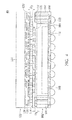
- Fig. 2 is a cross-sectional view of a package structure 20, in accordance with some embodiments.
- the package structure 20 is similar to the package structure 10 shown in Fig. 1 .
- a package 102' similar to the package 102 is provided.
- the package 102' includes a dielectric structure 105 and a dielectric structure 104'.
- the dielectric structure 105 surrounds the semiconductor die 103
- the dielectric structure 104' surrounds the dielectric structure 105 and the semiconductor die 103.
- materials of the dielectric structures 104' and 105 are different from each other.
- the dielectric structure 105 is made of a molding compound material.
- the dielectric structure 104' is made of a material similar to that of a printed circuit board.
- a printed circuit board is partially removed to form a recess where the semiconductor die 103 is then positioned. Afterwards, a molding compound material is applied into the recess to form the dielectric structure 105 which surrounds and covers the semiconductor die 103.
- the conductive structures 106 are formed in the dielectric structure 104', in accordance with some embodiments. Similarly, the conductive structures 106 in the dielectric structure 106 are used as conductive bridges between the packages 102' and 122.
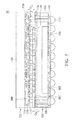
- Fig. 3 is a cross-sectional view of a package structure 30, in accordance with some embodiments.
- the package structure 30 is similar to the package structure 10 shown in Fig. 1 .
- conductive elements 116' and 120' are used to bond the interposer substrate 114 with the packages 102 and 122, respectively.
- the conductive elements 116' include metal pillars.
- the metal pillars are copper pillars.
- the conductive elements 116' are made of a metal material different from copper.
- the metal pillars are bonded to the conductive structures 106 through a bonding material.
- the bonding material includes a solder material.
- the metal pillars are bonded to the conductive features 118 through a bonding material, such as a solder material.
- the conductive elements 120' include metal pillars.
- the metal pillars are copper pillars.
- the conductive elements 120' are made of a metal material different from copper.
- the metal pillars are bonded to the redistribution layers 128 through a bonding material.
- the bonding material includes a solder material.
- each of the conductive elements 120' is larger than each of the conductive elements 116'.
- Fig. 4 is a cross-sectional view of a package structure 40, in accordance with some embodiments.
- the package structure 40 is similar to the package structure 20 shown in Fig. 2 .
- the conductive elements 116' and 120' are used to bond the interposer substrate 114 with the packages 102 and 122, as shown in Fig. 4 in accordance with some embodiments.
- Fig. 5 is a cross-sectional view of a package structure 50, in accordance with some embodiments.
- the package structure 50 is similar to the package structure 10 shown in Fig. 1 .
- an underfill material 502 is formed between the interposer substrate 114 and the package 102, in accordance with some embodiments.
- an underfill material 504 is formed between the interposer substrate 114 and the package 122, in accordance with some embodiments.
- the under fill materials 502 and 504 protect the conductive elements 116 and 120, respectively.
- the under fill materials 502 and 504 are used to protect the conductive elements 116' and 120' shown in Fig. 3 .
- Fig. 6 is a cross-sectional view of a package structure 60, in accordance with some embodiments.
- the package structure 60 is similar to the package structure 20 shown in Fig. 2 .
- an underfill material 502 is formed between the interposer substrate 114 and the package 102', in accordance with some embodiments.
- an underfill material 504 is formed between the interposer substrate 114 and the package 122, in accordance with some embodiments.
- the under fill materials 502 and 504 protect the conductive elements 116 and 120, respectively. In some embodiments, the under fill materials 502 and 504 are used to protect the conductive elements 116' and 120' shown in Fig. 4 .
- Embodiments of the disclosure use an interposer substrate to bond two or more packages together.
- the interposer substrate builds electrical connections between the packages over opposite sides of the interposer substrate.
- the interposer substrate provides larger process windows and stronger support to the packages. For example, a rework process, if needed, can be performed more easily. As a result, the associated processing cost and processing time are reduced significantly.
Landscapes
- Production Of Multi-Layered Print Wiring Board (AREA)
- Engineering & Computer Science (AREA)
- Structures Or Materials For Encapsulating Or Coating Semiconductor Devices Or Solid State Devices (AREA)
- Internal Circuitry In Semiconductor Integrated Circuit Devices (AREA)
- Microelectronics & Electronic Packaging (AREA)
- Physics & Mathematics (AREA)
- Geometry (AREA)
- Manufacturing & Machinery (AREA)
Abstract
Description
- The disclosure relates to structures and formation methods of chip package structures, and in particular to structures and formation methods of chip package structures including multiple semiconductor dies.
- A chip package structure not only provides chips with protection from environmental contaminants, but it also provides a connection interface for the chips packaged therein. As the demand for smaller electronic products grows, manufacturers and others in the electronics industry continually seek ways to reduce the size of integrated circuits used in electronic products. In that regard, three-dimensional type integrated circuit packaging techniques have been developed and put into practice.
- Stacked packaging schemes, such as package-on-package (PoP) packaging, have become increasingly popular. As the name implies, PoP is a semiconductor packaging innovation that involves stacking one package on top of another package. A PoP device may combine vertically, for example, discrete memory and logic packages.
- New packaging technologies have been developed to improve the density and functions of semiconductor devices. These relatively new types of packaging technologies for semiconductor devices face manufacturing challenges.
- In accordance with some embodiments, a chip package structure is provided. The chip package structure includes a first package which includes at least a semiconductor die, a dielectric structure surrounding the semiconductor die, and a plurality of conductive structures penetrating through the dielectric structure and surrounding the semiconductor die. The package structure also includes an interposer substrate over the first package and a plurality of conductive features in or over the interposer substrate. The package structure further includes a second package over the interposer substrate, and the first package electrically couples the second package through the conductive structures and the conductive features.
- In accordance with some embodiments, a method for forming a package structure is provided. The method includes providing a first package. The first package includes at least a semiconductor die, a dielectric structure surrounding the semiconductor die, and a plurality of conductive structures penetrating through the dielectric structure and surrounding the semiconductor die. The method also includes bonding an interposer substrate over the first package. The method further includes bonding a second package over the interposer substrate.
- A detailed description is given in the following embodiments with reference to the accompanying drawings.
- The present disclosure can be more fully understood by reading the subsequent detailed description and examples with references made to the accompanying drawings.
-
Fig. 1 is a cross-sectional view of a package structure, in accordance with some embodiments. -
Fig. 2 is a cross-sectional view of a package structure, in accordance with some embodiments. -
Fig. 3 is a cross-sectional view of a package structure, in accordance with some embodiments. -
Fig. 4 is a cross-sectional view of a package structure, in accordance with some embodiments. -
Fig. 5 is a cross-sectional view of a package structure, in accordance with some embodiments. -
Fig. 6 is a cross-sectional view of a package structure, in accordance with some embodiments. - The making and using of the embodiments of the disclosure are discussed in detail below. It should be appreciated, however, that the embodiments can be embodied in a wide variety of specific contexts. The specific embodiments discussed are merely illustrative, and do not limit the scope of the disclosure.
- It should be understood that the following disclosure provides many different embodiments, or examples, for implementing different features of the disclosure. Specific examples of components and arrangements are described below to simplify the present disclosure. These are, of course, merely examples and are not intended to be limiting. Moreover, the performance of a first process before a second process in the description that follows may include embodiments in which the second process is performed immediately after the first process, and may also include embodiments in which additional processes may be performed between the first and second processes. Various features may be arbitrarily drawn in different scales for the sake of simplicity and clarity. Furthermore, the formation of a first feature over or on a second feature in the description that follows include embodiments in which the first and second features are formed in direct contact, and may also include embodiments in which additional features may be formed between the first and second features, such that the first and second features may not be in direct contact.
- Some variations of the embodiments are described. Throughout the various views and illustrative embodiments, like reference numbers are used to designate like elements.
-
Fig. 1 is a cross-sectional view of apackage structure 10, in accordance with some embodiments. Apackage 102 is provided. In some embodiments, thepackage 102 includes at least one semiconductor die, such as asemiconductor die 103. Thepackage 102 also includes adielectric structure 104 which surrounds the semiconductor die 103. Thepackage 102 further includes one or moreconductive structures 106 which penetrate through thedielectric structure 104 and surround the semiconductor die 103. In some embodiments, thedielectric structure 104 is partially removed to form through holes. Afterwards, the through holes are filled with one or more conductive materials to form theconductive structures 106. In some embodiments, the through holes are formed using a laser drilling process, photolithography and etching processes, other applicable processes, or a combination thereof. - In some embodiments, the semiconductor die 103 includes one or more logic devices. In some embodiments, the
dielectric structure 104 includes a molding compound material. In some embodiments, theconductive structures 106 are made of copper, aluminum, tungsten, nickel, titanium, gold, platinum, other suitable conductive materials, or a combination thereof. - As shown in
Fig. 1 , thepackage 102 includes adielectric layer 108 andredistribution layers 110 under thedielectric structure 104, theconductive structures 106, and the semiconductor die 103, in accordance with some embodiments. The redistribution layers form electrical connections to theconductive structures 106 and the pads (not shown) of thesemiconductor die 103. Therefore, electrical paths to thesemiconductor die 103 are fanned out and led to opposite sides of the semiconductor die 103. In some embodiments, multiple deposition and patterning processes are used to form thedielectric layer 108 and theredistribution layers 110. - In some embodiments, the
dielectric layer 108 includes multiple stacked layers. In some embodiments, thedielectric layer 108 is made of polyimide, silicon oxide, silicon nitride, epoxy-based materials, other suitable dielectric materials, or a combination thereof. In some embodiments, theredistribution layers 110 include multiple conductive lines and conductive vias. In some embodiments, theredistribution layers 110 are made of copper, aluminum, platinum, tungsten, titanium, platinum, nickel, gold, other suitable conductive materials, or a combination thereof. - As shown in
Fig. 1 , a number ofconductive elements 112 are formed under theredistribution layers 110 and thedielectric layer 108, in accordance with some embodiments. Each of theconductive elements 112 is electrically connected to at least one of theredistribution layers 110. In some embodiments, theconductive elements 112 are made of a solder material. In some other embodiments, theconductive elements 112 include metal posts or metal pillars. For example, theconductive elements 112 include copper posts and/or copper pillars. In some embodiments, theconductive elements 112 are formed using a solder ball placement process, a plating process, other applicable processes, or a combination thereof. - The
package 102 may be formed using a variety of methods. In some embodiments, thepackage 102 is formed using a wafer-level packaging process. In some embodiments, a plurality of semiconductor dies are placed over a carrier substrate such as a glass wafer, a semiconductor wafer, or the like. Afterwards, a wafer molding material is applied over the semiconductor dies and the carrier substrate to fix the semiconductor dies. Then, thedielectric layer 108 and the redistribution layers 110 are formed over the semiconductor dies. The redistribution layers 110 are electrically and correspondingly connected to the semiconductor dies. Theconductive elements 112 are then formed over the redistribution layers 110. Afterwards, the carrier substrate is removed, and another carrier is attached to theconductive elements 112. Another wafer molding material may be applied over the semiconductor dies to form thedielectric structure 104. Theconductive structures 106 are then formed in thedielectric structure 104. Afterwards, a dicing process is performed to form a plurality ofpackages 102. Alternatively, the dicing process is not performed at this stage. It should be appreciated, however, that embodiments of the disclosure are not limited thereto. In some other embodiments, the wafer-level packaging process is performed in a different way. - As shown in
Fig. 1 , aninterposer substrate 114 is bonded over thepackage 102, in accordance with some embodiments. In some embodiments, theinterposer substrate 114 is not in direct contact with thepackage 102. In some embodiments, theinterposer substrate 114 is separated from thepackage 102. For example, theinterposer substrate 114 is separated from an upper surface of thepackage 102 by a distance D1. The distance D1 may be in a range from about 10 µm to about 40 µm. In some other embodiments, the distance D1 is in a range from about 15 µm to about 30 µm. In some embodiments, theinterposer substrate 114 is made of a dielectric material. The dielectric material may include epoxy, cyanate ester, polyimide, polytetrafluoroethylene, allylated polyphenylene ether, other suitable dielectric materials, or a combination thereof. In some embodiments, the interposedsubstrate 114 includes fibers dispersed in the dielectric material. For example, glass fibers are added into the dielectric material. - As shown in
Fig. 1 , theinterposer substrate 114 is bonded over thepackage 102 by a plurality ofconductive elements 116 between theinterposer substrate 114 and thepackage 102, in accordance with some embodiments. In some embodiments, each of theconductive elements 116 is electrically connected to at least one of theconductive structures 106. In some embodiments, theconductive elements 116 are made of one or more solder materials, other suitable conductive materials, or a combination thereof. In some embodiments, theconductive elements 116 are formed using a solder ball placement process, a plating process, other applicable processes, or a combination thereof. In some embodiments, a reflow process is performed to bond theinterposer substrate 114 with thepackage 102 through theconductive elements 116. - As shown in
Fig. 1 , a plurality ofconductive features 118 are formed in and/or over theinterposer substrate 114, in accordance with some embodiments. The conductive features 118 provide electrical connections for elements disposed over opposite sides of theinterposer substrate 114. In some embodiments, theconductive features 118 are made of cooper, aluminum, tungsten, titanium, gold, platinum, nickel, other suitable conductive materials, or a combination thereof. In some embodiments, theinterposer substrate 114 and theconductive features 114 together form a circuit board. In some embodiments, theinterposer substrate 114 and theconductive features 114 are formed using a process suitable for forming a printed circuit board. However, it should be appreciated that embodiments of the disclosure are not limited thereto. In some other embodiments, different materials and/or processes are used to form theinterposer substrate 114 and the conductive features 114. - As shown in
Fig. 1 , apackage 122 is provided and bonded over theinterposer substrate 114, in accordance with some embodiments. In some embodiments, thepackage 122 includes asemiconductor die 124. In some embodiments, the semiconductor die 124 includes one or more memory devices. In some embodiments, the semiconductor die 124 includes one or more logic devices. Adielectric layer 126 andmultiple redistribution layers 128 are formed over the semiconductor die 124, as shown inFig. 1 in accordance with some embodiments. In some embodiments, thedielectric layer 126 includes multiple stacked layers. In some embodiments, thedielectric layer 126 is made of polyimide, silicon oxide, silicon nitride, epoxy-based materials, other suitable dielectric materials, or a combination thereof. In some embodiments, the redistribution layers 128 include multiple conductive lines and conductive vias. In some embodiments, the redistribution layers 128 are made of copper, aluminum, platinum, tungsten, titanium, platinum, nickel, gold, other suitable conductive materials, or a combination thereof. - Embodiments of the disclosure have many variations. For example, the
package 122 is not limited to being bonded over theinterposer substrate 114 after the interposedsubstrate 114 is bonded over thepackage 102. In some other embodiments, thepackage 122 is bonded over the interposedsubstrate 114. Afterwards, the interposedsubstrate 114 is bonded over thepackage 102. - In some embodiments, the
interposer substrate 114 is not in direct contact with thepackage 122. In some embodiments, theinterposer substrate 114 is separated from thepackage 122. For example, theinterposer substrate 114 is separated from a lower surface of thepackage 122 by a distance D2. The distance D2 may be in a range from about 10 µm to about 50 µm. In some other embodiments, the distance D2 is in a range from about 15 µm to about 40 µm. In some embodiments, the distance D2 is longer than the distance D1. - As shown in
Fig. 1 , thepackage 122 is bonded over theinterposer substrate 114 by a plurality ofconductive elements 120 between theinterposer substrate 114 and thepackage 122, in accordance with some embodiments. In some embodiments, each of theconductive elements 120 is electrically connected to at least one of the conductive features 118. In some embodiments, each of theconductive elements 120 is electrically connected to at least one of theconductive structures 106 penetrating through thedielectric structure 104. For example, theconductive elements 120 are electrically connected to theconductive structures 106 through the conductive features 118. In some embodiments, theconductive elements 120 are made of one or more solder materials, other suitable conductive materials, or a combination thereof. In some embodiments, theconductive elements 120 are formed using a solder ball placement process, a plating process, other applicable processes, or a combination thereof. In some embodiments, a reflow process is performed to bond thepackage 122 with theinterposer substrate 114 through theconductive elements 120. - Embodiments of the disclosure use the
interposer substrate 114 to build electrical connections between thepackages interposer substrate 114. In some cases, the bonding between theinterposer substrate 114 and thepackage 102 and/or thepackage 122 might not be good enough and a rework process may need to be performed. Because theinterposer substrate 114 is not in direct contact with both of thepackages packages interposer substrate 114 provides stronger mechanical support. As a result, the processes, such as the bonding processes, may be performed in a more reliable way. - Embodiments of the disclosure have many variations.
Fig. 2 is a cross-sectional view of apackage structure 20, in accordance with some embodiments. Thepackage structure 20 is similar to thepackage structure 10 shown inFig. 1 . Apackage 102' similar to thepackage 102 is provided. In some embodiments, thepackage 102' includes adielectric structure 105 and a dielectric structure 104'. As shown inFig. 2 , thedielectric structure 105 surrounds the semiconductor die 103, and the dielectric structure 104' surrounds thedielectric structure 105 and the semiconductor die 103. In some embodiments, materials of thedielectric structures 104' and 105 are different from each other. In some embodiments, thedielectric structure 105 is made of a molding compound material. In some embodiments, the dielectric structure 104' is made of a material similar to that of a printed circuit board. In some embodiments, a printed circuit board is partially removed to form a recess where the semiconductor die 103 is then positioned. Afterwards, a molding compound material is applied into the recess to form thedielectric structure 105 which surrounds and covers the semiconductor die 103. - As shown in
Fig. 2 , theconductive structures 106 are formed in the dielectric structure 104', in accordance with some embodiments. Similarly, theconductive structures 106 in thedielectric structure 106 are used as conductive bridges between thepackages - Embodiments of the disclosure have many variations.
Fig. 3 is a cross-sectional view of apackage structure 30, in accordance with some embodiments. Thepackage structure 30 is similar to thepackage structure 10 shown inFig. 1 . As shown inFig. 3 , conductive elements 116' and 120' are used to bond theinterposer substrate 114 with thepackages conductive structures 106 through a bonding material. For example, the bonding material includes a solder material. Similarly, the metal pillars are bonded to theconductive features 118 through a bonding material, such as a solder material. - In some embodiments, the conductive elements 120' include metal pillars. For example, the metal pillars are copper pillars. In some other embodiments, the conductive elements 120' are made of a metal material different from copper. In some embodiments, the metal pillars are bonded to the redistribution layers 128 through a bonding material. For example, the bonding material includes a solder material. In some embodiments, each of the conductive elements 120' is larger than each of the conductive elements 116'.
-
Fig. 4 is a cross-sectional view of apackage structure 40, in accordance with some embodiments. Thepackage structure 40 is similar to thepackage structure 20 shown inFig. 2 . Similar to the embodiments shown inFig. 3 , the conductive elements 116' and 120' are used to bond theinterposer substrate 114 with thepackages Fig. 4 in accordance with some embodiments. - Embodiments of the disclosure have many variations.
Fig. 5 is a cross-sectional view of apackage structure 50, in accordance with some embodiments. Thepackage structure 50 is similar to thepackage structure 10 shown inFig. 1 . As shown inFig. 5 , anunderfill material 502 is formed between theinterposer substrate 114 and thepackage 102, in accordance with some embodiments. As shown inFig. 5 , anunderfill material 504 is formed between theinterposer substrate 114 and thepackage 122, in accordance with some embodiments. The under fillmaterials conductive elements materials Fig. 3 . - Embodiments of the disclosure have many variations.
Fig. 6 is a cross-sectional view of apackage structure 60, in accordance with some embodiments. Thepackage structure 60 is similar to thepackage structure 20 shown inFig. 2 . As shown inFig. 6 , anunderfill material 502 is formed between theinterposer substrate 114 and thepackage 102', in accordance with some embodiments. As shown inFig. 5 , anunderfill material 504 is formed between theinterposer substrate 114 and thepackage 122, in accordance with some embodiments. The under fillmaterials conductive elements materials Fig. 4 . - Embodiments of the disclosure use an interposer substrate to bond two or more packages together. The interposer substrate builds electrical connections between the packages over opposite sides of the interposer substrate. The interposer substrate provides larger process windows and stronger support to the packages. For example, a rework process, if needed, can be performed more easily. As a result, the associated processing cost and processing time are reduced significantly.
- Although the embodiments and their advantages have been described in detail, it should be understood that various changes, substitutions, and alterations can be made herein without departing from the spirit and scope of the embodiments as defined by the appended claims. Moreover, the scope of the present application is not intended to be limited to the particular embodiments of the process, machine, manufacture, composition of matter, means, methods, and steps described in the specification. As one of ordinary skill in the art will readily appreciate from the disclosure, processes, machines, manufacture, compositions of matter, means, methods, or steps, presently existing or later to be developed, that perform substantially the same function or achieve substantially the same result as the corresponding embodiments described herein may be utilized according to the disclosure. Accordingly, the appended claims are intended to include within their scope such processes, machines, manufacture, compositions of matter, means, methods, or steps. In addition, each claim constitutes a separate embodiment, and the combination of various claims and embodiments are within the scope of the disclosure.
Claims (15)
- A chip package structure, comprising:a first package, wherein the first package comprises:at least a semiconductor die;a dielectric structure surrounding the semiconductor die; anda plurality of conductive structures penetrating through the dielectric structure and surrounding the semiconductor die;an interposer substrate over the first package;a plurality of conductive features in or over the interposer substrate; anda second package over the interposer substrate, wherein the first package electrically couples the second package through the conductive structures and the conductive features.
- The chip package structure as claimed in claim 1, wherein the interposer substrate is separated from the first package.
- The chip package structure as claimed in claim 1 or 2, further comprising a plurality of conductive elements between the interposer substrate and the first package, wherein each of the conductive elements is electrically connected to at least one of the conductive structures.
- The chip package structure as claimed in claim 3, wherein the conductive elements comprise a solder material.
- The chip package structure as claimed in claim 3 or 4, wherein the conductive elements comprise copper pillars.
- The chip package structure as claimed in one of claims 3 to 5, further comprising an underfill material between the interposer substrate and the first package and surrounding the conductive elements.
- The chip package structure as claimed in in one of claims 3 to 6, wherein the interposer substrate is separated from the second package.
- The chip package structure as claimed in one of claims 3 to 7, further comprising a plurality of second conductive elements between the interposer substrate and the second package, wherein each of the second conductive elements is electrically connected to at least one of the conductive structures.
- The chip package structure as claimed in claim 8, further comprising a second underfill material between the interposer substrate and the first package and surrounding the second conductive elements.
- The chip package structure as claimed in one of the preceding claims, wherein the second package comprises at least one memory device and the first package comprises at least one logic device.
- The chip package structure as claimed in one of the preceding claims, wherein the dielectric structure comprises a molding compound material.
- The chip package structure as claimed in one of the preceding claims, further comprising a second dielectric structure surrounding the semiconductor die, wherein the dielectric structure surrounds the second dielectric structure, and materials of the dielectric structure and the second dielectric structure are different from each other.
- The chip package structure as claimed in claim 12, wherein the second dielectric structure comprises a molding compound material.
- The chip package structure as claimed in one of the preceding claims, further comprising a redistribution layer under the dielectric structure, the conductive structures, and the semiconductor die.
- A method for forming a package structure; comprising:providing a first package, wherein the first package comprises:at least a semiconductor die;a dielectric structure surrounding the semiconductor die; anda plurality of conductive structures penetrating through the dielectric structure and surrounding the semiconductor die;bonding an interposer substrate over the first package; andbonding a second package over the interposer substrate.
Applications Claiming Priority (2)
| Application Number | Priority Date | Filing Date | Title |
|---|---|---|---|
| US201462090608P | 2014-12-11 | 2014-12-11 | |
| US14/736,684 US10354974B2 (en) | 2014-12-11 | 2015-06-11 | Structure and formation method of chip package structure |
Publications (2)
| Publication Number | Publication Date |
|---|---|
| EP3032582A2 true EP3032582A2 (en) | 2016-06-15 |
| EP3032582A3 EP3032582A3 (en) | 2016-07-27 |
Family
ID=53541577
Family Applications (1)
| Application Number | Title | Priority Date | Filing Date |
|---|---|---|---|
| EP15176380.2A Ceased EP3032582A3 (en) | 2014-12-11 | 2015-07-13 | Structure and formation method of chip package structure |
Country Status (4)
| Country | Link |
|---|---|
| US (1) | US10354974B2 (en) |
| EP (1) | EP3032582A3 (en) |
| CN (1) | CN105702648B (en) |
| TW (1) | TWI584410B (en) |
Families Citing this family (12)
| Publication number | Priority date | Publication date | Assignee | Title |
|---|---|---|---|---|
| KR20150091932A (en) * | 2014-02-04 | 2015-08-12 | 앰코 테크놀로지 코리아 주식회사 | Manufacturing method of semiconductor device and semiconductor device thereof |
| KR101640341B1 (en) * | 2015-02-04 | 2016-07-15 | 앰코 테크놀로지 코리아 주식회사 | Semiconductor package |
| US9761534B2 (en) | 2015-09-21 | 2017-09-12 | Mediatek Inc. | Semiconductor package, semiconductor device using the same and manufacturing method thereof |
| US10784206B2 (en) | 2015-09-21 | 2020-09-22 | Mediatek Inc. | Semiconductor package |
| US9761535B1 (en) * | 2016-06-27 | 2017-09-12 | Nanya Technology Corporation | Interposer, semiconductor package with the same and method for preparing a semiconductor package with the same |
| CN106558574A (en) * | 2016-11-18 | 2017-04-05 | 华为技术有限公司 | Chip-packaging structure and method |
| KR102086364B1 (en) * | 2018-03-05 | 2020-03-09 | 삼성전자주식회사 | Semiconductor package |
| KR102448248B1 (en) * | 2018-05-24 | 2022-09-27 | 삼성전자주식회사 | Package-on-package type semiconductor package and method for fabricating the same |
| US11569159B2 (en) * | 2019-08-30 | 2023-01-31 | Taiwan Semiconductor Manufacturing Company, Ltd. | Structure and formation method of chip package with through vias |
| CN115332214B (en) * | 2022-10-14 | 2023-06-06 | 北京华封集芯电子有限公司 | Interposer for chip packaging and manufacturing method |
| US20240222213A1 (en) * | 2022-12-30 | 2024-07-04 | Nvidia Corporation | Embedded silicon-based device components in a thick core substrate of an integrated circuit package |
| CN121335564A (en) * | 2024-07-08 | 2026-01-13 | 华为技术有限公司 | A chip packaging structure, its fabrication method and electronic device |
Family Cites Families (12)
| Publication number | Priority date | Publication date | Assignee | Title |
|---|---|---|---|---|
| US7060535B1 (en) * | 2003-10-29 | 2006-06-13 | Ns Electronics Bangkok (1993) Ltd. | Flat no-lead semiconductor die package including stud terminals |
| EP2290682A3 (en) * | 2005-12-14 | 2011-10-05 | Shinko Electric Industries Co., Ltd. | Package with a chip embedded between two substrates and method of manufacturing the same |
| US8618669B2 (en) * | 2008-01-09 | 2013-12-31 | Ibiden Co., Ltd. | Combination substrate |
| US7901987B2 (en) * | 2008-03-19 | 2011-03-08 | Stats Chippac Ltd. | Package-on-package system with internal stacking module interposer |
| US20100327419A1 (en) | 2009-06-26 | 2010-12-30 | Sriram Muthukumar | Stacked-chip packages in package-on-package apparatus, methods of assembling same, and systems containing same |
| US8383457B2 (en) | 2010-09-03 | 2013-02-26 | Stats Chippac, Ltd. | Semiconductor device and method of forming interposer frame over semiconductor die to provide vertical interconnect |
| US8901724B2 (en) | 2009-12-29 | 2014-12-02 | Intel Corporation | Semiconductor package with embedded die and its methods of fabrication |
| CN102403275B (en) | 2010-09-17 | 2014-01-15 | 深南电路有限公司 | Package on package structure and fabricating method for same |
| US10049964B2 (en) | 2012-03-23 | 2018-08-14 | STATS ChipPAC Pte. Ltd. | Semiconductor device and method of forming a fan-out PoP device with PWB vertical interconnect units |
| KR102008014B1 (en) | 2012-10-15 | 2019-08-06 | 삼성전자주식회사 | Semiconductor device and method of manufacturing the same |
| US8878353B2 (en) * | 2012-12-20 | 2014-11-04 | Invensas Corporation | Structure for microelectronic packaging with bond elements to encapsulation surface |
| US9048222B2 (en) * | 2013-03-06 | 2015-06-02 | Taiwan Semiconductor Manufacturing Company, Ltd. | Method of fabricating interconnect structure for package-on-package devices |
-
2015
- 2015-06-11 US US14/736,684 patent/US10354974B2/en active Active
- 2015-07-13 EP EP15176380.2A patent/EP3032582A3/en not_active Ceased
- 2015-08-05 TW TW104125358A patent/TWI584410B/en not_active IP Right Cessation
- 2015-11-25 CN CN201510831135.7A patent/CN105702648B/en active Active
Non-Patent Citations (1)
| Title |
|---|
| None |
Also Published As
| Publication number | Publication date |
|---|---|
| TWI584410B (en) | 2017-05-21 |
| US10354974B2 (en) | 2019-07-16 |
| CN105702648A (en) | 2016-06-22 |
| EP3032582A3 (en) | 2016-07-27 |
| TW201622065A (en) | 2016-06-16 |
| CN105702648B (en) | 2018-12-21 |
| US20160172334A1 (en) | 2016-06-16 |
Similar Documents
| Publication | Publication Date | Title |
|---|---|---|
| US10354974B2 (en) | Structure and formation method of chip package structure | |
| US11152312B2 (en) | Packages with interposers and methods for forming the same | |
| KR101522763B1 (en) | Apparatus and method for a component package | |
| US8993380B2 (en) | Structure and method for 3D IC package | |
| US10199320B2 (en) | Method of fabricating electronic package | |
| CN102024802B (en) | Integrated circuit structure and forming method thereof | |
| CN104377170B (en) | Semiconductor package and its manufacturing method | |
| US20180114786A1 (en) | Method of forming package-on-package structure | |
| US20150325556A1 (en) | Package structure and method for fabricating the same | |
| US9123626B1 (en) | Integrated passive flip chip package | |
| US20140138791A1 (en) | Semiconductor package and fabrication method thereof | |
| US9748183B2 (en) | Fabrication method of semiconductor package | |
| EP3151275A2 (en) | System-in-package and fabrication method thereof | |
| US9418876B2 (en) | Method of three dimensional integrated circuit assembly | |
| US20130256915A1 (en) | Packaging substrate, semiconductor package and fabrication method thereof | |
| CN113725198B (en) | semiconductor packaging | |
| US9490225B2 (en) | Package structure and fabrication method thereof | |
| KR20250010910A (en) | Semiconductor package and method for manufacturing the same | |
| US20170084562A1 (en) | Package structure, chip structure and fabrication method thereof | |
| US9761535B1 (en) | Interposer, semiconductor package with the same and method for preparing a semiconductor package with the same | |
| US9219043B2 (en) | Wafer-level package device having high-standoff peripheral solder bumps | |
| EP2178113A1 (en) | Electronic component and method of manufacturing the same |
Legal Events
| Date | Code | Title | Description |
|---|---|---|---|
| PUAI | Public reference made under article 153(3) epc to a published international application that has entered the european phase |
Free format text: ORIGINAL CODE: 0009012 |
|
| AK | Designated contracting states |
Kind code of ref document: A2 Designated state(s): AL AT BE BG CH CY CZ DE DK EE ES FI FR GB GR HR HU IE IS IT LI LT LU LV MC MK MT NL NO PL PT RO RS SE SI SK SM TR |
|
| AX | Request for extension of the european patent |
Extension state: BA ME |
|
| PUAL | Search report despatched |
Free format text: ORIGINAL CODE: 0009013 |
|
| AK | Designated contracting states |
Kind code of ref document: A3 Designated state(s): AL AT BE BG CH CY CZ DE DK EE ES FI FR GB GR HR HU IE IS IT LI LT LU LV MC MK MT NL NO PL PT RO RS SE SI SK SM TR |
|
| AX | Request for extension of the european patent |
Extension state: BA ME |
|
| RIC1 | Information provided on ipc code assigned before grant |
Ipc: H01L 23/31 20060101ALI20160622BHEP Ipc: H01L 25/10 20060101AFI20160622BHEP |
|
| 17P | Request for examination filed |
Effective date: 20170110 |
|
| RBV | Designated contracting states (corrected) |
Designated state(s): AL AT BE BG CH CY CZ DE DK EE ES FI FR GB GR HR HU IE IS IT LI LT LU LV MC MK MT NL NO PL PT RO RS SE SI SK SM TR |
|
| 17Q | First examination report despatched |
Effective date: 20170620 |
|
| STAA | Information on the status of an ep patent application or granted ep patent |
Free format text: STATUS: THE APPLICATION HAS BEEN REFUSED |
|
| 18R | Application refused |
Effective date: 20200513 |
|
| P01 | Opt-out of the competence of the unified patent court (upc) registered |
Effective date: 20230607 |