EP3032426A1 - System and circuit using usb type-c interface - Google Patents
System and circuit using usb type-c interface Download PDFInfo
- Publication number
- EP3032426A1 EP3032426A1 EP15188103.4A EP15188103A EP3032426A1 EP 3032426 A1 EP3032426 A1 EP 3032426A1 EP 15188103 A EP15188103 A EP 15188103A EP 3032426 A1 EP3032426 A1 EP 3032426A1
- Authority
- EP
- European Patent Office
- Prior art keywords
- pin
- differential pair
- control circuit
- function control
- lane
- Prior art date
- Legal status (The legal status is an assumption and is not a legal conclusion. Google has not performed a legal analysis and makes no representation as to the accuracy of the status listed.)
- Granted
Links
Images







Classifications
-
- G—PHYSICS
- G06—COMPUTING OR CALCULATING; COUNTING
- G06F—ELECTRIC DIGITAL DATA PROCESSING
- G06F13/00—Interconnection of, or transfer of information or other signals between, memories, input/output devices or central processing units
- G06F13/38—Information transfer, e.g. on bus
- G06F13/382—Information transfer, e.g. on bus using universal interface adapter
- G06F13/385—Information transfer, e.g. on bus using universal interface adapter for adaptation of a particular data processing system to different peripheral devices
-
- H—ELECTRICITY
- H01—ELECTRIC ELEMENTS
- H01R—ELECTRICALLY-CONDUCTIVE CONNECTIONS; STRUCTURAL ASSOCIATIONS OF A PLURALITY OF MUTUALLY-INSULATED ELECTRICAL CONNECTING ELEMENTS; COUPLING DEVICES; CURRENT COLLECTORS
- H01R12/00—Structural associations of a plurality of mutually-insulated electrical connecting elements, specially adapted for printed circuits, e.g. printed circuit boards [PCB], flat or ribbon cables, or like generally planar structures, e.g. terminal strips, terminal blocks; Coupling devices specially adapted for printed circuits, flat or ribbon cables, or like generally planar structures; Terminals specially adapted for contact with, or insertion into, printed circuits, flat or ribbon cables, or like generally planar structures
- H01R12/70—Coupling devices
-
- H—ELECTRICITY
- H01—ELECTRIC ELEMENTS
- H01R—ELECTRICALLY-CONDUCTIVE CONNECTIONS; STRUCTURAL ASSOCIATIONS OF A PLURALITY OF MUTUALLY-INSULATED ELECTRICAL CONNECTING ELEMENTS; COUPLING DEVICES; CURRENT COLLECTORS
- H01R13/00—Details of coupling devices of the kinds covered by groups H01R12/70 or H01R24/00 - H01R33/00
- H01R13/66—Structural association with built-in electrical component
-
- G—PHYSICS
- G06—COMPUTING OR CALCULATING; COUNTING
- G06F—ELECTRIC DIGITAL DATA PROCESSING
- G06F13/00—Interconnection of, or transfer of information or other signals between, memories, input/output devices or central processing units
- G06F13/38—Information transfer, e.g. on bus
- G06F13/40—Bus structure
- G06F13/4004—Coupling between buses
- G06F13/4022—Coupling between buses using switching circuits, e.g. switching matrix, connection or expansion network
-
- G—PHYSICS
- G06—COMPUTING OR CALCULATING; COUNTING
- G06F—ELECTRIC DIGITAL DATA PROCESSING
- G06F13/00—Interconnection of, or transfer of information or other signals between, memories, input/output devices or central processing units
- G06F13/38—Information transfer, e.g. on bus
- G06F13/42—Bus transfer protocol, e.g. handshake; Synchronisation
- G06F13/4282—Bus transfer protocol, e.g. handshake; Synchronisation on a serial bus, e.g. I2C bus, SPI bus
Definitions
- the invention relates to a system and a circuit using a USB interface, and more particularly to a system and a circuit using a USB Type-C interface.
- FIG. 1 schematically illustrates a USB Type-C interface 100.
- the USB Type-C interface 100 is a USB Type-C receptacle.
- the pins of the USB Type-C receptacle 100 comprise A group pins (A1 ⁇ A12) and B group pins (B1 ⁇ B12).
- the A1 pin, the A12 pin, the B1 pin and the B12 pin are ground voltage pins (GND); the A4 pin, the A9 pin, the B4 pin and the B9 pin are bus voltage pins (Vbus); the A2 pin and the A3 pin are a first transmitting differential pair (TX1 + and TX1); the B2 pin and the B3 pin are a second transmitting differential pair (TX2+ and TX2-); the B10 pin and the B11 pin are a first receiving differential pair (RX1+ and RX1-); the A10 pin and the A11 pin are a second receiving differential pair (RX2+ and RX2-); the A6 pin and the A7 pin are a USB 2.0 data differential pair (D+ and D-); the B6 pin and the B7 pin are also a USB 2.0 data differential pair (D+ and D-); the A5 pin and the B5 pin are configuration channel pins (CC1 and CC2); and the A8 and B8 are reserved pins (SBU1 and SBU2).
- the first transmitting differential pair (TX1+ and TX1), the second transmitting differential pair (TX2+ and TX2-), the first receiving differential pair (RX1+ and RX1-) and the second receiving differential pair (RX2+ and RX2-) are capable of carrying USB 3.1 differential signals.
- a group pins (A1 ⁇ A12) and B group pins of the USB Type-C receptacle 100 are symmetrical.
- the USB device can normally work.
- the USB device is connected with the A group pins, and the USB Type-C receptacle 100 is in communication with the USB device through the A group pins.
- USB Type-C receptacle 100 when the USB device is plugged into the USB Type-C receptacle 100 in the down orientation, the USB device is connected with the B group pins, and the USB Type-C receptacle 100 is in communication with the USB device through the B group pins.
- USB Type-C interface can be used as the connection interface of other device such as a power device, a data device or a display device.
- PCIe interface signals can be transmitted through the pins of the USB Type-C receptacle. This is the concept of PCIe over USB.
- An object of the invention provides a system and a circuit using a USB Type-C interface.
- This system not only transmits the normal USB signal but also supports a DisplayPort Alternate Mode.
- the USB Type-C interface provides the pins of the DisplayPort.
- the invention provides a system using a USB Type-C interface.
- the system includes a multi-function control circuit and a USB Type-C receptacle.
- the multi-function control circuit is mounted on a printed circuit board, and includes a USB controller and a graphics processing unit.
- the USB controller includes a data differential pair, a first transmitting differential pair, a second transmitting differential pair, a first receiving differential pair and a second receiving differential pair.
- the data differential pair is connected with a first pin and a second pin of the multi-function control circuit.
- the first transmitting differential pair is connected with a third pin and a fourth pin of the multi-function control circuit.
- the second transmitting differential pair is connected with a fifth pin and a sixth pin of the multi-function control circuit.
- the first receiving differential pair is connected with a seventh pin and an eighth pin of the multi-function control circuit.
- the second receiving differential pair is connected with a ninth pin and a tenth pin of the multi-function control circuit.
- the graphics processing unit includes a first lane differential pair, a second lane differential pair, a third lane differential pair, a fourth lane differential pair and an auxiliary differential pair.
- the first lane differential pair is connected with the third pin and the fourth pin of the multi-function control circuit.
- the second lane differential pair is connected with the fifth pin and the sixth pin of the multi-function control circuit.
- the third lane differential pair is connected with the seventh pin and the eighth pin of the multi-function control circuit.
- the fourth lane differential pair is connected with the ninth pin and the ten pin of the multi-function control circuit.
- the auxiliary differential pair is connected with an eleventh pin and a twelfth pin of the multi-function control circuit.
- the USB Type-C receptacle is mounted on a printed circuit board, and includes plural pins.
- An A1 pin is connected with a ground voltage
- an A2 pin is coupled with the third pin through a first capacitor
- an A3 pin is coupled with the fourth pin through a second capacitor
- an A4 pin is connected with a bus voltage
- an A6 pin is connected with the first pin
- an A7 pin is connected with the second pin
- an A9 pin is connected with the bus voltage
- an A10 pin is coupled with the tenth pin through a third capacitor
- an A11 pin is coupled with the ninth pin through a fourth capacitor
- an A12 pin is connected with the ground voltage.
- a B1 pin is connected with the ground voltage
- a B2 pin is coupled with the fifth pin through a fifth capacitor
- a B3 pin is coupled with the sixth pin through a sixth capacitor
- a B4 pin is connected with the bus voltage
- a B6 pin is connected with the first pin
- a B7 pin is connected with the second pin
- a B9 pin is connected with the bus voltage
- a B10 pin is connected with the eighth pin through a seventh capacitor
- a B11 pin is connected with the seventh pin through an eighth capacitor
- a B12 pin is connected with the ground voltage.
- an A8 pin is connected with the eleventh pin
- a B8 pin is connected with the twelfth pin
- one of an A5 pin and a B5 pin provides a configuration channel signal
- the other one of the A5 pin and the B5 pin receives a connection voltage
- the invention further provides a multi-function control circuit.
- the multi-function control circuit includes a USB controller and a graphics processing unit.
- the USB controller includes a data differential pair, a first transmitting differential pair, a second transmitting differential pair, a first receiving differential pair and a second receiving differential pair.
- the data differential pair is connected with a first pin and a second pin of the multi-function control circuit.
- the first transmitting differential pair is connected with a third pin and a fourth pin of the multi-function control circuit.
- the second transmitting differential pair is connected with a fifth pin and a sixth pin of the multi-function control circuit.
- the first receiving differential pair is connected with a seventh pin and an eighth pin of the multi-function control circuit.
- the second receiving differential pair is connected with a ninth pin and a tenth pin of the multi-function control circuit.
- the graphics processing unit includes a first lane differential pair, a second lane differential pair, a third lane differential pair, a fourth lane differential pair and an auxiliary differential pair.
- the first lane differential pair is connected with the third pin and the fourth pin of the multi-function control circuit.
- the second lane differential pair is connected with the fifth pin and the sixth pin of the multi-function control circuit.
- the third lane differential pair is connected with the seventh pin and the eighth pin of the multi-function control circuit.
- the fourth lane differential pair is connected with the ninth pin and the ten pin of the multi-function control circuit.
- the auxiliary differential pair is connected with an eleventh pin and a twelfth pin of the multi-function control circuit.
- the invention further provides a system using a USB Type-C interface.
- the system includes a multi-function control circuit, a first path switching circuit, a second path switching circuit and a USB Type-C receptacle.
- the multi-function control circuit is mounted on a printed circuit board, and includes a USB controller and a graphics processing unit.
- the USB controller includes a data differential pair, a first transmitting differential pair, a second transmitting differential pair, a first receiving differential pair and a second receiving differential pair.
- the data differential pair is connected with a first pin and a second pin of the multi-function control circuit.
- the first transmitting differential pair is connected with a third pin and a fourth pin of the multi-function control circuit.
- the second transmitting differential pair is connected with a fifth pin and a sixth pin of the multi-function control circuit.
- the first receiving differential pair is connected with a seventh pin and an eighth pin of the multi-function control circuit.
- the second receiving differential pair is connected with a ninth pin and a tenth pin of the multi-function control circuit.
- the graphics processing unit includes a first lane differential pair, a second lane differential pair, a third lane differential pair, a fourth lane differential pair and an auxiliary differential pair.
- the first lane differential pair is connected with an eleventh pin and a twelfth pin of the multi-function control circuit.
- the second lane differential pair is connected with a thirteenth pin and a fourteenth pin of the multi-function control circuit.
- the third lane differential pair is connected with the third pin and the fourth pin of the multi-function control circuit.
- the fourth lane differential pair is connected with the fifth pin and the sixth pin of the multi-function control circuit.
- the auxiliary differential pair is connected with a fifteenth pin and a sixteenth pin of the multi-function control circuit.
- the first path switching circuit is connected with the seventh pin and the eighth pin, and coupled with the eleventh pin and the twelfth pin through a first capacitor and a second capacitor.
- the second path switching circuit is connected with the ninth pin and the tenth pin, and coupled with the thirteenth pin and the fourteenth pin through a third capacitor and a fourth capacitor.
- the USB Type-C receptacle is mounted on a printed circuit board, and comprising plural pins.
- An A1 pin is connected with a ground voltage
- an A2 pin is coupled with the third pin through a fifth capacitor
- an A3 pin is coupled with the fourth pin through a sixth capacitor
- an A4 pin is connected with a bus voltage
- an A6 pin is connected with the first pin
- an A7 pin is connected with the second pin
- an A9 pin is connected with the bus voltage
- an A10 pin and an A11 pin are connected with the second path switching circuit
- A12 pin is connected with the ground voltage.
- a B1 pin is connected with the ground voltage
- a B2 pin is coupled with the fifth pin through a seventh capacitor
- a B3 pin is coupled with the sixth pin through an eighth capacitor
- a B4 pin is connected with the bus voltage
- a B6 pin is connected with the first pin
- a B7 pin is connected with the second pin
- a B9 pin is connected with the bus voltage
- a B10 pin and a B11 pin is connected with the first path switching circuit
- a B12 pin is connected with the ground voltage.
- an A8 pin is connected with the fifteenth pin
- a B8 pin is connected with the sixteenth pin
- one of an A5 pin and a B5 pin provides a configuration channel signal
- the other one of the A5 pin and the B5 pin receives a connection voltage
- the invention further provides a multi-function control circuit.
- the multi-function control circuit includes a USB controller and a graphics processing unit.
- the USB controller includes a data differential pair, a first transmitting differential pair, a second transmitting differential pair, a first receiving differential pair and a second receiving differential pair.
- the data differential pair is connected with a first pin and a second pin of the multi-function control circuit.
- the first transmitting differential pair is connected with a third pin and a fourth pin of the multi-function control circuit.
- the second transmitting differential pair is connected with a fifth pin and a sixth pin of the multi-function control circuit.
- the first receiving differential pair is connected with a seventh pin and an eighth pin of the multi-function control circuit.
- the second receiving differential pair is connected with a ninth pin and a tenth pin of the multi-function control circuit.
- the graphics processing unit includes a first lane differential pair, a second lane differential pair, a third lane differential pair, a fourth lane differential pair and an auxiliary differential pair.
- the first lane differential pair is connected with an eleventh pin and a twelfth pin of the multi-function control circuit.
- the second lane differential pair is connected with a thirteenth pin and a fourteenth pin of the multi-function control circuit.
- the third lane differential pair is connected with the third pin and the fourth pin of the multi-function control circuit.
- the fourth lane differential pair is connected with the fifth pin and the sixth pin of the multi-function control circuit.
- the auxiliary differential pair is connected with a fifteenth pin and a sixteenth pin of the multi-function control circuit.
- the USB Type-C interface can be used as the connection interface of other device. Therefore, the invention provides a system using a USB Type-C interface.
- the system supports a DisplayPort Alternate Mode. That is, a display device can receive DisplayPort AV signals through the USB Type-C interface.
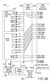
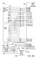
- FIGS. 2A , 2B and 2C schematically illustrate the architecture of a first system 200 using a USB Type-C interface in different operation modes according to an embodiment of the invention.
- the first system 200 is mounted on a printed circuit board (PCB).
- the first system 200 comprises a multi-function control circuit 210, a high speed switch 220, a USB Type-C receptacle 230, a USB power delivery controller 240, a power adaptor 250, a device-to-device power source 260 and plural capacitors c.
- A2 ⁇ A3, A5 ⁇ A8, A10 ⁇ A11, B2 ⁇ B3, B5 ⁇ B8 and B10 ⁇ B11 pins of the USB Type-C receptacle 230 are connected with the high speed switch 220.
- A4, A9, B4 and B9 of the USB Type-C receptacle 230 receive a bus voltage Vbus.
- A1, A12, B1 and B12 pins receives a ground voltage GND.
- the multi-function control circuit 210 comprises a USB controller 212 and a graphics processing unit (GPU) 214.
- the USB controller 212 comprises a first transmitting differential pair (TX1+ and TX1), a second transmitting differential pair (TX2+ and TX2-), a first receiving differential pair (RX1+ and RX1-), a second receiving differential pair (RX2+ and RX2-) and a USB 2.0 data differential pair (D+ and D-).
- the graphics processing unit 214 comprises an auxiliary differential pair (AUX+ and AUX-) and four lanes, including four lane differential pairs (L1+ and L1-, L2+ and L2-, L3+ and L3- and L4+ and L4-) for outputting DisplayPort AV signals.
- the pin corresponding to the single directional output signal has to be serially connected with the 100nF capacitor c, and the pin corresponding to the single directional input signal and the pin corresponding to the bidirectional signal do not need to be serially connected with the capacitors. Consequently, as shown in FIG. 2A , the first transmitting differential pair (TX1+ and TX1) and the second transmitting differential pair (TX2+ and TX2-) of the USB controller 212 and the four lane differential pairs (L1+ and L1-, L2+ and L2-, L3+ and L3- and L4+ and L4-) of the graphics processing unit 214 are coupled with the high speed switch 220 through corresponding capacitors c.
- the first receiving differential pair (RX1+ and RX1-), the second receiving differential pair (RX2+ and RX2-) and the USB 2.0 data differential pair (D+ and D-) of the USB controller 212 and the auxiliary differential pair (AUX+ and AUX-) of the graphics processing unit 214 are directly connected with the high speed switch 220.
- the power adapter 250 is connected with the high speed switch 220 and connected with one of the A5 pin and the B5 pin of the USB Type-C receptacle 230, e.g. the B5 pin.
- the USB power delivery controller 240 is connected with the high speed switch 220 and connected with the other one of the A5 pin and the B5 pin of the USB Type-C receptacle 230, e.g. the A5 pin.
- one of the A5 pin and the B5 pin outputs a configuration channel signal CC, and the other one of the A5 pin and the B5 pin receives a connection voltage Vconn.
- the configuration channel signal CC is transmitted to the USB power delivery controller 240, and the connection voltage Vconn is transmitted to the USB Type-C receptacle 230.
- the first system 200 can realize whether the plugged device is plugged into the USB Type-C receptacle 230 in an up orientation or a down orientation and further realize whether the plugged device is a USB device or a display device.
- the USB power delivery controller 240 is connected with the multi-function control circuit 210 and the power adapter 250. After the device plugged into the USB Type-C receptacle 230 is realized, the USB power delivery controller 240 will control the high speed switch 220 to adjust the switching path. Moreover, the device-to-device power source 260 is connected with the USB power delivery controller 240. The device-to-device power source 260 generates a bus voltage Vbus to the USB Type-C receptacle 230.
- FIG. 2A schematically illustrates the architecture of the first system 200 in a first operation mode according to an embodiment of the invention.
- a USB device is plugged into the USB Type-C receptacle 230.
- the switching path of the high speed switch 220 is adjusted to the USB controller 212.
- the first transmitting differential pair (TX1+ and TX1) of the USB controller 212 is coupled with the USB Type-C receptacle 230 through the corresponding capacitors c; the second transmitting differential pair (TX2+ and TX2-) of the USB controller 212 is coupled with the USB Type-C receptacle 230 through the corresponding capacitors c; the first receiving differential pair (RX1+ and RX1-) of the USB controller 212 is directly connected with the USB Type-C receptacle 230; and the second receiving differential pair (RX2+ and RX2-) of the USB controller 212 is directly connected with the USB Type-C receptacle 230.
- FIG. 2B schematically illustrates the architecture of the first system 200 in a second operation mode according to an embodiment of the invention.
- a display device is plugged into the USB Type-C receptacle 230.
- the first system 200 realizes that the display device is plugged into the USB Type-C receptacle 230. If all lanes need to be used, the switching path of the high speed switch 220 is adjusted to the graphics processing unit 214.
- the B11 pin and the B10 pin of the USB Type-C receptacle 230 are coupled with the first lane differential pair (L1+ and L1-) of the graphics processing unit 214 through the corresponding capacitors c; the B2 pin and the B3 pin of the USB Type-C receptacle 230 are coupled with the second lane differential pair (L2+ and L2-) of the graphics processing unit 214 through the corresponding capacitors c; the A11 pin and the A10 pin of the USB Type-C receptacle 230 are coupled with the third lane differential pair (L3+ and L3-) of the graphics processing unit 214 through the corresponding capacitors c; and the A2 pin and the A3 pin of the USB Type-C receptacle 230 are coupled with the fourth lane differential pair (L4+ and L4-) of the graphics processing unit 214 through the corresponding capacitors c.
- the A8 pin and the B8 pin of the USB Type-C receptacle 230 are connected with the auxiliary differential pair (AUX+ and AUX-) of the graphics processing unit 214. Consequently, the DisplayPort AV signals are outputted to the display device through the four lanes of the graphics processing unit 214.
- FIG. 2C schematically illustrates the architecture of the first system 200 in a third operation mode according to an embodiment of the invention.
- a display device is plugged into the USB Type-C receptacle 230.
- the first system 200 realizes that the display device is plugged into the USB Type-C receptacle 230. If only portions of the lanes need to be used, the switching path of the high speed switch 220 is adjusted to the USB controller 212 and the graphics processing unit 214.
- the A2 pin and the A3 pin of the USB Type-C receptacle 230 are coupled with the first transmitting differential pair (TX1+ and TX1) of the USB controller 212 through the corresponding capacitors; the A11 pin and the A10 pin of the USB Type-C receptacle 230 are coupled with the second receiving differential pair (RX2+ and RX2-) of the USB controller 212; the B11 pin and the B10 pin of the USB Type-C receptacle 230 are coupled with the first lane differential pair (L1+ and L1-) of the graphics processing unit 214 through the corresponding capacitors c; and the B2 pin and the B3 pin of the USB Type-C receptacle 230 are coupled with the second lane differential pair (L2+ and L2-) of the graphics processing unit 214 through the corresponding capacitors c.
- the A8 pin and the B8 pin of the USB Type-C receptacle 230 are connected with the auxiliary differential pair (AUX+ and
- the DisplayPort AV signals are outputted to the display device through the two lanes of the graphics processing unit 214.
- the display device is in communication with the USB controller 212 through the first transmitting differential pair (TX1+ and TX1) and the second transmitting differential pair (TX2+ and TX2-).
- the multi-function control circuit 210 on the printed circuit board has at least twenty pins for inputting and outputting signals. Moreover, the high speed switch 220 is required to provide the switching path. Consequently, the cost of the first system 200 is relatively higher. By modifying the internal connecting relationships of the multi-function control circuit 210, the cost of the overall system can be effectively reduced.
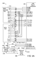
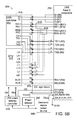
- FIGS. 3A , 3B , 3C and 3D schematically illustrate the architecture of a second system 300 using a USB Type-C interface in different operation modes according to an embodiment of the invention.
- the second system 300 is mounted on a printed circuit board (PCB).
- the second system 300 comprises a multi-function control circuit 310, a USB Type-C receptacle 230, a USB power delivery controller 340, a power adaptor 350, a device-to-device power source 360, a configuration channel logic circuit (CC logic circuit) 370 and plural capacitors c.
- PCB printed circuit board
- the A6 pin and the B6 pin of the USB Type-C receptacle 230 are connected with a first pin 1 of the multi-function control circuit 310.
- the A7 pin and the B7 pin of the USB Type-C receptacle 230 are connected with a second pin 2 of the multi-function control circuit 310.
- the A2 pin of the USB Type-C receptacle 230 is connected with a third pin 3 of the multi-function control circuit 310 through the corresponding capacitor c.
- the A3 pin of the USB Type-C receptacle 230 is connected with a fourth pin 4 of the multi-function control circuit 310 through the corresponding capacitor c.
- the A11 pin of the USB Type-C receptacle 230 is connected with a ninth pin 9 of the multi-function control circuit 310 through the corresponding capacitor c.
- the A10 pin of the USB Type-C receptacle 230 is connected with a tenth pin 10 of the multi-function control circuit 310 through the corresponding capacitor c.
- the B2 pin of the USB Type-C receptacle 230 is connected with a fifth pin 5 of the multi-function control circuit 310 through the corresponding capacitor c.
- the B3 pin of the USB Type-C receptacle 230 is connected with a sixth pin 6 of the multi-function control circuit 310 through the corresponding capacitor c.
- the B11 pin of the USB Type-C receptacle 230 is connected with a seventh pin 7 of the multi-function control circuit 310 through the corresponding capacitor c.
- the B10 pin of the USB Type-C receptacle 230 is connected with an eighth pin 8 of the multi-function control circuit 310 through the corresponding capacitor c.
- the A8 pin of the USB Type-C receptacle 230 is connected with an eleventh pin 11 of the multi-function control circuit 310.
- the B8 pin of the USB Type-C receptacle 230 is connected with a twelfth pin 12 of the multi-function control circuit 310.
- the multi-function control circuit 310 comprises a USB controller 312 and a graphics processing unit (GPU) 314.
- the USB controller 312 comprises a USB 2.0 data differential pair (D+ and D-), a first transmitting differential pair (TX1+ and TX1), a second transmitting differential pair (TX2+ and TX2-), a first receiving differential pair (RX1+ and RX1-) and a second receiving differential pair (RX2+ and RX2-).
- the USB 2.0 data differential pair (D+ and D-) is connected with the first pin 1 and the second pin 2.
- the first transmitting differential pair (TX1+ and TX1) is connected with the third pin 3 and the fourth pin 4.
- the second transmitting differential pair (TX2+ and TX2-) is connected with the fifth pin 5 and the sixth pin 6.
- the first receiving differential pair (RX1+ and RX1-) is connected with the seventh pin 7 and the eighth pin 8.
- the second receiving differential pair (RX2+ and RX2-) is connected with the ninth pin 9 and the tenth pin 10.
- the graphics processing unit 314 comprises an auxiliary differential pair (AUX+ and AUX-) and four lanes, including four lane differential pairs (L1+ and L1-, L2+ and L2-, L3+ and L3- and L4+ and L4-) for outputting DisplayPort AV signals.
- the first lane differential pair (L1+ and L1-) is connected with the third pin 3 and the fourth pin 4.
- the second lane differential pair (L2+ and L2-) is connected with the fifth pin 5 and the sixth pin 6.
- the third lane differential pair (L3+ and L3-) is connected with the seventh pin 7 and the eighth pin 8.
- the fourth lane differential pair (L4+ and L4-) is connected with the ninth pin 9 and the tenth pin 10.
- the auxiliary differential pair (AUX+ and AUX-) is connected with the eleventh pin 11 and the twelfth pin 12.
- the power adapter 350 is connected with one of the A5 pin and the B5 pin of the USB Type-C receptacle 230 (e.g., the B5 pin) through the configuration channel logic circuit 370.
- the USB power delivery controller 340 is connected with the other one of the A5 pin and the B5 pin of the USB Type-C receptacle 230 (e.g., the A5 pin) through the configuration channel logic circuit 370.
- one of the A5 pin and the B5 pin acts as configuration channel signal CC, and the other one of the A5 pin and the B5 pin will be used for Vconn voltage.
- the configuration channel signal CC is transmitted to the USB power delivery controller 340, and the connection voltage Vconn is transmitted to the USB Type-C receptacle 230.
- the second system 300 can realize whether the plugged device is plugged into the USB Type-C receptacle 230 in an up orientation or a down orientation and further realize whether the plugged device is a USB device or a display device.
- the USB power delivery controller 340 is connected with the multi-function control circuit 310 and the power adapter 350.
- the device-to-device power source 260 generates a bus voltage Vbus to the USB Type-C receptacle 230.
- FIG. 3B schematically illustrates the architecture of the second system 300 in a first operation mode according to an embodiment of the invention.
- a USB device is plugged into the USB Type-C receptacle 230.
- the graphics processing unit 314 does not generate any output signal.
- the first transmitting differential pair (TX1+ and TX1) of the USB controller 312 is coupled with the USB Type-C receptacle 230 through the corresponding capacitors c; the second transmitting differential pair (TX2+ and TX2-) of the USB controller 312 is coupled with the USB Type-C receptacle 230 through the corresponding capacitors c; the first receiving differential pair (RX1+ and RX1-) of the USB controller 312 is directly connected with the USB Type-C receptacle 230; and the second receiving differential pair (RX2+ and RX2-) of the USB controller 312 is directly connected with the USB Type-C receptacle 230. Consequently, the USB device can receive all signals from the USB controller 312.
- FIG. 3C schematically illustrates the architecture of the second system 300 in a second operation mode according to an embodiment of the invention.
- a display device is plugged into the USB Type-C receptacle 230.
- the second system 300 realizes that the display device is plugged into the USB Type-C receptacle 230. If all lanes need to be used, the USB controller 312 does not generate any output signal.
- the A2 pin and the A3 pin of the USB Type-C receptacle 230 are coupled with the first lane differential pair (L1+ and L1-) of the graphics processing unit 314 through the corresponding capacitors c; the B2 pin and the B3 pin of the USB Type-C receptacle 230 are coupled with the second lane differential pair (L2+ and L2-) of the graphics processing unit 314 through the corresponding capacitors c; the B11 pin and the B10 pin of the USB Type-C receptacle 230 are coupled with the third lane differential pair (L3+ and L3-) of the graphics processing unit 314 through the corresponding capacitors c; and the A11 pin and the A10 pin of the USB Type-C receptacle 230 are coupled with the fourth lane differential pair (L4+ and L4-) of the graphics processing unit 314 through the corresponding capacitors c.
- the A8 pin and the B8 pin of the USB Type-C receptacle 230 are connected with the auxiliary differential pair (AUX+ and AUX-) of the graphics processing unit 314. Consequently, the DisplayPort AV signals are outputted to the display device through the four lanes of the graphics processing unit 314.
- FIG. 3D schematically illustrates the architecture of the second system 300 in a third operation mode according to an embodiment of the invention.
- a display device is plugged into the USB Type-C receptacle 230.
- the second system 300 realizes that the display device is plugged into the USB Type-C receptacle 230. If only portions of the lanes need to be used, the second transmitting differential pair (TX2+ and TX2-) and the first receiving differential pair (RX1+ and RX1-) of the USB controller 312 are inactivated, and the first lane differential pair (L1+ and L1-) and the fourth lane differential pair (L4+ and L4-) of the graphics processing unit 314 are inactivated.
- the A2 pin and the A3 pin of the USB Type-C receptacle 230 are coupled with the first transmitting differential pair (TX1+ and TX1) of the USB controller 312 through the corresponding capacitors; the A11 pin and the A10 pin of the USB Type-C receptacle 230 are coupled with the second receiving differential pair (RX2+ and RX2-) of the USB controller 312 through the corresponding capacitors; the B11 pin and the B10 pin of the USB Type-C receptacle 230 are coupled with the third lane differential pair (L3+ and L3-) of the graphics processing unit 314 through the corresponding capacitors c; and the B2 pin and the B3 pin of the USB Type-C receptacle 230 are coupled with the second lane differential pair (L2+ and L2-) of the graphics processing unit 314 through the corresponding capacitors c.
- the A8 pin and the B8 pin of the USB Type-C receptacle 230 are connected with the auxiliary differential pair
- the DisplayPort AV signals are outputted to the display device through the two lanes of the graphics processing unit 314.
- the display device is in communication with the USB controller 312 through the first transmitting differential pair (TX1+ and TX1) and the second transmitting differential pair (TX2+ and TX2-).
- the multi-function control circuit 310 of the second system 300 on the printed circuit board has only twelve pins for inputting and outputting signals. Moreover, the second system 300 does not require the high speed switch. Consequently, the cost of the second system 300 is reduced, and the area of the printed circuit board is effectively reduced.
- the pin corresponding to the single directional output signal has to be serially connected with the capacitor c and the capacitance value of the capacitor c is between 75nF and 275nF, such as 100nF. Furthermore, the pin corresponding to the single directional input signal and the pin corresponding to the bidirectional signal do not need to be serially connected with the capacitors.
- the first receiving differential pair (RX1+ and RX1-) and the second receiving differential pair (RX2+ and RX2-) are also coupled with the corresponding capacitors c. In the worst situation, the signal distortion problem may occur, and thus the receiver of the USB controller 312 may abnormally work.
- FIGS. 4A and 4B two examples of the USB controller 312 will be illustrated with reference to FIGS. 4A and 4B .
- FIG. 4A is a schematic circuit diagram illustrating a portion of an exemplary USB controller 312 of the second system 300 of the invention.
- first receiving differential pair (RX1+ and RX1-) of the USB controller 312 is shown in the drawing.
- the similar circuit can be applied to the second receiving differential pair (RX2+ and RX2-) of the USB controller 312, and is not redundantly described herein.
- the receiver of the USB controller 312 is equipped with a termination logic circuit 315 for changing the resistance values of terminal resistors so as to change the RC constant.
- the termination logic circuit 315 of the USB controller 312 generates a switching signal Csw to a switching circuit.
- the switch circuit comprises two switching elements 316 and 318. In a normal working state, the switching elements 316 and 318 are connected with a first resistor r1 in response to the switching signal Csw, and thus the first receiving differential pair (RX1+ and RX1-) is connected with the first resistor r1. In a triggering state, the switching elements 316 and 318 are connected with a second resistor r2 in response to the switching signal Csw.
- the resistance value of the terminal resistor is about 50 ohms.
- the resistance value of the first resistor r1 is smaller than the resistance value of the second resistor r2.
- the resistance value of the first resistor r1 is 50 ohms
- the resistance value of the second resistor r2 is 100 ohms.
- the multi-function control circuit 310 is powered on or reset, a device is plugged into the USB Type-C receptacle 230, a device is detached from the USB Type-C receptacle 230 or the first receiving differential pair (RX1+ and RX1-) is in a signal silent condition, the USB controller 312 is in the triggering state. Under this circumstance, the switching elements 316 and 318 are connected with the second resistor r2 in response to the switching signal Csw.
- the USB controller 312 is in the normal working state. Under this circumstance, the switching elements 316 and 318 are connected with the second resistor r1 in response to the switching signal Csw.
- the time constant RC is increased. Under this circumstance, the signal in the first receiving differential pair (RX1+ and RX1-) is not suffered from distortion, so that the signal is detected easily. After the signal in the first receiving differential pair (RX1+ and RX1-) is detected, the first receiving differential pair (RX1+ and RX1-) is connected with the first resistor r1. Consequently, the USB controller 312 is in the normal working state.
- the second system 300 further comprises a common mode voltage control circuit 320.
- the common mode voltage control circuit 320 is arranged between two capacitors for stabilizing the common mode voltage.
- the common mode voltage control circuit 320 comprises two third resistors r3.
- the two third resistors r3 are serially connected between the two capacitors.
- the node between the two third resistors r3 is connected to the ground voltage.
- FIG. 4B is a schematic circuit diagram illustrating a portion of an exemplary USB controller 312 of the second system 300 of the invention.
- first receiving differential pair (RX1+ and RX1-) and the first transmitting differential pair (TX1+ and TX1) of the USB controller 312 are shown in the drawing.
- the similar circuit can be applied to the second receiving differential pair (RX2+ and RX2-) and the second transmitting differential pair (TX2+ and TX2-) of the USB controller 312, and is not redundantly described herein.
- the first transmitting differential pair (TX1 + and TX1) of the USB controller 312 of the multi-function control circuit 310 has to be serially connected with the 100nF capacitors c. Moreover, the first receiving differential pair (RX1+ and RX1-) of the USB controller 312 of the multi-function control circuit 310 does not need to be connected with the capacitors. If the first receiving differential pair (RX1+ and RX1-) is serially connected with the capacitors c, the time constant RC is reduced. In the worst situation, the signal distortion problem may occur, and thus the signal cannot be successfully detected.
- the layout trace of the first receiving differential pair (RX1+ and RX1-) on the printed circuit board has a lower equivalent capacitance value, the reduction of the time constant RC become more obvious.
- the first receiving differential pair (RX1+ and RX1-) is coupled with capacitors C with higher capacitance values.
- the capacitance value of the capacitor C is 400nF. Consequently, the reduction of the time constant RC of the first receiving differential pair (RX1+ and RX1-) is not obvious. Under this circumstance, the signal in the first receiving differential pair (RX1+ and RX1-) can be successfully detected.
- FIGS. 5A , 5B , 5C and 5D schematically illustrate the architecture of a third system using a USB Type-C interface in different operation modes according to an embodiment of the invention.
- the third system 500 is mounted on a printed circuit board (PCB).
- the third system 500 comprises a multi-function control circuit 510, a USB Type-C receptacle 230, a first path switching circuit (SW1) 516, a second path switching circuit (SW2) 518, a USB power delivery controller 340, a power adaptor 350, a device-to-device power source 360, a configuration channel logic circuit (CC logic circuit) 370 and plural capacitors c.
- the operations of the USB power delivery controller 340, the power adaptor 350, the device-to-device power source 360 and the configuration channel logic circuit 370 are identical to those of the second system 300, and are not redundantly described herein.
- the A6 pin and the B6 pin of the USB Type-C receptacle 230 are connected with a first pin 1 of the multi-function control circuit 510.
- the A7 pin and the B7 pin of the USB Type-C receptacle 230 are connected with a second pin 2 of the multi-function control circuit 510.
- the A2 pin of the USB Type-C receptacle 230 is connected with a third pin 3 of the multi-function control circuit 510 through the corresponding capacitor c.
- the A3 pin of the USB Type-C receptacle 230 is connected with a fourth pin 4 of the multi-function control circuit 510 through the corresponding capacitor c.
- the B2 pin of the USB Type-C receptacle 230 is connected with a fifth pin 5 of the multi-function control circuit 510 through the corresponding capacitor c.
- the B3 pin of the USB Type-C receptacle 230 is connected with a sixth pin 6 of the multi-function control circuit 510 through the corresponding capacitor c.
- the A8 pin of the USB Type-C receptacle 230 is connected with a fifteenth pin 15 of the multi-function control circuit 510.
- the B8 pin of the USB Type-C receptacle 230 is connected with a sixteenth pin 16 of the multi-function control circuit 510.
- the B11 pin and the B10 pin of the USB Type-C receptacle 230 are connected with the first path switching circuit 516.
- the A11 pin and the A10 pin of the USB Type-C receptacle 230 are connected with the second path switching circuit 518.
- the first path switching circuit 516 is further connected with a seventh pin 7 and an eighth pin 8 of the multi-function control circuit 510, and coupled with an eleventh pin 11 and a twelfth pin 12 of the multi-function control circuit 510 through the corresponding capacitors c.
- the second path switching circuit 518 is further connected with a ninth pin 9 and a tenth pin 10 of the multi-function control circuit 510, and coupled with a thirteenth pin 13 and a fourteenth pin 14 of the multi-function control circuit 510 through the corresponding capacitors c.
- the multi-function control circuit 510 comprises a USB controller 512 and a graphics processing unit (GPU) 514.
- the USB controller 512 comprises a USB 2.0 data differential pair (D+ and D-), a first transmitting differential pair (TX1+ and TX1), a second transmitting differential pair (TX2+ and TX2-), a first receiving differential pair (RX1+ and RX1-) and a second receiving differential pair (RX2+ and RX2-).
- the USB 2.0 data differential pair (D+ and D-) is connected with the first pin 1 and the second pin 2.
- the first transmitting differential pair (TX1+ and TX1) is connected with the third pin 3 and the fourth pin 4.
- the second transmitting differential pair (TX2+ and TX2-) is connected with the fifth pin 5 and the sixth pin 6.
- the first receiving differential pair (RX1+ and RX1-) is connected with the seventh pin 7 and the eighth pin 8.
- the second receiving differential pair (RX2+ and RX2-) is connected with the fifteenth pin 15 and the eighth pin 10.
- the graphics processing unit 514 comprises an auxiliary differential pair (AUX+ and AUX-) and four lanes.
- the four lanes are four lane differential pairs (L1+ and L1-, L2+ and L2-, L3+ and L3- and L4+ and L4-).
- the first lane differential pair (L1+ and L1-) is connected with the eleventh pin 11 and the twelfth pin 12.
- the second lane differential pair (L2+ and L2-) is connected with the thirteenth pin 13 and the fourteenth pin 14.
- the third lane differential pair (L3+ and L3-) is connected with the third pin 3 and the fourth pin 4.
- the fourth lane differential pair (L4+ and L4-) is connected with the fifth pin 5 and the sixth pin 6.
- the auxiliary differential pair (AUX+ and AUX-) is connected with the fifteenth pin 15 and the sixteenth pin 16.
- FIG. 5B schematically illustrates the architecture of the third system in a first operation mode according to an embodiment of the invention.
- a USB device is plugged into the USB Type-C receptacle 230.
- the graphics processing unit 514 does not generate any output signal.
- the first receiving differential pair (RX1+ and RX1-) and the second receiving differential pair (RX2+ and RX2-) are connected with the USB Type-C receptacle 230 through the first path switching circuit 516 and the second path switching circuit 518.
- the first transmitting differential pair (TX1+ and TX1) and the second transmitting differential pair (TX2+ and TX2-) of the USB controller 512 are coupled with the corresponding pins of the USB Type-C receptacle 230 through the corresponding capacitors c, and the first receiving differential pair (RX1 + and RX1-) and the second receiving differential pair (RX2+ and RX2-) of the USB controller 512 are connected with the corresponding pins of the USB Type-C receptacle 230 through the first path switching circuit 516 and the second path switching circuit 518. Consequently, the USB device can receive all signals from the USB controller 512. Moreover, the first path switching circuit 516 and the second path switching circuit 518 are controlled by the multi-function control circuit 510 or the configuration channel logic circuit 370. The detailed descriptions thereof are omitted herein.
- FIG. 5C schematically illustrates the architecture of the third system in a second operation mode according to an embodiment of the invention.
- a display device is plugged into the USB Type-C receptacle 230.
- the third system 500 realizes that the display device is plugged into the USB Type-C receptacle 230. If all lanes need to be used, the USB controller 512 does not generate any output signal. Under this circumstance, the first lane differential pair (L1+ and L1-) and the second lane differential pair (L2+ and L2-) of the graphics processing unit 514 are coupled with the USB Type-C receptacle 230 through the first path switching circuit 516 and the second path switching circuit 518 and the corresponding capacitors c.
- the B11 pin and the B10 pin of the USB Type-C receptacle 230 are coupled with the first lane differential pair (L1+ and L1-) of the graphics processing unit 514 through the corresponding capacitors c; the B2 pin and the B3 pin of the USB Type-C receptacle 230 are coupled with the fourth lane differential pair (L4+ and L4-) of the graphics processing unit 514 through the corresponding capacitors c; the A11 pin and the A10 pin of the USB Type-C receptacle 230 are coupled with the second lane differential pair (L2+ and L2-) of the graphics processing unit 514 through the corresponding capacitors c; and the A2 pin and the A3 pin of the USB Type-C receptacle 230 are coupled with the third lane differential pair (L3+ and L3-) of the graphics processing unit 514 through the corresponding capacitors c.
- the A8 pin and the B8 pin of the USB Type-C receptacle 230 are connected with the auxiliary differential pair (AUX+ and AUX-) of the graphics processing unit 514. Consequently, the DisplayPort AV signals are outputted to the display device through the four lanes of the graphics processing unit 514.
- FIG. 5D schematically illustrates the architecture of the third system in a third operation mode according to an embodiment of the invention.
- a display device is plugged into the USB Type-C receptacle 230.
- the third system 500 realizes that the display device is plugged into the USB Type-C receptacle 230. If only portions of the lanes need to be used, the second transmitting differential pair (TX2+ and TX2-) and the first receiving differential pair (RX1+ and RX1-) of the USB controller 512 are inactivated, and the second lane differential pair (L2+ and L2-) and the third lane differential pair (L3+ and L3-) of the graphics processing unit 514 are inactivated.
- the first lane differential pair (L1+ and L1-) is coupled with the USB Type-C receptacle 230 through the first path switching circuit 516 and the corresponding capacitors c; and the second receiving differential pair (RX2+ and RX2-) is connected with the USB Type-C receptacle 230 through the second path switching circuit 518.
- the A2 pin and the A3 pin of the USB Type-C receptacle 230 are coupled with the first transmitting differential pair (TX1+ and TX1) of the USB controller 512 through the corresponding capacitors c; the A11 pin and the A10 pin are connected with the second receiving differential pair (RX2+ and RX2-); the B11 pin and the B10 pin are coupled with the first lane differential pair (L1+ and L1-) through the corresponding capacitors c; and the B2 pin and the B3 pin are coupled with the fourth lane differential pair (L4+ and L4-) of the graphics processing unit 514 through the corresponding capacitors c.
- the A8 pin and the B8 pin of the USB Type-C receptacle 230 are connected with the auxiliary differential pair (AUX+ and AUX-) of the graphics processing unit 514.
- the DisplayPort AV signals are outputted to the display device through the two lanes of the graphics processing unit 514.
- the display device is in communication with the USB controller 512 through the first transmitting differential pair (TX1+ and TX1) and the second transmitting differential pair (TX2+ and TX2-).
- the multi-function control circuit 510 of the third system 500 on the printed circuit board has only sixteen pins for inputting and outputting signals. Moreover, the third system 500 is not equipped with the high speed switch. Consequently, the cost of the third system 500 is reduced, and the area of the printed circuit board is effectively reduced.
- the USB power delivery controller 340, the power adaptor 350, the device-to-device power source 360 and the configuration channel logic circuit 370 are individual circuits or control into the multi-function control circuit. Moreover, the sequence of the four lane differential pairs of the graphics processing unit is not restricted.
- the invention provides a system using a USB Type-C interface.
- This system not only transmits the normal USB signal but also supports a DisplayPort Alternate Mode.
- the cost of the overall system is reduced, and the area of the printed circuit board is effectively reduced.
Landscapes
- Engineering & Computer Science (AREA)
- Theoretical Computer Science (AREA)
- Physics & Mathematics (AREA)
- General Engineering & Computer Science (AREA)
- General Physics & Mathematics (AREA)
- Information Transfer Systems (AREA)
- Power Sources (AREA)
- Microelectronics & Electronic Packaging (AREA)
Abstract
Description
- The invention relates to a system and a circuit using a USB interface, and more particularly to a system and a circuit using a USB Type-C interface.
-
FIG. 1 schematically illustrates a USB Type-C interface 100. The USB Type-C interface 100 is a USB Type-C receptacle. The pins of the USB Type-C receptacle 100 comprise A group pins (A1∼A12) and B group pins (B1∼B12). The A1 pin, the A12 pin, the B1 pin and the B12 pin are ground voltage pins (GND); the A4 pin, the A9 pin, the B4 pin and the B9 pin are bus voltage pins (Vbus); the A2 pin and the A3 pin are a first transmitting differential pair (TX1 + and TX1); the B2 pin and the B3 pin are a second transmitting differential pair (TX2+ and TX2-); the B10 pin and the B11 pin are a first receiving differential pair (RX1+ and RX1-); the A10 pin and the A11 pin are a second receiving differential pair (RX2+ and RX2-); the A6 pin and the A7 pin are a USB 2.0 data differential pair (D+ and D-); the B6 pin and the B7 pin are also a USB 2.0 data differential pair (D+ and D-); the A5 pin and the B5 pin are configuration channel pins (CC1 and CC2); and the A8 and B8 are reserved pins (SBU1 and SBU2). - Moreover, the first transmitting differential pair (TX1+ and TX1), the second transmitting differential pair (TX2+ and TX2-), the first receiving differential pair (RX1+ and RX1-) and the second receiving differential pair (RX2+ and RX2-) are capable of carrying USB 3.1 differential signals.
- As shown in
FIG. 1 , A group pins (A1∼A12) and B group pins of the USB Type-C receptacle 100 are symmetrical. When a USB device is plugged into the USB Type-C receptacle 100 in an up orientation or a down orientation, the USB device can normally work. For example, when the USB device is plugged into the USB Type-C receptacle 100 in the up orientation, the USB device is connected with the A group pins, and the USB Type-C receptacle 100 is in communication with the USB device through the A group pins. On the other hand, when the USB device is plugged into the USB Type-C receptacle 100 in the down orientation, the USB device is connected with the B group pins, and the USB Type-C receptacle 100 is in communication with the USB device through the B group pins. - Furthermore, the USB Type-C interface can be used as the connection interface of other device such as a power device, a data device or a display device. For example, when the display device with PCIe interface is plugged into the USB Type-C receptacle, PCIe interface signals can be transmitted through the pins of the USB Type-C receptacle. This is the concept of PCIe over USB.
- An object of the invention provides a system and a circuit using a USB Type-C interface. This system not only transmits the normal USB signal but also supports a DisplayPort Alternate Mode. In the DisplayPort Alternate Mode, the USB Type-C interface provides the pins of the DisplayPort.
- The invention provides a system using a USB Type-C interface. The system includes a multi-function control circuit and a USB Type-C receptacle. The multi-function control circuit is mounted on a printed circuit board, and includes a USB controller and a graphics processing unit. The USB controller includes a data differential pair, a first transmitting differential pair, a second transmitting differential pair, a first receiving differential pair and a second receiving differential pair. The data differential pair is connected with a first pin and a second pin of the multi-function control circuit. The first transmitting differential pair is connected with a third pin and a fourth pin of the multi-function control circuit. The second transmitting differential pair is connected with a fifth pin and a sixth pin of the multi-function control circuit. The first receiving differential pair is connected with a seventh pin and an eighth pin of the multi-function control circuit. The second receiving differential pair is connected with a ninth pin and a tenth pin of the multi-function control circuit. The graphics processing unit includes a first lane differential pair, a second lane differential pair, a third lane differential pair, a fourth lane differential pair and an auxiliary differential pair. The first lane differential pair is connected with the third pin and the fourth pin of the multi-function control circuit. The second lane differential pair is connected with the fifth pin and the sixth pin of the multi-function control circuit. The third lane differential pair is connected with the seventh pin and the eighth pin of the multi-function control circuit. The fourth lane differential pair is connected with the ninth pin and the ten pin of the multi-function control circuit. The auxiliary differential pair is connected with an eleventh pin and a twelfth pin of the multi-function control circuit. The USB Type-C receptacle is mounted on a printed circuit board, and includes plural pins. An A1 pin is connected with a ground voltage, an A2 pin is coupled with the third pin through a first capacitor, an A3 pin is coupled with the fourth pin through a second capacitor, an A4 pin is connected with a bus voltage, an A6 pin is connected with the first pin, an A7 pin is connected with the second pin, an A9 pin is connected with the bus voltage, an A10 pin is coupled with the tenth pin through a third capacitor, an A11 pin is coupled with the ninth pin through a fourth capacitor, an A12 pin is connected with the ground voltage. A B1 pin is connected with the ground voltage, a B2 pin is coupled with the fifth pin through a fifth capacitor, a B3 pin is coupled with the sixth pin through a sixth capacitor, a B4 pin is connected with the bus voltage, a B6 pin is connected with the first pin, a B7 pin is connected with the second pin, a B9 pin is connected with the bus voltage, a B10 pin is connected with the eighth pin through a seventh capacitor, a B11 pin is connected with the seventh pin through an eighth capacitor, and a B12 pin is connected with the ground voltage. Moreover, an A8 pin is connected with the eleventh pin, a B8 pin is connected with the twelfth pin, one of an A5 pin and a B5 pin provides a configuration channel signal, and the other one of the A5 pin and the B5 pin receives a connection voltage.
- The invention further provides a multi-function control circuit. The multi-function control circuit includes a USB controller and a graphics processing unit. The USB controller includes a data differential pair, a first transmitting differential pair, a second transmitting differential pair, a first receiving differential pair and a second receiving differential pair. The data differential pair is connected with a first pin and a second pin of the multi-function control circuit. The first transmitting differential pair is connected with a third pin and a fourth pin of the multi-function control circuit. The second transmitting differential pair is connected with a fifth pin and a sixth pin of the multi-function control circuit. The first receiving differential pair is connected with a seventh pin and an eighth pin of the multi-function control circuit. The second receiving differential pair is connected with a ninth pin and a tenth pin of the multi-function control circuit. The graphics processing unit includes a first lane differential pair, a second lane differential pair, a third lane differential pair, a fourth lane differential pair and an auxiliary differential pair. The first lane differential pair is connected with the third pin and the fourth pin of the multi-function control circuit. The second lane differential pair is connected with the fifth pin and the sixth pin of the multi-function control circuit. The third lane differential pair is connected with the seventh pin and the eighth pin of the multi-function control circuit. The fourth lane differential pair is connected with the ninth pin and the ten pin of the multi-function control circuit. The auxiliary differential pair is connected with an eleventh pin and a twelfth pin of the multi-function control circuit.
- The invention further provides a system using a USB Type-C interface. The system includes a multi-function control circuit, a first path switching circuit, a second path switching circuit and a USB Type-C receptacle. The multi-function control circuit is mounted on a printed circuit board, and includes a USB controller and a graphics processing unit. The USB controller includes a data differential pair, a first transmitting differential pair, a second transmitting differential pair, a first receiving differential pair and a second receiving differential pair. The data differential pair is connected with a first pin and a second pin of the multi-function control circuit. The first transmitting differential pair is connected with a third pin and a fourth pin of the multi-function control circuit. The second transmitting differential pair is connected with a fifth pin and a sixth pin of the multi-function control circuit. The first receiving differential pair is connected with a seventh pin and an eighth pin of the multi-function control circuit. The second receiving differential pair is connected with a ninth pin and a tenth pin of the multi-function control circuit. The graphics processing unit includes a first lane differential pair, a second lane differential pair, a third lane differential pair, a fourth lane differential pair and an auxiliary differential pair. The first lane differential pair is connected with an eleventh pin and a twelfth pin of the multi-function control circuit. The second lane differential pair is connected with a thirteenth pin and a fourteenth pin of the multi-function control circuit. The third lane differential pair is connected with the third pin and the fourth pin of the multi-function control circuit. The fourth lane differential pair is connected with the fifth pin and the sixth pin of the multi-function control circuit. The auxiliary differential pair is connected with a fifteenth pin and a sixteenth pin of the multi-function control circuit. The first path switching circuit is connected with the seventh pin and the eighth pin, and coupled with the eleventh pin and the twelfth pin through a first capacitor and a second capacitor. The second path switching circuit is connected with the ninth pin and the tenth pin, and coupled with the thirteenth pin and the fourteenth pin through a third capacitor and a fourth capacitor. The USB Type-C receptacle is mounted on a printed circuit board, and comprising plural pins. An A1 pin is connected with a ground voltage, an A2 pin is coupled with the third pin through a fifth capacitor, an A3 pin is coupled with the fourth pin through a sixth capacitor, an A4 pin is connected with a bus voltage, an A6 pin is connected with the first pin, an A7 pin is connected with the second pin, an A9 pin is connected with the bus voltage, an A10 pin and an A11 pin are connected with the second path switching circuit, and A12 pin is connected with the ground voltage. A B1 pin is connected with the ground voltage, a B2 pin is coupled with the fifth pin through a seventh capacitor, a B3 pin is coupled with the sixth pin through an eighth capacitor, a B4 pin is connected with the bus voltage, a B6 pin is connected with the first pin, a B7 pin is connected with the second pin, a B9 pin is connected with the bus voltage, a B10 pin and a B11 pin is connected with the first path switching circuit, and a B12 pin is connected with the ground voltage. Moreover, an A8 pin is connected with the fifteenth pin, a B8 pin is connected with the sixteenth pin, one of an A5 pin and a B5 pin provides a configuration channel signal, and the other one of the A5 pin and the B5 pin receives a connection voltage.
- The invention further provides a multi-function control circuit. The multi-function control circuit includes a USB controller and a graphics processing unit. The USB controller includes a data differential pair, a first transmitting differential pair, a second transmitting differential pair, a first receiving differential pair and a second receiving differential pair. The data differential pair is connected with a first pin and a second pin of the multi-function control circuit. The first transmitting differential pair is connected with a third pin and a fourth pin of the multi-function control circuit. The second transmitting differential pair is connected with a fifth pin and a sixth pin of the multi-function control circuit. The first receiving differential pair is connected with a seventh pin and an eighth pin of the multi-function control circuit. The second receiving differential pair is connected with a ninth pin and a tenth pin of the multi-function control circuit. The graphics processing unit includes a first lane differential pair, a second lane differential pair, a third lane differential pair, a fourth lane differential pair and an auxiliary differential pair. The first lane differential pair is connected with an eleventh pin and a twelfth pin of the multi-function control circuit. The second lane differential pair is connected with a thirteenth pin and a fourteenth pin of the multi-function control circuit. The third lane differential pair is connected with the third pin and the fourth pin of the multi-function control circuit. The fourth lane differential pair is connected with the fifth pin and the sixth pin of the multi-function control circuit. The auxiliary differential pair is connected with a fifteenth pin and a sixteenth pin of the multi-function control circuit.
- The above objects and advantages of the invention will become more readily apparent to those ordinarily skilled in the art after reviewing the following detailed description and accompanying drawings, in which:
-
FIG. 1 (prior art) schematically illustrates a USB Type-C interface; -
FIGS. 2A ,2B and2C schematically illustrate the architecture of a first system using a USB Type-C interface in different operation modes according to an embodiment of the invention; -
FIGS. 3A ,3B ,3C and3D schematically illustrate the architecture of a second system using a USB Type-C interface in different operation modes according to an embodiment of the invention; -
FIG. 4A is a schematic circuit diagram illustrating a portion of an exemplary USB controller of the second system of the invention; -
FIG. 4B is a schematic circuit diagram illustrating a portion of another exemplary USB controller of the second system of the invention; and -
FIGS. 5A ,5B ,5C and5D schematically illustrate the architecture of a third system using a USB Type-C interface in different operation modes according to an embodiment of the invention. - As mentioned above, the USB Type-C interface can be used as the connection interface of other device. Therefore, the invention provides a system using a USB Type-C interface. The system supports a DisplayPort Alternate Mode. That is, a display device can receive DisplayPort AV signals through the USB Type-C interface.
-
FIGS. 2A ,2B and2C schematically illustrate the architecture of afirst system 200 using a USB Type-C interface in different operation modes according to an embodiment of the invention. Thefirst system 200 is mounted on a printed circuit board (PCB). Moreover, thefirst system 200 comprises amulti-function control circuit 210, ahigh speed switch 220, a USB Type-C receptacle 230, a USBpower delivery controller 240, a power adaptor 250, a device-to-device power source 260 and plural capacitors c. - A2∼A3, A5∼A8, A10∼A11, B2∼B3, B5∼B8 and B10∼B11 pins of the USB Type-
C receptacle 230 are connected with thehigh speed switch 220. A4, A9, B4 and B9 of the USB Type-C receptacle 230 receive a bus voltage Vbus. A1, A12, B1 and B12 pins receives a ground voltage GND. - The
multi-function control circuit 210 comprises aUSB controller 212 and a graphics processing unit (GPU) 214. TheUSB controller 212 comprises a first transmitting differential pair (TX1+ and TX1), a second transmitting differential pair (TX2+ and TX2-), a first receiving differential pair (RX1+ and RX1-), a second receiving differential pair (RX2+ and RX2-) and a USB 2.0 data differential pair (D+ and D-). Thegraphics processing unit 214 comprises an auxiliary differential pair (AUX+ and AUX-) and four lanes, including four lane differential pairs (L1+ and L1-, L2+ and L2-, L3+ and L3- and L4+ and L4-) for outputting DisplayPort AV signals. - According to the specifications, the pin corresponding to the single directional output signal has to be serially connected with the 100nF capacitor c, and the pin corresponding to the single directional input signal and the pin corresponding to the bidirectional signal do not need to be serially connected with the capacitors. Consequently, as shown in
FIG. 2A , the first transmitting differential pair (TX1+ and TX1) and the second transmitting differential pair (TX2+ and TX2-) of theUSB controller 212 and the four lane differential pairs (L1+ and L1-, L2+ and L2-, L3+ and L3- and L4+ and L4-) of thegraphics processing unit 214 are coupled with thehigh speed switch 220 through corresponding capacitors c. Moreover, the first receiving differential pair (RX1+ and RX1-), the second receiving differential pair (RX2+ and RX2-) and the USB 2.0 data differential pair (D+ and D-) of theUSB controller 212 and the auxiliary differential pair (AUX+ and AUX-) of thegraphics processing unit 214 are directly connected with thehigh speed switch 220. - The power adapter 250 is connected with the
high speed switch 220 and connected with one of the A5 pin and the B5 pin of the USB Type-C receptacle 230, e.g. the B5 pin. The USBpower delivery controller 240 is connected with thehigh speed switch 220 and connected with the other one of the A5 pin and the B5 pin of the USB Type-C receptacle 230, e.g. the A5 pin. Generally, after a USB device or a display device is plugged into the USB Type-C receptacle 230, one of the A5 pin and the B5 pin outputs a configuration channel signal CC, and the other one of the A5 pin and the B5 pin receives a connection voltage Vconn. Through the switching path of thehigh speed switch 220, the configuration channel signal CC is transmitted to the USBpower delivery controller 240, and the connection voltage Vconn is transmitted to the USB Type-C receptacle 230. Moreover, according to the configuration channel signal CC, thefirst system 200 can realize whether the plugged device is plugged into the USB Type-C receptacle 230 in an up orientation or a down orientation and further realize whether the plugged device is a USB device or a display device. - The USB
power delivery controller 240 is connected with themulti-function control circuit 210 and the power adapter 250. After the device plugged into the USB Type-C receptacle 230 is realized, the USBpower delivery controller 240 will control thehigh speed switch 220 to adjust the switching path. Moreover, the device-to-device power source 260 is connected with the USBpower delivery controller 240. The device-to-device power source 260 generates a bus voltage Vbus to the USB Type-C receptacle 230. -
FIG. 2A schematically illustrates the architecture of thefirst system 200 in a first operation mode according to an embodiment of the invention. For example, a USB device is plugged into the USB Type-C receptacle 230. After thefirst system 200 realizes that the USB device is plugged into the USB Type-C receptacle 230 according to the configuration channel signal CC, the switching path of thehigh speed switch 220 is adjusted to theUSB controller 212. Under this circumstance, the first transmitting differential pair (TX1+ and TX1) of theUSB controller 212 is coupled with the USB Type-C receptacle 230 through the corresponding capacitors c; the second transmitting differential pair (TX2+ and TX2-) of theUSB controller 212 is coupled with the USB Type-C receptacle 230 through the corresponding capacitors c; the first receiving differential pair (RX1+ and RX1-) of theUSB controller 212 is directly connected with the USB Type-C receptacle 230; and the second receiving differential pair (RX2+ and RX2-) of theUSB controller 212 is directly connected with the USB Type-C receptacle 230. -
FIG. 2B schematically illustrates the architecture of thefirst system 200 in a second operation mode according to an embodiment of the invention. For example, a display device is plugged into the USB Type-C receptacle 230. According to the configuration channel signal CC, thefirst system 200 realizes that the display device is plugged into the USB Type-C receptacle 230. If all lanes need to be used, the switching path of thehigh speed switch 220 is adjusted to thegraphics processing unit 214. Under this circumstance, the B11 pin and the B10 pin of the USB Type-C receptacle 230 are coupled with the first lane differential pair (L1+ and L1-) of thegraphics processing unit 214 through the corresponding capacitors c; the B2 pin and the B3 pin of the USB Type-C receptacle 230 are coupled with the second lane differential pair (L2+ and L2-) of thegraphics processing unit 214 through the corresponding capacitors c; the A11 pin and the A10 pin of the USB Type-C receptacle 230 are coupled with the third lane differential pair (L3+ and L3-) of thegraphics processing unit 214 through the corresponding capacitors c; and the A2 pin and the A3 pin of the USB Type-C receptacle 230 are coupled with the fourth lane differential pair (L4+ and L4-) of thegraphics processing unit 214 through the corresponding capacitors c. Moreover, the A8 pin and the B8 pin of the USB Type-C receptacle 230 are connected with the auxiliary differential pair (AUX+ and AUX-) of thegraphics processing unit 214. Consequently, the DisplayPort AV signals are outputted to the display device through the four lanes of thegraphics processing unit 214. -
FIG. 2C schematically illustrates the architecture of thefirst system 200 in a third operation mode according to an embodiment of the invention. For example, a display device is plugged into the USB Type-C receptacle 230. According to the configuration channel signal CC, thefirst system 200 realizes that the display device is plugged into the USB Type-C receptacle 230. If only portions of the lanes need to be used, the switching path of thehigh speed switch 220 is adjusted to theUSB controller 212 and thegraphics processing unit 214. Under this circumstance, the A2 pin and the A3 pin of the USB Type-C receptacle 230 are coupled with the first transmitting differential pair (TX1+ and TX1) of theUSB controller 212 through the corresponding capacitors; the A11 pin and the A10 pin of the USB Type-C receptacle 230 are coupled with the second receiving differential pair (RX2+ and RX2-) of theUSB controller 212; the B11 pin and the B10 pin of the USB Type-C receptacle 230 are coupled with the first lane differential pair (L1+ and L1-) of thegraphics processing unit 214 through the corresponding capacitors c; and the B2 pin and the B3 pin of the USB Type-C receptacle 230 are coupled with the second lane differential pair (L2+ and L2-) of thegraphics processing unit 214 through the corresponding capacitors c. Moreover, the A8 pin and the B8 pin of the USB Type-C receptacle 230 are connected with the auxiliary differential pair (AUX+ and AUX-) of thegraphics processing unit 214. - Consequently, the DisplayPort AV signals are outputted to the display device through the two lanes of the
graphics processing unit 214. Moreover, the display device is in communication with theUSB controller 212 through the first transmitting differential pair (TX1+ and TX1) and the second transmitting differential pair (TX2+ and TX2-). - In the
first system 200 ofFIG. 2A ,2B or2C , themulti-function control circuit 210 on the printed circuit board has at least twenty pins for inputting and outputting signals. Moreover, thehigh speed switch 220 is required to provide the switching path. Consequently, the cost of thefirst system 200 is relatively higher. By modifying the internal connecting relationships of themulti-function control circuit 210, the cost of the overall system can be effectively reduced. -
FIGS. 3A ,3B ,3C and3D schematically illustrate the architecture of asecond system 300 using a USB Type-C interface in different operation modes according to an embodiment of the invention. Thesecond system 300 is mounted on a printed circuit board (PCB). Thesecond system 300 comprises amulti-function control circuit 310, a USB Type-C receptacle 230, a USBpower delivery controller 340, a power adaptor 350, a device-to-device power source 360, a configuration channel logic circuit (CC logic circuit) 370 and plural capacitors c. - The A6 pin and the B6 pin of the USB Type-
C receptacle 230 are connected with afirst pin 1 of themulti-function control circuit 310. The A7 pin and the B7 pin of the USB Type-C receptacle 230 are connected with asecond pin 2 of themulti-function control circuit 310. The A2 pin of the USB Type-C receptacle 230 is connected with athird pin 3 of themulti-function control circuit 310 through the corresponding capacitor c. The A3 pin of the USB Type-C receptacle 230 is connected with afourth pin 4 of themulti-function control circuit 310 through the corresponding capacitor c. The A11 pin of the USB Type-C receptacle 230 is connected with aninth pin 9 of themulti-function control circuit 310 through the corresponding capacitor c. The A10 pin of the USB Type-C receptacle 230 is connected with atenth pin 10 of themulti-function control circuit 310 through the corresponding capacitor c. The B2 pin of the USB Type-C receptacle 230 is connected with afifth pin 5 of themulti-function control circuit 310 through the corresponding capacitor c. The B3 pin of the USB Type-C receptacle 230 is connected with asixth pin 6 of themulti-function control circuit 310 through the corresponding capacitor c. The B11 pin of the USB Type-C receptacle 230 is connected with aseventh pin 7 of themulti-function control circuit 310 through the corresponding capacitor c. The B10 pin of the USB Type-C receptacle 230 is connected with aneighth pin 8 of themulti-function control circuit 310 through the corresponding capacitor c. The A8 pin of the USB Type-C receptacle 230 is connected with aneleventh pin 11 of themulti-function control circuit 310. The B8 pin of the USB Type-C receptacle 230 is connected with atwelfth pin 12 of themulti-function control circuit 310. - The
multi-function control circuit 310 comprises aUSB controller 312 and a graphics processing unit (GPU) 314. TheUSB controller 312 comprises a USB 2.0 data differential pair (D+ and D-), a first transmitting differential pair (TX1+ and TX1), a second transmitting differential pair (TX2+ and TX2-), a first receiving differential pair (RX1+ and RX1-) and a second receiving differential pair (RX2+ and RX2-). The USB 2.0 data differential pair (D+ and D-) is connected with thefirst pin 1 and thesecond pin 2. The first transmitting differential pair (TX1+ and TX1) is connected with thethird pin 3 and thefourth pin 4. The second transmitting differential pair (TX2+ and TX2-) is connected with thefifth pin 5 and thesixth pin 6. The first receiving differential pair (RX1+ and RX1-) is connected with theseventh pin 7 and theeighth pin 8. The second receiving differential pair (RX2+ and RX2-) is connected with theninth pin 9 and thetenth pin 10. - The
graphics processing unit 314 comprises an auxiliary differential pair (AUX+ and AUX-) and four lanes, including four lane differential pairs (L1+ and L1-, L2+ and L2-, L3+ and L3- and L4+ and L4-) for outputting DisplayPort AV signals. The first lane differential pair (L1+ and L1-) is connected with thethird pin 3 and thefourth pin 4. The second lane differential pair (L2+ and L2-) is connected with thefifth pin 5 and thesixth pin 6. The third lane differential pair (L3+ and L3-) is connected with theseventh pin 7 and theeighth pin 8. The fourth lane differential pair (L4+ and L4-) is connected with theninth pin 9 and thetenth pin 10. The auxiliary differential pair (AUX+ and AUX-) is connected with theeleventh pin 11 and thetwelfth pin 12. - The power adapter 350 is connected with one of the A5 pin and the B5 pin of the USB Type-C receptacle 230 (e.g., the B5 pin) through the configuration
channel logic circuit 370. The USBpower delivery controller 340 is connected with the other one of the A5 pin and the B5 pin of the USB Type-C receptacle 230 (e.g., the A5 pin) through the configurationchannel logic circuit 370. Generally, after a USB device or a display device is plugged into the USB Type-C receptacle 230, one of the A5 pin and the B5 pin acts as configuration channel signal CC, and the other one of the A5 pin and the B5 pin will be used for Vconn voltage. Through the switching path of the configurationchannel logic circuit 370, the configuration channel signal CC is transmitted to the USBpower delivery controller 340, and the connection voltage Vconn is transmitted to the USB Type-C receptacle 230. Moreover, according to the configuration channel signal CC, thesecond system 300 can realize whether the plugged device is plugged into the USB Type-C receptacle 230 in an up orientation or a down orientation and further realize whether the plugged device is a USB device or a display device. - The USB
power delivery controller 340 is connected with themulti-function control circuit 310 and the power adapter 350. The device-to-device power source 260 generates a bus voltage Vbus to the USB Type-C receptacle 230. -
FIG. 3B schematically illustrates the architecture of thesecond system 300 in a first operation mode according to an embodiment of the invention. For example, a USB device is plugged into the USB Type-C receptacle 230. After thesecond system 300 realizes that the USB device is plugged into the USB Type-C receptacle 230 according to the configuration channel signal CC, thegraphics processing unit 314 does not generate any output signal. Under this circumstance, the first transmitting differential pair (TX1+ and TX1) of theUSB controller 312 is coupled with the USB Type-C receptacle 230 through the corresponding capacitors c; the second transmitting differential pair (TX2+ and TX2-) of theUSB controller 312 is coupled with the USB Type-C receptacle 230 through the corresponding capacitors c; the first receiving differential pair (RX1+ and RX1-) of theUSB controller 312 is directly connected with the USB Type-C receptacle 230; and the second receiving differential pair (RX2+ and RX2-) of theUSB controller 312 is directly connected with the USB Type-C receptacle 230. Consequently, the USB device can receive all signals from theUSB controller 312. -
FIG. 3C schematically illustrates the architecture of thesecond system 300 in a second operation mode according to an embodiment of the invention. For example, a display device is plugged into the USB Type-C receptacle 230. According to the configuration channel signal CC, thesecond system 300 realizes that the display device is plugged into the USB Type-C receptacle 230. If all lanes need to be used, theUSB controller 312 does not generate any output signal. Under this circumstance, the A2 pin and the A3 pin of the USB Type-C receptacle 230 are coupled with the first lane differential pair (L1+ and L1-) of thegraphics processing unit 314 through the corresponding capacitors c; the B2 pin and the B3 pin of the USB Type-C receptacle 230 are coupled with the second lane differential pair (L2+ and L2-) of thegraphics processing unit 314 through the corresponding capacitors c; the B11 pin and the B10 pin of the USB Type-C receptacle 230 are coupled with the third lane differential pair (L3+ and L3-) of thegraphics processing unit 314 through the corresponding capacitors c; and the A11 pin and the A10 pin of the USB Type-C receptacle 230 are coupled with the fourth lane differential pair (L4+ and L4-) of thegraphics processing unit 314 through the corresponding capacitors c. Moreover, the A8 pin and the B8 pin of the USB Type-C receptacle 230 are connected with the auxiliary differential pair (AUX+ and AUX-) of thegraphics processing unit 314. Consequently, the DisplayPort AV signals are outputted to the display device through the four lanes of thegraphics processing unit 314. -
FIG. 3D schematically illustrates the architecture of thesecond system 300 in a third operation mode according to an embodiment of the invention. For example, a display device is plugged into the USB Type-C receptacle 230. According to the configuration channel signal CC, thesecond system 300 realizes that the display device is plugged into the USB Type-C receptacle 230. If only portions of the lanes need to be used, the second transmitting differential pair (TX2+ and TX2-) and the first receiving differential pair (RX1+ and RX1-) of theUSB controller 312 are inactivated, and the first lane differential pair (L1+ and L1-) and the fourth lane differential pair (L4+ and L4-) of thegraphics processing unit 314 are inactivated. - Under this circumstance, the A2 pin and the A3 pin of the USB Type-
C receptacle 230 are coupled with the first transmitting differential pair (TX1+ and TX1) of theUSB controller 312 through the corresponding capacitors; the A11 pin and the A10 pin of the USB Type-C receptacle 230 are coupled with the second receiving differential pair (RX2+ and RX2-) of theUSB controller 312 through the corresponding capacitors; the B11 pin and the B10 pin of the USB Type-C receptacle 230 are coupled with the third lane differential pair (L3+ and L3-) of thegraphics processing unit 314 through the corresponding capacitors c; and the B2 pin and the B3 pin of the USB Type-C receptacle 230 are coupled with the second lane differential pair (L2+ and L2-) of thegraphics processing unit 314 through the corresponding capacitors c. Moreover, the A8 pin and the B8 pin of the USB Type-C receptacle 230 are connected with the auxiliary differential pair (AUX+ and AUX-) of thegraphics processing unit 314. - Consequently, the DisplayPort AV signals are outputted to the display device through the two lanes of the
graphics processing unit 314. Moreover, the display device is in communication with theUSB controller 312 through the first transmitting differential pair (TX1+ and TX1) and the second transmitting differential pair (TX2+ and TX2-). - In comparison with the
first system 200, themulti-function control circuit 310 of thesecond system 300 on the printed circuit board has only twelve pins for inputting and outputting signals. Moreover, thesecond system 300 does not require the high speed switch. Consequently, the cost of thesecond system 300 is reduced, and the area of the printed circuit board is effectively reduced. - According to the specifications, the pin corresponding to the single directional output signal has to be serially connected with the capacitor c and the capacitance value of the capacitor c is between 75nF and 275nF, such as 100nF. Furthermore, the pin corresponding to the single directional input signal and the pin corresponding to the bidirectional signal do not need to be serially connected with the capacitors. In the
second system 300, the first receiving differential pair (RX1+ and RX1-) and the second receiving differential pair (RX2+ and RX2-) are also coupled with the corresponding capacitors c. In the worst situation, the signal distortion problem may occur, and thus the receiver of theUSB controller 312 may abnormally work. Hereinafter, two examples of theUSB controller 312 will be illustrated with reference toFIGS. 4A and 4B . -
FIG. 4A is a schematic circuit diagram illustrating a portion of anexemplary USB controller 312 of thesecond system 300 of the invention. For clarification and brevity, only the first receiving differential pair (RX1+ and RX1-) of theUSB controller 312 is shown in the drawing. The similar circuit can be applied to the second receiving differential pair (RX2+ and RX2-) of theUSB controller 312, and is not redundantly described herein. - Since the first receiving differential pair (RX1+ and RX1-) is serially connected with the corresponding capacitors, the equivalent capacitance is reduced. Under this circumstance, the time constant RC is reduced. In this embodiment, the receiver of the
USB controller 312 is equipped with atermination logic circuit 315 for changing the resistance values of terminal resistors so as to change the RC constant. - As shown in
FIG. 4A , thetermination logic circuit 315 of theUSB controller 312 generates a switching signal Csw to a switching circuit. The switch circuit comprises two switchingelements elements elements - According to the specifications, the resistance value of the terminal resistor is about 50 ohms. In this embodiment, the resistance value of the first resistor r1 is smaller than the resistance value of the second resistor r2. For example, the resistance value of the first resistor r1 is 50 ohms, and the resistance value of the second resistor r2 is 100 ohms.
- Moreover, while the
multi-function control circuit 310 is powered on or reset, a device is plugged into the USB Type-C receptacle 230, a device is detached from the USB Type-C receptacle 230 or the first receiving differential pair (RX1+ and RX1-) is in a signal silent condition, theUSB controller 312 is in the triggering state. Under this circumstance, the switchingelements - On the other hand, if the signal in the first receiving differential pair (RX1 + and RX1-) can be successfully detected, the
USB controller 312 is in the normal working state. Under this circumstance, the switchingelements - Since the first receiving differential pair (RX1 + and RX1-) is connected with the second resistor r2 in the triggering state, the time constant RC is increased. Under this circumstance, the signal in the first receiving differential pair (RX1+ and RX1-) is not suffered from distortion, so that the signal is detected easily. After the signal in the first receiving differential pair (RX1+ and RX1-) is detected, the first receiving differential pair (RX1+ and RX1-) is connected with the first resistor r1. Consequently, the
USB controller 312 is in the normal working state. - Moreover, the
second system 300 further comprises a common modevoltage control circuit 320. The common modevoltage control circuit 320 is arranged between two capacitors for stabilizing the common mode voltage. In this embodiment, the common modevoltage control circuit 320 comprises two third resistors r3. The two third resistors r3 are serially connected between the two capacitors. The node between the two third resistors r3 is connected to the ground voltage. -
FIG. 4B is a schematic circuit diagram illustrating a portion of anexemplary USB controller 312 of thesecond system 300 of the invention. For clarification and brevity, only the first receiving differential pair (RX1+ and RX1-) and the first transmitting differential pair (TX1+ and TX1) of theUSB controller 312 are shown in the drawing. The similar circuit can be applied to the second receiving differential pair (RX2+ and RX2-) and the second transmitting differential pair (TX2+ and TX2-) of theUSB controller 312, and is not redundantly described herein. - According to the specifications, the first transmitting differential pair (TX1 + and TX1) of the
USB controller 312 of themulti-function control circuit 310 has to be serially connected with the 100nF capacitors c. Moreover, the first receiving differential pair (RX1+ and RX1-) of theUSB controller 312 of themulti-function control circuit 310 does not need to be connected with the capacitors. If the first receiving differential pair (RX1+ and RX1-) is serially connected with the capacitors c, the time constant RC is reduced. In the worst situation, the signal distortion problem may occur, and thus the signal cannot be successfully detected. - Moreover, if the layout trace of the first receiving differential pair (RX1+ and RX1-) on the printed circuit board has a lower equivalent capacitance value, the reduction of the time constant RC become more obvious. For solving this drawback, the first receiving differential pair (RX1+ and RX1-) is coupled with capacitors C with higher capacitance values. For example, the capacitance value of the capacitor C is 400nF. Consequently, the reduction of the time constant RC of the first receiving differential pair (RX1+ and RX1-) is not obvious. Under this circumstance, the signal in the first receiving differential pair (RX1+ and RX1-) can be successfully detected.
-
FIGS. 5A ,5B ,5C and5D schematically illustrate the architecture of a third system using a USB Type-C interface in different operation modes according to an embodiment of the invention. Thethird system 500 is mounted on a printed circuit board (PCB). Moreover, thethird system 500 comprises amulti-function control circuit 510, a USB Type-C receptacle 230, a first path switching circuit (SW1) 516, a second path switching circuit (SW2) 518, a USBpower delivery controller 340, a power adaptor 350, a device-to-device power source 360, a configuration channel logic circuit (CC logic circuit) 370 and plural capacitors c. The operations of the USBpower delivery controller 340, the power adaptor 350, the device-to-device power source 360 and the configurationchannel logic circuit 370 are identical to those of thesecond system 300, and are not redundantly described herein. - The A6 pin and the B6 pin of the USB Type-
C receptacle 230 are connected with afirst pin 1 of themulti-function control circuit 510. The A7 pin and the B7 pin of the USB Type-C receptacle 230 are connected with asecond pin 2 of themulti-function control circuit 510. The A2 pin of the USB Type-C receptacle 230 is connected with athird pin 3 of themulti-function control circuit 510 through the corresponding capacitor c. The A3 pin of the USB Type-C receptacle 230 is connected with afourth pin 4 of themulti-function control circuit 510 through the corresponding capacitor c. The B2 pin of the USB Type-C receptacle 230 is connected with afifth pin 5 of themulti-function control circuit 510 through the corresponding capacitor c. The B3 pin of the USB Type-C receptacle 230 is connected with asixth pin 6 of themulti-function control circuit 510 through the corresponding capacitor c. The A8 pin of the USB Type-C receptacle 230 is connected with afifteenth pin 15 of themulti-function control circuit 510. The B8 pin of the USB Type-C receptacle 230 is connected with asixteenth pin 16 of themulti-function control circuit 510. The B11 pin and the B10 pin of the USB Type-C receptacle 230 are connected with the firstpath switching circuit 516. The A11 pin and the A10 pin of the USB Type-C receptacle 230 are connected with the secondpath switching circuit 518. - Moreover, the first
path switching circuit 516 is further connected with aseventh pin 7 and aneighth pin 8 of themulti-function control circuit 510, and coupled with aneleventh pin 11 and atwelfth pin 12 of themulti-function control circuit 510 through the corresponding capacitors c. The secondpath switching circuit 518 is further connected with aninth pin 9 and atenth pin 10 of themulti-function control circuit 510, and coupled with athirteenth pin 13 and afourteenth pin 14 of themulti-function control circuit 510 through the corresponding capacitors c. - The
multi-function control circuit 510 comprises aUSB controller 512 and a graphics processing unit (GPU) 514. TheUSB controller 512 comprises a USB 2.0 data differential pair (D+ and D-), a first transmitting differential pair (TX1+ and TX1), a second transmitting differential pair (TX2+ and TX2-), a first receiving differential pair (RX1+ and RX1-) and a second receiving differential pair (RX2+ and RX2-). The USB 2.0 data differential pair (D+ and D-) is connected with thefirst pin 1 and thesecond pin 2. The first transmitting differential pair (TX1+ and TX1) is connected with thethird pin 3 and thefourth pin 4. The second transmitting differential pair (TX2+ and TX2-) is connected with thefifth pin 5 and thesixth pin 6. The first receiving differential pair (RX1+ and RX1-) is connected with theseventh pin 7 and theeighth pin 8. The second receiving differential pair (RX2+ and RX2-) is connected with thefifteenth pin 15 and theeighth pin 10. - The
graphics processing unit 514 comprises an auxiliary differential pair (AUX+ and AUX-) and four lanes. The four lanes are four lane differential pairs (L1+ and L1-, L2+ and L2-, L3+ and L3- and L4+ and L4-). The first lane differential pair (L1+ and L1-) is connected with theeleventh pin 11 and thetwelfth pin 12. The second lane differential pair (L2+ and L2-) is connected with thethirteenth pin 13 and thefourteenth pin 14. The third lane differential pair (L3+ and L3-) is connected with thethird pin 3 and thefourth pin 4. The fourth lane differential pair (L4+ and L4-) is connected with thefifth pin 5 and thesixth pin 6. The auxiliary differential pair (AUX+ and AUX-) is connected with thefifteenth pin 15 and thesixteenth pin 16. -
FIG. 5B schematically illustrates the architecture of the third system in a first operation mode according to an embodiment of the invention. For example, a USB device is plugged into the USB Type-C receptacle 230. After thethird system 500 realizes that the USB device is plugged into the USB Type-C receptacle 230 according to the configuration channel signal CC, thegraphics processing unit 514 does not generate any output signal. Under this circumstance, the first receiving differential pair (RX1+ and RX1-) and the second receiving differential pair (RX2+ and RX2-) are connected with the USB Type-C receptacle 230 through the firstpath switching circuit 516 and the secondpath switching circuit 518. - As shown in
FIG. 5B , the first transmitting differential pair (TX1+ and TX1) and the second transmitting differential pair (TX2+ and TX2-) of theUSB controller 512 are coupled with the corresponding pins of the USB Type-C receptacle 230 through the corresponding capacitors c, and the first receiving differential pair (RX1 + and RX1-) and the second receiving differential pair (RX2+ and RX2-) of theUSB controller 512 are connected with the corresponding pins of the USB Type-C receptacle 230 through the firstpath switching circuit 516 and the secondpath switching circuit 518. Consequently, the USB device can receive all signals from theUSB controller 512. Moreover, the firstpath switching circuit 516 and the secondpath switching circuit 518 are controlled by themulti-function control circuit 510 or the configurationchannel logic circuit 370. The detailed descriptions thereof are omitted herein. -
FIG. 5C schematically illustrates the architecture of the third system in a second operation mode according to an embodiment of the invention. For example, a display device is plugged into the USB Type-C receptacle 230. According to the configuration channel signal CC, thethird system 500 realizes that the display device is plugged into the USB Type-C receptacle 230. If all lanes need to be used, theUSB controller 512 does not generate any output signal. Under this circumstance, the first lane differential pair (L1+ and L1-) and the second lane differential pair (L2+ and L2-) of thegraphics processing unit 514 are coupled with the USB Type-C receptacle 230 through the firstpath switching circuit 516 and the secondpath switching circuit 518 and the corresponding capacitors c. - As shown in
FIG. 5C , the B11 pin and the B10 pin of the USB Type-C receptacle 230 are coupled with the first lane differential pair (L1+ and L1-) of thegraphics processing unit 514 through the corresponding capacitors c; the B2 pin and the B3 pin of the USB Type-C receptacle 230 are coupled with the fourth lane differential pair (L4+ and L4-) of thegraphics processing unit 514 through the corresponding capacitors c; the A11 pin and the A10 pin of the USB Type-C receptacle 230 are coupled with the second lane differential pair (L2+ and L2-) of thegraphics processing unit 514 through the corresponding capacitors c; and the A2 pin and the A3 pin of the USB Type-C receptacle 230 are coupled with the third lane differential pair (L3+ and L3-) of thegraphics processing unit 514 through the corresponding capacitors c. Moreover, the A8 pin and the B8 pin of the USB Type-C receptacle 230 are connected with the auxiliary differential pair (AUX+ and AUX-) of thegraphics processing unit 514. Consequently, the DisplayPort AV signals are outputted to the display device through the four lanes of thegraphics processing unit 514. -
FIG. 5D schematically illustrates the architecture of the third system in a third operation mode according to an embodiment of the invention. For example, a display device is plugged into the USB Type-C receptacle 230. According to the configuration channel signal CC, thethird system 500 realizes that the display device is plugged into the USB Type-C receptacle 230. If only portions of the lanes need to be used, the second transmitting differential pair (TX2+ and TX2-) and the first receiving differential pair (RX1+ and RX1-) of theUSB controller 512 are inactivated, and the second lane differential pair (L2+ and L2-) and the third lane differential pair (L3+ and L3-) of thegraphics processing unit 514 are inactivated. Under this circumstance, the first lane differential pair (L1+ and L1-) is coupled with the USB Type-C receptacle 230 through the firstpath switching circuit 516 and the corresponding capacitors c; and the second receiving differential pair (RX2+ and RX2-) is connected with the USB Type-C receptacle 230 through the secondpath switching circuit 518. - As shown in
FIG. 5D , the A2 pin and the A3 pin of the USB Type-C receptacle 230 are coupled with the first transmitting differential pair (TX1+ and TX1) of theUSB controller 512 through the corresponding capacitors c; the A11 pin and the A10 pin are connected with the second receiving differential pair (RX2+ and RX2-); the B11 pin and the B10 pin are coupled with the first lane differential pair (L1+ and L1-) through the corresponding capacitors c; and the B2 pin and the B3 pin are coupled with the fourth lane differential pair (L4+ and L4-) of thegraphics processing unit 514 through the corresponding capacitors c. Moreover, the A8 pin and the B8 pin of the USB Type-C receptacle 230 are connected with the auxiliary differential pair (AUX+ and AUX-) of thegraphics processing unit 514. - Consequently, the DisplayPort AV signals are outputted to the display device through the two lanes of the
graphics processing unit 514. Moreover, the display device is in communication with theUSB controller 512 through the first transmitting differential pair (TX1+ and TX1) and the second transmitting differential pair (TX2+ and TX2-). - In comparison with the
first system 200, themulti-function control circuit 510 of thethird system 500 on the printed circuit board has only sixteen pins for inputting and outputting signals. Moreover, thethird system 500 is not equipped with the high speed switch. Consequently, the cost of thethird system 500 is reduced, and the area of the printed circuit board is effectively reduced. - In the above embodiments, the USB
power delivery controller 340, the power adaptor 350, the device-to-device power source 360 and the configurationchannel logic circuit 370 are individual circuits or control into the multi-function control circuit. Moreover, the sequence of the four lane differential pairs of the graphics processing unit is not restricted. - From the above illustration, the invention provides a system using a USB Type-C interface. This system not only transmits the normal USB signal but also supports a DisplayPort Alternate Mode. Moreover, due to the novel pin arrangement of the multi-function control circuit, the cost of the overall system is reduced, and the area of the printed circuit board is effectively reduced.
- While the invention has been described in terms of what is presently considered to be the most practical and preferred embodiments, it is to be understood that the invention needs not be limited to the disclosed embodiment. On the contrary, it is intended to cover various modifications and similar arrangements included within the spirit and scope of the appended claims which are to be accorded with the broadest interpretation so as to encompass all such modifications and similar structures.
Claims (15)
- A system using a USB Type-C interface, the system comprising:a multi-function control circuit (310) mounted on a printed circuit board, and comprising:a USB controller (312) comprising a data differential pair (D+, D-), a first transmitting differential pair (TX1+, TX1-), a second transmitting differential pair (TX2+, TX2-), a first receiving differential pair (RX1+, RX1-) and a second receiving differential pair (RX2+, RX2-), wherein the data differential pair (D+, D-) is connected with a first pin (1) and a second pin (2) of the multi-function control circuit (310), the first transmitting differential pair (TX1+, TX1-) is connected with a third pin (3) and a fourth pin (4) of the multi-function control circuit (310), the second transmitting differential pair (TX2+, TX2-) is connected with a fifth pin (5) and a sixth pin (6) of the multi-function control circuit (310), the first receiving differential pair (RX1+, R1-) is connected with a seventh pin (7) and an eighth pin (8) of the multi-function control circuit (310), and the second receiving differential pair (R2+, RX2-) is connected with a ninth pin (9) and a tenth pin (10) of the multi-function control circuit (310); anda graphics processing unit (314) comprising a first lane differential pair (L1+, L1-), a second lane differential pair (L2+, L2-), a third lane differential pair (L3+, L3-), a fourth lane differential pair (L4+, L4-) and an auxiliary differential pair (AUX+, AUX-), wherein the first lane differential pair (L1+, L1-) is connected with the third pin (3) and the fourth pin (4) of the multi-function control circuit (310), the second lane differential pair (L2+, L2-) is connected with the fifth pin (5) and the sixth pin (6) of the multi-function control circuit (310), the third lane differential pair (L3+, L3-) is connected with the seventh pin (7) and the eighth pin (8) of the multi-function control circuit (310), the fourth lane differential pair (L4+, L4-) is connected with the ninth pin (9) and the ten pin (10) of the multi-function control circuit (310), and the auxiliary differential pair (AUX+, AUX-) is connected with an eleventh pin (11) and a twelfth pin (12) of the multi-function control circuit (310); anda USB Type-C receptacle (230) mounted on a printed circuit board, and comprising plural pins, wherein an A1 pin is connected with a ground voltage (GND), an A2 pin is coupled with the third pin (3) through a first capacitor (c), an A3 pin is coupled with the fourth pin (4) through a second capacitor (c), an A4 pin is connected with a bus voltage (Vbus), an A6 pin is connected with the first pin (1), an A7 pin is connected with the second pin (2), an A9 pin is connected with the bus voltage (Vbus), an A10 pin is coupled with the tenth pin (10) through a third capacitor (c), an A11 pin is coupled with the ninth pin (9) through a fourth capacitor (c), an A12 pin is connected with the ground voltage (GND), a B1 pin is connected with the ground voltage (GND), a B2 pin is coupled with the fifth pin (5) through a fifth capacitor (c), a B3 pin is coupled with the sixth pin (6) through a sixth capacitor (c), a B4 pin is connected with the bus voltage (Vbus), a B6 pin is connected with the first pin (1), a B7 pin is connected with the second pin (2), a B9 pin is connected with the bus voltage (Vbus), a B10 pin is connected with the eighth pin (8) through a seventh capacitor (c), a B11 pin is connected with the seventh pin (7) through an eighth capacitor (c), and a B12 pin is connected with the ground voltage (GND), wherein an A8 pin is connected with the eleventh pin (11), a B8 pin is connected with the twelfth pin (12), one of an A5 pin and a B5 pin provides a configuration channel signal (CC), and the other one of the A5 pin and the B5 pin receives a connection voltage (Vconn).
- The system as claimed in claim 1, further comprising:a configuration channel logic circuit connected with the A5 pin and the B5 pin;a device-to-device power source providing the bus voltage to A4 pin, the A9 pin, the B4 pin and the B9 pin;a power adaptor connected with the configuration channel logic circuit, and providing the connection voltage to one of the A5 pin and the B5 pin; anda USB power delivery controller connected with the configuration channel logic circuit, the power adaptor, the device-to-device power source and the multi-function control circuit, wherein the other one of the A5 pin and the B5 pin provides the configuration channel signal to the USB power delivery controller.
- The system as claimed in claim 1 or 2, wherein if the configuration channel signal indicates that the system is operated in a first operation mode, the graphics processing unit is disabled; wherein if the configuration channel signal indicates that the system is operated in a second operation mode, the USB controller is disabled; and wherein if the configuration channel signal indicates that the system is operated in a third operation mode, the second transmitting differential pair and the first receiving differential pair of the USB controller are inactivated, and the first lane differential pair and the fourth lane differential pair of the graphics processing unit are inactivated.
- The system as claimed in any one of claims 1 to 3, wherein each of the first capacitor, the second capacitor, the fifth capacitor and the sixth capacitor has a first capacitance value, and each of the third capacitor, the fourth capacitor, the seventh capacitor and the eighth capacitor has a second capacitance value, wherein the second capacitance value is larger than the first capacitance value.
- The system as claimed in any one of claims 1 to 4, wherein the USB controller comprises:a switching circuit connected with the first receiving differential pair; anda termination logic circuit generating a switching signal to the switching circuit;wherein if the switching signal indicates that the USB controller is in a normal working state, the first receiving differential pair is connected with a first resistor through the switching circuit, wherein if the switching signal indicates that the USB controller is in a triggering state, the first receiving differential pair is connected with a second resistor through the switching circuit, wherein a resistance value of the second resistor is larger than a resistance value of the first resistor.
- The system as claimed in claim 5, wherein while the multi-function control circuit is powered on or reset, a device is plugged into or detached from the USB Type-C receptacle or the first receiving differential pair is in a signal silent condition, the USB controller is in the triggering state; and wherein if a signal in the first receiving differential pair is successfully detected, the USB controller is in the normal working state.
- A multi-function control circuit for a USB Type-C interface, the multi-function control circuit (310) comprising:a USB controller (312) comprising a first plurality of differential pairs (TX1+, TX1-; TX2+, TX2-; RX1 +, RX1-; RX2+, RX2-); anda graphics processing unit (314) comprising a second plurality of differential pairs (L1+, L1-; L2+, L2-; L3+, L3-; L4+, L4-);wherein, the first plurality of differential pairs (TX1+, TX1-; TX2+, TX2-; RX1+, RX1-; RX2+, RX2-) couple to the second plurality of differential pairs (L1+, L1-; L2+, L2-; L3+, L3-; L4+, L4-) respectively.
- The multi-function control circuit as claimed in claim 7, wherein the USB controller further comprises a data differential pair connected with a first pin and a second pin of the multi-function control circuit; wherein the first plurality of differential pairs comprises: a first transmitting differential pair, a second transmitting differential pair, a first receiving differential pair and a second receiving differential pair; and wherein the first transmitting differential pair is connected with a third pin and a fourth pin of the multi-function control circuit, the second transmitting differential pair is connected with a fifth pin and a sixth pin of the multi-function control circuit, the a first receiving differential pair is connected with a seventh pin and an eighth pin of the multi-function control circuit, and the second receiving differential pair is connected with a ninth pin and a tenth pin of the multi-function control circuit.
- The multi-function control circuit as claimed in claim 8, wherein the graphics processing unit comprising further comprises an auxiliary differential pair connected with an eleventh pin and a twelfth pin of the multi-function control circuit; wherein the second plurality of differential pairs comprises: a first lane differential pair, a second lane differential pair, a third lane differential pair, a fourth lane differential pair; and wherein the first lane differential pair is connected with the third pin and the fourth pin of the multi-function control circuit, the second lane differential pair is connected with the fifth pin and the sixth pin of the multi-function control circuit, the third lane differential pair is connected with the seventh pin and the eighth pin of the multi-function control circuit, and the fourth lane differential pair is connected with the ninth pin and the ten pin of the multi-function control circuit.
- The multi-function control circuit as claimed in claim 9, wherein the USB controller comprises:a switching circuit connected with the first receiving differential pair; anda termination logic circuit generating a switching signal to the switching circuit,wherein if the switching signal indicates that the USB controller is in a normal working state, the first receiving differential pair is connected with a first resistor through the switching circuit, wherein if the switching signal indicates that the USB controller is in a triggering state, the first receiving differential pair is connected with a second resistor through the switching circuit, wherein a resistance value of the second resistor is larger than a resistance value of the first resistor; andwherein while the multi-function control circuit is powered on or reset, a device is plugged into or detached from the USB Type-C receptacle or the first receiving differential pair is in a signal silent condition, the USB controller is in the triggering state; and wherein if a signal in the first receiving differential pair is successfully detected, the USB controller is in the normal working state.
- A system using a USB Type-C interface, the system comprising:a multi-function control circuit (510) mounted on a printed circuit board, and comprising:a USB controller (512) comprising a data differential pair (D+, D-), a first transmitting differential pair (TX1+, TX1-), a second transmitting differential pair (TX2+, TX2-), a first receiving differential pair (RX1+, RX1-)and a second receiving differential pair (RX2+, RX2-), wherein the data differential pair (D+, D-)is connected with a first pin (1) and a second pin (2) of the multi-function control circuit (510), the first transmitting differential pair (TX1+, TX1-) is connected with a third pin (3) and a fourth pin (4) of the multi-function control circuit (510), the second transmitting differential pair (TX2+, TX2-) is connected with a fifth pin (5) and a sixth pin (6) of the multi-function control circuit (510), the first receiving differential pair (RX1+, RX1-) is connected with a seventh pin (7) and an eighth pin (8) of the multi-function control circuit (510), and the second receiving differential pair (RX2+, RX2-) is connected with a ninth pin (9) and a tenth pin (10) of the multi-function control circuit (510); anda graphics processing unit (514) comprising a first lane differential pair (L1+, L1-), a second lane differential pair (L2+, L2-), a third lane differential pair (L3+, L3-), a fourth lane differential pair (L4+, L4-) and an auxiliary differential pair (AUX+, AUX-), wherein the first lane differential pair (L1+, L1-) is connected with an eleventh pin (11) and a twelfth pin (12) of the multi-function control circuit (510), the second lane differential pair (L2+, L2-) is connected with a thirteenth pin (13) and a fourteenth pin (14) of the multi-function control circuit (510), the third lane differential pair (L3+, L3-) is connected with the third pin (3) and the fourth pin (4) of the multi-function control circuit (510), the fourth lane differential pair (L4+, L4-) is connected with the fifth pin (5) and the sixth pin (6) of the multi-function control circuit (510), and the auxiliary differential pair (AUX+, AUX-) is connected with a fifteenth pin (15) and a sixteenth pin (16) of the multi-function control circuit (510);a first path switching circuit (516) connected with the seventh pin (7) and the eighth pin (8), and coupled with the eleventh pin (11) and the twelfth pin (12) through a first capacitor (c) and a second capacitor (c);a second path switching circuit (518) connected with the ninth pin (9) and the tenth pin (10), and coupled with the thirteenth pin (13) and the fourteenth pin (14) through a third capacitor (c) and a fourth capacitor (c); anda USB Type-C receptacle (230) mounted on a printed circuit board, and comprising plural pins, wherein an A1 pin is connected with a ground voltage (GND), an A2 pin is coupled with the third pin (3) through a fifth capacitor (c), an A3 pin is coupled with the fourth pin (4) through a sixth capacitor (c), an A4 pin is connected with a bus voltage (Vbus), an A6 pin is connected with the first pin (1), an A7 pin is connected with the second pin (2), an A9 pin is connected with the bus voltage (Vbus), an A10 pin and an A11 pin are connected with the second path switching circuit (518), an A12 pin is connected with the ground voltage (GND), a B1 pin is connected with the ground voltage (GND), a B2 pin is coupled with the fifth pin (5) through a seventh capacitor (c), a B3 pin is coupled with the sixth pin (6) through an eighth capacitor (c), a B4 pin is connected with the bus voltage (Vbus), a B6 pin is connected with the first pin (1), a B7 pin is connected with the second pin (2), a B9 pin is connected with the bus voltage (Vbus), a B10 pin and a B11 pin is connected with the first path switching circuit (516), and a B12 pin is connected with the ground voltage (GND), wherein an A8 pin is connected with the fifteenth pin (15), a B8 pin is connected with the sixteenth pin (16), one of an A5 pin and a B5 pin provides a configuration channel signal (CC), and the other one of the A5 pin and the B5 pin receives a connection voltage (Vconn).
- The system as claimed in claim 11, further comprising:a configuration channel logic circuit connected with the A5 pin and the B5 pin;a device-to-device power source providing the bus voltage to A4 pin, the A9 pin, the B4 pin and the B9 pin;a power adaptor connected with the configuration channel logic circuit, and providing the connection voltage to one of the A5 pin and the B5 pin; anda USB power delivery controller connected with the configuration channel logic circuit, the power adaptor, the device-to-device power source and the multi-function control circuit, wherein the other one of the A5 pin and the B5 pin provides the configuration channel signal to the USB power delivery controller.
- The system as claimed in claim 11 or 12, wherein if the configuration channel signal indicates that the system is operated in a first operation mode, the graphics processing unit is disabled, the B11 pin and the B10 pin are connected with the seventh pin and the eighth pin through the first path switching circuit, and the A11 pin and the A10 pin are connected with the ninth pin and the tenth pin through the second path switching circuit.
- The system as claimed in claim 13, wherein if the configuration channel signal indicates that the system is operated in a second operation mode, the USB controller is disabled, the B11 pin and the B10 pin are connected with the eleventh pin and the twelfth pin through the first path switching circuit, and the A11 pin and the A10 pin are connected with the thirteenth pin and the fourteenth pin through the second path switching circuit; and wherein if the configuration channel signal indicates that the system is operated in a third operation mode, the second transmitting differential pair and the first receiving differential pair of the USB controller are inactivated, the second lane differential pair and the third lane differential pair of the graphics processing unit are inactivated, the B11 pin and the B10 pin are connected with the eleventh pin and the twelfth pin through the first path switching circuit, and the A11 pin and the A10 pin are connected with the ninth pin and the tenth pin through the second path switching circuit.
- A multi-function control circuit for a USB Type-C interface, the multi-function control circuit (510) comprising:a USB controller (512) comprising a data differential pair (D+, D-), a first transmitting differential pair (TX1+, TX1-), a second transmitting differential pair (TX2+, TX2-), a first receiving differential pair (RX1+, RX1-) and a second receiving differential pair (RX2+, RX2-), wherein the data differential pair (D+, D-) is connected with a first pin (1) and a second pin (2) of the multi-function control circuit (510), the first transmitting differential pair (TX1+, TX1-) is connected with a third pin (3) and a fourth pin (4) of the multi-function control circuit (510), the second transmitting differential pair (TX2+, TX2-) is connected with a fifth pin (5) and a sixth pin (6) of the multi-function control circuit (510), the first receiving differential pair (RX1+, RX1-) is connected with a seventh pin (7) and an eighth pin (8) of the multi-function control circuit (510), and the second receiving differential pair (RX2+, RX2-) is connected with a ninth pin (9) and a tenth pin (10) of the multi-function control circuit (510); anda graphics processing unit (514) comprising a first lane differential pair (L1+, L1-), a second lane differential pair (L2+, L2-), a third lane differential pair (L3+, L3-), a fourth lane differential pair (L4+, L4-) and an auxiliary differential pair (AUX+, AUX-), wherein the first lane differential pair (L1+, L1-) is connected with an eleventh pin (11) and a twelfth pin (12) of the multi-function control circuit (510), the second lane differential pair (L2+, L2-) is connected with a thirteenth pin (13) and a fourteenth pin (14) of the multi-function control circuit (510), the third lane differential pair (L3+, L3-) is connected with the third pin (3) and the fourth pin (4) of the multi-function control circuit (510), the fourth lane differential pair (L4+, L4-) is connected with the fifth pin (5) and the sixth pin (6) of the multi-function control circuit (510), and the auxiliary differential pair (AUX+, AUX-) is connected with a fifteenth pin (15) and a sixteenth pin (16) of the multi-function control circuit (510).
Applications Claiming Priority (2)
| Application Number | Priority Date | Filing Date | Title |
|---|---|---|---|
| US201462086315P | 2014-12-02 | 2014-12-02 | |
| US14/849,653 US9971719B2 (en) | 2014-12-02 | 2015-09-10 | System and circuit using USB Type-C interface |
Publications (2)
| Publication Number | Publication Date |
|---|---|
| EP3032426A1 true EP3032426A1 (en) | 2016-06-15 |
| EP3032426B1 EP3032426B1 (en) | 2018-07-11 |
Family
ID=54291053
Family Applications (1)
| Application Number | Title | Priority Date | Filing Date |
|---|---|---|---|
| EP15188103.4A Active EP3032426B1 (en) | 2014-12-02 | 2015-10-02 | System and circuit using usb type-c interface |
Country Status (4)
| Country | Link |
|---|---|
| US (1) | US9971719B2 (en) |
| EP (1) | EP3032426B1 (en) |
| CN (1) | CN105656471B (en) |
| BR (1) | BR102015029176A2 (en) |
Cited By (2)
| Publication number | Priority date | Publication date | Assignee | Title |
|---|---|---|---|---|
| EP3686746A1 (en) * | 2019-01-26 | 2020-07-29 | Shenzhen Paramount Technology Co., Ltd | Display driver board with multiple type-c full-function interfaces |
| US10860517B1 (en) | 2019-08-14 | 2020-12-08 | Via Labs, Inc. | Terminating resistor circuit of USB port and operation method thereof |
Families Citing this family (44)
| Publication number | Priority date | Publication date | Assignee | Title |
|---|---|---|---|---|
| US10152442B2 (en) * | 2015-02-27 | 2018-12-11 | Google Llc | Multi-function ports on a computing device |
| US10282337B2 (en) | 2015-02-27 | 2019-05-07 | Google Llc | Multi-function ports on a computing device |
| WO2016137873A2 (en) * | 2015-02-27 | 2016-09-01 | Google Inc. | Multi-function ports on a computing device |
| US9811135B2 (en) * | 2015-06-19 | 2017-11-07 | Cypress Semiconductor Corporation | Low-power type-C receiver with high idle noise and DC-level rejection |
| JP6661342B2 (en) | 2015-11-26 | 2020-03-11 | Dynabook株式会社 | Port connection circuit, port connection control method, electronic equipment |
| US10073752B2 (en) * | 2016-01-13 | 2018-09-11 | Bby Solutions, Inc. | Universal smart connection pad |
| US10089251B2 (en) * | 2016-02-19 | 2018-10-02 | Dell Products L.P. | Multi-modal active cable for performing a mode identification operation |
| KR102634505B1 (en) * | 2016-06-24 | 2024-02-06 | 타호 리서치 리미티드 | Dual-role connector for detachable portion of computing device |
| JP6797579B2 (en) * | 2016-07-04 | 2020-12-09 | キヤノン株式会社 | Electronic devices, control methods and programs for electronic devices |
| CN106054387A (en) * | 2016-07-19 | 2016-10-26 | 深圳纳德光学有限公司 | Head-mounted displayer and picture-in-picture display method and system thereof |
| CN106201951B (en) * | 2016-07-19 | 2019-03-19 | 青岛海信电器股份有限公司 | Terminal equipment, external equipment and power supply system based on USB Type-C interface |
| US10390114B2 (en) * | 2016-07-22 | 2019-08-20 | Intel Corporation | Memory sharing for physical accelerator resources in a data center |
| KR102600788B1 (en) * | 2016-08-01 | 2023-11-13 | 삼성전자주식회사 | Electronic apparatus and method for sensing a accessory |
| US10268627B2 (en) * | 2016-08-23 | 2019-04-23 | Dell Products L.P. | Automatically configuring a universal serial bus (USB) type-C port of a computing device |
| KR102575430B1 (en) | 2016-10-25 | 2023-09-06 | 삼성전자 주식회사 | Electronic device and method for recognizing connected terminals of external device thereof |
| US10331579B2 (en) | 2016-11-22 | 2019-06-25 | Qualcomm Incorporated | Universal serial bus (USB) system supporting display alternate mode functionality on a USB type-C adapter |
| KR102757440B1 (en) * | 2016-11-23 | 2025-01-20 | 삼성전자주식회사 | Electronic apparatus and method for communicating with a external electronic appratus |
| CN106774764B (en) * | 2016-12-05 | 2019-12-27 | 青岛海信移动通信技术股份有限公司 | Method for realizing multi-power supply USB interface and USB power supply |
| KR102710750B1 (en) | 2017-01-18 | 2024-09-27 | 삼성전자주식회사 | Method for charging control and electronic device supporting the same |
| CN106848763B (en) * | 2017-02-08 | 2019-10-29 | Tcl移动通信科技(宁波)有限公司 | A USB Type-C interface |
| TWI615719B (en) | 2017-02-23 | 2018-02-21 | 宏正自動科技股份有限公司 | Automatic switching apparatus and automatic switching method |
| US20180254648A1 (en) * | 2017-03-01 | 2018-09-06 | Dialog Semiconductor (Uk) Limited | Applying Alternate Modes of USB Type-C for Fast Charging Systems |
| CN107678985B (en) * | 2017-09-06 | 2020-05-05 | 苏州佳世达光电有限公司 | Display device and signal source switching method |
| TWI685166B (en) * | 2017-11-03 | 2020-02-11 | 宸定科技股份有限公司 | Modular hub |
| KR102481203B1 (en) * | 2017-11-23 | 2022-12-27 | 삼성전자주식회사 | Connector connected to a capacitor for blocking abnormal voltage and electronic device having the same |
| US11205397B2 (en) | 2018-03-19 | 2021-12-21 | Guangzhou Shiyuan Electronics Co., Ltd. | Data transmission device and data transmission method |
| CN208298174U (en) * | 2018-03-19 | 2018-12-28 | 广州视源电子科技股份有限公司 | Wireless screen transmission device |
| US10353853B1 (en) * | 2018-04-11 | 2019-07-16 | Cypress Semiconductor Corporation | USB type-C sideband signal interface circuit |
| CN108763130B (en) * | 2018-04-20 | 2022-03-08 | 苏州佳世达电通有限公司 | System with link reset function |
| CN108845558B (en) * | 2018-05-03 | 2020-07-03 | 上海兆芯集成电路有限公司 | Detection control device |
| US10483672B1 (en) * | 2018-05-04 | 2019-11-19 | Dell Products L.P. | Information handling system mobile adapter with video and communications circuit boards |
| US10483681B1 (en) | 2018-05-04 | 2019-11-19 | Dell Products L.P. | Information handling system mobile adapter with rotational cable management |
| KR102569178B1 (en) | 2018-05-31 | 2023-08-22 | 삼성전자 주식회사 | Electronic device comprsing control circuits controlling switchs connected to charging circuit |
| US10545904B1 (en) | 2018-07-12 | 2020-01-28 | Texas Instruments Incorporated | Detection of displayport alternate mode communication and connector plug orientation without use of a power distribution controller |
| CN109935221A (en) * | 2019-01-26 | 2019-06-25 | 深圳市松冠科技有限公司 | A display driver board with dual TYPE-C full-function interface |
| CN112799986B (en) | 2019-11-13 | 2024-03-26 | 瑞昱半导体股份有限公司 | Universal serial bus switching circuit and related electronic device |
| CN110943341B (en) * | 2019-12-02 | 2022-01-14 | 广州帝能云科技股份有限公司 | Electric vehicle charging socket box |
| CN114076905A (en) * | 2020-08-21 | 2022-02-22 | 神讯电脑(昆山)有限公司 | EDP and USB signal test tool board |
| CN115048324A (en) * | 2021-03-09 | 2022-09-13 | 中兴通讯股份有限公司 | Multiplexing method, circuit, electronic device and storage medium of USB interface |
| CN113472340B (en) * | 2021-06-11 | 2023-11-21 | 上海南芯半导体科技股份有限公司 | Interface circuit for USB Type-C/PD communication and control method thereof |
| US11513575B1 (en) * | 2021-06-14 | 2022-11-29 | Dell Products L.P. | Dynamic USB-C mode configuration |
| CN113823971B (en) * | 2021-09-07 | 2024-05-28 | 维沃移动通信有限公司 | Interface conversion system and control method thereof |
| CN114487936B (en) * | 2021-12-28 | 2025-10-31 | 芯讯通无线科技(上海)有限公司 | Detection device and detection system of test board |
| US12373379B2 (en) | 2022-07-20 | 2025-07-29 | Aristocrat Technologies, Inc. | Gaming device with a USB interface for delivering power and data to video display modules |
Citations (4)
| Publication number | Priority date | Publication date | Assignee | Title |
|---|---|---|---|---|
| US20110087806A1 (en) * | 2009-09-25 | 2011-04-14 | Soumendra Mohanty | Dual-Mode Data Transfer of Uncompressed Multimedia Contents or Data Communications |
| US20130212306A1 (en) * | 2012-02-10 | 2013-08-15 | Quanta Computer Inc. | Host device display device and data transmission method thereof |
| US20130244491A1 (en) * | 2011-11-30 | 2013-09-19 | Apple Inc. | Audio/video connector for an electronic device |
| US20130275629A1 (en) * | 2012-04-16 | 2013-10-17 | Icron Technologies Corporation | Devices and Methods for Transmitting USB Data Over DisplayPort Transmission Media |
Family Cites Families (3)
| Publication number | Priority date | Publication date | Assignee | Title |
|---|---|---|---|---|
| CN202217161U (en) | 2011-05-27 | 2012-05-09 | 广州市天誉创高电子科技有限公司 | The third generation networked programmable central control host |
| CN103617134A (en) | 2013-11-07 | 2014-03-05 | 中国人民解放军61660部队 | Portable data safety storage device and safety storage implementation method by same |
| US9952996B2 (en) * | 2014-10-15 | 2018-04-24 | Icron Technologies Corporation | Devices and methods for providing concurrent superspeed communication and four-lane displayport communication via a USB type-C receptacle |
-
2015
- 2015-09-10 US US14/849,653 patent/US9971719B2/en active Active
- 2015-10-02 EP EP15188103.4A patent/EP3032426B1/en active Active
- 2015-11-19 BR BR102015029176A patent/BR102015029176A2/en not_active Application Discontinuation
- 2015-12-02 CN CN201510869530.4A patent/CN105656471B/en active Active
Patent Citations (4)
| Publication number | Priority date | Publication date | Assignee | Title |
|---|---|---|---|---|
| US20110087806A1 (en) * | 2009-09-25 | 2011-04-14 | Soumendra Mohanty | Dual-Mode Data Transfer of Uncompressed Multimedia Contents or Data Communications |
| US20130244491A1 (en) * | 2011-11-30 | 2013-09-19 | Apple Inc. | Audio/video connector for an electronic device |
| US20130212306A1 (en) * | 2012-02-10 | 2013-08-15 | Quanta Computer Inc. | Host device display device and data transmission method thereof |
| US20130275629A1 (en) * | 2012-04-16 | 2013-10-17 | Icron Technologies Corporation | Devices and Methods for Transmitting USB Data Over DisplayPort Transmission Media |
Cited By (2)
| Publication number | Priority date | Publication date | Assignee | Title |
|---|---|---|---|---|
| EP3686746A1 (en) * | 2019-01-26 | 2020-07-29 | Shenzhen Paramount Technology Co., Ltd | Display driver board with multiple type-c full-function interfaces |
| US10860517B1 (en) | 2019-08-14 | 2020-12-08 | Via Labs, Inc. | Terminating resistor circuit of USB port and operation method thereof |
Also Published As
| Publication number | Publication date |
|---|---|
| US9971719B2 (en) | 2018-05-15 |
| US20160156137A1 (en) | 2016-06-02 |
| CN105656471A (en) | 2016-06-08 |
| EP3032426B1 (en) | 2018-07-11 |
| BR102015029176A2 (en) | 2016-08-09 |
| CN105656471B (en) | 2018-11-02 |
Similar Documents
| Publication | Publication Date | Title |
|---|---|---|
| US9971719B2 (en) | System and circuit using USB Type-C interface | |
| EP0942562B1 (en) | Driver for a serial bus | |
| EP3198463B1 (en) | Serial bus electrical termination control | |
| KR102358562B1 (en) | Device and method for detecting conditions generating leakage current in usb interface | |
| CN106713803B (en) | Video communication device for transmitting video information through standard cable and control method | |
| CN105677611B (en) | Portable device and method for controlling HDMI signal output | |
| US9414107B2 (en) | Pluggable electronic device and method for determining output data of pluggable electronic device | |
| US8166222B2 (en) | USB transceiver circuitry including 5 volt tolerance protection | |
| US9940277B2 (en) | Multi-channel peripheral interconnect supporting simultaneous video and bus protocols | |
| JP6661342B2 (en) | Port connection circuit, port connection control method, electronic equipment | |
| CN109845194A (en) | The peripheral communications of safety | |
| CN102339114A (en) | Charging circuit and mainboard with same | |
| EP3832639A1 (en) | Electronic device | |
| US10489333B2 (en) | Electrically configurable option board interface | |
| CN102096457B (en) | processing device and operating system | |
| US20130073774A1 (en) | Electric device with multiple data connection ports | |
| JP6196703B1 (en) | Apparatus, electronic device and method for supplying electric power to electronic device | |
| CN104636096A (en) | Graphic card and electronic device | |
| US11288219B2 (en) | USB switching circuit and electronic apparatus having the same | |
| US20170177052A1 (en) | External device, electronic device and electronic system | |
| CN115189322A (en) | Electronic tag chip and charging cable | |
| JP2016189164A (en) | Electronic apparatus and display device | |
| EP3166199B1 (en) | Method and wireless charging receiver capable of automatically detecting information of wireless power transmitter to limit maximum charging current provided for portable device | |
| KR20190107776A (en) | Display panel driving control circuit and display apparatus including the same | |
| KR102305235B1 (en) | A Controlling Board Having a Structure of Multi Interface |
Legal Events
| Date | Code | Title | Description |
|---|---|---|---|
| PUAI | Public reference made under article 153(3) epc to a published international application that has entered the european phase |
Free format text: ORIGINAL CODE: 0009012 |
|
| AK | Designated contracting states |
Kind code of ref document: A1 Designated state(s): AL AT BE BG CH CY CZ DE DK EE ES FI FR GB GR HR HU IE IS IT LI LT LU LV MC MK MT NL NO PL PT RO RS SE SI SK SM TR |
|
| AX | Request for extension of the european patent |
Extension state: BA ME |
|
| 17P | Request for examination filed |
Effective date: 20161206 |
|
| RBV | Designated contracting states (corrected) |
Designated state(s): AL AT BE BG CH CY CZ DE DK EE ES FI FR GB GR HR HU IE IS IT LI LT LU LV MC MK MT NL NO PL PT RO RS SE SI SK SM TR |
|
| 17Q | First examination report despatched |
Effective date: 20170529 |
|
| GRAP | Despatch of communication of intention to grant a patent |
Free format text: ORIGINAL CODE: EPIDOSNIGR1 |
|
| INTG | Intention to grant announced |
Effective date: 20180216 |
|
| GRAS | Grant fee paid |
Free format text: ORIGINAL CODE: EPIDOSNIGR3 |
|
| GRAA | (expected) grant |
Free format text: ORIGINAL CODE: 0009210 |
|
| AK | Designated contracting states |
Kind code of ref document: B1 Designated state(s): AL AT BE BG CH CY CZ DE DK EE ES FI FR GB GR HR HU IE IS IT LI LT LU LV MC MK MT NL NO PL PT RO RS SE SI SK SM TR |
|
| REG | Reference to a national code |
Ref country code: GB Ref legal event code: FG4D |
|
| REG | Reference to a national code |
Ref country code: CH Ref legal event code: EP |
|
| REG | Reference to a national code |
Ref country code: AT Ref legal event code: REF Ref document number: 1017630 Country of ref document: AT Kind code of ref document: T Effective date: 20180715 |
|
| REG | Reference to a national code |
Ref country code: IE Ref legal event code: FG4D |
|
| REG | Reference to a national code |
Ref country code: DE Ref legal event code: R096 Ref document number: 602015013305 Country of ref document: DE |
|
| REG | Reference to a national code |
Ref country code: FR Ref legal event code: PLFP Year of fee payment: 4 |
|
| REG | Reference to a national code |
Ref country code: NL Ref legal event code: MP Effective date: 20180711 |
|
| REG | Reference to a national code |
Ref country code: LT Ref legal event code: MG4D |
|
| REG | Reference to a national code |
Ref country code: AT Ref legal event code: MK05 Ref document number: 1017630 Country of ref document: AT Kind code of ref document: T Effective date: 20180711 |
|
| PG25 | Lapsed in a contracting state [announced via postgrant information from national office to epo] |
Ref country code: NL Free format text: LAPSE BECAUSE OF FAILURE TO SUBMIT A TRANSLATION OF THE DESCRIPTION OR TO PAY THE FEE WITHIN THE PRESCRIBED TIME-LIMIT Effective date: 20180711 |
|
| PG25 | Lapsed in a contracting state [announced via postgrant information from national office to epo] |
Ref country code: PL Free format text: LAPSE BECAUSE OF FAILURE TO SUBMIT A TRANSLATION OF THE DESCRIPTION OR TO PAY THE FEE WITHIN THE PRESCRIBED TIME-LIMIT Effective date: 20180711 Ref country code: AT Free format text: LAPSE BECAUSE OF FAILURE TO SUBMIT A TRANSLATION OF THE DESCRIPTION OR TO PAY THE FEE WITHIN THE PRESCRIBED TIME-LIMIT Effective date: 20180711 Ref country code: SE Free format text: LAPSE BECAUSE OF FAILURE TO SUBMIT A TRANSLATION OF THE DESCRIPTION OR TO PAY THE FEE WITHIN THE PRESCRIBED TIME-LIMIT Effective date: 20180711 Ref country code: IS Free format text: LAPSE BECAUSE OF FAILURE TO SUBMIT A TRANSLATION OF THE DESCRIPTION OR TO PAY THE FEE WITHIN THE PRESCRIBED TIME-LIMIT Effective date: 20181111 Ref country code: NO Free format text: LAPSE BECAUSE OF FAILURE TO SUBMIT A TRANSLATION OF THE DESCRIPTION OR TO PAY THE FEE WITHIN THE PRESCRIBED TIME-LIMIT Effective date: 20181011 Ref country code: GR Free format text: LAPSE BECAUSE OF FAILURE TO SUBMIT A TRANSLATION OF THE DESCRIPTION OR TO PAY THE FEE WITHIN THE PRESCRIBED TIME-LIMIT Effective date: 20181012 Ref country code: FI Free format text: LAPSE BECAUSE OF FAILURE TO SUBMIT A TRANSLATION OF THE DESCRIPTION OR TO PAY THE FEE WITHIN THE PRESCRIBED TIME-LIMIT Effective date: 20180711 Ref country code: RS Free format text: LAPSE BECAUSE OF FAILURE TO SUBMIT A TRANSLATION OF THE DESCRIPTION OR TO PAY THE FEE WITHIN THE PRESCRIBED TIME-LIMIT Effective date: 20180711 Ref country code: BG Free format text: LAPSE BECAUSE OF FAILURE TO SUBMIT A TRANSLATION OF THE DESCRIPTION OR TO PAY THE FEE WITHIN THE PRESCRIBED TIME-LIMIT Effective date: 20181011 Ref country code: LT Free format text: LAPSE BECAUSE OF FAILURE TO SUBMIT A TRANSLATION OF THE DESCRIPTION OR TO PAY THE FEE WITHIN THE PRESCRIBED TIME-LIMIT Effective date: 20180711 |
|
| PG25 | Lapsed in a contracting state [announced via postgrant information from national office to epo] |
Ref country code: HR Free format text: LAPSE BECAUSE OF FAILURE TO SUBMIT A TRANSLATION OF THE DESCRIPTION OR TO PAY THE FEE WITHIN THE PRESCRIBED TIME-LIMIT Effective date: 20180711 Ref country code: LV Free format text: LAPSE BECAUSE OF FAILURE TO SUBMIT A TRANSLATION OF THE DESCRIPTION OR TO PAY THE FEE WITHIN THE PRESCRIBED TIME-LIMIT Effective date: 20180711 Ref country code: AL Free format text: LAPSE BECAUSE OF FAILURE TO SUBMIT A TRANSLATION OF THE DESCRIPTION OR TO PAY THE FEE WITHIN THE PRESCRIBED TIME-LIMIT Effective date: 20180711 Ref country code: ES Free format text: LAPSE BECAUSE OF FAILURE TO SUBMIT A TRANSLATION OF THE DESCRIPTION OR TO PAY THE FEE WITHIN THE PRESCRIBED TIME-LIMIT Effective date: 20180711 |
|
| REG | Reference to a national code |
Ref country code: DE Ref legal event code: R097 Ref document number: 602015013305 Country of ref document: DE |
|
| PG25 | Lapsed in a contracting state [announced via postgrant information from national office to epo] |
Ref country code: CZ Free format text: LAPSE BECAUSE OF FAILURE TO SUBMIT A TRANSLATION OF THE DESCRIPTION OR TO PAY THE FEE WITHIN THE PRESCRIBED TIME-LIMIT Effective date: 20180711 Ref country code: RO Free format text: LAPSE BECAUSE OF FAILURE TO SUBMIT A TRANSLATION OF THE DESCRIPTION OR TO PAY THE FEE WITHIN THE PRESCRIBED TIME-LIMIT Effective date: 20180711 Ref country code: EE Free format text: LAPSE BECAUSE OF FAILURE TO SUBMIT A TRANSLATION OF THE DESCRIPTION OR TO PAY THE FEE WITHIN THE PRESCRIBED TIME-LIMIT Effective date: 20180711 Ref country code: IT Free format text: LAPSE BECAUSE OF FAILURE TO SUBMIT A TRANSLATION OF THE DESCRIPTION OR TO PAY THE FEE WITHIN THE PRESCRIBED TIME-LIMIT Effective date: 20180711 |
|
| PLBE | No opposition filed within time limit |
Free format text: ORIGINAL CODE: 0009261 |
|
| STAA | Information on the status of an ep patent application or granted ep patent |
Free format text: STATUS: NO OPPOSITION FILED WITHIN TIME LIMIT |
|
| PG25 | Lapsed in a contracting state [announced via postgrant information from national office to epo] |
Ref country code: SM Free format text: LAPSE BECAUSE OF FAILURE TO SUBMIT A TRANSLATION OF THE DESCRIPTION OR TO PAY THE FEE WITHIN THE PRESCRIBED TIME-LIMIT Effective date: 20180711 Ref country code: DK Free format text: LAPSE BECAUSE OF FAILURE TO SUBMIT A TRANSLATION OF THE DESCRIPTION OR TO PAY THE FEE WITHIN THE PRESCRIBED TIME-LIMIT Effective date: 20180711 Ref country code: SK Free format text: LAPSE BECAUSE OF FAILURE TO SUBMIT A TRANSLATION OF THE DESCRIPTION OR TO PAY THE FEE WITHIN THE PRESCRIBED TIME-LIMIT Effective date: 20180711 |
|
| REG | Reference to a national code |
Ref country code: CH Ref legal event code: PL |
|
| 26N | No opposition filed |
Effective date: 20190412 |
|
| REG | Reference to a national code |
Ref country code: BE Ref legal event code: MM Effective date: 20181031 |
|
| PG25 | Lapsed in a contracting state [announced via postgrant information from national office to epo] |
Ref country code: MC Free format text: LAPSE BECAUSE OF FAILURE TO SUBMIT A TRANSLATION OF THE DESCRIPTION OR TO PAY THE FEE WITHIN THE PRESCRIBED TIME-LIMIT Effective date: 20180711 Ref country code: LU Free format text: LAPSE BECAUSE OF NON-PAYMENT OF DUE FEES Effective date: 20181002 |
|
| REG | Reference to a national code |
Ref country code: IE Ref legal event code: MM4A |
|
| PG25 | Lapsed in a contracting state [announced via postgrant information from national office to epo] |
Ref country code: BE Free format text: LAPSE BECAUSE OF NON-PAYMENT OF DUE FEES Effective date: 20181031 Ref country code: SI Free format text: LAPSE BECAUSE OF FAILURE TO SUBMIT A TRANSLATION OF THE DESCRIPTION OR TO PAY THE FEE WITHIN THE PRESCRIBED TIME-LIMIT Effective date: 20180711 Ref country code: LI Free format text: LAPSE BECAUSE OF NON-PAYMENT OF DUE FEES Effective date: 20181031 Ref country code: CH Free format text: LAPSE BECAUSE OF NON-PAYMENT OF DUE FEES Effective date: 20181031 |
|
| PG25 | Lapsed in a contracting state [announced via postgrant information from national office to epo] |
Ref country code: IE Free format text: LAPSE BECAUSE OF NON-PAYMENT OF DUE FEES Effective date: 20181002 |
|
| PG25 | Lapsed in a contracting state [announced via postgrant information from national office to epo] |
Ref country code: MT Free format text: LAPSE BECAUSE OF NON-PAYMENT OF DUE FEES Effective date: 20181002 |
|
| PG25 | Lapsed in a contracting state [announced via postgrant information from national office to epo] |
Ref country code: TR Free format text: LAPSE BECAUSE OF FAILURE TO SUBMIT A TRANSLATION OF THE DESCRIPTION OR TO PAY THE FEE WITHIN THE PRESCRIBED TIME-LIMIT Effective date: 20180711 |
|
| PG25 | Lapsed in a contracting state [announced via postgrant information from national office to epo] |
Ref country code: PT Free format text: LAPSE BECAUSE OF FAILURE TO SUBMIT A TRANSLATION OF THE DESCRIPTION OR TO PAY THE FEE WITHIN THE PRESCRIBED TIME-LIMIT Effective date: 20180711 |
|
| PG25 | Lapsed in a contracting state [announced via postgrant information from national office to epo] |
Ref country code: HU Free format text: LAPSE BECAUSE OF FAILURE TO SUBMIT A TRANSLATION OF THE DESCRIPTION OR TO PAY THE FEE WITHIN THE PRESCRIBED TIME-LIMIT; INVALID AB INITIO Effective date: 20151002 Ref country code: CY Free format text: LAPSE BECAUSE OF FAILURE TO SUBMIT A TRANSLATION OF THE DESCRIPTION OR TO PAY THE FEE WITHIN THE PRESCRIBED TIME-LIMIT Effective date: 20180711 Ref country code: MK Free format text: LAPSE BECAUSE OF NON-PAYMENT OF DUE FEES Effective date: 20180711 |
|
| P01 | Opt-out of the competence of the unified patent court (upc) registered |
Effective date: 20230607 |
|
| PGFP | Annual fee paid to national office [announced via postgrant information from national office to epo] |
Ref country code: GB Payment date: 20250814 Year of fee payment: 11 |
|
| PGFP | Annual fee paid to national office [announced via postgrant information from national office to epo] |
Ref country code: FR Payment date: 20250808 Year of fee payment: 11 |
|
| PGFP | Annual fee paid to national office [announced via postgrant information from national office to epo] |
Ref country code: DE Payment date: 20250805 Year of fee payment: 11 |