EP3032303A1 - Optical device with integrated reflector(s) comprising a loop reflector integrating a mach-zehnder interferometer - Google Patents
Optical device with integrated reflector(s) comprising a loop reflector integrating a mach-zehnder interferometer Download PDFInfo
- Publication number
- EP3032303A1 EP3032303A1 EP14307007.6A EP14307007A EP3032303A1 EP 3032303 A1 EP3032303 A1 EP 3032303A1 EP 14307007 A EP14307007 A EP 14307007A EP 3032303 A1 EP3032303 A1 EP 3032303A1
- Authority
- EP
- European Patent Office
- Prior art keywords
- waveguide
- approximately
- primary
- optical device
- reflector
- Prior art date
- Legal status (The legal status is an assumption and is not a legal conclusion. Google has not performed a legal analysis and makes no representation as to the accuracy of the status listed.)
- Granted
Links
Images


Classifications
-
- G—PHYSICS
- G02—OPTICS
- G02F—OPTICAL DEVICES OR ARRANGEMENTS FOR THE CONTROL OF LIGHT BY MODIFICATION OF THE OPTICAL PROPERTIES OF THE MEDIA OF THE ELEMENTS INVOLVED THEREIN; NON-LINEAR OPTICS; FREQUENCY-CHANGING OF LIGHT; OPTICAL LOGIC ELEMENTS; OPTICAL ANALOGUE/DIGITAL CONVERTERS
- G02F1/00—Devices or arrangements for the control of the intensity, colour, phase, polarisation or direction of light arriving from an independent light source, e.g. switching, gating or modulating; Non-linear optics
- G02F1/01—Devices or arrangements for the control of the intensity, colour, phase, polarisation or direction of light arriving from an independent light source, e.g. switching, gating or modulating; Non-linear optics for the control of the intensity, phase, polarisation or colour
- G02F1/21—Devices or arrangements for the control of the intensity, colour, phase, polarisation or direction of light arriving from an independent light source, e.g. switching, gating or modulating; Non-linear optics for the control of the intensity, phase, polarisation or colour by interference
- G02F1/225—Devices or arrangements for the control of the intensity, colour, phase, polarisation or direction of light arriving from an independent light source, e.g. switching, gating or modulating; Non-linear optics for the control of the intensity, phase, polarisation or colour by interference in an optical waveguide structure
- G02F1/2257—Devices or arrangements for the control of the intensity, colour, phase, polarisation or direction of light arriving from an independent light source, e.g. switching, gating or modulating; Non-linear optics for the control of the intensity, phase, polarisation or colour by interference in an optical waveguide structure the optical waveguides being made of semiconducting material
-
- G—PHYSICS
- G02—OPTICS
- G02B—OPTICAL ELEMENTS, SYSTEMS OR APPARATUS
- G02B6/00—Light guides; Structural details of arrangements comprising light guides and other optical elements, e.g. couplings
- G02B6/10—Light guides; Structural details of arrangements comprising light guides and other optical elements, e.g. couplings of the optical waveguide type
- G02B6/12—Light guides; Structural details of arrangements comprising light guides and other optical elements, e.g. couplings of the optical waveguide type of the integrated circuit kind
- G02B6/12007—Light guides; Structural details of arrangements comprising light guides and other optical elements, e.g. couplings of the optical waveguide type of the integrated circuit kind forming wavelength selective elements, e.g. multiplexer, demultiplexer
-
- G—PHYSICS
- G02—OPTICS
- G02B—OPTICAL ELEMENTS, SYSTEMS OR APPARATUS
- G02B6/00—Light guides; Structural details of arrangements comprising light guides and other optical elements, e.g. couplings
- G02B6/10—Light guides; Structural details of arrangements comprising light guides and other optical elements, e.g. couplings of the optical waveguide type
- G02B6/12—Light guides; Structural details of arrangements comprising light guides and other optical elements, e.g. couplings of the optical waveguide type of the integrated circuit kind
- G02B6/12007—Light guides; Structural details of arrangements comprising light guides and other optical elements, e.g. couplings of the optical waveguide type of the integrated circuit kind forming wavelength selective elements, e.g. multiplexer, demultiplexer
- G02B6/12009—Light guides; Structural details of arrangements comprising light guides and other optical elements, e.g. couplings of the optical waveguide type of the integrated circuit kind forming wavelength selective elements, e.g. multiplexer, demultiplexer comprising arrayed waveguide grating [AWG] devices, i.e. with a phased array of waveguides
- G02B6/12016—Light guides; Structural details of arrangements comprising light guides and other optical elements, e.g. couplings of the optical waveguide type of the integrated circuit kind forming wavelength selective elements, e.g. multiplexer, demultiplexer comprising arrayed waveguide grating [AWG] devices, i.e. with a phased array of waveguides characterised by the input or output waveguides, e.g. tapered waveguide ends, coupled together pairs of output waveguides
-
- G—PHYSICS
- G02—OPTICS
- G02B—OPTICAL ELEMENTS, SYSTEMS OR APPARATUS
- G02B6/00—Light guides; Structural details of arrangements comprising light guides and other optical elements, e.g. couplings
- G02B6/10—Light guides; Structural details of arrangements comprising light guides and other optical elements, e.g. couplings of the optical waveguide type
- G02B6/12—Light guides; Structural details of arrangements comprising light guides and other optical elements, e.g. couplings of the optical waveguide type of the integrated circuit kind
- G02B6/122—Basic optical elements, e.g. light-guiding paths
- G02B6/124—Geodesic lenses or integrated gratings
-
- G—PHYSICS
- G02—OPTICS
- G02B—OPTICAL ELEMENTS, SYSTEMS OR APPARATUS
- G02B6/00—Light guides; Structural details of arrangements comprising light guides and other optical elements, e.g. couplings
- G02B6/10—Light guides; Structural details of arrangements comprising light guides and other optical elements, e.g. couplings of the optical waveguide type
- G02B6/12—Light guides; Structural details of arrangements comprising light guides and other optical elements, e.g. couplings of the optical waveguide type of the integrated circuit kind
- G02B6/13—Integrated optical circuits characterised by the manufacturing method
- G02B6/136—Integrated optical circuits characterised by the manufacturing method by etching
-
- G—PHYSICS
- G02—OPTICS
- G02B—OPTICAL ELEMENTS, SYSTEMS OR APPARATUS
- G02B6/00—Light guides; Structural details of arrangements comprising light guides and other optical elements, e.g. couplings
- G02B6/24—Coupling light guides
- G02B6/26—Optical coupling means
- G02B6/28—Optical coupling means having data bus means, i.e. plural waveguides interconnected and providing an inherently bidirectional system by mixing and splitting signals
- G02B6/293—Optical coupling means having data bus means, i.e. plural waveguides interconnected and providing an inherently bidirectional system by mixing and splitting signals with wavelength selective means
- G02B6/29331—Optical coupling means having data bus means, i.e. plural waveguides interconnected and providing an inherently bidirectional system by mixing and splitting signals with wavelength selective means operating by evanescent wave coupling
- G02B6/29335—Evanescent coupling to a resonator cavity, i.e. between a waveguide mode and a resonant mode of the cavity
- G02B6/29338—Loop resonators
-
- G—PHYSICS
- G02—OPTICS
- G02F—OPTICAL DEVICES OR ARRANGEMENTS FOR THE CONTROL OF LIGHT BY MODIFICATION OF THE OPTICAL PROPERTIES OF THE MEDIA OF THE ELEMENTS INVOLVED THEREIN; NON-LINEAR OPTICS; FREQUENCY-CHANGING OF LIGHT; OPTICAL LOGIC ELEMENTS; OPTICAL ANALOGUE/DIGITAL CONVERTERS
- G02F1/00—Devices or arrangements for the control of the intensity, colour, phase, polarisation or direction of light arriving from an independent light source, e.g. switching, gating or modulating; Non-linear optics
- G02F1/01—Devices or arrangements for the control of the intensity, colour, phase, polarisation or direction of light arriving from an independent light source, e.g. switching, gating or modulating; Non-linear optics for the control of the intensity, phase, polarisation or colour
- G02F1/0147—Devices or arrangements for the control of the intensity, colour, phase, polarisation or direction of light arriving from an independent light source, e.g. switching, gating or modulating; Non-linear optics for the control of the intensity, phase, polarisation or colour based on thermo-optic effects
-
- H—ELECTRICITY
- H01—ELECTRIC ELEMENTS
- H01S—DEVICES USING THE PROCESS OF LIGHT AMPLIFICATION BY STIMULATED EMISSION OF RADIATION [LASER] TO AMPLIFY OR GENERATE LIGHT; DEVICES USING STIMULATED EMISSION OF ELECTROMAGNETIC RADIATION IN WAVE RANGES OTHER THAN OPTICAL
- H01S5/00—Semiconductor lasers
- H01S5/02—Structural details or components not essential to laser action
- H01S5/026—Monolithically integrated components, e.g. waveguides, monitoring photo-detectors, drivers
-
- H—ELECTRICITY
- H01—ELECTRIC ELEMENTS
- H01S—DEVICES USING THE PROCESS OF LIGHT AMPLIFICATION BY STIMULATED EMISSION OF RADIATION [LASER] TO AMPLIFY OR GENERATE LIGHT; DEVICES USING STIMULATED EMISSION OF ELECTROMAGNETIC RADIATION IN WAVE RANGES OTHER THAN OPTICAL
- H01S5/00—Semiconductor lasers
- H01S5/06—Arrangements for controlling the laser output parameters, e.g. by operating on the active medium
- H01S5/065—Mode locking; Mode suppression; Mode selection ; Self pulsating
- H01S5/0651—Mode control
-
- H—ELECTRICITY
- H01—ELECTRIC ELEMENTS
- H01S—DEVICES USING THE PROCESS OF LIGHT AMPLIFICATION BY STIMULATED EMISSION OF RADIATION [LASER] TO AMPLIFY OR GENERATE LIGHT; DEVICES USING STIMULATED EMISSION OF ELECTROMAGNETIC RADIATION IN WAVE RANGES OTHER THAN OPTICAL
- H01S5/00—Semiconductor lasers
- H01S5/10—Construction or shape of the optical resonator, e.g. extended or external cavity, coupled cavities, bent-guide, varying width, thickness or composition of the active region
- H01S5/14—External cavity lasers
- H01S5/141—External cavity lasers using a wavelength selective device, e.g. a grating or etalon
- H01S5/142—External cavity lasers using a wavelength selective device, e.g. a grating or etalon which comprises an additional resonator
-
- H—ELECTRICITY
- H01—ELECTRIC ELEMENTS
- H01S—DEVICES USING THE PROCESS OF LIGHT AMPLIFICATION BY STIMULATED EMISSION OF RADIATION [LASER] TO AMPLIFY OR GENERATE LIGHT; DEVICES USING STIMULATED EMISSION OF ELECTROMAGNETIC RADIATION IN WAVE RANGES OTHER THAN OPTICAL
- H01S5/00—Semiconductor lasers
- H01S5/50—Amplifier structures not provided for in groups H01S5/02 - H01S5/30
- H01S5/5045—Amplifier structures not provided for in groups H01S5/02 - H01S5/30 the arrangement having a frequency filtering function
-
- G—PHYSICS
- G02—OPTICS
- G02B—OPTICAL ELEMENTS, SYSTEMS OR APPARATUS
- G02B6/00—Light guides; Structural details of arrangements comprising light guides and other optical elements, e.g. couplings
- G02B6/10—Light guides; Structural details of arrangements comprising light guides and other optical elements, e.g. couplings of the optical waveguide type
- G02B6/12—Light guides; Structural details of arrangements comprising light guides and other optical elements, e.g. couplings of the optical waveguide type of the integrated circuit kind
- G02B2006/12035—Materials
- G02B2006/12061—Silicon
-
- G—PHYSICS
- G02—OPTICS
- G02B—OPTICAL ELEMENTS, SYSTEMS OR APPARATUS
- G02B6/00—Light guides; Structural details of arrangements comprising light guides and other optical elements, e.g. couplings
- G02B6/10—Light guides; Structural details of arrangements comprising light guides and other optical elements, e.g. couplings of the optical waveguide type
- G02B6/12—Light guides; Structural details of arrangements comprising light guides and other optical elements, e.g. couplings of the optical waveguide type of the integrated circuit kind
- G02B2006/12083—Constructional arrangements
- G02B2006/12097—Ridge, rib or the like
-
- G—PHYSICS
- G02—OPTICS
- G02B—OPTICAL ELEMENTS, SYSTEMS OR APPARATUS
- G02B6/00—Light guides; Structural details of arrangements comprising light guides and other optical elements, e.g. couplings
- G02B6/24—Coupling light guides
- G02B6/26—Optical coupling means
- G02B6/28—Optical coupling means having data bus means, i.e. plural waveguides interconnected and providing an inherently bidirectional system by mixing and splitting signals
- G02B6/293—Optical coupling means having data bus means, i.e. plural waveguides interconnected and providing an inherently bidirectional system by mixing and splitting signals with wavelength selective means
- G02B6/29346—Optical coupling means having data bus means, i.e. plural waveguides interconnected and providing an inherently bidirectional system by mixing and splitting signals with wavelength selective means operating by wave or beam interference
- G02B6/2935—Mach-Zehnder configuration, i.e. comprising separate splitting and combining means
- G02B6/29352—Mach-Zehnder configuration, i.e. comprising separate splitting and combining means in a light guide
-
- G—PHYSICS
- G02—OPTICS
- G02F—OPTICAL DEVICES OR ARRANGEMENTS FOR THE CONTROL OF LIGHT BY MODIFICATION OF THE OPTICAL PROPERTIES OF THE MEDIA OF THE ELEMENTS INVOLVED THEREIN; NON-LINEAR OPTICS; FREQUENCY-CHANGING OF LIGHT; OPTICAL LOGIC ELEMENTS; OPTICAL ANALOGUE/DIGITAL CONVERTERS
- G02F1/00—Devices or arrangements for the control of the intensity, colour, phase, polarisation or direction of light arriving from an independent light source, e.g. switching, gating or modulating; Non-linear optics
- G02F1/01—Devices or arrangements for the control of the intensity, colour, phase, polarisation or direction of light arriving from an independent light source, e.g. switching, gating or modulating; Non-linear optics for the control of the intensity, phase, polarisation or colour
- G02F1/21—Devices or arrangements for the control of the intensity, colour, phase, polarisation or direction of light arriving from an independent light source, e.g. switching, gating or modulating; Non-linear optics for the control of the intensity, phase, polarisation or colour by interference
- G02F1/212—Mach-Zehnder type
Definitions
- the present invention relates to optical devices comprising reflector(s).
- a lot of optical devices need one or more reflectors for providing their functionalities. This is notably the case of Fabry-Perot lasers, tunable lasers, RSOA ("Reflective Semiconductor Optical Amplifier"), reflective arrayed waveguide grating (or R-AWG), echelle gratings as well as more complex photonics integrated circuits (or PIC).
- Fabry-Perot lasers tunable lasers
- RSOA Reflective Semiconductor Optical Amplifier
- R-AWG reflective arrayed waveguide grating
- echelle gratings as well as more complex photonics integrated circuits (or PIC).
- cleaved facets are the standart way to realize reflectors for integrated waveguides. Once these cleaved facets have received a coating they can provide a controlled level of reflection, because a fine tuning of the reflection coefficient can be set by the coating parameters (and notably the thickness and the type of material).
- this solution is not integrated and cannot be implemented within a PIC, for instance between a laser and a modulator inside an integrated laser modulator (or ILM).
- ILM integrated laser modulator
- broadband passive elements are now required in order to benefit from these active components. So, there is now a great demand for integrated broadband controlled reflectors. This is notably the case in widely tunable lasers where they may be used for the feedback control.
- a bragg reflector consist in teeth etched in a chosen zone of a waveguide.
- the index difference between the optical mode in the chosen etched zone and in the non-etched zone of the waveguide is large, a relatively broadband reflection can be achieved.
- a reflective loop can be realized with MMI ("MultiMode Interference") coupler(s) or directional coupler(s).
- MMI MultiMode Interference
- An example of reflective loop comprising a directional coupler is schematically illustrated in Figure 1 .
- This type of reflector allows the reflection/transmission ratio to be set by means of a judicious choice of the coupling coefficient, is easier to implement compared to a bragg grating because the critical dimension is relaxed, and induces very low loss and offers performances tolerant to fabrication variations. However, it does not show a broadband behavior because of the large variation of the coupling coefficient with the wavelength.
- an optical device comprises a substrate on which is defined at least one primary waveguide defining a loop reflector, comprising first and second directional couplers, and a Mach-Zehnder interferometer intercalated between the first and second directional couplers and arranged for compensating a wavelength dependence of these directional couplers.
- the optical device now comprises one or more integrated broadband reflectors with low losses and offering several degrees of freedom allowing to adjust the reflection/transmission coefficient and to obtain a flat response on more than 100 nm to 500 nm.
- the optical device may include additional characteristics considered separately or combined, and notably:
- an integrated optical device 1 comprising at least one integrated broadand reflector 3 j .
- an optical device 1 comprises a substrate 2 and at least one primary waveguide 3 j defined on this substrate 2.
- each primary waveguide 3 j can be considered as a reflective wideband wavelength insensitive coupler (or RWINC), i.e. a new type of WINC working in a reflective mode.
- RWINC wideband wavelength insensitive coupler
- a WINC Wideband wavelength INsensitive Coupler
- a WINC comprises two coupled waveguides defining together two directional couplers separated by a Mach-Zehnder configuration intended for compensating their wavelength dependence, but without providing any feedback into the same waveguide. Details of a WINC can be found in the document of Takagi, A; Jinguji, K.; Kawachi, M., "Silica-based waveguide-type wavelength-insensitive couplers (WINC's) with series-tapered coupling structure", IEEE Journal of Lightwave Technology, vol.10, n°12, pp.1814,1824, Dec 1992 .
- each primary waveguide 3 j (or RWINC) offers several degrees of freedom allowing to adjust its reflection/transmission coefficient and to obtain a flat response on more than 100 nm to 500 nm. These degrees of freedom follows from the respective designs of the first 4 1 and second 4 2 directional couplers and the Mach-Zehnder interferometer 5.
- each primary waveguide 3 j may be a rib or strip waveguide that is defined onto a silicon substrate 2, possibily with interposition of an intermediate dielectric layer of SiO 2 material and possibly buried by a dielectric material.
- a rib waveguide is a waveguide that is partially etched, and a strip waveguide is a completely etched waveguide, possibly buried by dielectric material.
- the rib or strip waveguide 3 j is defined onto a silicon substrate 2, it can be also made of silicon.
- this rib or strip waveguide 3 j may have a full thickness (in its non-etched part) comprised between approximately 200 nm and approximately 500 nm, and an etched part with a local thickness comprised between approximately 50 nm and approximately 500 nm and with a width comprised between approximately 200 nm and approximately 800 nm.
- the first directional coupler 4 1 may have a length comprised between approximately 5 ⁇ m and approximately 200 ⁇ m
- the second directional coupler 4 2 may have a length comprised between approximately 5 ⁇ m and approximately 200 ⁇ m
- the Mach-Zehnder interferometer 5 may have a length comprised between approximately 0.1 ⁇ m and approximately 2 ⁇ m.
- intervals of values given in the two last paragraphs contain values allowing to control the power reflection/transmission of each primary waveguide 3 j in combination with its shape.
- the full thickness of the rib waveguide may be approximately equal to 300 nm
- the rib local (or intermediate) thickness may be approximately equal to 150 nm
- the rib width may be approximately equal to 550 nm
- the first directional coupler length may be approximately equal to 13.29 ⁇ m
- the second directional coupler length may be approximately equal to 7.35 ⁇ m
- the Mach-Zehnder interferometer length may be approximately equal to 0.267 ⁇ m.
- the RWINC 3 j is robust against the fabrication variations. Indeed, when the waveguide width is increased by 10 nm (for instance from 550 nm to 560 nm), while keeping the other parameters constant, the reflection and transmission coefficients remain within 0.1 dB.
- one or more primary waveguides 3 2 may be combined with one or more other integrated optical elements or components.
- the optical device 1 comprises a first primary waveguides 3 1 defining a RWINC and having an input end and an output end.
- the optical device 1 comprises first 3 1 and second 3 2 primary waveguides defining two RWINCs, a secondary waveguide 6, a ring resonator 7 and a heating means 8 in order to define a hybrid laser 18 or 18' with a broadband and controlled feedback provided by the two RWINCs 3 j .
- Each primary waveguide 3 j has an input/output end.
- the secondary waveguide 6 comprises a gain section, for instance made of Indium Phosphide (or InP), and intercalated between first and second ends. The first end of the secondary waveguide 6 is connected to the input/output end of the first primary waveguide 3 1 .
- the ring resonator 7 is intercalated between the second end of the secondary waveguide 6 and the input/output end of the second primary waveguide 3 2 .
- the heating means 8 is defined over the ring resonator 7 and is arranged for controlling the filter peak wavelength of the ring resonator 7 and for selecting a laser optical mode.
- the first primary waveguide 3 1 is a reflector with a reflection coefficient comprised between approximately 80% and approximately 100%
- the second primary waveguide 3 2 is an other reflector with a reflection coefficient comprised between approximately 10% and approximately 60% and that comprises an output 20 for delivering photons generated by the hybrid laser 18.
- the reflection coefficient of the second primary waveguide 3 2 may be equal to 30%.
- the second primary waveguide 3 2 is a reflector with a reflection coefficient comprised between approximately 80% and approximately 100%
- the first primary waveguide 3 1 is an other reflector with a reflection coefficient comprised between approximately 10% and approximately 60% and that comprises an output 20' for delivering photons generated by the hybrid laser 18'.
- the reflection coefficient of the first primary waveguide 3 1 may be equal to 30%.
- the laser cavity includes one gain section and one ring resonator (RR) acting as a filter for single mode selection.
- the RWINC partial reflector for the output is located after the ring resonator RR.
- the RWINC partial reflector for the output is located after the gain section.
- the side mode suppression ratio (SMSR) is expected to be better than in the configuration of Figure 4 , but the output power is expected to be lower.
- the optical device 1 comprises first 3 1 and second 3 2 primary waveguides defining two RWINCs, a secondary waveguide 6, an intermediate waveguide 9, a first ring resonator 10 acting as a filter, a second ring resonator 11 acting as a filter, and first 12 and second 12' heating means to respectively tune the first 10 and second 11 ring resonators in order to define an other hybrid laser 19 or 19' with a broadband and controlled feedback provided by the two RWINCs 3 j .
- Each primary waveguide 3 j has an input/output end.
- the secondary waveguide 6 comprises a gain section, for instance made of Indium Phosphide (or InP), and intercalated between first and second ends.
- the first end of the secondary waveguide 6 is connected to the input/output end of the first primary waveguide 3 1 .
- the intermediate waveguide 9 comprises first and second ends.
- the first ring resonator 10 is intercalated between the second end of the secondary waveguide 6 and the first end of the intermediate waveguide 9 for coupling this secondary waveguide 6 to this intermediate waveguide 9.
- the heating means 12 is defined over the first ring resonator 10 and is arranged for controlling the peak wavelength of this first ring resonator 10.
- the second ring resonator 11 is intercalated between the second end of the intermediate waveguide 9 and the input/output end of the second primary waveguide 3 2 .
- the heating means 12' is defined over the second ring resonator 11 and is arranged for controlling the peak wavelength of this second ring resonator 11. Coordinated tuning of both first 10 and second 11 ring resonators filters allow for single mode selection and laser wavelength tuning.
- first 10 and second 11 ring resonators filters can allow for a larger tuning range and a better side mode suppression ratio (SMSR) for the laser.
- SMSR side mode suppression ratio
- first 10 and second 11 ring resonators have a slightly different Free Spectral Range (FSR) resulting in a composite filter with very large FSR. Vernier effect is being used to obtain large tuning ranges.
- FSR Free Spectral Range
- Hyrbid laser making use of this filtering technique to obtain a wide tuning range are described in Le Liepvre, A.; Jany, C.; Accard, A.; Lamponi, M.; Poingt, F.; Make, D.; Lelarge, F.; Fedeli, J.-M.; Messaoudene, S.; Bordel, D.; Duan, G.-H., "Widely wavelength tunable hybrid III-V/silicon laser with 45 nm tuning range fabricated using a wafer bonding technique", Group IV Photonics (GFP), 2012 IEEE 9th International Conference, pp.54,56, 29-31 Aug. 2012 .
- GFP Group IV Photonics
- the first primary waveguide 3 1 is a reflector with a reflection coefficient approximately equal to 100%
- the second primary waveguide 3 2 is an other reflector with a reflection coefficient comprised between approximately 10% and approximately 60% and that comprises an output 20 for delivering photons generated by the hybrid laser 19.
- the reflection coefficient of the second primary waveguide 3 2 may be equal to 30%.
- the second primary waveguide 3 2 is a reflector with a reflection coefficient approximately equal to 100%
- the first primary waveguide 3 1 is an other reflector with a reflection coefficient comprised between approximately 10% and approximately 60% and that comprises an output 20' for delivering photons generated by the hybrid laser 19'.
- the reflection coefficient of the first primary waveguide 3 1 may be equal to 30%.
- the optical device 1 comprises a hybrid laser 18, 18', 19 or 19' (such as the ones illustrated in Figures 3 to 6 ) combined with an integrated element that may be chosen from a group comprising a semiconductor optical amplifier (or SOA) 21, a silicon photonic modulator (or SPM) 21 or a semiconductor electroabsorbtion modulator (EAM) 21, and a silicon photonic coherent mixer 22 coupled to balanced photodiodes 23, for instance.
- SOA semiconductor optical amplifier
- SPM silicon photonic modulator
- EAM semiconductor electroabsorbtion modulator
- Each integrated element comprises an end connected to an output end delivering photons and belonging to one of the first 3 1 and second 3 2 primary waveguides of the hybrid laser 18, 18', 19 or 19'.
- the hybrid laser could be also of the Fabry-Perot type, notably in the case where it is coupled to a silicon photonic modulator.
- RWINCs 3 j in a tunable laser allows a robustness of fabrication, broadband performances in low loss and flat response, and a controlled reflectivity.
- the optical device 1 comprises at least two primary waveguides 3 j combined with a reflective arrayed waveguide grating (or R-AWG) 24 or an echelle grating.
- R-AWG reflective arrayed waveguide grating
- RWINCs flat reflectors
- the reflective arrayed waveguide grating 24 or echelle grating comprises at least one input connected to an input waveguide 25 defined on the substrate 1, at least two outputs connected respectively to output waveguides 26 defined on the substrate 1, and at least two inputs/outputs connected respectively to output ends of the primary waveguides 3 j via waveguides 27 defined on the substrate 1.
- the reflective arrayed waveguide grating 24 comprises one input connected to an input waveguide 25, four outputs connected respectively to four output waveguides 26, and seven inputs/outputs connected respectively to output ends of seven primary waveguides 3 j via seven waveguides 27.
- the respective numbers of inputs, outputs and inputs/outputs of the reflective arrayed waveguide grating 24 could be different from the ones illustrated in Figure 9 .
- the invention offers several advantages, amongst which:
Landscapes
- Physics & Mathematics (AREA)
- General Physics & Mathematics (AREA)
- Optics & Photonics (AREA)
- Nonlinear Science (AREA)
- Condensed Matter Physics & Semiconductors (AREA)
- Electromagnetism (AREA)
- Engineering & Computer Science (AREA)
- Microelectronics & Electronic Packaging (AREA)
- Optical Integrated Circuits (AREA)
Abstract
Description
- The present invention relates to optical devices comprising reflector(s).
- As it is known by those skilled in the art, a lot of optical devices need one or more reflectors for providing their functionalities. This is notably the case of Fabry-Perot lasers, tunable lasers, RSOA ("Reflective Semiconductor Optical Amplifier"), reflective arrayed waveguide grating (or R-AWG), echelle gratings as well as more complex photonics integrated circuits (or PIC).
- Actually, cleaved facets are the standart way to realize reflectors for integrated waveguides. Once these cleaved facets have received a coating they can provide a controlled level of reflection, because a fine tuning of the reflection coefficient can be set by the coating parameters (and notably the thickness and the type of material). However, this solution is not integrated and cannot be implemented within a PIC, for instance between a laser and a modulator inside an integrated laser modulator (or ILM). Furthermore, with the developpement of wide gain active components, broadband passive elements are now required in order to benefit from these active components. So, there is now a great demand for integrated broadband controlled reflectors. This is notably the case in widely tunable lasers where they may be used for the feedback control.
- Two main solutions have been proposed for realizing integrated reflectors (or mirrors): bragg reflectors and reflective loops.
- A bragg reflector consist in teeth etched in a chosen zone of a waveguide. When the index difference between the optical mode in the chosen etched zone and in the non-etched zone of the waveguide is large, a relatively broadband reflection can be achieved. However there are significant losses and a wavelength dependence that is an issue for obtaining a controlled reflection coefficient over a wide wavelength range.
- A reflective loop can be realized with MMI ("MultiMode Interference") coupler(s) or directional coupler(s). An example of reflective loop comprising a directional coupler is schematically illustrated in
Figure 1 . This type of reflector allows the reflection/transmission ratio to be set by means of a judicious choice of the coupling coefficient, is easier to implement compared to a bragg grating because the critical dimension is relaxed, and induces very low loss and offers performances tolerant to fabrication variations. However, it does not show a broadband behavior because of the large variation of the coupling coefficient with the wavelength. - So an object of this invention is to improve the situation.
- In an embodiment, an optical device comprises a substrate on which is defined at least one primary waveguide defining a loop reflector, comprising first and second directional couplers, and a Mach-Zehnder interferometer intercalated between the first and second directional couplers and arranged for compensating a wavelength dependence of these directional couplers.
- So, the optical device now comprises one or more integrated broadband reflectors with low losses and offering several degrees of freedom allowing to adjust the reflection/transmission coefficient and to obtain a flat response on more than 100 nm to 500 nm.
- The optical device may include additional characteristics considered separately or combined, and notably:
- each primary waveguide may be a rib or strip waveguide defined onto a silicon substrate;
- each rib or strip waveguide may be made of silicon;
- each rib or strip waveguide may have a full thickness comprised between approximately 200 nm and approximately 500 nm, and an etched part with a local thickness comprised between approximately 50 nm and approximately 500 nm and with a width comprised between approximately 200 nm and approximately 800 nm;
- the first directional coupler may have a length comprised between approximately 5 µm and approximately 200 µm, the second directional coupler may have a length comprised between approximately 5 µm and approximately 200 µm, and the Mach-Zehnder interferometer may have a length comprised between approximately 0,1 µm and approximately 2 µm;
- in a first embodiment, it may comprise first and second primary waveguides, each having an input/output end, a secondary waveguide comprising a gain section intercalated between a first end, connected to the input/output end of the first primary waveguide, and a second end, a ring resonator intercalated between the second end of the secondary waveguide and the input/output end of the second primary waveguide, and a heating means defined over the ring resonator and arranged for controlling a filter peak wavelength of the ring resonator and for selecting a laser optical mode;
- in a second embodiment, it may comprise first and second primary waveguides, each having an input/output end, a secondary waveguide comprising a gain section intercalated between a first end, connected to the input/output end of the first primary waveguide, and a second end, an intermediate waveguide comprising first and second ends, a first ring resonator with a wavelength spectral filtering and intercalated between the second end of the secondary waveguide and the first end of the intermediate waveguide for coupling the secondary waveguide to the intermediate waveguide, a first heating means defined over the first ring resonator and arranged for controlling a filter peak wavelength of this first ring resonator, a second ring resonator with a wavelength spectral filtering and intercalated between the second end of the intermediate waveguide and the input/output end of the second primary waveguide, and a second heating means defined over the second ring resonator and arranged for controlling a filter peak wavelength of this second ring resonator;
- the first primary waveguide may be a reflector with a reflection coefficient comprised between approximately 80% and approximately 100%, and the second primary waveguide may be a reflector with a reflection coefficient comprised between approximately 10% and approximately 60% and comprising an output for delivering photons. In a variant, the second primary waveguide may be a reflector with a reflection coefficient comprised between approximately 80% and approximately 100%, and the first primary waveguide may be a reflector with a reflection coefficient comprised between approximately 10% and approximately 60% and comprising an output for delivering photons;
- it may further comprise an integrated element chosen from a group comprising a semiconductor optical amplifier (or SOA), a silicon photonic modulator (or SPM), a semiconductor electroabsorption modulator (EAM), a silicon photonic coherent mixer coupled to balanced photodiodes, and comprising an end connected to an output end of one of the first and second primary waveguides that is intended for delivering photons;
- in a third embodiment, it may comprise at least two primary waveguides and a reflective arrayed waveguide grating or an echelle grating comprising at least one input connected to an input waveguide, at least two outputs connected respectively to output waveguides and at least two inputs/outputs connected respectively to output ends of the primary waveguides via waveguides.
- Some embodiments of an optical device in accordance with embodiments of the present invention are now described, by way of examples only, and with reference to the accompanying drawings, in which:
-
Figure 1 schematically illustrates, in a top view, an example of loop reflector of the state of art, and -
Figures 2 to 9 schematically illustrates, in a top view, eight examples of embodiment of an optical device according to the invention. - Hereafter is notably disclosed an integrated
optical device 1 comprising at least one integrated broadand reflector 3j. - Eight examples of an
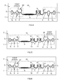
optical device 1 according to the invention are schematically illustrated inFigures 2 to 9 . As illustrated, such anoptical device 1 comprises asubstrate 2 and at least one primary waveguide 3j defined on thissubstrate 2. - Each primary waveguide 3j defines a loop reflector, that comprises first 41 and second 42 directional couplers, and a Mach-
Zehnder interferometer 5, that is intercalated (and integrated) between the first 41 and second 42 directional couplers and arranged for compensating a wavelength dependence of the directional couplers 4i (i = 1 or 2). - So, each primary waveguide 3j can be considered as a reflective wideband wavelength insensitive coupler (or RWINC), i.e. a new type of WINC working in a reflective mode.
- It is recalled that a WINC ("Wideband wavelength INsensitive Coupler") comprises two coupled waveguides defining together two directional couplers separated by a Mach-Zehnder configuration intended for compensating their wavelength dependence, but without providing any feedback into the same waveguide. Details of a WINC can be found in the document of Takagi, A; Jinguji, K.; Kawachi, M., "Silica-based waveguide-type wavelength-insensitive couplers (WINC's) with series-tapered coupling structure", IEEE Journal of Lightwave Technology, vol.10, n°12, pp.1814,1824, Dec 1992.
- So, each primary waveguide 3j (or RWINC) offers several degrees of freedom allowing to adjust its reflection/transmission coefficient and to obtain a flat response on more than 100 nm to 500 nm. These degrees of freedom follows from the respective designs of the first 41 and second 42 directional couplers and the Mach-Zehnder
interferometer 5. - For instance, each primary waveguide 3j may be a rib or strip waveguide that is defined onto a
silicon substrate 2, possibily with interposition of an intermediate dielectric layer of SiO2 material and possibly buried by a dielectric material. - It is recalled that a rib waveguide is a waveguide that is partially etched, and a strip waveguide is a completely etched waveguide, possibly buried by dielectric material.
- In the case where the rib or strip waveguide 3j is defined onto a
silicon substrate 2, it can be also made of silicon. For instance, this rib or strip waveguide 3j may have a full thickness (in its non-etched part) comprised between approximately 200 nm and approximately 500 nm, and an etched part with a local thickness comprised between approximately 50 nm and approximately 500 nm and with a width comprised between approximately 200 nm and approximately 800 nm. - Also for instance, the first
directional coupler 41 may have a length comprised between approximately 5 µm and approximately 200 µm, the seconddirectional coupler 42 may have a length comprised between approximately 5 µm and approximately 200 µm, and the Mach-Zehnderinterferometer 5 may have a length comprised between approximately 0.1 µm and approximately 2 µm. - The intervals of values given in the two last paragraphs contain values allowing to control the power reflection/transmission of each primary waveguide 3j in combination with its shape.
- As an example, for obtaining an input power reflection equal to 20%, the full thickness of the rib waveguide may be approximately equal to 300 nm, the rib local (or intermediate) thickness may be approximately equal to 150 nm, the rib width may be approximately equal to 550 nm, the first directional coupler length may be approximately equal to 13.29 µm, the second directional coupler length may be approximately equal to 7.35 µm, and the Mach-Zehnder interferometer length may be approximately equal to 0.267 µm.
- The values given in the last paragraph allow a working at a center wavelength of 1.3 µm on a wavelength window covering approximately 200 nm from approximately 1200 nm to approximately 1400 nm, with transmission and reflection power variations remaining under 0.1 dB.
- It is important to note that the RWINC 3j is robust against the fabrication variations. Indeed, when the waveguide width is increased by 10 nm (for instance from 550 nm to 560 nm), while keeping the other parameters constant, the reflection and transmission coefficients remain within 0.1 dB.
- As illustrated in
Figure 2 to 9 , one or more primary waveguides 32 may be combined with one or more other integrated optical elements or components. - In the non-limiting first example illustrated in
Figure 2 , theoptical device 1 comprises a first primary waveguides 31 defining a RWINC and having an input end and an output end. - In the non-limiting second and third examples illustrated in
Figures 3 and4 , theoptical device 1 comprises first 31 and second 32 primary waveguides defining two RWINCs, asecondary waveguide 6, aring resonator 7 and a heating means 8 in order to define ahybrid laser 18 or 18' with a broadband and controlled feedback provided by the two RWINCs 3j. Each primary waveguide 3j has an input/output end. Thesecondary waveguide 6 comprises a gain section, for instance made of Indium Phosphide (or InP), and intercalated between first and second ends. The first end of thesecondary waveguide 6 is connected to the input/output end of the first primary waveguide 31. Thering resonator 7 is intercalated between the second end of thesecondary waveguide 6 and the input/output end of the second primary waveguide 32. The heating means 8 is defined over thering resonator 7 and is arranged for controlling the filter peak wavelength of thering resonator 7 and for selecting a laser optical mode. - In the non-limiting example illustrated in
Figure 3 , the first primary waveguide 31 is a reflector with a reflection coefficient comprised between approximately 80% and approximately 100%, while the second primary waveguide 32 is an other reflector with a reflection coefficient comprised between approximately 10% and approximately 60% and that comprises anoutput 20 for delivering photons generated by thehybrid laser 18. For instance, the reflection coefficient of the second primary waveguide 32 may be equal to 30%. - In the non-limiting example illustrated in
Figure 4 , the second primary waveguide 32 is a reflector with a reflection coefficient comprised between approximately 80% and approximately 100%, while the first primary waveguide 31 is an other reflector with a reflection coefficient comprised between approximately 10% and approximately 60% and that comprises an output 20' for delivering photons generated by the hybrid laser 18'. For instance, the reflection coefficient of the first primary waveguide 31 may be equal to 30%. - In the non-limiting examples illustrated in
Figure 3 and4 , the laser cavity includes one gain section and one ring resonator (RR) acting as a filter for single mode selection. In the configuration ofFigure 3 , the RWINC partial reflector for the output is located after the ring resonator RR. In the configuration ofFigure 4 , the RWINC partial reflector for the output is located after the gain section. In the configuration ofFigure 3 , the side mode suppression ratio (SMSR) is expected to be better than in the configuration ofFigure 4 , but the output power is expected to be lower. - In the non-limiting fourth and fifth examples illustrated in
Figures 5 and 6 , theoptical device 1 comprises first 31 and second 32 primary waveguides defining two RWINCs, asecondary waveguide 6, anintermediate waveguide 9, afirst ring resonator 10 acting as a filter, asecond ring resonator 11 acting as a filter, and first 12 and second 12' heating means to respectively tune the first 10 and second 11 ring resonators in order to define another hybrid laser 19 or 19' with a broadband and controlled feedback provided by the two RWINCs 3j. Each primary waveguide 3j has an input/output end. Thesecondary waveguide 6 comprises a gain section, for instance made of Indium Phosphide (or InP), and intercalated between first and second ends. The first end of thesecondary waveguide 6 is connected to the input/output end of the first primary waveguide 31. Theintermediate waveguide 9 comprises first and second ends. Thefirst ring resonator 10 is intercalated between the second end of thesecondary waveguide 6 and the first end of theintermediate waveguide 9 for coupling thissecondary waveguide 6 to thisintermediate waveguide 9. The heating means 12 is defined over thefirst ring resonator 10 and is arranged for controlling the peak wavelength of thisfirst ring resonator 10. Thesecond ring resonator 11 is intercalated between the second end of theintermediate waveguide 9 and the input/output end of the second primary waveguide 32. The heating means 12' is defined over thesecond ring resonator 11 and is arranged for controlling the peak wavelength of thissecond ring resonator 11. Coordinated tuning of both first 10 and second 11 ring resonators filters allow for single mode selection and laser wavelength tuning. - The use of first 10 and second 11 ring resonators filters can allow for a larger tuning range and a better side mode suppression ratio (SMSR) for the laser. Usually, the first 10 and second 11 ring resonators have a slightly different Free Spectral Range (FSR) resulting in a composite filter with very large FSR. Vernier effect is being used to obtain large tuning ranges. Hyrbid laser making use of this filtering technique to obtain a wide tuning range are described in Le Liepvre, A.; Jany, C.; Accard, A.; Lamponi, M.; Poingt, F.; Make, D.; Lelarge, F.; Fedeli, J.-M.; Messaoudene, S.; Bordel, D.; Duan, G.-H., "Widely wavelength tunable hybrid III-V/silicon laser with 45 nm tuning range fabricated using a wafer bonding technique", Group IV Photonics (GFP), 2012 IEEE 9th International Conference, pp.54,56, 29-31 Aug. 2012.
- In the non-limiting example illustrated in
Figure 5 , the first primary waveguide 31 is a reflector with a reflection coefficient approximately equal to 100%, while the second primary waveguide 32 is an other reflector with a reflection coefficient comprised between approximately 10% and approximately 60% and that comprises anoutput 20 for delivering photons generated by thehybrid laser 19. For instance, the reflection coefficient of the second primary waveguide 32 may be equal to 30%. - In the non-limiting example illustrated in
Figure 6 , the second primary waveguide 32 is a reflector with a reflection coefficient approximately equal to 100%, while the first primary waveguide 31 is an other reflector with a reflection coefficient comprised between approximately 10% and approximately 60% and that comprises an output 20' for delivering photons generated by the hybrid laser 19'. For instance, the reflection coefficient of the first primary waveguide 31 may be equal to 30%. - In the non-limiting sixth and seventh examples illustrated in
Figures 7 and 8 , theoptical device 1 comprises ahybrid laser Figures 3 to 6 ) combined with an integrated element that may be chosen from a group comprising a semiconductor optical amplifier (or SOA) 21, a silicon photonic modulator (or SPM) 21 or a semiconductor electroabsorbtion modulator (EAM) 21, and a silicon photoniccoherent mixer 22 coupled tobalanced photodiodes 23, for instance. Each integrated element comprises an end connected to an output end delivering photons and belonging to one of the first 31 and second 32 primary waveguides of thehybrid laser - The use of RWINCs 3j in a tunable laser allows a robustness of fabrication, broadband performances in low loss and flat response, and a controlled reflectivity.
- In the non-limiting eighth example illustrated in
Figure 9 , theoptical device 1 comprises at least two primary waveguides 3j combined with a reflective arrayed waveguide grating (or R-AWG) 24 or an echelle grating. The use of flat reflectors (RWINCs) 3j allows large wavelength windows. - The reflective arrayed waveguide grating 24 or echelle grating comprises at least one input connected to an
input waveguide 25 defined on thesubstrate 1, at least two outputs connected respectively tooutput waveguides 26 defined on thesubstrate 1, and at least two inputs/outputs connected respectively to output ends of the primary waveguides 3j viawaveguides 27 defined on thesubstrate 1. In the non-limiting example illustrated inFigure 9 , the reflective arrayed waveguide grating 24 comprises one input connected to aninput waveguide 25, four outputs connected respectively to fouroutput waveguides 26, and seven inputs/outputs connected respectively to output ends of seven primary waveguides 3j via sevenwaveguides 27. But the respective numbers of inputs, outputs and inputs/outputs of the reflective arrayed waveguide grating 24 could be different from the ones illustrated inFigure 9 . - The invention offers several advantages, amongst which:
- the integration of reflectors with other integrated optical elements (or components), which is not the case when the reflector comprises cleaved facets,
- an extended wavelength window compare to the one offered by a loop reflector,
- an extended wavelength window and lower losses compare to the ones offered by a bragg reflector.
- It should be appreciated by those skilled in the art that any block diagram herein represent conceptual views of illustrative circuitry embodying the principles of the invention.
- The description and drawings merely illustrate the principles of the invention. It will thus be appreciated that those skilled in the art will be able to devise various arrangements that, although not explicitly described or shown herein, embody the principles of the invention and are included within its spirit and scope. Furthermore, all examples recited herein are principally intended expressly to be only for pedagogical purposes to aid the reader in understanding the principles of the invention and the concepts contributed by the inventor(s) to furthering the art, and are to be construed as being without limitation to such specifically recited examples and conditions. Moreover, all statements herein reciting principles, aspects, and embodiments of the invention, as well as specific examples thereof, are intended to encompass equivalents thereof.
Claims (11)
- Optical device (1) comprising a substrate (2) on which is defined at least one primary waveguide (3j) defining a loop reflector, comprising first (41) and second (42) directional couplers, and a Mach-Zehnder interferometer (5) intercalated between said first (41) and second (42) directional couplers and arranged for compensating a wavelength dependence of said directional couplers (4i).
- Optical device according to claim 1, wherein said primary waveguide (3j) is a rib or strip waveguide defined onto a silicon substrate (2).
- Optical device according to claim 2, wherein said rib or strip waveguide is made of silicon.
- Optical device according to claim 3, wherein said rib waveguide has a full thickness comprised between approximately 200 nm and approximately 500 nm, and an etched part with a local thickness comprised between approximately 50 nm and approximately 500 nm and with a width comprised between approximately 200 nm and approximately 800 nm.
- Optical device according to one of claims 3 and 4, wherein said first directional coupler (41) has a length comprised between approximately 5 µm and approximately 200 µm, said second directional coupler (42) has a length comprised between approximately 5 µm and approximately 200 µm, and said Mach-Zehnder interferometer (5) has a length comprised between approximately 0.1 µm and approximately 2 µm.
- Optical device according to one of claims 1 to 5, wherein it comprises first (31) and second (32) primary waveguides, each having an input/output end, a secondary waveguide (6) comprising a gain section intercalated between a first end, connected to the input/output end of said first primary waveguide (31), and a second end, a ring resonator (7) intercalated between the second end of said secondary waveguide (6) and the input/output end of said second primary waveguide (32), and a heating means (8) defined over said ring resonator (7) and arranged for controlling a filter peak wavelength of said ring resonator (7) and for selecting a laser optical mode.
- Optical device according to one of claims 1 to 5, wherein it comprises first (31) and second (32) primary waveguides, each having an input/output end, a secondary waveguide (6) comprising a gain section intercalated between a first end, connected to the input/output end of said first primary waveguide (31), and a second end, an intermediate waveguide (9) comprising first and second ends, a first ring resonator (10) with a wavelength spectral filtering and intercalated between the second end of said secondary waveguide (6) and the first end of said intermediate waveguide (9) for coupling said secondary waveguide (6) to said intermediate waveguide (9), a first heating means (12) defined over said first ring resonator (10) and arranged for controlling a filter peak wavelength of said first ring resonator (10), a second ring resonator (11) with a wavelength spectral filtering and intercalated between the second end of said intermediate waveguide (9) and the input/output end of said second primary waveguide (32), and a second heating means (12') defined over said second ring resonator (11) and arranged for controlling a filter peak wavelength of said second ring resonator (11).
- Optical device according to one of claims 6 and 7, wherein said first primary waveguide (31) is a reflector with a reflection coefficient comprised between approximately 80% and approximately 100%, and said second primary waveguide (32) is a reflector with a reflection coefficient comprised between approximately 10% and approximately 60% and comprising an output for delivering photons.
- Optical device according to one of claims 6 and 7, wherein said second primary waveguide (32) is a reflector with a reflection coefficient comprised between approximately 80% and approximately 100%, and said first primary waveguide (31) is a reflector with a reflection coefficient comprised between approximately 10% and approximately 60% and comprising an output for delivering photons.
- Optical device according to one of claims 6 to 9, wherein it further comprises an integrated element chosen from a group comprising a semiconductor optical amplifier, a semiconductor electroabsorption modulator, a silicon photonic modulator, a silicon photonic coherent mixer coupled to balanced photodiodes, and comprising an end connected to an output end of one of said first (31) and second (32) primary waveguides that is intended for delivering photons.
- Optical device according to one of claims 1 to 5, wherein it comprises at least two primary waveguides (3j) and a reflective arrayed waveguide grating (24) or an echelle grating comprising at least one input connected to an input waveguide (25), at least two outputs connected respectively to output waveguides (26) and at least two inputs/outputs connected respectively to output ends of said primary waveguides (3j) via waveguides (27).
Priority Applications (2)
| Application Number | Priority Date | Filing Date | Title |
|---|---|---|---|
| EP14307007.6A EP3032303B1 (en) | 2014-12-11 | 2014-12-11 | Optical device with integrated reflector(s) comprising a loop reflector integrating a mach-zehnder interferometer |
| US14/964,092 US9927676B2 (en) | 2014-12-11 | 2015-12-09 | Optical device with integrated reflector(s) comprising a loop reflector integrating a mach-zehnder interferometer |
Applications Claiming Priority (1)
| Application Number | Priority Date | Filing Date | Title |
|---|---|---|---|
| EP14307007.6A EP3032303B1 (en) | 2014-12-11 | 2014-12-11 | Optical device with integrated reflector(s) comprising a loop reflector integrating a mach-zehnder interferometer |
Publications (2)
| Publication Number | Publication Date |
|---|---|
| EP3032303A1 true EP3032303A1 (en) | 2016-06-15 |
| EP3032303B1 EP3032303B1 (en) | 2020-06-10 |
Family
ID=52272991
Family Applications (1)
| Application Number | Title | Priority Date | Filing Date |
|---|---|---|---|
| EP14307007.6A Active EP3032303B1 (en) | 2014-12-11 | 2014-12-11 | Optical device with integrated reflector(s) comprising a loop reflector integrating a mach-zehnder interferometer |
Country Status (2)
| Country | Link |
|---|---|
| US (1) | US9927676B2 (en) |
| EP (1) | EP3032303B1 (en) |
Cited By (1)
| Publication number | Priority date | Publication date | Assignee | Title |
|---|---|---|---|---|
| CN106932862A (en) * | 2017-04-20 | 2017-07-07 | 上海交通大学 | Coarse Wave Division Multiplexer based on silicon-based nano beam loop structure |
Families Citing this family (4)
| Publication number | Priority date | Publication date | Assignee | Title |
|---|---|---|---|---|
| US10551714B2 (en) * | 2017-05-17 | 2020-02-04 | Finisar Sweden Ab | Optical device |
| FR3088776B1 (en) * | 2018-11-15 | 2020-11-20 | Commissariat Energie Atomique | SEMICONDUCTOR LASER SOURCE |
| FR3107400B1 (en) * | 2020-02-19 | 2022-02-04 | Commissariat Energie Atomique | Tunable Vernier effect laser emission device |
| JP7254259B1 (en) * | 2022-07-04 | 2023-04-07 | 三菱電機株式会社 | multimode laser |
Citations (4)
| Publication number | Priority date | Publication date | Assignee | Title |
|---|---|---|---|---|
| US5453836A (en) * | 1993-04-22 | 1995-09-26 | Agency For Defense Development | Fiber optic laser rotation sensor utilizing a fiber loop reflector |
| US5892869A (en) * | 1996-06-24 | 1999-04-06 | Trw Inc. | Optical-loop signal processing using reflection mechanisms |
| EP1024378A2 (en) * | 1999-01-27 | 2000-08-02 | Lucent Technologies Inc. | Optical channel selector |
| US20030202743A1 (en) * | 2002-04-24 | 2003-10-30 | Fujitsu Limited | Wavelength dispersion compensating filter |
Family Cites Families (3)
| Publication number | Priority date | Publication date | Assignee | Title |
|---|---|---|---|---|
| JP2003337236A (en) * | 2002-05-17 | 2003-11-28 | Nec Corp | Optical ring resonator, optical waveguide device and method of manufacturing optical ring resonator |
| EP1420284A1 (en) * | 2002-11-14 | 2004-05-19 | Avanex Corporation | Birefringence trimming of integrated optical devices by elevated heating |
| WO2010138849A1 (en) * | 2009-05-29 | 2010-12-02 | Massachusetts Institute Of Technology | Cavity dynamics compensation in resonant optical modulators |
-
2014
- 2014-12-11 EP EP14307007.6A patent/EP3032303B1/en active Active
-
2015
- 2015-12-09 US US14/964,092 patent/US9927676B2/en active Active
Patent Citations (4)
| Publication number | Priority date | Publication date | Assignee | Title |
|---|---|---|---|---|
| US5453836A (en) * | 1993-04-22 | 1995-09-26 | Agency For Defense Development | Fiber optic laser rotation sensor utilizing a fiber loop reflector |
| US5892869A (en) * | 1996-06-24 | 1999-04-06 | Trw Inc. | Optical-loop signal processing using reflection mechanisms |
| EP1024378A2 (en) * | 1999-01-27 | 2000-08-02 | Lucent Technologies Inc. | Optical channel selector |
| US20030202743A1 (en) * | 2002-04-24 | 2003-10-30 | Fujitsu Limited | Wavelength dispersion compensating filter |
Non-Patent Citations (4)
| Title |
|---|
| LE LIEPVRE, A.; JANY, C.; ACCARD, A.; LAMPONI, M.; POINGT, F.; MAKE, D.; LELARGE, F.; FEDELI, J.-M.; MESSAOUDENE, S.; BORDEL, D.: "Widely wavelength tunable hybrid III-V/silicon laser with 45 nm tuning range fabricated using a wafer bonding technique", GROUP IV PHOTONICS (GFP), 2012 IEEE 9TH INTERNATIONAL CONFERENCE, 22 August 2012 (2012-08-22), pages 54,56 |
| LENZ G ET AL: "General Optical All-Pass Filter Structures for Dispersion Control in WDM Systems", JOURNAL OF LIGHTWAVE TECHNOLOGY, IEEE SERVICE CENTER, NEW YORK, NY, US, vol. 17, no. 7, 1 July 1999 (1999-07-01), XP011029460, ISSN: 0733-8724 * |
| MADSEN C K ET AL: "Integrated all-pass filters for tunable dispersion and dispersion slope compensation", IEEE PHOTONICS TECHNOLOGY LETTERS, IEEE SERVICE CENTER, PISCATAWAY, NJ, US, vol. 11, no. 12, 1 December 1999 (1999-12-01), pages 1623 - 1625, XP011426069, ISSN: 1041-1135, DOI: 10.1109/68.806867 * |
| TAKAGI, A; JINGUJI, K.; KAWACHI, M.: "Silica-based waveguide-type wavelength-insensitive couplers (WINC's) with series-tapered coupling structure", IEEE JOURNAL OF LIGHTWAVE TECHNOLOGY, vol. 10, no. 12, December 1992 (1992-12-01), pages 1814,1824, XP000367885, DOI: doi:10.1109/50.202833 |
Cited By (2)
| Publication number | Priority date | Publication date | Assignee | Title |
|---|---|---|---|---|
| CN106932862A (en) * | 2017-04-20 | 2017-07-07 | 上海交通大学 | Coarse Wave Division Multiplexer based on silicon-based nano beam loop structure |
| CN106932862B (en) * | 2017-04-20 | 2019-05-28 | 上海交通大学 | Coarse Wave Division Multiplexer based on silicon-based nano beam loop structure |
Also Published As
| Publication number | Publication date |
|---|---|
| US20160170286A1 (en) | 2016-06-16 |
| EP3032303B1 (en) | 2020-06-10 |
| US9927676B2 (en) | 2018-03-27 |
Similar Documents
| Publication | Publication Date | Title |
|---|---|---|
| US10355448B2 (en) | Tunable laser source | |
| JP5458194B2 (en) | Semiconductor tunable laser | |
| JP5692387B2 (en) | Semiconductor optical device | |
| US9130350B2 (en) | Laser device that includes ring resonator | |
| US8615025B2 (en) | Method and system for hybrid integration of a tunable laser | |
| US9270078B2 (en) | Tunable SOI laser | |
| US9318868B2 (en) | Tunable hybrid laser with carrier-induced phase control | |
| Le Liepvre et al. | Widely wavelength tunable hybrid III–V/silicon laser with 45 nm tuning range fabricated using a wafer bonding technique | |
| US20170353001A1 (en) | Tunable laser | |
| JP4942429B2 (en) | Semiconductor tunable laser | |
| US9927676B2 (en) | Optical device with integrated reflector(s) comprising a loop reflector integrating a mach-zehnder interferometer | |
| US12368283B2 (en) | Broadband arbitrary wavelength multichannel laser source | |
| JP5357214B2 (en) | Optical integrated circuit | |
| WO2013145271A1 (en) | Optical element, light transmitting element, light receiving element, hybrid laser, and light transmitting apparatus | |
| KR20120070836A (en) | Multi-wavelength optical source generator | |
| JP6510391B2 (en) | Semiconductor laser | |
| US20200381896A1 (en) | Laser device | |
| CN113644543B (en) | Semiconductor laser with tunable wavelength | |
| JP2011142191A (en) | Semiconductor wavelength tunable laser | |
| US20210255394A1 (en) | Tunable vernier effect laser emission device | |
| JP2017187690A (en) | Optical element, optical module and optical transmission system | |
| JP5713378B2 (en) | Waveguide type optical filter and semiconductor laser | |
| JP4962279B2 (en) | Semiconductor device, semiconductor optical integrated device, and optical transmission device | |
| JP2006330104A (en) | Waveguide filter and semiconductor laser device using the same | |
| Yoon et al. | Monolithically integrated tunable laser using double-ring resonators with a tilted multimode interference coupler |
Legal Events
| Date | Code | Title | Description |
|---|---|---|---|
| PUAI | Public reference made under article 153(3) epc to a published international application that has entered the european phase |
Free format text: ORIGINAL CODE: 0009012 |
|
| AK | Designated contracting states |
Kind code of ref document: A1 Designated state(s): AL AT BE BG CH CY CZ DE DK EE ES FI FR GB GR HR HU IE IS IT LI LT LU LV MC MK MT NL NO PL PT RO RS SE SI SK SM TR |
|
| AX | Request for extension of the european patent |
Extension state: BA ME |
|
| STAA | Information on the status of an ep patent application or granted ep patent |
Free format text: STATUS: REQUEST FOR EXAMINATION WAS MADE |
|
| 17P | Request for examination filed |
Effective date: 20161122 |
|
| RBV | Designated contracting states (corrected) |
Designated state(s): AL AT BE BG CH CY CZ DE DK EE ES FI FR GB GR HR HU IE IS IT LI LT LU LV MC MK MT NL NO PL PT RO RS SE SI SK SM TR |
|
| RAP1 | Party data changed (applicant data changed or rights of an application transferred) |
Owner name: COMMISSARIAT A L'ENERGIE ATOMIQUE ET AUX ENERGIES Owner name: THALES Owner name: ALCATEL LUCENT |
|
| STAA | Information on the status of an ep patent application or granted ep patent |
Free format text: STATUS: EXAMINATION IS IN PROGRESS |
|
| 17Q | First examination report despatched |
Effective date: 20190523 |
|
| GRAP | Despatch of communication of intention to grant a patent |
Free format text: ORIGINAL CODE: EPIDOSNIGR1 |
|
| STAA | Information on the status of an ep patent application or granted ep patent |
Free format text: STATUS: GRANT OF PATENT IS INTENDED |
|
| RIC1 | Information provided on ipc code assigned before grant |
Ipc: G02B 6/12 20060101ALI20191204BHEP Ipc: G02B 6/293 20060101AFI20191204BHEP Ipc: H01S 5/14 20060101ALI20191204BHEP Ipc: G02F 1/225 20060101ALI20191204BHEP Ipc: G02F 1/01 20060101ALI20191204BHEP |
|
| INTG | Intention to grant announced |
Effective date: 20200108 |
|
| GRAS | Grant fee paid |
Free format text: ORIGINAL CODE: EPIDOSNIGR3 |
|
| GRAA | (expected) grant |
Free format text: ORIGINAL CODE: 0009210 |
|
| STAA | Information on the status of an ep patent application or granted ep patent |
Free format text: STATUS: THE PATENT HAS BEEN GRANTED |
|
| AK | Designated contracting states |
Kind code of ref document: B1 Designated state(s): AL AT BE BG CH CY CZ DE DK EE ES FI FR GB GR HR HU IE IS IT LI LT LU LV MC MK MT NL NO PL PT RO RS SE SI SK SM TR |
|
| REG | Reference to a national code |
Ref country code: GB Ref legal event code: FG4D |
|
| REG | Reference to a national code |
Ref country code: AT Ref legal event code: REF Ref document number: 1279641 Country of ref document: AT Kind code of ref document: T Effective date: 20200615 Ref country code: CH Ref legal event code: EP |
|
| REG | Reference to a national code |
Ref country code: DE Ref legal event code: R096 Ref document number: 602014066441 Country of ref document: DE |
|
| REG | Reference to a national code |
Ref country code: IE Ref legal event code: FG4D |
|
| REG | Reference to a national code |
Ref country code: CH Ref legal event code: NV Representative=s name: NOVAGRAAF INTERNATIONAL SA, CH |
|
| REG | Reference to a national code |
Ref country code: LT Ref legal event code: MG4D |
|
| PG25 | Lapsed in a contracting state [announced via postgrant information from national office to epo] |
Ref country code: FI Free format text: LAPSE BECAUSE OF FAILURE TO SUBMIT A TRANSLATION OF THE DESCRIPTION OR TO PAY THE FEE WITHIN THE PRESCRIBED TIME-LIMIT Effective date: 20200610 Ref country code: LT Free format text: LAPSE BECAUSE OF FAILURE TO SUBMIT A TRANSLATION OF THE DESCRIPTION OR TO PAY THE FEE WITHIN THE PRESCRIBED TIME-LIMIT Effective date: 20200610 Ref country code: NO Free format text: LAPSE BECAUSE OF FAILURE TO SUBMIT A TRANSLATION OF THE DESCRIPTION OR TO PAY THE FEE WITHIN THE PRESCRIBED TIME-LIMIT Effective date: 20200910 Ref country code: SE Free format text: LAPSE BECAUSE OF FAILURE TO SUBMIT A TRANSLATION OF THE DESCRIPTION OR TO PAY THE FEE WITHIN THE PRESCRIBED TIME-LIMIT Effective date: 20200610 Ref country code: GR Free format text: LAPSE BECAUSE OF FAILURE TO SUBMIT A TRANSLATION OF THE DESCRIPTION OR TO PAY THE FEE WITHIN THE PRESCRIBED TIME-LIMIT Effective date: 20200911 |
|
| REG | Reference to a national code |
Ref country code: NL Ref legal event code: MP Effective date: 20200610 |
|
| PG25 | Lapsed in a contracting state [announced via postgrant information from national office to epo] |
Ref country code: LV Free format text: LAPSE BECAUSE OF FAILURE TO SUBMIT A TRANSLATION OF THE DESCRIPTION OR TO PAY THE FEE WITHIN THE PRESCRIBED TIME-LIMIT Effective date: 20200610 Ref country code: RS Free format text: LAPSE BECAUSE OF FAILURE TO SUBMIT A TRANSLATION OF THE DESCRIPTION OR TO PAY THE FEE WITHIN THE PRESCRIBED TIME-LIMIT Effective date: 20200610 Ref country code: HR Free format text: LAPSE BECAUSE OF FAILURE TO SUBMIT A TRANSLATION OF THE DESCRIPTION OR TO PAY THE FEE WITHIN THE PRESCRIBED TIME-LIMIT Effective date: 20200610 Ref country code: BG Free format text: LAPSE BECAUSE OF FAILURE TO SUBMIT A TRANSLATION OF THE DESCRIPTION OR TO PAY THE FEE WITHIN THE PRESCRIBED TIME-LIMIT Effective date: 20200910 |
|
| REG | Reference to a national code |
Ref country code: AT Ref legal event code: MK05 Ref document number: 1279641 Country of ref document: AT Kind code of ref document: T Effective date: 20200610 |
|
| PG25 | Lapsed in a contracting state [announced via postgrant information from national office to epo] |
Ref country code: NL Free format text: LAPSE BECAUSE OF FAILURE TO SUBMIT A TRANSLATION OF THE DESCRIPTION OR TO PAY THE FEE WITHIN THE PRESCRIBED TIME-LIMIT Effective date: 20200610 Ref country code: AL Free format text: LAPSE BECAUSE OF FAILURE TO SUBMIT A TRANSLATION OF THE DESCRIPTION OR TO PAY THE FEE WITHIN THE PRESCRIBED TIME-LIMIT Effective date: 20200610 |
|
| PG25 | Lapsed in a contracting state [announced via postgrant information from national office to epo] |
Ref country code: PT Free format text: LAPSE BECAUSE OF FAILURE TO SUBMIT A TRANSLATION OF THE DESCRIPTION OR TO PAY THE FEE WITHIN THE PRESCRIBED TIME-LIMIT Effective date: 20201012 Ref country code: RO Free format text: LAPSE BECAUSE OF FAILURE TO SUBMIT A TRANSLATION OF THE DESCRIPTION OR TO PAY THE FEE WITHIN THE PRESCRIBED TIME-LIMIT Effective date: 20200610 Ref country code: CZ Free format text: LAPSE BECAUSE OF FAILURE TO SUBMIT A TRANSLATION OF THE DESCRIPTION OR TO PAY THE FEE WITHIN THE PRESCRIBED TIME-LIMIT Effective date: 20200610 Ref country code: ES Free format text: LAPSE BECAUSE OF FAILURE TO SUBMIT A TRANSLATION OF THE DESCRIPTION OR TO PAY THE FEE WITHIN THE PRESCRIBED TIME-LIMIT Effective date: 20200610 Ref country code: AT Free format text: LAPSE BECAUSE OF FAILURE TO SUBMIT A TRANSLATION OF THE DESCRIPTION OR TO PAY THE FEE WITHIN THE PRESCRIBED TIME-LIMIT Effective date: 20200610 Ref country code: SM Free format text: LAPSE BECAUSE OF FAILURE TO SUBMIT A TRANSLATION OF THE DESCRIPTION OR TO PAY THE FEE WITHIN THE PRESCRIBED TIME-LIMIT Effective date: 20200610 Ref country code: EE Free format text: LAPSE BECAUSE OF FAILURE TO SUBMIT A TRANSLATION OF THE DESCRIPTION OR TO PAY THE FEE WITHIN THE PRESCRIBED TIME-LIMIT Effective date: 20200610 |
|
| PG25 | Lapsed in a contracting state [announced via postgrant information from national office to epo] |
Ref country code: IS Free format text: LAPSE BECAUSE OF FAILURE TO SUBMIT A TRANSLATION OF THE DESCRIPTION OR TO PAY THE FEE WITHIN THE PRESCRIBED TIME-LIMIT Effective date: 20201010 Ref country code: SK Free format text: LAPSE BECAUSE OF FAILURE TO SUBMIT A TRANSLATION OF THE DESCRIPTION OR TO PAY THE FEE WITHIN THE PRESCRIBED TIME-LIMIT Effective date: 20200610 Ref country code: PL Free format text: LAPSE BECAUSE OF FAILURE TO SUBMIT A TRANSLATION OF THE DESCRIPTION OR TO PAY THE FEE WITHIN THE PRESCRIBED TIME-LIMIT Effective date: 20200610 |
|
| REG | Reference to a national code |
Ref country code: DE Ref legal event code: R097 Ref document number: 602014066441 Country of ref document: DE |
|
| PLBE | No opposition filed within time limit |
Free format text: ORIGINAL CODE: 0009261 |
|
| STAA | Information on the status of an ep patent application or granted ep patent |
Free format text: STATUS: NO OPPOSITION FILED WITHIN TIME LIMIT |
|
| PG25 | Lapsed in a contracting state [announced via postgrant information from national office to epo] |
Ref country code: DK Free format text: LAPSE BECAUSE OF FAILURE TO SUBMIT A TRANSLATION OF THE DESCRIPTION OR TO PAY THE FEE WITHIN THE PRESCRIBED TIME-LIMIT Effective date: 20200610 |
|
| 26N | No opposition filed |
Effective date: 20210311 |
|
| PG25 | Lapsed in a contracting state [announced via postgrant information from national office to epo] |
Ref country code: SI Free format text: LAPSE BECAUSE OF FAILURE TO SUBMIT A TRANSLATION OF THE DESCRIPTION OR TO PAY THE FEE WITHIN THE PRESCRIBED TIME-LIMIT Effective date: 20200610 |
|
| PG25 | Lapsed in a contracting state [announced via postgrant information from national office to epo] |
Ref country code: MC Free format text: LAPSE BECAUSE OF FAILURE TO SUBMIT A TRANSLATION OF THE DESCRIPTION OR TO PAY THE FEE WITHIN THE PRESCRIBED TIME-LIMIT Effective date: 20200610 |
|
| REG | Reference to a national code |
Ref country code: BE Ref legal event code: MM Effective date: 20201231 |
|
| PG25 | Lapsed in a contracting state [announced via postgrant information from national office to epo] |
Ref country code: LU Free format text: LAPSE BECAUSE OF NON-PAYMENT OF DUE FEES Effective date: 20201211 Ref country code: IE Free format text: LAPSE BECAUSE OF NON-PAYMENT OF DUE FEES Effective date: 20201211 |
|
| PG25 | Lapsed in a contracting state [announced via postgrant information from national office to epo] |
Ref country code: TR Free format text: LAPSE BECAUSE OF FAILURE TO SUBMIT A TRANSLATION OF THE DESCRIPTION OR TO PAY THE FEE WITHIN THE PRESCRIBED TIME-LIMIT Effective date: 20200610 Ref country code: MT Free format text: LAPSE BECAUSE OF FAILURE TO SUBMIT A TRANSLATION OF THE DESCRIPTION OR TO PAY THE FEE WITHIN THE PRESCRIBED TIME-LIMIT Effective date: 20200610 Ref country code: CY Free format text: LAPSE BECAUSE OF FAILURE TO SUBMIT A TRANSLATION OF THE DESCRIPTION OR TO PAY THE FEE WITHIN THE PRESCRIBED TIME-LIMIT Effective date: 20200610 |
|
| PG25 | Lapsed in a contracting state [announced via postgrant information from national office to epo] |
Ref country code: MK Free format text: LAPSE BECAUSE OF FAILURE TO SUBMIT A TRANSLATION OF THE DESCRIPTION OR TO PAY THE FEE WITHIN THE PRESCRIBED TIME-LIMIT Effective date: 20200610 |
|
| PG25 | Lapsed in a contracting state [announced via postgrant information from national office to epo] |
Ref country code: BE Free format text: LAPSE BECAUSE OF NON-PAYMENT OF DUE FEES Effective date: 20201231 |
|
| REG | Reference to a national code |
Ref country code: CH Ref legal event code: U11 Free format text: ST27 STATUS EVENT CODE: U-0-0-U10-U11 (AS PROVIDED BY THE NATIONAL OFFICE) Effective date: 20260101 |
|
| PGFP | Annual fee paid to national office [announced via postgrant information from national office to epo] |
Ref country code: GB Payment date: 20251229 Year of fee payment: 12 |
|
| PGFP | Annual fee paid to national office [announced via postgrant information from national office to epo] |
Ref country code: FR Payment date: 20251222 Year of fee payment: 12 |
|
| PGFP | Annual fee paid to national office [announced via postgrant information from national office to epo] |
Ref country code: DE Payment date: 20251222 Year of fee payment: 12 |
|
| PGFP | Annual fee paid to national office [announced via postgrant information from national office to epo] |
Ref country code: IT Payment date: 20251231 Year of fee payment: 12 |
|
| PGFP | Annual fee paid to national office [announced via postgrant information from national office to epo] |
Ref country code: CH Payment date: 20260101 Year of fee payment: 12 |