EP3032268A1 - An integrated circuit with an on chip hall sensor - Google Patents
An integrated circuit with an on chip hall sensor Download PDFInfo
- Publication number
- EP3032268A1 EP3032268A1 EP14196982.4A EP14196982A EP3032268A1 EP 3032268 A1 EP3032268 A1 EP 3032268A1 EP 14196982 A EP14196982 A EP 14196982A EP 3032268 A1 EP3032268 A1 EP 3032268A1
- Authority
- EP
- European Patent Office
- Prior art keywords
- integrated circuit
- chip
- inductor element
- chip inductor
- circuit according
- Prior art date
- Legal status (The legal status is an assumption and is not a legal conclusion. Google has not performed a legal analysis and makes no representation as to the accuracy of the status listed.)
- Granted
Links
Images
Classifications
-
- G—PHYSICS
- G01—MEASURING; TESTING
- G01R—MEASURING ELECTRIC VARIABLES; MEASURING MAGNETIC VARIABLES
- G01R33/00—Arrangements or instruments for measuring magnetic variables
- G01R33/02—Measuring direction or magnitude of magnetic fields or magnetic flux
- G01R33/06—Measuring direction or magnitude of magnetic fields or magnetic flux using galvano-magnetic devices
- G01R33/07—Hall effect devices
- G01R33/072—Constructional adaptation of the sensor to specific applications
-
- G—PHYSICS
- G01—MEASURING; TESTING
- G01R—MEASURING ELECTRIC VARIABLES; MEASURING MAGNETIC VARIABLES
- G01R33/00—Arrangements or instruments for measuring magnetic variables
- G01R33/0017—Means for compensating offset magnetic fields or the magnetic flux to be measured; Means for generating calibration magnetic fields
-
- G—PHYSICS
- G01—MEASURING; TESTING
- G01R—MEASURING ELECTRIC VARIABLES; MEASURING MAGNETIC VARIABLES
- G01R15/00—Details of measuring arrangements of the types provided for in groups G01R17/00 - G01R29/00, G01R33/00 - G01R33/26 or G01R35/00
- G01R15/14—Adaptations providing voltage or current isolation, e.g. for high-voltage or high-current networks
- G01R15/20—Adaptations providing voltage or current isolation, e.g. for high-voltage or high-current networks using galvano-magnetic devices, e.g. Hall-effect devices, i.e. measuring a magnetic field via the interaction between a current and a magnetic field, e.g. magneto resistive or Hall effect devices
- G01R15/202—Adaptations providing voltage or current isolation, e.g. for high-voltage or high-current networks using galvano-magnetic devices, e.g. Hall-effect devices, i.e. measuring a magnetic field via the interaction between a current and a magnetic field, e.g. magneto resistive or Hall effect devices using Hall-effect devices
-
- G—PHYSICS
- G01—MEASURING; TESTING
- G01R—MEASURING ELECTRIC VARIABLES; MEASURING MAGNETIC VARIABLES
- G01R19/00—Arrangements for measuring currents or voltages or for indicating presence or sign thereof
- G01R19/0092—Measuring current only
Definitions
- the invention relates to an integrated circuit comprising at least one on chip Hall sensor plate adapted to measure an external and an internal magnetic field.
- a Hall sensor chip can be used for measuring or sensing an external magnetic field.
- the measured magnetic field can be a constant or alternating magnetic field.
- a Hall sensor is a transducer element that can vary its output voltage in response to an applied magnetic field.
- the Hall Effect comprises the generation of a voltage difference across an electrical conductor, transverse to an electric current in the conductor and a magnetic field being perpendicular to the electrical current.
- a magnetic field is generated, wherein the strength of the magnetic field is linear dependent on the amplitude of the electrical current flowing through the wire as described in the Biot-Savart law.
- the Biot-Savart law describes the magnetic field generated by an electrical current. It relates the magnetic field to the magnitude, direction, length and proximity of the electrical current.
- the Hall voltage appearing at the electrodes of a Hall sensor is linear dependent on the magnetic field strength of the magnetic field applied to the Hall sensor.
- Conventional Hall sensor chips are used for measurement or sensing an external constant or alternating magnetic field.
- the distance between the Hall sensor and the magnetic field source such as a conductor or an inductance, and their orientation constant and by also keeping the electric current passed through the Hall sensor plate constant, the amplitude of the flowing electrical current forming the magnetic field source can be measured.
- the distance and orientation constant is often difficult or even impossible.
- Conventional Hall sensor chips do not allow to measure the amplitude of electrical currents directly.
- the invention provides according to a first aspect an integrated circuit comprising at least one on chip Hall sensor plate configured to measure an external magnetic field characterized by an on chip inductor element connected to two current sense pins of said integrated circuit, wherein the on chip inductor element is configured to generate an internal magnetic field sensed by said on chip Hall sensor plate to measure an applied electrical current flowing through said on chip inductor element via said current sense pins of said integrated circuit.
- the integrated circuit according to the present invention provides a current sensing functionality to the integrated circuit.
- the advantage of the integrated circuit according to the present invention is that the measurement of the applied electric current can be measured very precisely, since the distance between the chip conductor element and the on chip Hall sensor plate is very small and exactly defined by the internal structure of the integrated circuit.
- the on chip inductor element comprises a rectangular form.
- the on chip inductor element comprises a spiral form.
- the on chip inductor element and the Hall sensor plate are provided at different layers of the integrated circuit providing a predetermined distance between the on chip inductor element and the Hall sensor plate.
- an overcurrent protection circuit is connected in series with the at least one on chip inductor element.
- the overcurrent protection circuit comprises a current sensing element and a low resistance switch connected in series with the on chip inductor element.
- a voltage drop at the current sensing element is amplified by a voltage amplifier adapted to control the low resistance switch of the overcurrent protection circuit.
- the voltage amplifier switches the low resistance switch off to interrupt a current flow through said on chip inductor element.
- the threshold voltage comprises a predetermined fixed threshold voltage.
- the threshold voltage comprises an adjustable and/or programmable threshold voltage.
- the current sensing element of the overcurrent protection circuit comprises an integrated resistor.
- the on chip Hall sensor plate is implemented by a N-well cross structure placed in a p-type silicon substrate of the integrated circuit.
- the on chip Hall sensor plate comprises four highly doped n+ contact areas connected to an interconnection metal layer of said integrated circuit isolated by an isolating layer from the p-type silicon substrate of said integrated circuit.
- the on chip inductor element is formed by a metal planar coil on a passivation layer covering the on chip Hall sensor plate and the interconnection metal layer.
- the on chip inductor element is bonded to chip frame pads of the integrated circuit.
- the on chip inductor element is connected to an on chip metal interconnection layer by means of via contacts.
- the on chip Hall sensor plate is configured to generate a Hall voltage being linear dependent on the magnetic field strength of the magnetic field caused by the electrical current flowing through said on chip inductor element.
- the generated Hall voltage is processed to evaluate the electrical current flowing through the on chip inductor element of said integrated chip.
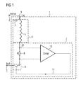
- Fig. 1 shows a circuit diagram of an exemplary embodiment of an integrated circuit 1 according to the present invention.
- the integrated circuit 1 comprises a first current sense pin 2 and a second current sense pin 3 which can be connected to an external electronic circuit for measuring an electric current flowing from the first current sense pin 2 through the integrated circuit 1 to the second current sense pin 3.
- the first current sense pin 2 is connected via an internal current line 4 to an integrated on chip inductor element 5 placed in the vicinity of an integrated on chip Hall sensor plate 6 of the integrated circuit 1.
- the on chip inductor element 5 and the Hall sensor plate 6 are provided at different layers of the integrated circuit 1. This implementation provides a predetermined distance between the on chip inductor element 5 and the Hall sensor plate 6.
- the Hall sensor plate 6 is located in another layer of the integrated chip beneath the on chip inductor element 5.
- the on chip inductor element 5 is an electric coil formed by an on chip inductor. This on chip inductor element 5 can be formed by a top or other metal layer of the integrated circuit 1.
- the coil or on chip inductor element 5 can comprise a rectangular or a spiral form and can have one or more turns in the same or different metal layers of the integrated circuit 1.
- the on chip inductor element 5 is configured to generate an internal magnetic field which is sensed by the on chip Hall sensor plate 6 for measuring the electric current I flowing through the on chip inductor element 5 via the current sense pins 2, 3 of the integrated circuit 1.
- the electric current I flowing through the on chip inductor element 5 generates a magnetic field B which is sensed directly by the Hall sensor plate 6 of the integrated circuit 1.
- the distance and the orientation of the on chip inductor element 5 creating the magnetic field and the Hall sensor plate 6 is kept always fixed. Because of the linear dependencies described above, after calibration, the electric current I passing through the on chip inductor element 5 can be directly converted in a linear dependent voltage at the output of the on chip Hall sensor plate 6.
- the Hall voltage generated by the on chip Hall sensor plate 6 can in a possible embodiment be directly applied to corresponding pins of the integrated circuit 1. In an alternative embodiment, the generated output voltage can be further processed internally by a processing unit of the integrated circuit 1.
- the on chip Hall sensor plate 6 is adapted to measure an external magnetic field caused by an electrical current flowing through another external wire located in the vicinity of the integrated chip 1. Accordingly, the on chip Hall sensor plate 6 is adapted to either measure an internal magnetic field B int caused by the on chip inductor element 5 or an external magnetic field B ext caused by an external coil or an external wire in the vicinity of the integrated chip 1.
- the integrated circuit 1 comprises an overcurrent protection circuit 7 connected in series with the at least one on chip inductor element 5.
- the overcurrent protection circuit 7 keeps the electric current flowing through the on chip inductor element 6 within safe limits. Because of the limitation of the current planar technologies caused by electric migration rules where the electric current I flowing through a conductive layer wire is limited by the width of the respective wire, the electric current passed through the on chip inductor element 6 is kept by the overcurrent protection circuit 7 within the required safe limits or ranges.
- the overcurrent protection circuit 7 comprises a current sensing element 8 and a low resistance switch 9 connected in series with the on chip inductor element 5.
- the current sensing element 8 can be formed by an integrated resistor as illustrated in Fig. 1 .
- a voltage drop at the current sensing element 8 is amplified by a voltage amplifier 10 of the overcurrent protection circuit 7 and the output of the voltage amplifier 10 is connected via a control signal line 11 to the low resistance switch 9 of the overcurrent protection circuit 7. If the voltage drop at the current sensing element 8 exceeds a threshold voltage V TH , the voltage amplifier 10 is adapted to switch the low resistance switch 9 of the overcurrent protection circuit 7 off to interrupt the electric current flowing through said on chip inductor element 5.
- the threshold voltage V TH can be a predetermined fixed threshold voltage. In an alternative embodiment, the threshold voltage V TH can be an adjustable and/or programmed threshold voltage.
- the overcurrent protection circuit 7 can in a possible embodiment be implemented in the same layer as the on chip inductor element 5 of the integrated circuit 1.
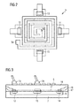
- Fig. 2 illustrates a possible exemplary embodiment of an on chip inductor element 5 used in the integrated circuit 1 according to the present invention.
- the on chip inductor element 5 comprises a spiral form.
- the spiral on chip inductor element 5 as shown in Fig. 2 comprises two connection terminals 5A, 5B, wherein the first connection 5A connects the on chip inductor element 5 with the current sense pin 2 of the integrated chip 1 via an internal current line 4 as illustrated in Fig. 1 .
- the other connection 5B of the on chip inductor element 5 connects the on chip inductor element 5 to the overcurrent protection circuit 7 as illustrated in Fig. 1 .
- the on chip Hall sensor plate 6 is located within another chip layer of the integrated circuit 1 as illustrated in the cross-section view of Fig. 3 .
- the on chip Hall sensor plate 6 can be implemented by a N-well cross structure placed in a p-type silicon substrate 7 of the integrated circuit 1.
- the on chip Hall sensor plate 6 can comprise four highly doped n+ contact areas 12, 13, 14, 15 as illustrated in Figs. 2, 3 . These highly doped n+ contact areas 12, 13, 14, 15 are connected in the illustrated embodiment to an interconnection metal layer 16 isolated by an isolation layer 17 from the p-type silicon substrate 7 of the integrated circuit.
- the isolating layer can be formed by a SiO 2 isolating layer.
- the Hall sensor plate 6 and the metal layer 16 are covered by a passivation layer 18 which can be formed by SiO 2 or Si 3 N 4 .
- the on chip inductor element 5 formed by the spiral coil 5 can be implemented as a metal planar coil in spiral form and placed on the passivation layer 18 as illustrated in Fig. 3 .
- the on chip inductor element 5 is bonded to chip frame pads of the integrated circuit 1.
- the on chip inductor element 5 is connected to an on chip metal interconnection layer by means of via contacts.
Landscapes
- Physics & Mathematics (AREA)
- Condensed Matter Physics & Semiconductors (AREA)
- General Physics & Mathematics (AREA)
- Semiconductor Integrated Circuits (AREA)
Abstract
Description
- The invention relates to an integrated circuit comprising at least one on chip Hall sensor plate adapted to measure an external and an internal magnetic field.
- A Hall sensor chip can be used for measuring or sensing an external magnetic field. The measured magnetic field can be a constant or alternating magnetic field. A Hall sensor is a transducer element that can vary its output voltage in response to an applied magnetic field. The Hall Effect comprises the generation of a voltage difference across an electrical conductor, transverse to an electric current in the conductor and a magnetic field being perpendicular to the electrical current.
- If a steady electrical current I passes through an electrical conductor wire of an inductance or coil, a magnetic field is generated, wherein the strength of the magnetic field is linear dependent on the amplitude of the electrical current flowing through the wire as described in the Biot-Savart law. The Biot-Savart law describes the magnetic field generated by an electrical current. It relates the magnetic field to the magnitude, direction, length and proximity of the electrical current. The Hall voltage appearing at the electrodes of a Hall sensor is linear dependent on the magnetic field strength of the magnetic field applied to the Hall sensor. The Hall voltage depends on the electric current I and the applied magnetic field B as follows:

where I is the electric current across the plate length of the Hall sensor plate, B is the applied magnetic field, t is the thickness of the Hall sensor plate, e is the elementary charge, and n is the charge carrier density of the carrier electrons. - Conventional Hall sensor chips are used for measurement or sensing an external constant or alternating magnetic field. By keeping the distance between the Hall sensor and the magnetic field source, such as a conductor or an inductance, and their orientation constant and by also keeping the electric current passed through the Hall sensor plate constant, the amplitude of the flowing electrical current forming the magnetic field source can be measured. However, keeping the distance and orientation constant is often difficult or even impossible. Conventional Hall sensor chips do not allow to measure the amplitude of electrical currents directly.
- Accordingly, it is an object of the present invention to provide an integrated circuit allowing to measure the amplitude of an electrical current directly.
- This object is achieved according to a first aspect of the present invention by an integrated circuit having the features of
claim 1. - The invention provides according to a first aspect an integrated circuit comprising at least one on chip Hall sensor plate configured to measure an external magnetic field characterized by an on chip inductor element connected to two current sense pins of said integrated circuit, wherein the on chip inductor element is configured to generate an internal magnetic field sensed by said on chip Hall sensor plate to measure an applied electrical current flowing through said on chip inductor element via said current sense pins of said integrated circuit.
- Accordingly, the integrated circuit according to the present invention provides a current sensing functionality to the integrated circuit.
- The advantage of the integrated circuit according to the present invention is that the measurement of the applied electric current can be measured very precisely, since the distance between the chip conductor element and the on chip Hall sensor plate is very small and exactly defined by the internal structure of the integrated circuit.
- In a possible embodiment of the integrated circuit according to the first aspect of the present invention, the on chip inductor element comprises a rectangular form.
- In a still further possible embodiment of the integrated circuit according to the first aspect of the present invention, the on chip inductor element comprises a spiral form.
- In a further possible embodiment of the integrated circuit according to the present invention, the on chip inductor element and the Hall sensor plate are provided at different layers of the integrated circuit providing a predetermined distance between the on chip inductor element and the Hall sensor plate.
- In a further possible embodiment of the integrated circuit according to the present invention, an overcurrent protection circuit is connected in series with the at least one on chip inductor element.
- In a further possible embodiment of the integrated circuit according to the present invention, the overcurrent protection circuit comprises a current sensing element and a low resistance switch connected in series with the on chip inductor element.
- In a further possible embodiment of the integrated circuit according to the present invention, a voltage drop at the current sensing element is amplified by a voltage amplifier adapted to control the low resistance switch of the overcurrent protection circuit.
- In a further possible embodiment of the integrated circuit according to the present invention, wherein if the voltage drop at the current sensing element exceeds a threshold voltage, the voltage amplifier switches the low resistance switch off to interrupt a current flow through said on chip inductor element.
- In a further possible embodiment of the integrated circuit according to the present invention, the threshold voltage comprises a predetermined fixed threshold voltage.
- In a further possible embodiment of the integrated circuit according to the present invention, the threshold voltage comprises an adjustable and/or programmable threshold voltage.
- In a further possible embodiment of the integrated circuit according to the present invention, the current sensing element of the overcurrent protection circuit comprises an integrated resistor.
- In a further possible embodiment of the integrated circuit according to the present invention, the on chip Hall sensor plate is implemented by a N-well cross structure placed in a p-type silicon substrate of the integrated circuit.
- In a further possible embodiment of the integrated circuit according to the present invention, the on chip Hall sensor plate comprises four highly doped n+ contact areas connected to an interconnection metal layer of said integrated circuit isolated by an isolating layer from the p-type silicon substrate of said integrated circuit.
- In a further possible embodiment of the integrated circuit according to the present invention, the on chip inductor element is formed by a metal planar coil on a passivation layer covering the on chip Hall sensor plate and the interconnection metal layer.
- In a further possible embodiment of the integrated circuit according to the present invention, the on chip inductor element is bonded to chip frame pads of the integrated circuit. In a further possible alternative embodiment of the integrated circuit, the on chip inductor element is connected to an on chip metal interconnection layer by means of via contacts.
- In a still further possible embodiment of the integrated circuit according to the present invention, the on chip Hall sensor plate is configured to generate a Hall voltage being linear dependent on the magnetic field strength of the magnetic field caused by the electrical current flowing through said on chip inductor element.
- In a further possible embodiment of the integrated circuit according to the present invention, the generated Hall voltage is processed to evaluate the electrical current flowing through the on chip inductor element of said integrated chip.
- In the following, possible embodiments of the integrated circuit are described in more detail with reference to the enclosed figures.
- Fig. 1
- shows a circuit diagram for illustrating a possible exemplary embodiment of an integrated circuit according to the present invention;
- Fig. 2
- shows a top view on a possible embodiment of an on chip inductor element as used by the integrated circuit according to the present invention;
- Fig. 3
- shows a cross-section view through an exemplary embodiment of an integrated circuit according to the present invention comprising an on chip inductor element as illustrated in
Fig. 2 . -
Fig. 1 shows a circuit diagram of an exemplary embodiment of an integratedcircuit 1 according to the present invention. Theintegrated circuit 1 comprises a firstcurrent sense pin 2 and a second current sense pin 3 which can be connected to an external electronic circuit for measuring an electric current flowing from the firstcurrent sense pin 2 through the integratedcircuit 1 to the second current sense pin 3. In the embodiment shown inFig. 1 , the firstcurrent sense pin 2 is connected via an internal current line 4 to an integrated onchip inductor element 5 placed in the vicinity of an integrated on chipHall sensor plate 6 of theintegrated circuit 1. In a possible embodiment, the onchip inductor element 5 and theHall sensor plate 6 are provided at different layers of the integratedcircuit 1. This implementation provides a predetermined distance between the onchip inductor element 5 and theHall sensor plate 6. In a possible embodiment, theHall sensor plate 6 is located in another layer of the integrated chip beneath the onchip inductor element 5. The onchip inductor element 5 is an electric coil formed by an on chip inductor. This onchip inductor element 5 can be formed by a top or other metal layer of the integratedcircuit 1. The coil or onchip inductor element 5 can comprise a rectangular or a spiral form and can have one or more turns in the same or different metal layers of the integratedcircuit 1. The onchip inductor element 5 is configured to generate an internal magnetic field which is sensed by the on chipHall sensor plate 6 for measuring the electric current I flowing through the onchip inductor element 5 via thecurrent sense pins 2, 3 of the integratedcircuit 1. The electric current I flowing through the onchip inductor element 5 generates a magnetic field B which is sensed directly by theHall sensor plate 6 of theintegrated circuit 1. The distance and the orientation of the onchip inductor element 5 creating the magnetic field and theHall sensor plate 6 is kept always fixed. Because of the linear dependencies described above, after calibration, the electric current I passing through the onchip inductor element 5 can be directly converted in a linear dependent voltage at the output of the on chipHall sensor plate 6. The Hall voltage generated by the on chipHall sensor plate 6 can in a possible embodiment be directly applied to corresponding pins of the integratedcircuit 1. In an alternative embodiment, the generated output voltage can be further processed internally by a processing unit of the integratedcircuit 1. If no electric current I passes through the onchip inductor element 5, the on chipHall sensor plate 6 is adapted to measure an external magnetic field caused by an electrical current flowing through another external wire located in the vicinity of the integratedchip 1. Accordingly, the on chipHall sensor plate 6 is adapted to either measure an internal magnetic field Bint caused by the onchip inductor element 5 or an external magnetic field Bext caused by an external coil or an external wire in the vicinity of theintegrated chip 1. - In the embodiment illustrated in
Fig. 1 , theintegrated circuit 1 comprises anovercurrent protection circuit 7 connected in series with the at least one onchip inductor element 5. Theovercurrent protection circuit 7 keeps the electric current flowing through the onchip inductor element 6 within safe limits. Because of the limitation of the current planar technologies caused by electric migration rules where the electric current I flowing through a conductive layer wire is limited by the width of the respective wire, the electric current passed through the onchip inductor element 6 is kept by theovercurrent protection circuit 7 within the required safe limits or ranges. In the embodiment shown inFig. 1 , theovercurrent protection circuit 7 comprises acurrent sensing element 8 and alow resistance switch 9 connected in series with the onchip inductor element 5. Thecurrent sensing element 8 can be formed by an integrated resistor as illustrated inFig. 1 . A voltage drop at thecurrent sensing element 8 is amplified by avoltage amplifier 10 of theovercurrent protection circuit 7 and the output of thevoltage amplifier 10 is connected via acontrol signal line 11 to thelow resistance switch 9 of theovercurrent protection circuit 7. If the voltage drop at thecurrent sensing element 8 exceeds a threshold voltage VTH, thevoltage amplifier 10 is adapted to switch thelow resistance switch 9 of theovercurrent protection circuit 7 off to interrupt the electric current flowing through said onchip inductor element 5. In a possible embodiment, the threshold voltage VTH can be a predetermined fixed threshold voltage. In an alternative embodiment, the threshold voltage VTH can be an adjustable and/or programmed threshold voltage. Theovercurrent protection circuit 7 can in a possible embodiment be implemented in the same layer as the onchip inductor element 5 of theintegrated circuit 1. -
Fig. 2 illustrates a possible exemplary embodiment of an onchip inductor element 5 used in theintegrated circuit 1 according to the present invention. In the embodiment shown inFig. 1 , the onchip inductor element 5 comprises a spiral form. The spiral onchip inductor element 5 as shown inFig. 2 comprises two connection terminals 5A, 5B, wherein the first connection 5A connects the onchip inductor element 5 with thecurrent sense pin 2 of theintegrated chip 1 via an internal current line 4 as illustrated inFig. 1 . The other connection 5B of the onchip inductor element 5 connects the onchip inductor element 5 to theovercurrent protection circuit 7 as illustrated inFig. 1 . Beneath the onchip inductor element 5, the on chipHall sensor plate 6 is located within another chip layer of theintegrated circuit 1 as illustrated in the cross-section view ofFig. 3 . As can be seen inFig. 3 , the on chipHall sensor plate 6 can be implemented by a N-well cross structure placed in a p-type silicon substrate 7 of theintegrated circuit 1. In a possible embodiment, the on chipHall sensor plate 6 can comprise four highly dopedn+ contact areas Figs. 2, 3 . These highly dopedn+ contact areas interconnection metal layer 16 isolated by anisolation layer 17 from the p-type silicon substrate 7 of the integrated circuit. In a possible embodiment, the isolating layer can be formed by a SiO2 isolating layer. TheHall sensor plate 6 and themetal layer 16 are covered by apassivation layer 18 which can be formed by SiO2 or Si3N4. The onchip inductor element 5 formed by thespiral coil 5 can be implemented as a metal planar coil in spiral form and placed on thepassivation layer 18 as illustrated inFig. 3 . In a possible embodiment, the onchip inductor element 5 is bonded to chip frame pads of theintegrated circuit 1. In a further possible alternative embodiment, the onchip inductor element 5 is connected to an on chip metal interconnection layer by means of via contacts.
Claims (15)
- An integrated circuit (1) comprising at least one on chip Hall sensor plate (6) configured to measure an external magnetic field
characterized by
an on chip inductor element (5) connected to two current sense pins (2, 3) of said integrated circuit (1), wherein the on chip inductor element (5) is configured to generate an internal magnetic field sensed by said on chip Hall sensor plate (6) to measure an applied electrical current (I) flowing through said on chip inductor element (5) via said current sense pins (2, 3) of said integrated circuit (1). - The integrated circuit according to claim 1, wherein the on chip inductor element (5) comprises a rectangular or spiral form.
- The integrated circuit according to claim 1 or 2, wherein the on chip inductor element (5) and the Hall sensor plate (6) are provided at different layers of the integrated circuit (1) providing a predetermined distance between the on chip inductor element (5) and the Hall sensor plate (6).
- The integrated circuit according to one of the preceding claims 1 to 3, wherein an overcurrent protection circuit (7) is connected in series with the at least one on chip inductor element (5).
- The integrated circuit according to claim 4, wherein the overcurrent protection circuit (7) comprises a current sensing element (8) and a low resistance switch (9) connected in series with the on chip inductor element (5).
- The integrated circuit according to claim 5, wherein a voltage drop at the current sensing element (8) is amplified by a voltage amplifier (10) adapted to control the low resistance switch (9) of the overcurrent protection circuit (7).
- The integrated circuit according to claim 6, wherein if the voltage drop at the current sensing element (8) exceeds a threshold voltage, the voltage amplifier (10) switches the low resistance switch (9) off to interrupt a current flow through said on chip inductor element (5).
- The integrated circuit according to claim 7, wherein the threshold voltage comprises a predetermined threshold voltage or an adjustable and/or programmed threshold voltage.
- The integrated circuit according to one of the preceding claims 6 to 8, wherein the current sensing element (8) of the overcurrent protection circuit (7) is an integrated resistor.
- The integrated circuit according to one of the preceding claims 1 to 8, wherein the on chip Hall sensor plate (6) is implemented by a N-well cross structure placed in a p-type silicon substrate of the integrated circuit (1).
- The integrated circuit according to claim 10, wherein the on chip Hall sensor plate (6) comprises four highly doped n+ contact areas (12, 13, 14, 15) connected to an interconnection metal layer of said integrated circuit (1) isolated by an isolating layer from the p-type silicon substrate of said integrated circuit (1).
- The integrated circuit according to claim 11, wherein the on chip inductor element (5) is formed by a metal planar coil on a passivation layer (18) covering the on chip Hall sensor plate (6) and the interconnection metal layer.
- The integrated circuit according to one of the preceding claims 10 to 12, wherein the on chip inductor element (5) is bonded to chip frame pads of said integrated circuit (1) or connected to an on chip metal interconnection layer by via contacts.
- The integrated circuit according to one of the preceding claims 1 to 13, wherein the on chip Hall sensor plate (6) is configured to generate a Hall voltage being linear dependent on the magnetic field strength of the internal magnetic field caused by the electrical current (I) flowing through said on chip inductor element (5).
- The integrated circuit according to claim 14, wherein the generated Hall voltage is processed by a processing unit to measure the electrical current (I) flowing through said on chip inductor element (5) of said integrated chip (1).
Priority Applications (1)
| Application Number | Priority Date | Filing Date | Title |
|---|---|---|---|
| EP14196982.4A EP3032268B1 (en) | 2014-12-09 | 2014-12-09 | An integrated circuit with an on chip hall sensor |
Applications Claiming Priority (1)
| Application Number | Priority Date | Filing Date | Title |
|---|---|---|---|
| EP14196982.4A EP3032268B1 (en) | 2014-12-09 | 2014-12-09 | An integrated circuit with an on chip hall sensor |
Publications (2)
| Publication Number | Publication Date |
|---|---|
| EP3032268A1 true EP3032268A1 (en) | 2016-06-15 |
| EP3032268B1 EP3032268B1 (en) | 2018-03-28 |
Family
ID=52013945
Family Applications (1)
| Application Number | Title | Priority Date | Filing Date |
|---|---|---|---|
| EP14196982.4A Not-in-force EP3032268B1 (en) | 2014-12-09 | 2014-12-09 | An integrated circuit with an on chip hall sensor |
Country Status (1)
| Country | Link |
|---|---|
| EP (1) | EP3032268B1 (en) |
Citations (3)
| Publication number | Priority date | Publication date | Assignee | Title |
|---|---|---|---|---|
| US5023684A (en) * | 1989-09-01 | 1991-06-11 | Kabushiki Kaisha Toshiba | Composite semiconductor device having function for overcurrent detection |
| US20060061350A1 (en) * | 2004-09-17 | 2006-03-23 | Nve Corporation | Inverted magnetic isolator |
| US20090001964A1 (en) * | 2007-06-29 | 2009-01-01 | Bernhard Strzalkowski | Integrated Hybrid Current Sensor |
Family Cites Families (1)
| Publication number | Priority date | Publication date | Assignee | Title |
|---|---|---|---|---|
| US7075287B1 (en) * | 2003-08-26 | 2006-07-11 | Allegro Microsystems, Inc. | Current sensor |
-
2014
- 2014-12-09 EP EP14196982.4A patent/EP3032268B1/en not_active Not-in-force
Patent Citations (3)
| Publication number | Priority date | Publication date | Assignee | Title |
|---|---|---|---|---|
| US5023684A (en) * | 1989-09-01 | 1991-06-11 | Kabushiki Kaisha Toshiba | Composite semiconductor device having function for overcurrent detection |
| US20060061350A1 (en) * | 2004-09-17 | 2006-03-23 | Nve Corporation | Inverted magnetic isolator |
| US20090001964A1 (en) * | 2007-06-29 | 2009-01-01 | Bernhard Strzalkowski | Integrated Hybrid Current Sensor |
Non-Patent Citations (1)
| Title |
|---|
| AHMED F ABD EL-HALIM ET AL: "Practical methodology of control and protection of field oriented induction machine using digital signal processing", COMPUTER THEORY AND APPLICATIONS (ICCTA), 2012 22ND INTERNATIONAL CONFERENCE ON, IEEE, 13 October 2012 (2012-10-13), pages 122 - 126, XP032419062, ISBN: 978-1-4673-2823-4, DOI: 10.1109/ICCTA.2012.6523557 * |
Also Published As
| Publication number | Publication date |
|---|---|
| EP3032268B1 (en) | 2018-03-28 |
Similar Documents
| Publication | Publication Date | Title |
|---|---|---|
| EP1107328B1 (en) | Current detector having a Hall-effect device | |
| US6812687B1 (en) | Semiconductor current detector of improved noise immunity | |
| US9372240B2 (en) | Current sensor | |
| EP2174152B1 (en) | Current sensor having sandwiched magnetic permeability layer | |
| US9547024B2 (en) | Device for current measurement | |
| US11519941B2 (en) | Current sensing device having an integrated electrical shield | |
| US11112467B2 (en) | Magnetic field sensor circuit in package with means to add a signal from a coil | |
| US20150331072A1 (en) | Magnetic field detecting sensor and magnetic field detecting apparatus using the same | |
| EP2884289A1 (en) | Chip scale current sensor package and method of producing a current sensor package | |
| US20180329002A1 (en) | Method and Apparatus for Integrating Current Sensors in a Power Semiconductor Module | |
| US20180275172A1 (en) | Device for high/medium/low voltage current measurement | |
| JP2009180608A (en) | Ic chip type current sensor | |
| CN103123369A (en) | Current sensing device | |
| CN102565508A (en) | Semiconductor device | |
| CN109313242B (en) | Magnetic impedance sensor | |
| WO2017089048A1 (en) | Device for high voltage high and medium current measurement | |
| EP3032268B1 (en) | An integrated circuit with an on chip hall sensor | |
| US20250370072A1 (en) | Hall sensor with complementary coil system | |
| RU2465609C1 (en) | Contactless current metre | |
| KR102165935B1 (en) | Current sensor and manufacturing method thereof | |
| KR102445270B1 (en) | Current sensor and manufacturing method thereof | |
| US12188965B2 (en) | Shunt resistor for a current measurement apparatus of a busbar, current measurement apparatus and busbar | |
| US12535508B2 (en) | Current sensor, system comprising a current sensor and method for measuring a current to be measured | |
| JP2017083280A (en) | Semiconductor device and magnetic sensor device | |
| JP2009257947A (en) | Orthogonal flux gate sensor and method of detecting external magnetic field using it |
Legal Events
| Date | Code | Title | Description |
|---|---|---|---|
| PUAI | Public reference made under article 153(3) epc to a published international application that has entered the european phase |
Free format text: ORIGINAL CODE: 0009012 |
|
| AK | Designated contracting states |
Kind code of ref document: A1 Designated state(s): AL AT BE BG CH CY CZ DE DK EE ES FI FR GB GR HR HU IE IS IT LI LT LU LV MC MK MT NL NO PL PT RO RS SE SI SK SM TR |
|
| AX | Request for extension of the european patent |
Extension state: BA ME |
|
| STAA | Information on the status of an ep patent application or granted ep patent |
Free format text: STATUS: REQUEST FOR EXAMINATION WAS MADE |
|
| 17P | Request for examination filed |
Effective date: 20161209 |
|
| RBV | Designated contracting states (corrected) |
Designated state(s): AL AT BE BG CH CY CZ DE DK EE ES FI FR GB GR HR HU IE IS IT LI LT LU LV MC MK MT NL NO PL PT RO RS SE SI SK SM TR |
|
| RIC1 | Information provided on ipc code assigned before grant |
Ipc: G01R 33/07 20060101ALI20170213BHEP Ipc: G01R 15/20 20060101AFI20170213BHEP Ipc: G01R 33/00 20060101ALI20170213BHEP |
|
| GRAP | Despatch of communication of intention to grant a patent |
Free format text: ORIGINAL CODE: EPIDOSNIGR1 |
|
| STAA | Information on the status of an ep patent application or granted ep patent |
Free format text: STATUS: GRANT OF PATENT IS INTENDED |
|
| INTG | Intention to grant announced |
Effective date: 20170502 |
|
| GRAJ | Information related to disapproval of communication of intention to grant by the applicant or resumption of examination proceedings by the epo deleted |
Free format text: ORIGINAL CODE: EPIDOSDIGR1 |
|
| STAA | Information on the status of an ep patent application or granted ep patent |
Free format text: STATUS: REQUEST FOR EXAMINATION WAS MADE |
|
| INTC | Intention to grant announced (deleted) | ||
| GRAP | Despatch of communication of intention to grant a patent |
Free format text: ORIGINAL CODE: EPIDOSNIGR1 |
|
| STAA | Information on the status of an ep patent application or granted ep patent |
Free format text: STATUS: GRANT OF PATENT IS INTENDED |
|
| INTG | Intention to grant announced |
Effective date: 20171116 |
|
| GRAS | Grant fee paid |
Free format text: ORIGINAL CODE: EPIDOSNIGR3 |
|
| GRAA | (expected) grant |
Free format text: ORIGINAL CODE: 0009210 |
|
| STAA | Information on the status of an ep patent application or granted ep patent |
Free format text: STATUS: THE PATENT HAS BEEN GRANTED |
|
| AK | Designated contracting states |
Kind code of ref document: B1 Designated state(s): AL AT BE BG CH CY CZ DE DK EE ES FI FR GB GR HR HU IE IS IT LI LT LU LV MC MK MT NL NO PL PT RO RS SE SI SK SM TR |
|
| REG | Reference to a national code |
Ref country code: GB Ref legal event code: FG4D |
|
| REG | Reference to a national code |
Ref country code: CH Ref legal event code: EP |
|
| REG | Reference to a national code |
Ref country code: AT Ref legal event code: REF Ref document number: 983904 Country of ref document: AT Kind code of ref document: T Effective date: 20180415 |
|
| REG | Reference to a national code |
Ref country code: IE Ref legal event code: FG4D |
|
| REG | Reference to a national code |
Ref country code: DE Ref legal event code: R096 Ref document number: 602014022913 Country of ref document: DE |
|
| PG25 | Lapsed in a contracting state [announced via postgrant information from national office to epo] |
Ref country code: HR Free format text: LAPSE BECAUSE OF FAILURE TO SUBMIT A TRANSLATION OF THE DESCRIPTION OR TO PAY THE FEE WITHIN THE PRESCRIBED TIME-LIMIT Effective date: 20180328 Ref country code: NO Free format text: LAPSE BECAUSE OF FAILURE TO SUBMIT A TRANSLATION OF THE DESCRIPTION OR TO PAY THE FEE WITHIN THE PRESCRIBED TIME-LIMIT Effective date: 20180628 Ref country code: FI Free format text: LAPSE BECAUSE OF FAILURE TO SUBMIT A TRANSLATION OF THE DESCRIPTION OR TO PAY THE FEE WITHIN THE PRESCRIBED TIME-LIMIT Effective date: 20180328 Ref country code: LT Free format text: LAPSE BECAUSE OF FAILURE TO SUBMIT A TRANSLATION OF THE DESCRIPTION OR TO PAY THE FEE WITHIN THE PRESCRIBED TIME-LIMIT Effective date: 20180328 |
|
| REG | Reference to a national code |
Ref country code: NL Ref legal event code: MP Effective date: 20180328 |
|
| REG | Reference to a national code |
Ref country code: LT Ref legal event code: MG4D |
|
| PG25 | Lapsed in a contracting state [announced via postgrant information from national office to epo] |
Ref country code: SE Free format text: LAPSE BECAUSE OF FAILURE TO SUBMIT A TRANSLATION OF THE DESCRIPTION OR TO PAY THE FEE WITHIN THE PRESCRIBED TIME-LIMIT Effective date: 20180328 Ref country code: LV Free format text: LAPSE BECAUSE OF FAILURE TO SUBMIT A TRANSLATION OF THE DESCRIPTION OR TO PAY THE FEE WITHIN THE PRESCRIBED TIME-LIMIT Effective date: 20180328 Ref country code: RS Free format text: LAPSE BECAUSE OF FAILURE TO SUBMIT A TRANSLATION OF THE DESCRIPTION OR TO PAY THE FEE WITHIN THE PRESCRIBED TIME-LIMIT Effective date: 20180328 Ref country code: BG Free format text: LAPSE BECAUSE OF FAILURE TO SUBMIT A TRANSLATION OF THE DESCRIPTION OR TO PAY THE FEE WITHIN THE PRESCRIBED TIME-LIMIT Effective date: 20180628 Ref country code: GR Free format text: LAPSE BECAUSE OF FAILURE TO SUBMIT A TRANSLATION OF THE DESCRIPTION OR TO PAY THE FEE WITHIN THE PRESCRIBED TIME-LIMIT Effective date: 20180629 |
|
| PG25 | Lapsed in a contracting state [announced via postgrant information from national office to epo] |
Ref country code: AL Free format text: LAPSE BECAUSE OF FAILURE TO SUBMIT A TRANSLATION OF THE DESCRIPTION OR TO PAY THE FEE WITHIN THE PRESCRIBED TIME-LIMIT Effective date: 20180328 Ref country code: ES Free format text: LAPSE BECAUSE OF FAILURE TO SUBMIT A TRANSLATION OF THE DESCRIPTION OR TO PAY THE FEE WITHIN THE PRESCRIBED TIME-LIMIT Effective date: 20180328 Ref country code: NL Free format text: LAPSE BECAUSE OF FAILURE TO SUBMIT A TRANSLATION OF THE DESCRIPTION OR TO PAY THE FEE WITHIN THE PRESCRIBED TIME-LIMIT Effective date: 20180328 Ref country code: RO Free format text: LAPSE BECAUSE OF FAILURE TO SUBMIT A TRANSLATION OF THE DESCRIPTION OR TO PAY THE FEE WITHIN THE PRESCRIBED TIME-LIMIT Effective date: 20180328 Ref country code: IT Free format text: LAPSE BECAUSE OF FAILURE TO SUBMIT A TRANSLATION OF THE DESCRIPTION OR TO PAY THE FEE WITHIN THE PRESCRIBED TIME-LIMIT Effective date: 20180328 Ref country code: EE Free format text: LAPSE BECAUSE OF FAILURE TO SUBMIT A TRANSLATION OF THE DESCRIPTION OR TO PAY THE FEE WITHIN THE PRESCRIBED TIME-LIMIT Effective date: 20180328 Ref country code: PL Free format text: LAPSE BECAUSE OF FAILURE TO SUBMIT A TRANSLATION OF THE DESCRIPTION OR TO PAY THE FEE WITHIN THE PRESCRIBED TIME-LIMIT Effective date: 20180328 |
|
| PG25 | Lapsed in a contracting state [announced via postgrant information from national office to epo] |
Ref country code: SM Free format text: LAPSE BECAUSE OF FAILURE TO SUBMIT A TRANSLATION OF THE DESCRIPTION OR TO PAY THE FEE WITHIN THE PRESCRIBED TIME-LIMIT Effective date: 20180328 Ref country code: SK Free format text: LAPSE BECAUSE OF FAILURE TO SUBMIT A TRANSLATION OF THE DESCRIPTION OR TO PAY THE FEE WITHIN THE PRESCRIBED TIME-LIMIT Effective date: 20180328 Ref country code: CZ Free format text: LAPSE BECAUSE OF FAILURE TO SUBMIT A TRANSLATION OF THE DESCRIPTION OR TO PAY THE FEE WITHIN THE PRESCRIBED TIME-LIMIT Effective date: 20180328 |
|
| REG | Reference to a national code |
Ref country code: AT Ref legal event code: MK05 Ref document number: 983904 Country of ref document: AT Kind code of ref document: T Effective date: 20180328 |
|
| PG25 | Lapsed in a contracting state [announced via postgrant information from national office to epo] |
Ref country code: PT Free format text: LAPSE BECAUSE OF FAILURE TO SUBMIT A TRANSLATION OF THE DESCRIPTION OR TO PAY THE FEE WITHIN THE PRESCRIBED TIME-LIMIT Effective date: 20180730 |
|
| REG | Reference to a national code |
Ref country code: DE Ref legal event code: R097 Ref document number: 602014022913 Country of ref document: DE |
|
| PG25 | Lapsed in a contracting state [announced via postgrant information from national office to epo] |
Ref country code: AT Free format text: LAPSE BECAUSE OF FAILURE TO SUBMIT A TRANSLATION OF THE DESCRIPTION OR TO PAY THE FEE WITHIN THE PRESCRIBED TIME-LIMIT Effective date: 20180328 Ref country code: DK Free format text: LAPSE BECAUSE OF FAILURE TO SUBMIT A TRANSLATION OF THE DESCRIPTION OR TO PAY THE FEE WITHIN THE PRESCRIBED TIME-LIMIT Effective date: 20180328 |
|
| PLBE | No opposition filed within time limit |
Free format text: ORIGINAL CODE: 0009261 |
|
| STAA | Information on the status of an ep patent application or granted ep patent |
Free format text: STATUS: NO OPPOSITION FILED WITHIN TIME LIMIT |
|
| 26N | No opposition filed |
Effective date: 20190103 |
|
| PG25 | Lapsed in a contracting state [announced via postgrant information from national office to epo] |
Ref country code: SI Free format text: LAPSE BECAUSE OF FAILURE TO SUBMIT A TRANSLATION OF THE DESCRIPTION OR TO PAY THE FEE WITHIN THE PRESCRIBED TIME-LIMIT Effective date: 20180328 |
|
| REG | Reference to a national code |
Ref country code: CH Ref legal event code: PL |
|
| GBPC | Gb: european patent ceased through non-payment of renewal fee |
Effective date: 20181209 |
|
| PG25 | Lapsed in a contracting state [announced via postgrant information from national office to epo] |
Ref country code: MC Free format text: LAPSE BECAUSE OF FAILURE TO SUBMIT A TRANSLATION OF THE DESCRIPTION OR TO PAY THE FEE WITHIN THE PRESCRIBED TIME-LIMIT Effective date: 20180328 Ref country code: LU Free format text: LAPSE BECAUSE OF NON-PAYMENT OF DUE FEES Effective date: 20181209 |
|
| REG | Reference to a national code |
Ref country code: IE Ref legal event code: MM4A |
|
| REG | Reference to a national code |
Ref country code: BE Ref legal event code: MM Effective date: 20181231 |
|
| PG25 | Lapsed in a contracting state [announced via postgrant information from national office to epo] |
Ref country code: IE Free format text: LAPSE BECAUSE OF NON-PAYMENT OF DUE FEES Effective date: 20181209 Ref country code: FR Free format text: LAPSE BECAUSE OF NON-PAYMENT OF DUE FEES Effective date: 20181231 |
|
| PG25 | Lapsed in a contracting state [announced via postgrant information from national office to epo] |
Ref country code: BE Free format text: LAPSE BECAUSE OF NON-PAYMENT OF DUE FEES Effective date: 20181231 |
|
| PG25 | Lapsed in a contracting state [announced via postgrant information from national office to epo] |
Ref country code: CH Free format text: LAPSE BECAUSE OF NON-PAYMENT OF DUE FEES Effective date: 20181231 Ref country code: LI Free format text: LAPSE BECAUSE OF NON-PAYMENT OF DUE FEES Effective date: 20181231 Ref country code: GB Free format text: LAPSE BECAUSE OF NON-PAYMENT OF DUE FEES Effective date: 20181209 |
|
| PG25 | Lapsed in a contracting state [announced via postgrant information from national office to epo] |
Ref country code: MT Free format text: LAPSE BECAUSE OF NON-PAYMENT OF DUE FEES Effective date: 20181209 |
|
| PG25 | Lapsed in a contracting state [announced via postgrant information from national office to epo] |
Ref country code: TR Free format text: LAPSE BECAUSE OF FAILURE TO SUBMIT A TRANSLATION OF THE DESCRIPTION OR TO PAY THE FEE WITHIN THE PRESCRIBED TIME-LIMIT Effective date: 20180328 |
|
| PG25 | Lapsed in a contracting state [announced via postgrant information from national office to epo] |
Ref country code: HU Free format text: LAPSE BECAUSE OF FAILURE TO SUBMIT A TRANSLATION OF THE DESCRIPTION OR TO PAY THE FEE WITHIN THE PRESCRIBED TIME-LIMIT; INVALID AB INITIO Effective date: 20141209 Ref country code: MK Free format text: LAPSE BECAUSE OF NON-PAYMENT OF DUE FEES Effective date: 20180328 Ref country code: CY Free format text: LAPSE BECAUSE OF FAILURE TO SUBMIT A TRANSLATION OF THE DESCRIPTION OR TO PAY THE FEE WITHIN THE PRESCRIBED TIME-LIMIT Effective date: 20180328 |
|
| PG25 | Lapsed in a contracting state [announced via postgrant information from national office to epo] |
Ref country code: IS Free format text: LAPSE BECAUSE OF FAILURE TO SUBMIT A TRANSLATION OF THE DESCRIPTION OR TO PAY THE FEE WITHIN THE PRESCRIBED TIME-LIMIT Effective date: 20180728 |
|
| PGFP | Annual fee paid to national office [announced via postgrant information from national office to epo] |
Ref country code: DE Payment date: 20211102 Year of fee payment: 8 |
|
| REG | Reference to a national code |
Ref country code: DE Ref legal event code: R119 Ref document number: 602014022913 Country of ref document: DE |
|
| PG25 | Lapsed in a contracting state [announced via postgrant information from national office to epo] |
Ref country code: DE Free format text: LAPSE BECAUSE OF NON-PAYMENT OF DUE FEES Effective date: 20230701 |