EP3030056A2 - Apparatus to form a radiused bend in a flat flexible cable - Google Patents
Apparatus to form a radiused bend in a flat flexible cable Download PDFInfo
- Publication number
- EP3030056A2 EP3030056A2 EP15195830.3A EP15195830A EP3030056A2 EP 3030056 A2 EP3030056 A2 EP 3030056A2 EP 15195830 A EP15195830 A EP 15195830A EP 3030056 A2 EP3030056 A2 EP 3030056A2
- Authority
- EP
- European Patent Office
- Prior art keywords
- ffc
- clamp portion
- radiused
- pcb
- flexible cable
- Prior art date
- Legal status (The legal status is an assumption and is not a legal conclusion. Google has not performed a legal analysis and makes no representation as to the accuracy of the status listed.)
- Granted
Links
Images


Classifications
-
- H—ELECTRICITY
- H01—ELECTRIC ELEMENTS
- H01B—CABLES; CONDUCTORS; INSULATORS; SELECTION OF MATERIALS FOR THEIR CONDUCTIVE, INSULATING OR DIELECTRIC PROPERTIES
- H01B13/00—Apparatus or processes specially adapted for manufacturing conductors or cables
- H01B13/0036—Details
-
- H—ELECTRICITY
- H01—ELECTRIC ELEMENTS
- H01R—ELECTRICALLY-CONDUCTIVE CONNECTIONS; STRUCTURAL ASSOCIATIONS OF A PLURALITY OF MUTUALLY-INSULATED ELECTRICAL CONNECTING ELEMENTS; COUPLING DEVICES; CURRENT COLLECTORS
- H01R13/00—Details of coupling devices of the kinds covered by groups H01R12/70 or H01R24/00 - H01R33/00
- H01R13/46—Bases; Cases
-
- H—ELECTRICITY
- H05—ELECTRIC TECHNIQUES NOT OTHERWISE PROVIDED FOR
- H05K—PRINTED CIRCUITS; CASINGS OR CONSTRUCTIONAL DETAILS OF ELECTRIC APPARATUS; MANUFACTURE OF ASSEMBLAGES OF ELECTRICAL COMPONENTS
- H05K1/00—Printed circuits
- H05K1/02—Details
- H05K1/0277—Bendability or stretchability details
- H05K1/028—Bending or folding regions of flexible printed circuits
- H05K1/0281—Reinforcement details thereof
-
- H—ELECTRICITY
- H01—ELECTRIC ELEMENTS
- H01B—CABLES; CONDUCTORS; INSULATORS; SELECTION OF MATERIALS FOR THEIR CONDUCTIVE, INSULATING OR DIELECTRIC PROPERTIES
- H01B7/00—Insulated conductors or cables characterised by their form
- H01B7/40—Insulated conductors or cables characterised by their form with arrangements for facilitating mounting or securing
-
- H—ELECTRICITY
- H05—ELECTRIC TECHNIQUES NOT OTHERWISE PROVIDED FOR
- H05K—PRINTED CIRCUITS; CASINGS OR CONSTRUCTIONAL DETAILS OF ELECTRIC APPARATUS; MANUFACTURE OF ASSEMBLAGES OF ELECTRICAL COMPONENTS
- H05K1/00—Printed circuits
- H05K1/02—Details
- H05K1/14—Structural association of two or more printed circuits
- H05K1/147—Structural association of two or more printed circuits at least one of the printed circuits being bent or folded, e.g. by using a flexible printed circuit
-
- H—ELECTRICITY
- H05—ELECTRIC TECHNIQUES NOT OTHERWISE PROVIDED FOR
- H05K—PRINTED CIRCUITS; CASINGS OR CONSTRUCTIONAL DETAILS OF ELECTRIC APPARATUS; MANUFACTURE OF ASSEMBLAGES OF ELECTRICAL COMPONENTS
- H05K2201/00—Indexing scheme relating to printed circuits covered by H05K1/00
- H05K2201/05—Flexible printed circuits [FPCs]
- H05K2201/056—Folded around rigid support or component
-
- H—ELECTRICITY
- H05—ELECTRIC TECHNIQUES NOT OTHERWISE PROVIDED FOR
- H05K—PRINTED CIRCUITS; CASINGS OR CONSTRUCTIONAL DETAILS OF ELECTRIC APPARATUS; MANUFACTURE OF ASSEMBLAGES OF ELECTRICAL COMPONENTS
- H05K2201/00—Indexing scheme relating to printed circuits covered by H05K1/00
- H05K2201/20—Details of printed circuits not provided for in H05K2201/01 - H05K2201/10
- H05K2201/2027—Guiding means, e.g. for guiding flexible circuits
-
- Y—GENERAL TAGGING OF NEW TECHNOLOGICAL DEVELOPMENTS; GENERAL TAGGING OF CROSS-SECTIONAL TECHNOLOGIES SPANNING OVER SEVERAL SECTIONS OF THE IPC; TECHNICAL SUBJECTS COVERED BY FORMER USPC CROSS-REFERENCE ART COLLECTIONS [XRACs] AND DIGESTS
- Y10—TECHNICAL SUBJECTS COVERED BY FORMER USPC
- Y10T—TECHNICAL SUBJECTS COVERED BY FORMER US CLASSIFICATION
- Y10T29/00—Metal working
- Y10T29/53—Means to assemble or disassemble
- Y10T29/5313—Means to assemble electrical device
- Y10T29/532—Conductor
Definitions
- This disclosure generally relates to an apparatus configured to shape a flat flexible cable (FFC) for installation onto a circuit board assembly, and more particularly relates to a radiused portion of the apparatus configured to determine or limit a minimum bend radius of the FFC when the FFC is installed into the apparatus.
- FFC flat flexible cable
- the spring effect may make handling, bending, and connecting the FFC a challenge; and may apply a spring load between parts (e.g. adjacent PCBs) interconnected by the FFC, which may lift a printed circuit board (PCB) away from locator posts that are part of a circuit board assembly (CBA).
- a spring load between parts e.g. adjacent PCBs
- PCB printed circuit board
- CBA circuit board assembly
- an apparatus configured to shape a flat flexible cable (FFC) is provided.
- the apparatus is configured such that a first end and a second end of the FFC can be positioned, respectively, at a first location and a second location of a circuit board assembly (CBA).
- the apparatus includes a radiused portion configured to determine a bend radius of the FFC after the FFC is installed into the apparatus.
- the apparatus also includes a clamp portion configured to urge the FFC around the radiused portion when the clamp is operated to a clamped position, whereby the FFC is installed into the apparatus.
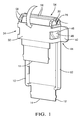
- Figs. 1 , 2A, and 2B illustrate a non-limiting example of an apparatus 10 and a flat flexible cable, hereafter the FFC 12.
- the apparatus 10 is configured to shape the FFC 12 such that a first end 14 and a second end 16 of the FFC 12 can be positioned, respectively, at a first location 18 ( Fig. 3 ) and a second location 20 ( Figs. 4 and 5 ) of a circuit board assembly, hereafter the CBA 22.
- the apparatus 10 is configured to form or bend the FFC 12 in a controlled manner so as to not cause a crease in the FFC 12.
- a crease is generally characterized as a bend with a radius that is too small and may cause an unacceptable change in the electrical impedance of the FFC 12.
- the apparatus is also configured to hold the FFC 12 in the shape formed by the apparatus 10 so the first end 14 and/or the second end 16 do not impart a spring force at the first location 18 and/or the second location 20 that may, for example, strain connections to, or force apart, a first printed circuit board, hereafter the first PCB 24 and a second circuit board, hereafter the second PCB 26, which make up the CBA 22.
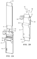
- Fig. 2A shows the apparatus 10 and the FFC 12 as separate parts before the FFC 12 is installed into the apparatus 10.
- a suitable example of the FFC 12 is a Shielded Flexible Flat Cable from Sumitomo Electric Interconnect Products of Singapore.
- the apparatus 10 includes or defines a radiused portion 30 configured to determine a bend radius of the FFC 12 after the FFC 12 is installed into the apparatus 10.
- the apparatus 10 also includes or defines a clamp portion 32 configured to urge the FFC 12 around the radiused portion when the clamp portion 32 is operated from an open position 36 ( Figs. 2A, 2B , 3 , and 4 ) to a clamped position 34 ( Figs. 1 and 5 ), whereby the FFC 12 is installed into the apparatus 10.
- the radiused portion 30 may have a radius 28 of five millimeters (5mm).
- the FFC 12 is 'installed' into the apparatus 10 after the FFC 12 is inserted into the apparatus 10 as shown in Fig. 2B and the clamp portion 32 is operated to the clamped position 34 as shown in Figs. 1 and 5 .
- the FFC 12 may be inserted into the apparatus 10 as indicated by arrow 42 in Fig. 2B to form an arrangement 38.
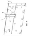
- the arrangement 38 may then be attached to the first PCB 24 as shown in Fig. 3 .
- the attachment may be by way of an adhesive, or double-sided-tape, or pins (not shown) and/or fasteners (not shown) on the underside of the apparatus 10 cooperating with holes (not shown) in the first PCB 24.
- the second PCB 26 may be placed adjacent to the first PCB 24 as shown in Fig. 4 , and the clamp portion 32 operated to the clamped position 34 as indicated by arrow 40 in Fig. 5 .
- the arrangement 38 shown in Fig. 1 the arrangement 38 shown in Fig.
- 2B may have the clamp portion 32 operated to the clamped position 34 prior to attaching the apparatus 10 with the FFC 12 already installed to the first PCB 24 with the second PCB 26 already located proximate to the first PCB 24. It is recognized that other sequences of steps may be suitable to assemble the CBA 22 shown in Fig. 5 .
- the apparatus 10 may include a latch 44 configured to hold or retain the clamp portion 32 in the clamped position 34 after the FFC 12 is installed into the apparatus 10.
- the latch 44 includes an opening 46 that cooperates with a tang 48 to hold or retain the clamp portion 32 in the clamped position 34 once operated thereto.
- the function of the latch 44 could be provided by a wide variety of other features.
- the apparatus 10 may be configured to define a tab 50 useful to urge the clamp portion 32 from the open position 36 toward a clamped position 34.
- the configuration of the tab 50 in this non-limiting example is advantageous as it limits how far the clamp portion 32 can be operated when the tab 50 contacts the first PCB, and thereby possibly preventing damaged to the FFC 12 by over-rotating the clamp portion 32.
- the non-limiting example of the apparatus 10 presented herein is configured so the clamp portion 32 is coupled to a base portion 52 of the apparatus by a flexible portion 54 configured to urge the FCC 12 against the radiused portion 30 when the FFC 12 is installed into the apparatus 10.
- the flexible portion 54 may include an alternating pattern of ribs 56 that provide strength to press the FFC 12 toward the radiused portion 30, and thin sections 58 that provide for the flexibility of the flexible portion 54.
- a suitable material for a unitary embodiment of the apparatus 10 configured with the features described herein is an injection molding grade polypropylene available from a number of commercial sources, as will be recognized by those in the art.
- the flexible portion 54 may be excluded, and the clamp portion 32 replaced by a separate part that slides over and cooperates with another separate part that includes the base portion 52 and radiused portion 30.
- This alternative may be advantageous if an apparatus with the FFC already installed similar to that shown in Fig. 1 is envisioned as a pre-assembled part prior to installing onto the first PCB 24 and/or the second PCB 26.
- an apparatus 10 configured to shape a flat flexible cable (the FFC 12) is provided.
- the apparatus 10 advantageously holds the FFC in the desire shape so that the FFC does not impart forces or strain onto the printed circuit boards of the CBA 22 or connectors mounted thereon.
- the shape imparted onto the FFC 12 is determined by a radiused portion 30 of the apparatus 10 which limits the radius formed into the FFC 12 to some minimum value so the FFC 12 is not damaged by a crease in the FFC 12.
- the apparatus 10 is also configured so an arrangement 38 of the FFC 12 and the apparatus 10 in the open position 36 can be installed onto the first PCB 24, and then the second PCB can be placed over the first PCB 24 and the arrangement 38 prior to operating the clamp portion 32 to the clamped position 34.
Landscapes
- Engineering & Computer Science (AREA)
- Microelectronics & Electronic Packaging (AREA)
- Manufacturing & Machinery (AREA)
- Installation Of Indoor Wiring (AREA)
- Coupling Device And Connection With Printed Circuit (AREA)
- Insulated Conductors (AREA)
- Insertion, Bundling And Securing Of Wires For Electric Apparatuses (AREA)
- Accessory Devices And Overall Control Thereof (AREA)
Abstract
Description
- This disclosure generally relates to an apparatus configured to shape a flat flexible cable (FFC) for installation onto a circuit board assembly, and more particularly relates to a radiused portion of the apparatus configured to determine or limit a minimum bend radius of the FFC when the FFC is installed into the apparatus.
- Conventional ribbon cables that consist of many wires arranged in parallel and encapsulated in electrical insulation material are known. However, as the operating frequencies of electronic circuits increase, these conventional ribbon cables may not provide adequate impedance control and/or shielding for some applications. In response, the electrical interconnect industry has introduced impedance controlled flexible flat conductor (FFC) that overlays the simple ribbon cable with one or more layers of conductive material to provide the desired shielding and impedance requirements. Unfortunately, these layers make the FFC stiffer than the conventional ribbon cable, so the FFC may act as a spring when the FFC is formed or shaped to include, for example, a 180 degree bend in order to interconnect two adjacent and parallel oriented printed circuit boards (PCBs). The spring effect may make handling, bending, and connecting the FFC a challenge; and may apply a spring load between parts (e.g. adjacent PCBs) interconnected by the FFC, which may lift a printed circuit board (PCB) away from locator posts that are part of a circuit board assembly (CBA). One way to overcome the spring load effect is to form a crease in the FFC. However, this often causes the impedance of the FFC to increase to greater than a desired level, greater than 100 Ohms for example.
- In accordance with one embodiment, an apparatus configured to shape a flat flexible cable (FFC) is provided. The apparatus is configured such that a first end and a second end of the FFC can be positioned, respectively, at a first location and a second location of a circuit board assembly (CBA). The apparatus includes a radiused portion configured to determine a bend radius of the FFC after the FFC is installed into the apparatus. The apparatus also includes a clamp portion configured to urge the FFC around the radiused portion when the clamp is operated to a clamped position, whereby the FFC is installed into the apparatus.
- Further features and advantages will appear more clearly on a reading of the following detailed description of the preferred embodiment, which is given by way of non-limiting example only and with reference to the accompanying drawings.
- The present invention will now be described, by way of example with reference to the accompanying drawings, in which:
-
Fig. 1 is an apparatus with a flat flexible cable (FFC) installed and operated to form a bend in the FFC with a bend radius in accordance with one embodiment; -
Fig. 2A is the apparatus ofFig. 1 prior to installing the FCC in accordance with one embodiment; -
Fig. 2B is the apparatus ofFig. 1 after to installing the FCC but before bending the FCC in accordance with one embodiment; -
Fig. 3 is a part of a circuit board assembly with the apparatus/FCC arrangement ofFig. 2B in accordance with one embodiment; -
Fig. 4 is a circuit board assembly with the apparatus/FCC arrangement ofFig. 2B in accordance with one embodiment; and -
Fig. 5 is the circuit board assembly with the apparatus/FCC arrangement ofFig. 1 in accordance with one embodiment. -
Figs. 1 ,2A, and 2B illustrate a non-limiting example of anapparatus 10 and a flat flexible cable, hereafter theFFC 12. In general, theapparatus 10 is configured to shape theFFC 12 such that afirst end 14 and asecond end 16 of the FFC 12 can be positioned, respectively, at a first location 18 (Fig. 3 ) and a second location 20 (Figs. 4 and5 ) of a circuit board assembly, hereafter the CBA 22. As will be explained in more detail below, theapparatus 10 is configured to form or bend theFFC 12 in a controlled manner so as to not cause a crease in theFFC 12. A crease is generally characterized as a bend with a radius that is too small and may cause an unacceptable change in the electrical impedance of theFFC 12. The apparatus is also configured to hold theFFC 12 in the shape formed by theapparatus 10 so thefirst end 14 and/or thesecond end 16 do not impart a spring force at thefirst location 18 and/or thesecond location 20 that may, for example, strain connections to, or force apart, a first printed circuit board, hereafter thefirst PCB 24 and a second circuit board, hereafter thesecond PCB 26, which make up the CBA 22. -
Fig. 2A shows theapparatus 10 and the FFC 12 as separate parts before the FFC 12 is installed into theapparatus 10. By way of example and not limitation, a suitable example of the FFC 12 is a Shielded Flexible Flat Cable from Sumitomo Electric Interconnect Products of Singapore. - The
apparatus 10 includes or defines aradiused portion 30 configured to determine a bend radius of theFFC 12 after theFFC 12 is installed into theapparatus 10. Theapparatus 10 also includes or defines aclamp portion 32 configured to urge theFFC 12 around the radiused portion when theclamp portion 32 is operated from an open position 36 (Figs. 2A, 2B ,3 , and4 ) to a clamped position 34 (Figs. 1 and5 ), whereby the FFC 12 is installed into theapparatus 10. By way of example and not limitation, theradiused portion 30 may have aradius 28 of five millimeters (5mm). As used herein, the FFC 12 is 'installed' into theapparatus 10 after theFFC 12 is inserted into theapparatus 10 as shown inFig. 2B and theclamp portion 32 is operated to the clampedposition 34 as shown inFigs. 1 and5 . - In one build scenario, the
FFC 12 may be inserted into theapparatus 10 as indicated byarrow 42 inFig. 2B to form anarrangement 38. Thearrangement 38 may then be attached to thefirst PCB 24 as shown inFig. 3 . The attachment may be by way of an adhesive, or double-sided-tape, or pins (not shown) and/or fasteners (not shown) on the underside of theapparatus 10 cooperating with holes (not shown) in thefirst PCB 24. Then thesecond PCB 26 may be placed adjacent to thefirst PCB 24 as shown inFig. 4 , and theclamp portion 32 operated to the clampedposition 34 as indicated byarrow 40 inFig. 5 . Alternatively, as shown inFig. 1 , thearrangement 38 shown inFig. 2B may have theclamp portion 32 operated to the clampedposition 34 prior to attaching theapparatus 10 with theFFC 12 already installed to thefirst PCB 24 with thesecond PCB 26 already located proximate to thefirst PCB 24. It is recognized that other sequences of steps may be suitable to assemble theCBA 22 shown inFig. 5 . - Referring again to
Fig. 1 , theapparatus 10 may include alatch 44 configured to hold or retain theclamp portion 32 in the clampedposition 34 after the FFC 12 is installed into theapparatus 10. In this non-limiting example, thelatch 44 includes anopening 46 that cooperates with atang 48 to hold or retain theclamp portion 32 in the clampedposition 34 once operated thereto. Those in the art will recognize that the function of thelatch 44 could be provided by a wide variety of other features. - In order to provide something to grasp when operating the
clamp portion 32, theapparatus 10 may be configured to define atab 50 useful to urge theclamp portion 32 from theopen position 36 toward a clampedposition 34. The configuration of thetab 50 in this non-limiting example is advantageous as it limits how far theclamp portion 32 can be operated when thetab 50 contacts the first PCB, and thereby possibly preventing damaged to theFFC 12 by over-rotating theclamp portion 32. - The non-limiting example of the
apparatus 10 presented herein is configured so theclamp portion 32 is coupled to abase portion 52 of the apparatus by aflexible portion 54 configured to urge the FCC 12 against theradiused portion 30 when the FFC 12 is installed into theapparatus 10. Theflexible portion 54 may include an alternating pattern ofribs 56 that provide strength to press theFFC 12 toward theradiused portion 30, andthin sections 58 that provide for the flexibility of theflexible portion 54. A suitable material for a unitary embodiment of theapparatus 10 configured with the features described herein is an injection molding grade polypropylene available from a number of commercial sources, as will be recognized by those in the art. Alternatively, theflexible portion 54 may be excluded, and theclamp portion 32 replaced by a separate part that slides over and cooperates with another separate part that includes thebase portion 52 and radiusedportion 30. This alternative may be advantageous if an apparatus with the FFC already installed similar to that shown inFig. 1 is envisioned as a pre-assembled part prior to installing onto thefirst PCB 24 and/or thesecond PCB 26. - Accordingly, an
apparatus 10 configured to shape a flat flexible cable (the FFC 12) is provided. Theapparatus 10 advantageously holds the FFC in the desire shape so that the FFC does not impart forces or strain onto the printed circuit boards of the CBA 22 or connectors mounted thereon. The shape imparted onto theFFC 12 is determined by aradiused portion 30 of theapparatus 10 which limits the radius formed into theFFC 12 to some minimum value so theFFC 12 is not damaged by a crease in theFFC 12. Theapparatus 10 is also configured so anarrangement 38 of theFFC 12 and theapparatus 10 in theopen position 36 can be installed onto thefirst PCB 24, and then the second PCB can be placed over thefirst PCB 24 and thearrangement 38 prior to operating theclamp portion 32 to the clampedposition 34. - While this invention has been described in terms of the preferred embodiments thereof, it is not intended to be so limited, but rather only to the extent set forth in the claims that follow.
Claims (4)
- An apparatus (10) configured to shape a flat flexible cable (FFC (12)) such that a first end (14) and a second end (16) of the FFC (12) can be positioned at a first location (18) and a second location (20) of a circuit board assembly (CBA (22)), said apparatus (10) comprising:a radiused portion (30) configured to determine a bend radius (28) of the FFC (12) after the FFC (12) is installed into the apparatus (10); anda clamp portion (32) configured to urge the FFC (12) around the radiused portion (30) when the clamped portion is operated to a clamped position (34), whereby the FFC (12) is installed into the apparatus (10).
- The apparatus (10) in accordance with claim 1, wherein the apparatus (10) includes a latch (44) configured to retain the clamp portion (32) in a clamped position (34) after the FFC (12) is installed into the apparatus ( 10).
- The apparatus (10) in accordance with claim 1 or 2, wherein the apparatus (10) is configured to define a tab (50) useful to urge the clamp portion (32) from an open position (36) toward a clamped position (34).
- The apparatus (10) in accordance with any one of claims 1 to 3, wherein the clamp portion (32) is coupled to a base portion (52) of the apparatus (10) by a flexible portion (54) configured to urge the FFC (12) against the radiused portion (30) after the FFC (12) is installed into the apparatus (10).
Applications Claiming Priority (1)
| Application Number | Priority Date | Filing Date | Title |
|---|---|---|---|
| US14/559,057 US20160163428A1 (en) | 2014-12-03 | 2014-12-03 | Apparatus to form a radiused bend in a flat flexible cable |
Publications (4)
| Publication Number | Publication Date |
|---|---|
| EP3030056A2 true EP3030056A2 (en) | 2016-06-08 |
| EP3030056A3 EP3030056A3 (en) | 2017-01-11 |
| EP3030056B1 EP3030056B1 (en) | 2018-11-14 |
| EP3030056B8 EP3030056B8 (en) | 2019-01-23 |
Family
ID=54705392
Family Applications (1)
| Application Number | Title | Priority Date | Filing Date |
|---|---|---|---|
| EP15195830.3A Active EP3030056B8 (en) | 2014-12-03 | 2015-11-23 | Apparatus to form a radiused bend in a flat flexible cable |
Country Status (3)
| Country | Link |
|---|---|
| US (1) | US20160163428A1 (en) |
| EP (1) | EP3030056B8 (en) |
| CN (1) | CN105680219A (en) |
Families Citing this family (1)
| Publication number | Priority date | Publication date | Assignee | Title |
|---|---|---|---|---|
| US11026324B2 (en) | 2019-02-19 | 2021-06-01 | International Business Machines Corporation | Creating a secure volume |
Family Cites Families (6)
| Publication number | Priority date | Publication date | Assignee | Title |
|---|---|---|---|---|
| JPH04311091A (en) * | 1991-04-09 | 1992-11-02 | Nec Corp | Flat cable clamp |
| US6166332A (en) * | 1998-11-20 | 2000-12-26 | International Business Machines Corporation | Method and apparatus for controlling the bend in a ribbon cable |
| US6194664B1 (en) * | 1999-06-07 | 2001-02-27 | International Business Machines Corporation | Apparatus for isolating and reinforcing bend corners of flexible cable |
| TWI228616B (en) * | 1999-11-30 | 2005-03-01 | Samsung Electronics Co Ltd | Liquid crystal display device |
| JP2002142331A (en) * | 2000-10-31 | 2002-05-17 | Yazaki Corp | Flexible circuit take-out structure |
| WO2007124113A2 (en) * | 2006-04-21 | 2007-11-01 | Neoconix, Inc. | Clamping a flat flex cable and spring contacts to a circuit board |
-
2014
- 2014-12-03 US US14/559,057 patent/US20160163428A1/en not_active Abandoned
-
2015
- 2015-11-02 CN CN201510916313.6A patent/CN105680219A/en active Pending
- 2015-11-23 EP EP15195830.3A patent/EP3030056B8/en active Active
Non-Patent Citations (1)
| Title |
|---|
| None |
Also Published As
| Publication number | Publication date |
|---|---|
| EP3030056B8 (en) | 2019-01-23 |
| EP3030056B1 (en) | 2018-11-14 |
| CN105680219A (en) | 2016-06-15 |
| EP3030056A3 (en) | 2017-01-11 |
| US20160163428A1 (en) | 2016-06-09 |
Similar Documents
| Publication | Publication Date | Title |
|---|---|---|
| US7874870B1 (en) | Coaxial cable connector with a connection terminal having a resilient tongue section | |
| CN103107429B (en) | Clamping element | |
| US9705259B2 (en) | Electrical connector part having a resistance coding | |
| EP3920337B1 (en) | Connector having latching pins that change angle for mounting to a circuit board | |
| EP2312698B1 (en) | Electrical connector | |
| CN105474466A (en) | Terminal for contacting an electric conductor | |
| CN103811885A (en) | Single Element Wire-to-Board Connectors | |
| EP2339592A2 (en) | Cable, cable connector and cable assembly | |
| KR102316920B1 (en) | Printed circuit board with side access termination pads | |
| TW200644343A (en) | Printed circuit board, connector, and electronic device | |
| CN102882032A (en) | Terminal and connector having the same | |
| EP3407428A1 (en) | Metal leaf spring structure of electrical connection terminal | |
| EP3196461A3 (en) | System, method and means for connecting and fixing an electronic control to an airtight compressor and an airtight compressor | |
| US8022300B2 (en) | Wiring harness | |
| EP3030056B1 (en) | Apparatus to form a radiused bend in a flat flexible cable | |
| CN104919903A (en) | Manufacturing and assembly procedures for electronic boards and electronic devices obtainable therefrom | |
| KR200475227Y1 (en) | Illumination apparatus using usb port | |
| US7674127B2 (en) | Electrical contact-making element | |
| US9119300B2 (en) | Motor control device | |
| US8313341B1 (en) | Guide element for a connector device | |
| CN112394303A (en) | Apparatus and method for identifying the presence of a plug on an electronic circuit board | |
| JP6180388B2 (en) | Flat cable | |
| EP3701593B1 (en) | System comprising an electrical terminal having a cage clamp for wire termination | |
| US10292272B2 (en) | Device for the orientation of contact terminals on an electrical component for fitting to a circuit board of an electric circuit | |
| US10950985B2 (en) | Shield connection element for a printed circuit board |
Legal Events
| Date | Code | Title | Description |
|---|---|---|---|
| PUAI | Public reference made under article 153(3) epc to a published international application that has entered the european phase |
Free format text: ORIGINAL CODE: 0009012 |
|
| AK | Designated contracting states |
Kind code of ref document: A2 Designated state(s): AL AT BE BG CH CY CZ DE DK EE ES FI FR GB GR HR HU IE IS IT LI LT LU LV MC MK MT NL NO PL PT RO RS SE SI SK SM TR |
|
| AX | Request for extension of the european patent |
Extension state: BA ME |
|
| PUAL | Search report despatched |
Free format text: ORIGINAL CODE: 0009013 |
|
| AK | Designated contracting states |
Kind code of ref document: A3 Designated state(s): AL AT BE BG CH CY CZ DE DK EE ES FI FR GB GR HR HU IE IS IT LI LT LU LV MC MK MT NL NO PL PT RO RS SE SI SK SM TR |
|
| AX | Request for extension of the european patent |
Extension state: BA ME |
|
| RIC1 | Information provided on ipc code assigned before grant |
Ipc: H05K 1/14 20060101ALI20161202BHEP Ipc: H05K 1/02 20060101AFI20161202BHEP |
|
| 17P | Request for examination filed |
Effective date: 20170711 |
|
| RBV | Designated contracting states (corrected) |
Designated state(s): AL AT BE BG CH CY CZ DE DK EE ES FI FR GB GR HR HU IE IS IT LI LT LU LV MC MK MT NL NO PL PT RO RS SE SI SK SM TR |
|
| GRAP | Despatch of communication of intention to grant a patent |
Free format text: ORIGINAL CODE: EPIDOSNIGR1 |
|
| INTG | Intention to grant announced |
Effective date: 20180528 |
|
| GRAS | Grant fee paid |
Free format text: ORIGINAL CODE: EPIDOSNIGR3 |
|
| GRAA | (expected) grant |
Free format text: ORIGINAL CODE: 0009210 |
|
| AK | Designated contracting states |
Kind code of ref document: B1 Designated state(s): AL AT BE BG CH CY CZ DE DK EE ES FI FR GB GR HR HU IE IS IT LI LT LU LV MC MK MT NL NO PL PT RO RS SE SI SK SM TR |
|
| REG | Reference to a national code |
Ref country code: CH Ref legal event code: EP Ref country code: AT Ref legal event code: REF Ref document number: 1066392 Country of ref document: AT Kind code of ref document: T Effective date: 20181115 |
|
| REG | Reference to a national code |
Ref country code: DE Ref legal event code: R096 Ref document number: 602015019759 Country of ref document: DE Ref country code: DE Ref legal event code: R081 Ref document number: 602015019759 Country of ref document: DE Owner name: APTIV TECHNOLOGIES LIMITED, BB Free format text: FORMER OWNER: DELPHI TECHNOLOGIES, INC., TROY, MICH., US |
|
| REG | Reference to a national code |
Ref country code: IE Ref legal event code: FG4D |
|
| RAP2 | Party data changed (patent owner data changed or rights of a patent transferred) |
Owner name: APTIV TECHNOLOGIES LIMITED |
|
| REG | Reference to a national code |
Ref country code: CH Ref legal event code: PK Free format text: BERICHTIGUNG B8 |
|
| REG | Reference to a national code |
Ref country code: GB Ref legal event code: 732E Free format text: REGISTERED BETWEEN 20190117 AND 20190123 |
|
| REG | Reference to a national code |
Ref country code: GB Ref legal event code: 732E Free format text: REGISTERED BETWEEN 20190124 AND 20190130 |
|
| REG | Reference to a national code |
Ref country code: NL Ref legal event code: MP Effective date: 20181114 |
|
| REG | Reference to a national code |
Ref country code: LT Ref legal event code: MG4D |
|
| REG | Reference to a national code |
Ref country code: AT Ref legal event code: MK05 Ref document number: 1066392 Country of ref document: AT Kind code of ref document: T Effective date: 20181114 |
|
| PG25 | Lapsed in a contracting state [announced via postgrant information from national office to epo] |
Ref country code: IS Free format text: LAPSE BECAUSE OF FAILURE TO SUBMIT A TRANSLATION OF THE DESCRIPTION OR TO PAY THE FEE WITHIN THE PRESCRIBED TIME-LIMIT Effective date: 20190314 Ref country code: ES Free format text: LAPSE BECAUSE OF FAILURE TO SUBMIT A TRANSLATION OF THE DESCRIPTION OR TO PAY THE FEE WITHIN THE PRESCRIBED TIME-LIMIT Effective date: 20181114 Ref country code: BG Free format text: LAPSE BECAUSE OF FAILURE TO SUBMIT A TRANSLATION OF THE DESCRIPTION OR TO PAY THE FEE WITHIN THE PRESCRIBED TIME-LIMIT Effective date: 20190214 Ref country code: LT Free format text: LAPSE BECAUSE OF FAILURE TO SUBMIT A TRANSLATION OF THE DESCRIPTION OR TO PAY THE FEE WITHIN THE PRESCRIBED TIME-LIMIT Effective date: 20181114 Ref country code: HR Free format text: LAPSE BECAUSE OF FAILURE TO SUBMIT A TRANSLATION OF THE DESCRIPTION OR TO PAY THE FEE WITHIN THE PRESCRIBED TIME-LIMIT Effective date: 20181114 Ref country code: AT Free format text: LAPSE BECAUSE OF FAILURE TO SUBMIT A TRANSLATION OF THE DESCRIPTION OR TO PAY THE FEE WITHIN THE PRESCRIBED TIME-LIMIT Effective date: 20181114 Ref country code: LV Free format text: LAPSE BECAUSE OF FAILURE TO SUBMIT A TRANSLATION OF THE DESCRIPTION OR TO PAY THE FEE WITHIN THE PRESCRIBED TIME-LIMIT Effective date: 20181114 Ref country code: NO Free format text: LAPSE BECAUSE OF FAILURE TO SUBMIT A TRANSLATION OF THE DESCRIPTION OR TO PAY THE FEE WITHIN THE PRESCRIBED TIME-LIMIT Effective date: 20190214 Ref country code: FI Free format text: LAPSE BECAUSE OF FAILURE TO SUBMIT A TRANSLATION OF THE DESCRIPTION OR TO PAY THE FEE WITHIN THE PRESCRIBED TIME-LIMIT Effective date: 20181114 |
|
| PG25 | Lapsed in a contracting state [announced via postgrant information from national office to epo] |
Ref country code: SE Free format text: LAPSE BECAUSE OF FAILURE TO SUBMIT A TRANSLATION OF THE DESCRIPTION OR TO PAY THE FEE WITHIN THE PRESCRIBED TIME-LIMIT Effective date: 20181114 Ref country code: AL Free format text: LAPSE BECAUSE OF FAILURE TO SUBMIT A TRANSLATION OF THE DESCRIPTION OR TO PAY THE FEE WITHIN THE PRESCRIBED TIME-LIMIT Effective date: 20181114 Ref country code: PT Free format text: LAPSE BECAUSE OF FAILURE TO SUBMIT A TRANSLATION OF THE DESCRIPTION OR TO PAY THE FEE WITHIN THE PRESCRIBED TIME-LIMIT Effective date: 20190314 Ref country code: RS Free format text: LAPSE BECAUSE OF FAILURE TO SUBMIT A TRANSLATION OF THE DESCRIPTION OR TO PAY THE FEE WITHIN THE PRESCRIBED TIME-LIMIT Effective date: 20181114 Ref country code: GR Free format text: LAPSE BECAUSE OF FAILURE TO SUBMIT A TRANSLATION OF THE DESCRIPTION OR TO PAY THE FEE WITHIN THE PRESCRIBED TIME-LIMIT Effective date: 20190215 Ref country code: NL Free format text: LAPSE BECAUSE OF FAILURE TO SUBMIT A TRANSLATION OF THE DESCRIPTION OR TO PAY THE FEE WITHIN THE PRESCRIBED TIME-LIMIT Effective date: 20181114 |
|
| REG | Reference to a national code |
Ref country code: CH Ref legal event code: PL |
|
| PG25 | Lapsed in a contracting state [announced via postgrant information from national office to epo] |
Ref country code: CZ Free format text: LAPSE BECAUSE OF FAILURE TO SUBMIT A TRANSLATION OF THE DESCRIPTION OR TO PAY THE FEE WITHIN THE PRESCRIBED TIME-LIMIT Effective date: 20181114 Ref country code: LU Free format text: LAPSE BECAUSE OF NON-PAYMENT OF DUE FEES Effective date: 20181123 Ref country code: IT Free format text: LAPSE BECAUSE OF FAILURE TO SUBMIT A TRANSLATION OF THE DESCRIPTION OR TO PAY THE FEE WITHIN THE PRESCRIBED TIME-LIMIT Effective date: 20181114 Ref country code: DK Free format text: LAPSE BECAUSE OF FAILURE TO SUBMIT A TRANSLATION OF THE DESCRIPTION OR TO PAY THE FEE WITHIN THE PRESCRIBED TIME-LIMIT Effective date: 20181114 Ref country code: PL Free format text: LAPSE BECAUSE OF FAILURE TO SUBMIT A TRANSLATION OF THE DESCRIPTION OR TO PAY THE FEE WITHIN THE PRESCRIBED TIME-LIMIT Effective date: 20181114 |
|
| REG | Reference to a national code |
Ref country code: DE Ref legal event code: R097 Ref document number: 602015019759 Country of ref document: DE |
|
| REG | Reference to a national code |
Ref country code: BE Ref legal event code: MM Effective date: 20181130 |
|
| REG | Reference to a national code |
Ref country code: IE Ref legal event code: MM4A |
|
| PG25 | Lapsed in a contracting state [announced via postgrant information from national office to epo] |
Ref country code: SM Free format text: LAPSE BECAUSE OF FAILURE TO SUBMIT A TRANSLATION OF THE DESCRIPTION OR TO PAY THE FEE WITHIN THE PRESCRIBED TIME-LIMIT Effective date: 20181114 Ref country code: SK Free format text: LAPSE BECAUSE OF FAILURE TO SUBMIT A TRANSLATION OF THE DESCRIPTION OR TO PAY THE FEE WITHIN THE PRESCRIBED TIME-LIMIT Effective date: 20181114 Ref country code: RO Free format text: LAPSE BECAUSE OF FAILURE TO SUBMIT A TRANSLATION OF THE DESCRIPTION OR TO PAY THE FEE WITHIN THE PRESCRIBED TIME-LIMIT Effective date: 20181114 Ref country code: LI Free format text: LAPSE BECAUSE OF NON-PAYMENT OF DUE FEES Effective date: 20181130 Ref country code: CH Free format text: LAPSE BECAUSE OF NON-PAYMENT OF DUE FEES Effective date: 20181130 Ref country code: MC Free format text: LAPSE BECAUSE OF FAILURE TO SUBMIT A TRANSLATION OF THE DESCRIPTION OR TO PAY THE FEE WITHIN THE PRESCRIBED TIME-LIMIT Effective date: 20181114 Ref country code: EE Free format text: LAPSE BECAUSE OF FAILURE TO SUBMIT A TRANSLATION OF THE DESCRIPTION OR TO PAY THE FEE WITHIN THE PRESCRIBED TIME-LIMIT Effective date: 20181114 |
|
| PLBE | No opposition filed within time limit |
Free format text: ORIGINAL CODE: 0009261 |
|
| STAA | Information on the status of an ep patent application or granted ep patent |
Free format text: STATUS: NO OPPOSITION FILED WITHIN TIME LIMIT |
|
| 26N | No opposition filed |
Effective date: 20190815 |
|
| PG25 | Lapsed in a contracting state [announced via postgrant information from national office to epo] |
Ref country code: IE Free format text: LAPSE BECAUSE OF NON-PAYMENT OF DUE FEES Effective date: 20181123 Ref country code: SI Free format text: LAPSE BECAUSE OF FAILURE TO SUBMIT A TRANSLATION OF THE DESCRIPTION OR TO PAY THE FEE WITHIN THE PRESCRIBED TIME-LIMIT Effective date: 20181114 |
|
| PG25 | Lapsed in a contracting state [announced via postgrant information from national office to epo] |
Ref country code: BE Free format text: LAPSE BECAUSE OF NON-PAYMENT OF DUE FEES Effective date: 20181130 |
|
| PG25 | Lapsed in a contracting state [announced via postgrant information from national office to epo] |
Ref country code: MT Free format text: LAPSE BECAUSE OF NON-PAYMENT OF DUE FEES Effective date: 20181123 |
|
| PG25 | Lapsed in a contracting state [announced via postgrant information from national office to epo] |
Ref country code: TR Free format text: LAPSE BECAUSE OF FAILURE TO SUBMIT A TRANSLATION OF THE DESCRIPTION OR TO PAY THE FEE WITHIN THE PRESCRIBED TIME-LIMIT Effective date: 20181114 |
|
| PG25 | Lapsed in a contracting state [announced via postgrant information from national office to epo] |
Ref country code: MK Free format text: LAPSE BECAUSE OF NON-PAYMENT OF DUE FEES Effective date: 20181114 Ref country code: CY Free format text: LAPSE BECAUSE OF FAILURE TO SUBMIT A TRANSLATION OF THE DESCRIPTION OR TO PAY THE FEE WITHIN THE PRESCRIBED TIME-LIMIT Effective date: 20181114 Ref country code: HU Free format text: LAPSE BECAUSE OF FAILURE TO SUBMIT A TRANSLATION OF THE DESCRIPTION OR TO PAY THE FEE WITHIN THE PRESCRIBED TIME-LIMIT; INVALID AB INITIO Effective date: 20151123 |
|
| P01 | Opt-out of the competence of the unified patent court (upc) registered |
Effective date: 20230425 |
|
| REG | Reference to a national code |
Ref country code: DE Ref legal event code: R081 Ref document number: 602015019759 Country of ref document: DE Owner name: APTIV TECHNOLOGIES AG, CH Free format text: FORMER OWNER: APTIV TECHNOLOGIES LIMITED, ST. MICHAEL, BB |
|
| PGFP | Annual fee paid to national office [announced via postgrant information from national office to epo] |
Ref country code: DE Payment date: 20251010 Year of fee payment: 11 |
|
| PGFP | Annual fee paid to national office [announced via postgrant information from national office to epo] |
Ref country code: GB Payment date: 20251107 Year of fee payment: 11 |
|
| PGFP | Annual fee paid to national office [announced via postgrant information from national office to epo] |
Ref country code: FR Payment date: 20251112 Year of fee payment: 11 |